EP0964437A2 - Procédé pour fabriquer des dispositifs à circuits intégrés semi-conducteurs et circuits intégrés semi-conducteurs - Google Patents
Procédé pour fabriquer des dispositifs à circuits intégrés semi-conducteurs et circuits intégrés semi-conducteurs Download PDFInfo
- Publication number
- EP0964437A2 EP0964437A2 EP99303683A EP99303683A EP0964437A2 EP 0964437 A2 EP0964437 A2 EP 0964437A2 EP 99303683 A EP99303683 A EP 99303683A EP 99303683 A EP99303683 A EP 99303683A EP 0964437 A2 EP0964437 A2 EP 0964437A2
- Authority
- EP
- European Patent Office
- Prior art keywords
- film
- polycrystalline silicon
- refractory metal
- integrated circuit
- gate electrode
- Prior art date
- Legal status (The legal status is an assumption and is not a legal conclusion. Google has not performed a legal analysis and makes no representation as to the accuracy of the status listed.)
- Withdrawn
Links
Images










Classifications
-
- H—ELECTRICITY
- H10—SEMICONDUCTOR DEVICES; ELECTRIC SOLID-STATE DEVICES NOT OTHERWISE PROVIDED FOR
- H10D—INORGANIC ELECTRIC SEMICONDUCTOR DEVICES
- H10D64/00—Electrodes of devices having potential barriers
- H10D64/01—Manufacture or treatment
- H10D64/013—Manufacture or treatment of electrodes having a conductor capacitively coupled to a semiconductor by an insulator
- H10D64/01302—Manufacture or treatment of electrodes having a conductor capacitively coupled to a semiconductor by an insulator the insulator being formed after the semiconductor body, the semiconductor being silicon
- H10D64/01354—Manufacture or treatment of electrodes having a conductor capacitively coupled to a semiconductor by an insulator the insulator being formed after the semiconductor body, the semiconductor being silicon passivation or protection of the electrode, e.g. using re-oxidation
-
- H—ELECTRICITY
- H10—SEMICONDUCTOR DEVICES; ELECTRIC SOLID-STATE DEVICES NOT OTHERWISE PROVIDED FOR
- H10D—INORGANIC ELECTRIC SEMICONDUCTOR DEVICES
- H10D30/00—Field-effect transistors [FET]
- H10D30/60—Insulated-gate field-effect transistors [IGFET]
-
- H—ELECTRICITY
- H10—SEMICONDUCTOR DEVICES; ELECTRIC SOLID-STATE DEVICES NOT OTHERWISE PROVIDED FOR
- H10D—INORGANIC ELECTRIC SEMICONDUCTOR DEVICES
- H10D64/00—Electrodes of devices having potential barriers
- H10D64/01—Manufacture or treatment
- H10D64/013—Manufacture or treatment of electrodes having a conductor capacitively coupled to a semiconductor by an insulator
- H10D64/01302—Manufacture or treatment of electrodes having a conductor capacitively coupled to a semiconductor by an insulator the insulator being formed after the semiconductor body, the semiconductor being silicon
- H10D64/01304—Manufacture or treatment of electrodes having a conductor capacitively coupled to a semiconductor by an insulator the insulator being formed after the semiconductor body, the semiconductor being silicon characterised by the conductor
- H10D64/01306—Manufacture or treatment of electrodes having a conductor capacitively coupled to a semiconductor by an insulator the insulator being formed after the semiconductor body, the semiconductor being silicon characterised by the conductor the conductor comprising a layer of silicon contacting the insulator, e.g. polysilicon
- H10D64/01308—Manufacture or treatment of electrodes having a conductor capacitively coupled to a semiconductor by an insulator the insulator being formed after the semiconductor body, the semiconductor being silicon characterised by the conductor the conductor comprising a layer of silicon contacting the insulator, e.g. polysilicon the conductor further comprising a non-elemental silicon additional conductive layer, e.g. a metal silicide layer formed by the reaction of silicon with an implanted metal
-
- H—ELECTRICITY
- H10—SEMICONDUCTOR DEVICES; ELECTRIC SOLID-STATE DEVICES NOT OTHERWISE PROVIDED FOR
- H10D—INORGANIC ELECTRIC SEMICONDUCTOR DEVICES
- H10D64/00—Electrodes of devices having potential barriers
- H10D64/60—Electrodes characterised by their materials
- H10D64/66—Electrodes having a conductor capacitively coupled to a semiconductor by an insulator, e.g. MIS electrodes
- H10D64/661—Electrodes having a conductor capacitively coupled to a semiconductor by an insulator, e.g. MIS electrodes the conductor comprising a layer of silicon contacting the insulator, e.g. polysilicon having vertical doping variation
- H10D64/662—Electrodes having a conductor capacitively coupled to a semiconductor by an insulator, e.g. MIS electrodes the conductor comprising a layer of silicon contacting the insulator, e.g. polysilicon having vertical doping variation the conductor further comprising additional layers, e.g. multiple silicon layers having different crystal structures
- H10D64/664—Electrodes having a conductor capacitively coupled to a semiconductor by an insulator, e.g. MIS electrodes the conductor comprising a layer of silicon contacting the insulator, e.g. polysilicon having vertical doping variation the conductor further comprising additional layers, e.g. multiple silicon layers having different crystal structures the additional layers comprising a barrier layer between the layer of silicon and an upper metal or metal silicide layer
-
- H—ELECTRICITY
- H10—SEMICONDUCTOR DEVICES; ELECTRIC SOLID-STATE DEVICES NOT OTHERWISE PROVIDED FOR
- H10D—INORGANIC ELECTRIC SEMICONDUCTOR DEVICES
- H10D64/00—Electrodes of devices having potential barriers
- H10D64/60—Electrodes characterised by their materials
- H10D64/66—Electrodes having a conductor capacitively coupled to a semiconductor by an insulator, e.g. MIS electrodes
- H10D64/671—Electrodes having a conductor capacitively coupled to a semiconductor by an insulator, e.g. MIS electrodes the conductor having lateral variation in doping or structure
-
- H—ELECTRICITY
- H10—SEMICONDUCTOR DEVICES; ELECTRIC SOLID-STATE DEVICES NOT OTHERWISE PROVIDED FOR
- H10D—INORGANIC ELECTRIC SEMICONDUCTOR DEVICES
- H10D84/00—Integrated devices formed in or on semiconductor substrates that comprise only semiconducting layers, e.g. on Si wafers or on GaAs-on-Si wafers
- H10D84/01—Manufacture or treatment
- H10D84/0123—Integrating together multiple components covered by H10D12/00 or H10D30/00, e.g. integrating multiple IGBTs
- H10D84/0126—Integrating together multiple components covered by H10D12/00 or H10D30/00, e.g. integrating multiple IGBTs the components including insulated gates, e.g. IGFETs
- H10D84/0165—Integrating together multiple components covered by H10D12/00 or H10D30/00, e.g. integrating multiple IGBTs the components including insulated gates, e.g. IGFETs the components including complementary IGFETs, e.g. CMOS devices
-
- H—ELECTRICITY
- H10—SEMICONDUCTOR DEVICES; ELECTRIC SOLID-STATE DEVICES NOT OTHERWISE PROVIDED FOR
- H10D—INORGANIC ELECTRIC SEMICONDUCTOR DEVICES
- H10D84/00—Integrated devices formed in or on semiconductor substrates that comprise only semiconducting layers, e.g. on Si wafers or on GaAs-on-Si wafers
- H10D84/01—Manufacture or treatment
- H10D84/0123—Integrating together multiple components covered by H10D12/00 or H10D30/00, e.g. integrating multiple IGBTs
- H10D84/0126—Integrating together multiple components covered by H10D12/00 or H10D30/00, e.g. integrating multiple IGBTs the components including insulated gates, e.g. IGFETs
- H10D84/0165—Integrating together multiple components covered by H10D12/00 or H10D30/00, e.g. integrating multiple IGBTs the components including insulated gates, e.g. IGFETs the components including complementary IGFETs, e.g. CMOS devices
- H10D84/0172—Manufacturing their gate conductors
- H10D84/0177—Manufacturing their gate conductors the gate conductors having different materials or different implants
-
- H—ELECTRICITY
- H10—SEMICONDUCTOR DEVICES; ELECTRIC SOLID-STATE DEVICES NOT OTHERWISE PROVIDED FOR
- H10D—INORGANIC ELECTRIC SEMICONDUCTOR DEVICES
- H10D84/00—Integrated devices formed in or on semiconductor substrates that comprise only semiconducting layers, e.g. on Si wafers or on GaAs-on-Si wafers
- H10D84/01—Manufacture or treatment
- H10D84/0123—Integrating together multiple components covered by H10D12/00 or H10D30/00, e.g. integrating multiple IGBTs
- H10D84/0126—Integrating together multiple components covered by H10D12/00 or H10D30/00, e.g. integrating multiple IGBTs the components including insulated gates, e.g. IGFETs
- H10D84/0165—Integrating together multiple components covered by H10D12/00 or H10D30/00, e.g. integrating multiple IGBTs the components including insulated gates, e.g. IGFETs the components including complementary IGFETs, e.g. CMOS devices
- H10D84/0181—Manufacturing their gate insulating layers
-
- H—ELECTRICITY
- H10—SEMICONDUCTOR DEVICES; ELECTRIC SOLID-STATE DEVICES NOT OTHERWISE PROVIDED FOR
- H10D—INORGANIC ELECTRIC SEMICONDUCTOR DEVICES
- H10D84/00—Integrated devices formed in or on semiconductor substrates that comprise only semiconducting layers, e.g. on Si wafers or on GaAs-on-Si wafers
- H10D84/01—Manufacture or treatment
- H10D84/02—Manufacture or treatment characterised by using material-based technologies
- H10D84/03—Manufacture or treatment characterised by using material-based technologies using Group IV technology, e.g. silicon technology or silicon-carbide [SiC] technology
- H10D84/038—Manufacture or treatment characterised by using material-based technologies using Group IV technology, e.g. silicon technology or silicon-carbide [SiC] technology using silicon technology, e.g. SiGe
-
- H—ELECTRICITY
- H10—SEMICONDUCTOR DEVICES; ELECTRIC SOLID-STATE DEVICES NOT OTHERWISE PROVIDED FOR
- H10P—GENERIC PROCESSES OR APPARATUS FOR THE MANUFACTURE OR TREATMENT OF DEVICES COVERED BY CLASS H10
- H10P10/00—Bonding of wafers, substrates or parts of devices
-
- H—ELECTRICITY
- H10—SEMICONDUCTOR DEVICES; ELECTRIC SOLID-STATE DEVICES NOT OTHERWISE PROVIDED FOR
- H10P—GENERIC PROCESSES OR APPARATUS FOR THE MANUFACTURE OR TREATMENT OF DEVICES COVERED BY CLASS H10
- H10P14/00—Formation of materials, e.g. in the shape of layers or pillars
- H10P14/60—Formation of materials, e.g. in the shape of layers or pillars of insulating materials
- H10P14/63—Formation of materials, e.g. in the shape of layers or pillars of insulating materials characterised by the formation processes
- H10P14/6302—Non-deposition formation processes
- H10P14/6304—Formation by oxidation, e.g. oxidation of the substrate
- H10P14/6306—Formation by oxidation, e.g. oxidation of the substrate of the semiconductor materials
- H10P14/6308—Formation by oxidation, e.g. oxidation of the substrate of the semiconductor materials of Group IV semiconductors
-
- H—ELECTRICITY
- H10—SEMICONDUCTOR DEVICES; ELECTRIC SOLID-STATE DEVICES NOT OTHERWISE PROVIDED FOR
- H10P—GENERIC PROCESSES OR APPARATUS FOR THE MANUFACTURE OR TREATMENT OF DEVICES COVERED BY CLASS H10
- H10P72/00—Handling or holding of wafers, substrates or devices during manufacture or treatment thereof
- H10P72/04—Apparatus for manufacture or treatment
- H10P72/0431—Apparatus for thermal treatment
-
- H—ELECTRICITY
- H10—SEMICONDUCTOR DEVICES; ELECTRIC SOLID-STATE DEVICES NOT OTHERWISE PROVIDED FOR
- H10P—GENERIC PROCESSES OR APPARATUS FOR THE MANUFACTURE OR TREATMENT OF DEVICES COVERED BY CLASS H10
- H10P72/00—Handling or holding of wafers, substrates or devices during manufacture or treatment thereof
- H10P72/04—Apparatus for manufacture or treatment
- H10P72/0431—Apparatus for thermal treatment
- H10P72/0436—Apparatus for thermal treatment mainly by radiation
-
- H—ELECTRICITY
- H10—SEMICONDUCTOR DEVICES; ELECTRIC SOLID-STATE DEVICES NOT OTHERWISE PROVIDED FOR
- H10D—INORGANIC ELECTRIC SEMICONDUCTOR DEVICES
- H10D64/00—Electrodes of devices having potential barriers
- H10D64/01—Manufacture or treatment
- H10D64/013—Manufacture or treatment of electrodes having a conductor capacitively coupled to a semiconductor by an insulator
- H10D64/01302—Manufacture or treatment of electrodes having a conductor capacitively coupled to a semiconductor by an insulator the insulator being formed after the semiconductor body, the semiconductor being silicon
- H10D64/01304—Manufacture or treatment of electrodes having a conductor capacitively coupled to a semiconductor by an insulator the insulator being formed after the semiconductor body, the semiconductor being silicon characterised by the conductor
- H10D64/01306—Manufacture or treatment of electrodes having a conductor capacitively coupled to a semiconductor by an insulator the insulator being formed after the semiconductor body, the semiconductor being silicon characterised by the conductor the conductor comprising a layer of silicon contacting the insulator, e.g. polysilicon
- H10D64/01308—Manufacture or treatment of electrodes having a conductor capacitively coupled to a semiconductor by an insulator the insulator being formed after the semiconductor body, the semiconductor being silicon characterised by the conductor the conductor comprising a layer of silicon contacting the insulator, e.g. polysilicon the conductor further comprising a non-elemental silicon additional conductive layer, e.g. a metal silicide layer formed by the reaction of silicon with an implanted metal
- H10D64/01312—Manufacture or treatment of electrodes having a conductor capacitively coupled to a semiconductor by an insulator the insulator being formed after the semiconductor body, the semiconductor being silicon characterised by the conductor the conductor comprising a layer of silicon contacting the insulator, e.g. polysilicon the conductor further comprising a non-elemental silicon additional conductive layer, e.g. a metal silicide layer formed by the reaction of silicon with an implanted metal the additional layer comprising a metal or metal silicide formed by deposition, i.e. without a silicidation reaction, e.g. sputter deposition
-
- H—ELECTRICITY
- H10—SEMICONDUCTOR DEVICES; ELECTRIC SOLID-STATE DEVICES NOT OTHERWISE PROVIDED FOR
- H10D—INORGANIC ELECTRIC SEMICONDUCTOR DEVICES
- H10D86/00—Integrated devices formed in or on insulating or conducting substrates, e.g. formed in silicon-on-insulator [SOI] substrates or on stainless steel or glass substrates
- H10D86/40—Integrated devices formed in or on insulating or conducting substrates, e.g. formed in silicon-on-insulator [SOI] substrates or on stainless steel or glass substrates characterised by multiple TFTs
-
- H—ELECTRICITY
- H10—SEMICONDUCTOR DEVICES; ELECTRIC SOLID-STATE DEVICES NOT OTHERWISE PROVIDED FOR
- H10D—INORGANIC ELECTRIC SEMICONDUCTOR DEVICES
- H10D86/00—Integrated devices formed in or on insulating or conducting substrates, e.g. formed in silicon-on-insulator [SOI] substrates or on stainless steel or glass substrates
- H10D86/40—Integrated devices formed in or on insulating or conducting substrates, e.g. formed in silicon-on-insulator [SOI] substrates or on stainless steel or glass substrates characterised by multiple TFTs
- H10D86/60—Integrated devices formed in or on insulating or conducting substrates, e.g. formed in silicon-on-insulator [SOI] substrates or on stainless steel or glass substrates characterised by multiple TFTs wherein the TFTs are in active matrices
Definitions
- Japanese Patent Laid-Open No. 132136/1984 discloses a technique in that after forming a gate electrode of a polymetal structure containing a W film or an Mo film on an Si (silicon) substrate, light oxidation is conducted in a mixed atmosphere of steam and hydrogen to selectively oxidize only Si without oxidizing the W (Mo) film.
- Nakamura In Series of Theses of 45th Symposium of Semiconductor Integrated Circuit Techniques, held on December 1 and 2 of 1992, pp. 128 to 133, (hereinafter referred to as Nakamura) there is disclosed a technique for forming an oxide film in a strong reducing atmosphere containing steam synthesized by a stainless catalyst.
- the gate electrode material is patterned by dry etching using a photoresist as a mask. Thereafter, the photoresist is removed by ashing, and the dry etching residue and the ashing residue remaining on the surface of the substrate are removed by using an etching solution such as hydrofluoric acid.
- the light oxidation in a steam/hydrogen mixed gas having the prescribed partial pressure ratio is effective means for improving resisting voltage of the gate oxide film and preventing oxidation of the metal film.
- the steam/hydrogen mixed gas is formed by supplying a hydrogen gas to pure water set aside in a container, there is a possibility that foreign matters contained in the pure water are transferred to an oxidation furnace along with the steam/hydrogen mixed gas to contaminate a semiconductor wafer.
- the steam/hydrogen partial pressure ratio is controlled by changing the temperature of the pure water, there are problems in that (1) the partial pressure is liable to fluctuate, and it is difficult to realize the optimum partial pressure ratio with high precision, and (2) the controllable range of the steam concentration is as narrow as from several percents to several tens percents, and it is difficult to realize a steam concentration in a ppm order.
- the circuit of which is constituted by the fine MOSFET having a gate length of 0.18 ⁇ m or less
- the employment of the so-called dual gate structure is advantageous, in which in order to suppress as possible the fluctuation of the threshold voltage (V th ) due to operation at a low voltage, the conductivity type of the polycrystalline silicon film constituting the gate electrode of the n-channel MISFET is set at n-type, and the conductivity type of the polycrystalline silicon film constituting the gate electrode of the p-channel MISFET is set at p-type.
- the gate electrode of the n-channel MISFET has a structure in that a refractory metal film is laminated on an n-type polycrystalline silicon film doped with an n-type impurity, such as phosphorous (P), and the gate electrode of the p-channel MISFET has a structure in that a refractory metal film is laminated on an p-type polycrystalline silicon film doped with a p-type impurity, such as boron (B).
- the process for producing a semiconductor integrated circuit device comprises a step, in which a conductive film comprising a gate oxide film formed on a major surface of a semiconductor substrate laminated with a polycrystalline silicon film containing boron and a refractory metal film directly or through a barrier layer is formed, and a gate electrode of an MOSFET is formed by patterning the conductive film; and a heat treatment step, in which a mixed gas containing a hydrogen gas and steam synthesized from an oxygen gas and the hydrogen gas with a catalyst is supplied to the major surface or a vicinity thereof of the semiconductor substrate heated to a prescribed temperature, and a profile of the gate insulating film under an edge part of the gate electrode etched on patterning in the preceding step is improved by selectively oxidizing the major surface of the semiconductor substrate, in which the heat treatment is conducted under a low thermal load condition in that the refractory metal film is substantially not oxidized, and boron contained in the polycrystalline silicon film constituting a part of the gate electrode is not diffused to
- Fig. 4 is a partial cross sectional view of a semiconductor substrate showing a process for producing a CMOS LSI as an embodiment of the invention.
- Fig. 7 is a partial cross sectional view of a semiconductor substrate showing a process for producing a CMOS LSI as an embodiment of the invention.
- Fig. 9A is a schematic plan view showing a single wafer processing oxidation furnace used for the light oxidation process
- Fig. 9B is a cross sectional view taken on line B-B' in Fig. 9A.
- Fig. 10A is a schematic plan view showing a single wafer processing oxidation furnace used for the light oxidation process
- Fig. 10B is a cross sectional view taken on line B-B' in Fig. 10A.
- Fig. 12 is a diagram showing a conduit system of the device for generating a steam/hydrogen mixed gas shown in Fig. 11.
- Fig. 13 is a graph showing the dependency of the equilibrium vapor pressure ratio of the redox reaction using the steam/hydrogen mixed gas on the temperature.
- Fig. 15 is a graph showing the relationship between the oxidation temperature and the oxidation time.
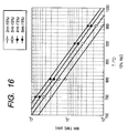
- Fig. 16 is a graph showing the relationship between the oxidation temperature and the oxidation time.
- Fig. 17 is a graph showing the relationship between the temperature on subjecting the gate electrode to the heat treatment and V FB .
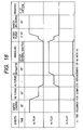
- Figs 19A and 19B are partial enlarged cross sectional views showing the state of the gate oxide film after the light oxidation process.
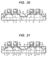
- Fig. 20 is a partial cross sectional view of a semiconductor substrate showing a process for producing a CMOS LSI as an embodiment of the invention.
- Fig. 22 is a partial cross sectional view of a semiconductor substrate showing a process for producing a CMOS LSI as an embodiment of the invention.
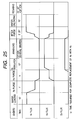
- Fig. 25 is a diagram showing the sequence of the light oxidation process using the batch processing vertical oxidation furnace.
- the semiconductor integrated circuit device referred in the invention includes not only those produced on a silicon wafer but also those produced on the other substrates, such as a TFT liquid crystal, except the case where it is clearly indicated that those are not included.
- the semiconductor wafer referred in the invention includes not only a single crystal semiconductor, such as a silicon single crystal wafer, or those obtained by forming conductive or semiconductor films directly on or via an insulating film to be a multi-layer structure, but also those obtained by forming a semiconductor part, a conductive film part and an insulating film part on a wafer of an insulating material.
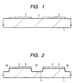
- a semiconductor substrate 1 comprising single crystal silicon having a specific resistance of about 10 ⁇ cm is subjected to a heat treatment at about 850°C to form a thin silicon oxide film 2 (pad oxide film) having a film thickness of about 10 nm on the major surface thereof, and a silicon nitride film 3 having a film thickness of about 120 nm is accumulated on the silicon oxide film 2 by a CVD (chemical vapor deposition) method, followed by removing the silicon nitride film 3 and the silicon oxide film 2 in an element isolation region by etching using a photoresist film as a mask.
- the silicon oxide film 2 is formed to relax the stress applied to the substrate on densifying a silicon oxide film embedded inside the element isolation groove in the later step. Since the silicon nitride film 3 has characteristics that it is difficult to be oxidized, it is utilized as a mask for preventing oxidation of the substrate surface thereunder (active region).
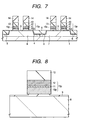
- a silicon oxide film 6 having a film thickness of about 380 nm is accumulated on the semiconductor substrate 1, and in order to improve the film quality of the silicon oxide film 6, the semiconductor substrate 1 is subjected to a heat treatment to densify the silicon oxide film 6. Then, the silicon oxide film 6 is polished by a chemical mechanical polishing (CMP) method by using the silicon nitride film 3 as a stopper to leave it inside the groove 4a, so as to form an element isolation having a flattened surface 4.
- CMP chemical mechanical polishing
- ion implantation of B (boron) for adjusting the threshold voltage (V th ) of the n-channel MISFET is conducted into the p-type well 7
- ion implantation of P (phosphorous) for adjusting the threshold voltage (V th ) of the p-channel MISFET is conducted into the n-type well 8.
- the silicon oxide film 2 on each of the p-type well 7 and the n-type well 8 is removed by using an HF (hydrofluoric acid) series cleaning solution, and the semiconductor substrate 1 is subjected to wet oxidation to form a clean gate oxide film 9 having a film thickness about 3.5 nm on the surface of each of the p-type well 7 and the n-type well 8.
- HF hydrofluoric acid
- an oxinitrification treatment to segregate nitrogen at the interface between the gate oxide film 9 and the semiconductor substrate 1 may be conducted by subjecting the semiconductor substrate 1 to a heat treatment in an NO (nitrogen oxide) or N 2 O (nitrous oxide) atmosphere.
- NO nitrogen oxide
- N 2 O nitrogen oxide
- the gate oxide film 9 is thinned to about 3.5 nm, the stress formed at the interface therebetween due to the difference in heat expansion coefficient from the semiconductor substrate 1 becomes tangible to induce generation of a hot carrier. Nitrogen segregated at the interface to the semiconductor substrate 1 relaxes the stress, and thus the oxinitrification treatment improves the reliability of the extremely thin gate oxide film 9.
- a WN film 11 having a film thickness of about 5 nm and a W film 12 having a film thickness of about 50 nm are accumulated on the n-type polycrystalline silicon film 10n and the p-type polycrystalline silicon film 10p by a sputtering method, and after a silicon nitride film 13 having a film thickness of about 200 nm is formed on the W film 12, these films are subjected to dry etching by using a photoresist film 14 formed on the silicon nitride film 13 as a mask.
- a gate electrode 15n of an n-channel MISFET comprising the n-type polycrystalline silicon film 10n, the WN film 11 and the W film 12 is formed on the gate oxide film 9 of the p-type well 7, and a gate electrode 15p of a p-channel MISFET comprising the p-type polycrystalline silicon film 10p, the WN film 11 and the W film 12 is formed on the gate oxide film 9 of the n-type well 8.
- the gate length of each of the gate electrode 15n and the gate electrode 15p is, for example, 0.18 ⁇ m.
- the sheet resistance thereof can be decreased to about 2 ⁇ per square, and thus high speed operation can be realized by controlling the gate delay of the CMOS circuit.
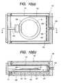
- Fig. 9A is a schematic plan view showing an example of a specific constitution of a single wafer processing oxidation furnace used for the light oxidation process
- Fig. 9B is a cross sectional view taken on line B-B' in Fig. 9A.
- the single wafer processing oxidation furnace 100 comprises a chamber 101 constituted by a multiple wall quartz tube, which has heaters 102a and 102b for heating a semiconductor wafer 1A at an upper part and a lower part thereof, respectively.
- a heat flattening ring 103 having a disk shape that uniformly disperse heat supplied from the heaters 102a and 102b to the hole surface of the semiconductor wafer 1A is installed in the chamber 101, and a susceptor 104 horizontally holding the semiconductor wafer 1A is provided at an upper part thereof.
- the heat flattening ring 103 is constituted by a heat resistant material such as quartz and SiC (silicon carbide) and supported by a supporting arm 105 extending from a wall of the chamber 101.
- thermoelectric couple 106 for measuring the temperature of the semiconductor wafer 1A supported by the susceptor 104 is provided in the vicinity of the heat flattening ring 103.
- the heating of the semiconductor wafer 1A may be conducted, for example, by an RTA (rapid thermal annealing) method using a halogen lamp 107 as shown in Fig. 10, as well as the heating method using the heaters 102a and 102b.
- RTA rapid thermal annealing
- One end of a gas introducing conduit 108 for introducing a steam/hydrogen mixed gas and a purge gas into the chamber 101 is connected to a part of the wall of the chamber 101.
- a gas generating device of a catalyst type described later is connected to the other end of the gas introducing conduit 108.
- a partition 110 having numerous through holes 109 is provided in the vicinity of the gas introducing conduit 108, and the gas introduced into the chamber 101 is uniformly spread throughout the chamber 101 passing through the through holes 109 of the partition 110.
- One end of an exhausting conduit 111 for evacuating the gas introduced into the chamber 101 is connected to the other part of the wall of the chamber 101.
- Fig. 11 is a schematic diagram showing a device for generating a steam/hydrogen mixed gas of a catalyst type connected to the chamber 101 of the single wafer processing oxidation furnace 100.
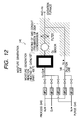
- Fig. 12 is a diagram showing a conduit system of the gas generating device.
- the gas generating device 140 comprises a reactor 141 constituted by a heat resistant and corrosion resistant alloy (for example, an Ni alloy known as "Hastelloy", a trade name), and a coil 142 comprising a catalyst metal, such as Pt (platinum), Ni (nickel) or Pd (palladium), and a heater 143 heating the coil 142 are installed inside the reactor.
- a heat resistant and corrosion resistant alloy for example, an Ni alloy known as "Hastelloy", a trade name
- a coil 142 comprising a catalyst metal, such as Pt (platinum), Ni (nickel) or Pd (palladium)
- a heater 143 heating the coil 142 are installed inside the reactor.
- a process gas comprising hydrogen and oxygen, and a purge gas comprising an inert gas, such as nitrogen or Ar (argon) are introduced into the reactor 141 from gas storage tanks 144a, 144b and 144c through a conduit 145.
- Mass flow controllers 146a, 146b and 146c for controlling the amounts of the gases and switching valves 147a, 147b and 147c are provided between the gas storage tanks 144a, 144b and 144c and the conduit 145, to precisely control the amounts and compositional ratio of the gases introduced into the reactor 141.
- the process gas (hydrogen and oxygen) introduced into the reactor 141 is excited by contacting with the coil 142 heated to a temperature of about from 350 to 450°C, so that a hydrogen radical is formed from a hydrogen molecule (H 2 ⁇ 2H*), and an oxygen radical is formed from an oxygen molecule (O 2 ⁇ 20*).
- the two kinds of radicals are extremely chemically active, and thus rapidly react to form water (2H* + O* ⁇ H 2 O).
- the mixed gas is mixed with hydrogen supplied from a dilution line 148 shown in Fig.
- the mixed gas may be introduced into the chamber 101 after diluting with an inert gas, such as nitrogen and argon, to a suitable concentration.
- the pressure of the mixed gas may be arbitrarily set within the range of from several tens Torr to several atm.
- the gas generating device 140 of a catalyst type can precisely control the amounts of hydrogen and oxygen participating in the formation of water and their ratio, the steam concentration in the steam/hydrogen mixed gas introduced into the chamber 101 can be precisely controlled within a wide range of from an extremely low concentration of a ppm order to a high concentration of several tens percent. Because water is instantaneously formed when the process gas is introduced into the reactor 141, a steam/hydrogen mixed gas having a desired steam concentration can be obtained in a real-time manner. By using such a manner, because inclusion of foreign matters is suppressed as the minimum, a clean steam/hydrogen mixed gas can be introduced into the chamber 101.
- the catalyst metal in the reactor 141 is not limited to the metals described above, as far as it can form radicals from hydrogen and oxygen.
- the catalyst metal may be used as working into a coil form, and it may be worked into a hollow tube or a fine fibrous filter, through which the process gas may be passed.
- Fig. 13 is a graph showing the dependency of the equilibrium vapor pressure ratio (P H2O /P H2 ) of the redox reaction using the steam/hydrogen mixed gas on the temperature, in which the curves (a) to (e) in the figure indicate the equilibrium vapor pressure ratios of W, Mo, Ta (tantalum), Si and Ti, respectively.
- Si the semiconductor substrate 1 and the polycrystalline silicon films 10n and 10p
- Si can be selectively oxidized without oxidizing the W film 12 constituting the gate electrodes 15n and 15p and the WN film 11 as a barrier layer by such a manner that the steam/hydrogen partial pressure ratio of the steam/hydrogen mixed gas introduced into the chamber 101 of the single wafer processing oxidation furnace 100 is set within the range of the region between the curve (a) and the curve (d).
- the oxidation rate is increased by increasing the steam concentration in the steam/hydrogen mixed gas in all the cases of the metals (W, Mo, Ta and Ti) and Si. That is, by increasing the steam concentration in the steam/hydrogen mixed gas, Si can be selectively oxidized in a shorter period of time.
- the refractory metal part of the gate electrodes 15n and 15p is constituted by an Mo film
- only Si can be selectively oxidized without oxidizing the Mo film by such a manner that the steam/hydrogen partial pressure ratio is set within the range of the region between the curve (b) and the curve (d).
- a part of the gate electrodes 15n and 15p is constituted by a Ta film
- only Si can be selectively oxidized without oxidizing the Ta film by such a manner that the steam/hydrogen partial pressure ratio is set within the range of the region between the curve (c) and the curve (d).
- Figs. 15 and 16 are graphs showing the relationship between the oxidation temperature and the oxidation time for obtaining a certain oxide film thickness (2, 3, 4 and 5 mm) in the case where the moisture content of the steam/hydrogen mixed gas is 10% and 15%. As shown in the figures, the oxidation time required to obtain the certain oxide film thickness is shortened in proportional to the oxidation temperature.
- Fig. 17 is a graph showing the relationship between the temperature on subjecting the gate electrode, which is formed by doping a polycrystalline silicon film having a film thickness of 100 nm formed on a silicon oxide film having a film thickness of 3.5 nm with B (boron) in a condition of an implantation energy of 5 keV and a dose amount of 4 x 10 15 per square centimeter, to the heat treatment and V FB (which is substantially equivalent to V th ).
- V FB which is substantially equivalent to V th .
- the heating temperature of the semiconductor wafer 1A is set in a range of from 650°C, which is the lowest temperature of not deteriorating the quality of the silicon oxide film, to 900°C, at which the surface roughening of the semiconductor wafer 1A is liable to occur, preferably in a range of from 750 to 900°C, and more preferably at about 850°C, which is the highest temperature capable of suppressing diffusion of B (boron) into the
- the moisture concentration is preferably set about 30% (43% in the above-mentioned partial pressure representation) or more to make the redox reaction rate large, and more preferably it is set about 50% (100% in the partial pressure representation), which is the highest value of the moisture concentration, i.e., the thermodynamic maximum moisture concentration under that temperature condition (see Fig. 13).
- the suitable moisture concentration in the region of a not so high temperature is apart from the critical region to some extent as shown in Fig. 13, and in many cases is about from 5 to 30% (from 5.3% to 43% in the partial pressure representation), and more preferably from 8 to 25% (from 8.7% to 33% in the partial pressure representation), because of reasons, such as guarantee of stable process conditions.
- the chamber 101 of the single wafer processing oxidation furnace 100 is opened, and the semiconductor wafer 1A, which has been subjected to the process of the gate electrodes 15n and 15p, is loaded onto the susceptor 104 with introducing a purge gas (nitrogen) into the chamber. Thereafter, the chamber 101 is closed, and the purge gas is further continuously introduced to thoroughly conduct gas replacement inside the chamber 101.
- the susceptor 104 is heated with the heaters 102a and 102b (for example, to about 850°C), so that the semiconductor wafer 1A is rapidly heated.
- oxygen and excess hydrogen are introduced into the reactor 141 of the gas generating device 140, and a steam/hydrogen mixed gas containing water formed from oxygen and hydrogen with the catalytic function (having a moisture concentration of about 50%, for example) is introduced into the chamber 101 to oxidize the surface of the semiconductor wafer 1A for a prescribed period of time.
- a steam/hydrogen mixed gas containing water formed from oxygen and hydrogen with the catalytic function having a moisture concentration of about 50%, for example
- the gate oxide film 9 that has been thinned by the wet etching is re-oxidized, and the profile at the edge part of the side wall of the gate electrodes 15n and 15p that has been undercut, as shown in Fig. 19A, is improved. That is, as shown in Fig. 19B in an enlarged form, at the edge part of the side wall of the gate electrodes 15n and 15p, a sharp edge formed by etching is removed to be rounded to decrease the concentration of the electric field.
- the oxide film thickness in the vicinity of the edge part of the gate electrode becomes unnecessarily thick, so that an offset is formed at the edge part of the gate electrode, and the threshold voltage (V th ) of the MOSFET deviates from the designed value. Furthermore, a problem in that a part of B (boron) contained in the p-type polycrystalline silicon film 10p constituting a part of the gate electrode 15p is liable to be diffused into the substrate (the n-type well 8) arises, and a problem in that the effective channel length becomes shorter than the processed value of the gate electrodes 15n and 15p arises.
- the allowable thinning amount of the gate processed dimension from the designed value is strictly limited from the standpoint of design of an element. This is because when the thinning amount is slightly increased, the threshold voltage is rapidly decreased due to the short channel effect.
- the oxide film thickness that is grown by the light oxidation is preferably has an upper limit of about 50% increase from the gate oxide film thickness.
- the p-type well 7 is subjected to ion implantation of an n-type impurity, such as P (phosphorous), to form an n - -type semiconductor region 16 in the p-type well 7 on both sides of the gate electrode 15n
- the n-type well 8 is subjected to ion implantation of a p-type impurity, such as B (boron), to form a p - -type semiconductor region 17 in the n-type well 8 on both sides of the gate electrode 15p, followed by accumulating a silicon nitride film 18 having a film thickness of about 100 nm on the semiconductor substrate 1 by a CVD method.
- a silicon oxide film 22 is accumulated on the semiconductor substrate 1 by a CVD method, and after flattening its surface by a chemical mechanical polishing method, the silicon oxide film 22 above the n + -type semiconductor region 20 (source and drain) and the p + -type semiconductor region 21 (source and drain) is removed by dry etching using a photoresist film as a mask.
- the etching is conducted in such a condition that the etching rate of the silicon oxide film 22 is large with respect to the silicon nitride films 13 and 19, so that the silicon nitride film 18 above the n + -type semiconductor region 20 (source and drain) and the p + -type semiconductor region 21 (source and drain) is not removed.
- the etching is also conducted in such a condition that the silicon nitride film 19 is anisotropically etched, so that the silicon nitride film 18 remains on the side wall of the gate electrodes 15n and 15p. Accordingly, the contact hole 23 and contact hole 24 are formed with respect to the gate electrode 15n and the gate electrode 15p, respectively, in a self matching manner.
- interconnections 25 to 30 are formed by patterning a W film formed on the silicon oxide film 22, to complete a CMOS LSI of this embodiment.
- the light oxidation process of the gate oxide film can be conducted by using a batch processing vertical oxidation furnace 150 having connected thereto a steam/hydrogen mixed gas generating device 140 of a catalyst type as described above.
- a batch processing vertical oxidation furnace 150 of this type an oxidation furnace equipped with a temperature increasing/decreasing system is preferably used.
- An example of a sequence of the light oxidation process using the batch processing vertical oxidation furnace 150 is shown in Fig. 25.
- CMOS LSI employing a polymetal gate structure and a dual gate structure
- both oxidation of a refractory metal film constituting a part of the gate electrode, and diffusion of boron contained in a p-type polycrystalline silicon film constituting a part of the gate electrode through a gate oxide film can be suppressed.
- the reliability and the production yield of a CMOS LSI constituted by a fine MOSFET having a short gate length can be improved.
- the effect described above is remarkable in the case of a CMOS LSI constituted by a fine MOSFET having a gate length of 0.18 ⁇ m or less.
Landscapes
- Insulated Gate Type Field-Effect Transistor (AREA)
- Metal-Oxide And Bipolar Metal-Oxide Semiconductor Integrated Circuits (AREA)
- Electrodes Of Semiconductors (AREA)
- Formation Of Insulating Films (AREA)
Applications Claiming Priority (2)
| Application Number | Priority Date | Filing Date | Title |
|---|---|---|---|
| JP10138939A JPH11330468A (ja) | 1998-05-20 | 1998-05-20 | 半導体集積回路装置の製造方法および半導体集積回路装置 |
| JP13893998 | 1998-05-20 |
Publications (2)
| Publication Number | Publication Date |
|---|---|
| EP0964437A2 true EP0964437A2 (fr) | 1999-12-15 |
| EP0964437A3 EP0964437A3 (fr) | 2002-11-27 |
Family
ID=15233688
Family Applications (1)
| Application Number | Title | Priority Date | Filing Date |
|---|---|---|---|
| EP99303683A Withdrawn EP0964437A3 (fr) | 1998-05-20 | 1999-05-10 | Procédé pour fabriquer des dispositifs à circuits intégrés semi-conducteurs et circuits intégrés semi-conducteurs |
Country Status (8)
| Country | Link |
|---|---|
| US (4) | US6323115B1 (fr) |
| EP (1) | EP0964437A3 (fr) |
| JP (1) | JPH11330468A (fr) |
| KR (1) | KR100754087B1 (fr) |
| CN (1) | CN1187813C (fr) |
| MY (1) | MY133477A (fr) |
| SG (1) | SG75953A1 (fr) |
| TW (1) | TW494493B (fr) |
Cited By (5)
| Publication number | Priority date | Publication date | Assignee | Title |
|---|---|---|---|---|
| WO2001082350A1 (fr) * | 2000-04-27 | 2001-11-01 | Applied Materials, Inc. | Procede et dispositif d'oxydation selective d'un empilement de films composites silicium / metal |
| WO2002073696A1 (fr) * | 2001-03-12 | 2002-09-19 | Hitachi, Ltd. | Procede pour fabriquer un dispositif semi-conducteur a circuit integre |
| WO2002093629A1 (fr) * | 2001-05-15 | 2002-11-21 | Infineon Technologies Ag | Procede de realisation d'element semi-conducteur |
| US7053459B2 (en) | 2001-03-12 | 2006-05-30 | Renesas Technology Corp. | Semiconductor integrated circuit device and process for producing the same |
| US7981785B2 (en) | 2004-03-01 | 2011-07-19 | Tokyo Electron Limited | Method for manufacturing semiconductor device and plasma oxidation method |
Families Citing this family (67)
| Publication number | Priority date | Publication date | Assignee | Title |
|---|---|---|---|---|
| JPH10335652A (ja) | 1997-05-30 | 1998-12-18 | Hitachi Ltd | 半導体集積回路装置の製造方法 |
| JPH10340909A (ja) | 1997-06-06 | 1998-12-22 | Hitachi Ltd | 半導体集積回路装置の製造方法 |
| JPH11330468A (ja) * | 1998-05-20 | 1999-11-30 | Hitachi Ltd | 半導体集積回路装置の製造方法および半導体集積回路装置 |
| JP2000349285A (ja) | 1999-06-04 | 2000-12-15 | Hitachi Ltd | 半導体集積回路装置の製造方法および半導体集積回路装置 |
| US6333272B1 (en) * | 2000-10-06 | 2001-12-25 | Lam Research Corporation | Gas distribution apparatus for semiconductor processing |
| KR100402389B1 (ko) * | 2001-03-23 | 2003-10-17 | 삼성전자주식회사 | 금속 게이트 형성 방법 |
| US7358171B2 (en) * | 2001-08-30 | 2008-04-15 | Micron Technology, Inc. | Method to chemically remove metal impurities from polycide gate sidewalls |
| JP2003257955A (ja) * | 2002-03-01 | 2003-09-12 | Fujitsu Ltd | 酸化還元反応の臨界状態を実現する方法およびその臨界状態を評価する方法ならびに強誘電体膜の製造方法および強誘電体膜の製造装置 |
| KR100452159B1 (ko) * | 2002-08-26 | 2004-10-12 | (주) 윈테크 | 반도체 장치의 촉매를 이용한 세정방법 및 이를 수행하기위한시스템 |
| KR100459725B1 (ko) | 2002-09-19 | 2004-12-03 | 삼성전자주식회사 | 금속 게이트 패턴을 갖는 반도체소자의 제조방법 |
| US6709912B1 (en) | 2002-10-08 | 2004-03-23 | Chartered Semiconductor Manufacturing Ltd. | Dual Si-Ge polysilicon gate with different Ge concentrations for CMOS device optimization |
| US20040214417A1 (en) * | 2003-03-11 | 2004-10-28 | Paul Rich | Methods of forming tungsten or tungsten containing films |
| JP2004319722A (ja) | 2003-04-16 | 2004-11-11 | Hitachi Ltd | 半導体集積回路装置およびその製造方法 |
| JP2004363214A (ja) * | 2003-06-03 | 2004-12-24 | Renesas Technology Corp | 半導体集積回路装置の製造方法および半導体集積回路装置 |
| JP3965167B2 (ja) | 2003-07-04 | 2007-08-29 | 東京エレクトロン株式会社 | 熱処理方法及び熱処理装置 |
| KR100616498B1 (ko) * | 2003-07-26 | 2006-08-25 | 주식회사 하이닉스반도체 | 폴리/텅스텐 게이트 전극을 갖는 반도체 소자의 제조방법 |
| JP4345410B2 (ja) | 2003-08-29 | 2009-10-14 | 東京エレクトロン株式会社 | 酸化方法 |
| US6951780B1 (en) * | 2003-12-18 | 2005-10-04 | Matrix Semiconductor, Inc. | Selective oxidation of silicon in diode, TFT, and monolithic three dimensional memory arrays |
| US7030431B2 (en) * | 2004-03-19 | 2006-04-18 | Nanya Technology Corp. | Metal gate with composite film stack |
| US20050282338A1 (en) * | 2004-06-17 | 2005-12-22 | Yoo Jong-Ryeol | Methods of forming gate patterns using isotropic etching of gate insulating layers |
| KR100549014B1 (ko) * | 2004-07-21 | 2006-02-02 | 삼성전자주식회사 | 스페이서 패턴을 갖는 반도체 장치들 및 그 형성방법들 |
| KR100586020B1 (ko) * | 2004-11-19 | 2006-06-01 | 삼성전자주식회사 | 반도체 장치의 게이트 형성 방법 |
| US7442319B2 (en) | 2005-06-28 | 2008-10-28 | Micron Technology, Inc. | Poly etch without separate oxide decap |
| KR100654358B1 (ko) * | 2005-08-10 | 2006-12-08 | 삼성전자주식회사 | 반도체 집적 회로 장치와 그 제조 방법 |
| US7786505B1 (en) * | 2005-12-16 | 2010-08-31 | T-Ram Semiconductor, Inc. | Reduction of charge leakage from a thyristor-based memory cell |
| KR101221951B1 (ko) * | 2005-12-28 | 2013-01-15 | 엘지디스플레이 주식회사 | 액정표시장치용 어레이 기판 및 그 제조방법 |
| US7728402B2 (en) | 2006-08-01 | 2010-06-01 | Cree, Inc. | Semiconductor devices including schottky diodes with controlled breakdown |
| US8432012B2 (en) | 2006-08-01 | 2013-04-30 | Cree, Inc. | Semiconductor devices including schottky diodes having overlapping doped regions and methods of fabricating same |
| US8710510B2 (en) * | 2006-08-17 | 2014-04-29 | Cree, Inc. | High power insulated gate bipolar transistors |
| JP4983159B2 (ja) * | 2006-09-01 | 2012-07-25 | 東京エレクトロン株式会社 | 被処理体の酸化方法、酸化装置及び記憶媒体 |
| US7378713B2 (en) * | 2006-10-25 | 2008-05-27 | Taiwan Semiconductor Manufacturing Co., Ltd. | Semiconductor devices with dual-metal gate structures and fabrication methods thereof |
| KR100810638B1 (ko) * | 2006-12-06 | 2008-03-07 | 삼성에스디아이 주식회사 | 박막트랜지스터와 그 제조방법 및 이를 구비한유기전계발광표시장치 |
| US7812414B2 (en) * | 2007-01-23 | 2010-10-12 | Taiwan Semiconductor Manufacturing Company, Ltd. | Hybrid process for forming metal gates |
| JP2008205012A (ja) * | 2007-02-16 | 2008-09-04 | Matsushita Electric Ind Co Ltd | 半導体装置およびその製造方法 |
| US8835987B2 (en) | 2007-02-27 | 2014-09-16 | Cree, Inc. | Insulated gate bipolar transistors including current suppressing layers |
| US8350335B2 (en) * | 2007-04-18 | 2013-01-08 | Sony Corporation | Semiconductor device including off-set spacers formed as a portion of the sidewall |
| US7951728B2 (en) * | 2007-09-24 | 2011-05-31 | Applied Materials, Inc. | Method of improving oxide growth rate of selective oxidation processes |
| KR100917617B1 (ko) | 2007-11-01 | 2009-09-17 | 주식회사 하이닉스반도체 | 듀얼 폴리게이트를 갖는 반도체 소자 및 그의 제조방법 |
| US8536660B2 (en) * | 2008-03-12 | 2013-09-17 | Taiwan Semiconductor Manufacturing Company, Ltd. | Hybrid process for forming metal gates of MOS devices |
| US8232558B2 (en) | 2008-05-21 | 2012-07-31 | Cree, Inc. | Junction barrier Schottky diodes with current surge capability |
| JP5125762B2 (ja) * | 2008-05-26 | 2013-01-23 | セイコーエプソン株式会社 | 半導体装置の製造方法及び半導体製造装置 |
| AU2009264616B2 (en) * | 2008-07-01 | 2012-11-08 | Ricoh Company, Ltd. | Image forming toner, image forming apparatus, image forming method, and process cartridge |
| JP5665289B2 (ja) * | 2008-10-29 | 2015-02-04 | 株式会社日立国際電気 | 半導体装置の製造方法、基板処理方法および基板処理装置 |
| US9127340B2 (en) * | 2009-02-13 | 2015-09-08 | Asm International N.V. | Selective oxidation process |
| US8294507B2 (en) | 2009-05-08 | 2012-10-23 | Cree, Inc. | Wide bandgap bipolar turn-off thyristor having non-negative temperature coefficient and related control circuits |
| US8629509B2 (en) | 2009-06-02 | 2014-01-14 | Cree, Inc. | High voltage insulated gate bipolar transistors with minority carrier diverter |
| US8193848B2 (en) | 2009-06-02 | 2012-06-05 | Cree, Inc. | Power switching devices having controllable surge current capabilities |
| US8304783B2 (en) * | 2009-06-03 | 2012-11-06 | Cree, Inc. | Schottky diodes including polysilicon having low barrier heights and methods of fabricating the same |
| US8541787B2 (en) | 2009-07-15 | 2013-09-24 | Cree, Inc. | High breakdown voltage wide band-gap MOS-gated bipolar junction transistors with avalanche capability |
| US8354690B2 (en) | 2009-08-31 | 2013-01-15 | Cree, Inc. | Solid-state pinch off thyristor circuits |
| US7985649B1 (en) * | 2010-01-07 | 2011-07-26 | Freescale Semiconductor, Inc. | Method of making a semiconductor structure useful in making a split gate non-volatile memory cell |
| CN102157360B (zh) * | 2010-02-11 | 2012-12-12 | 中芯国际集成电路制造(上海)有限公司 | 一种栅极制造方法 |
| US9117739B2 (en) | 2010-03-08 | 2015-08-25 | Cree, Inc. | Semiconductor devices with heterojunction barrier regions and methods of fabricating same |
| US8415671B2 (en) | 2010-04-16 | 2013-04-09 | Cree, Inc. | Wide band-gap MOSFETs having a heterojunction under gate trenches thereof and related methods of forming such devices |
| US9029945B2 (en) | 2011-05-06 | 2015-05-12 | Cree, Inc. | Field effect transistor devices with low source resistance |
| US9142662B2 (en) | 2011-05-06 | 2015-09-22 | Cree, Inc. | Field effect transistor devices with low source resistance |
| US8664665B2 (en) | 2011-09-11 | 2014-03-04 | Cree, Inc. | Schottky diode employing recesses for elements of junction barrier array |
| US8680587B2 (en) | 2011-09-11 | 2014-03-25 | Cree, Inc. | Schottky diode |
| US9373617B2 (en) | 2011-09-11 | 2016-06-21 | Cree, Inc. | High current, low switching loss SiC power module |
| US8618582B2 (en) | 2011-09-11 | 2013-12-31 | Cree, Inc. | Edge termination structure employing recesses for edge termination elements |
| US9640617B2 (en) | 2011-09-11 | 2017-05-02 | Cree, Inc. | High performance power module |
| WO2013036370A1 (fr) | 2011-09-11 | 2013-03-14 | Cree, Inc. | Module d'alimentation à haute densité de courant comprenant des transistors à topologie améliorée |
| JP2018148142A (ja) | 2017-03-08 | 2018-09-20 | 東芝メモリ株式会社 | 半導体装置の製造方法 |
| JP2021518192A (ja) | 2018-03-23 | 2021-08-02 | メドトロニック,インコーポレイテッド | VfA心臓再同期治療 |
| CN108598002B (zh) * | 2018-05-15 | 2019-06-28 | 长江存储科技有限责任公司 | Mos晶体管及其制造方法 |
| US11213676B2 (en) | 2019-04-01 | 2022-01-04 | Medtronic, Inc. | Delivery systems for VfA cardiac therapy |
| JP7565885B2 (ja) * | 2021-07-27 | 2024-10-11 | 三菱電機株式会社 | 半導体装置の製造方法および半導体製造装置 |
Family Cites Families (24)
| Publication number | Priority date | Publication date | Assignee | Title |
|---|---|---|---|---|
| JPS5931052A (ja) | 1982-08-13 | 1984-02-18 | Hitachi Ltd | 半導体集積回路装置の製造方法 |
| JPS59132136A (ja) | 1983-01-19 | 1984-07-30 | Hitachi Ltd | 半導体装置の製造方法 |
| JPS6089943A (ja) | 1983-10-24 | 1985-05-20 | Hitachi Ltd | 半導体装置の製造方法 |
| JPH0671076B2 (ja) | 1984-12-24 | 1994-09-07 | 株式会社日立製作所 | 半導体装置 |
| JP2950555B2 (ja) * | 1989-10-02 | 1999-09-20 | 株式会社東芝 | 半導体装置の製造方法 |
| JP3129338B2 (ja) * | 1991-11-29 | 2001-01-29 | 忠弘 大見 | 酸化膜形成装置 |
| JP3331636B2 (ja) | 1992-10-05 | 2002-10-07 | 忠弘 大見 | 水分発生方法 |
| JP3207943B2 (ja) | 1992-11-17 | 2001-09-10 | 忠弘 大見 | 低温酸化膜形成装置および低温酸化膜形成方法 |
| JP3310386B2 (ja) * | 1993-05-25 | 2002-08-05 | 忠弘 大見 | 絶縁酸化膜の形成方法及び半導体装置 |
| JP3119763B2 (ja) | 1993-05-26 | 2000-12-25 | 株式会社日立製作所 | デジタル放送波送信方式及びそれに用いる受信機 |
| JPH0710935U (ja) | 1993-07-24 | 1995-02-14 | ヤマハ株式会社 | 縦型熱処理炉 |
| JPH0786271A (ja) | 1993-09-17 | 1995-03-31 | Fujitsu Ltd | シリコン酸化膜の作製方法 |
| JP3277043B2 (ja) * | 1993-09-22 | 2002-04-22 | 株式会社東芝 | 半導体装置の製造方法 |
| KR0179677B1 (ko) | 1993-12-28 | 1999-04-15 | 사토 후미오 | 반도체장치 및 그 제조방법 |
| JP3351635B2 (ja) * | 1993-12-28 | 2002-12-03 | 株式会社東芝 | 半導体装置およびその製造方法 |
| JP3655013B2 (ja) * | 1995-08-25 | 2005-06-02 | 株式会社東芝 | 半導体装置の製造方法 |
| US5907188A (en) * | 1995-08-25 | 1999-05-25 | Kabushiki Kaisha Toshiba | Semiconductor device with conductive oxidation preventing film and method for manufacturing the same |
| JP3110465B2 (ja) | 1996-01-29 | 2000-11-20 | 株式会社 フジキン | 水分発生用反応炉と水分発生用反応炉の温度制御方法及び白金コーティング触媒層の形成方法 |
| JPH10223900A (ja) | 1996-12-03 | 1998-08-21 | Toshiba Corp | 半導体装置及び半導体装置の製造方法 |
| JPH10335652A (ja) * | 1997-05-30 | 1998-12-18 | Hitachi Ltd | 半導体集積回路装置の製造方法 |
| US6291868B1 (en) | 1998-02-26 | 2001-09-18 | Micron Technology, Inc. | Forming a conductive structure in a semiconductor device |
| JPH11330468A (ja) * | 1998-05-20 | 1999-11-30 | Hitachi Ltd | 半導体集積回路装置の製造方法および半導体集積回路装置 |
| JPH11354516A (ja) | 1998-06-08 | 1999-12-24 | Sony Corp | シリコン酸化膜形成装置及びシリコン酸化膜形成方法 |
| US6214683B1 (en) | 1999-04-12 | 2001-04-10 | Advanced Micro Devices, Inc. | Process for fabricating a semiconductor device component using lateral metal oxidation |
-
1998
- 1998-05-20 JP JP10138939A patent/JPH11330468A/ja not_active Withdrawn
-
1999
- 1999-05-04 TW TW088107247A patent/TW494493B/zh not_active IP Right Cessation
- 1999-05-06 MY MYPI99001787A patent/MY133477A/en unknown
- 1999-05-07 SG SG1999002151A patent/SG75953A1/en unknown
- 1999-05-10 EP EP99303683A patent/EP0964437A3/fr not_active Withdrawn
- 1999-05-19 KR KR1019990017969A patent/KR100754087B1/ko not_active Expired - Fee Related
- 1999-05-20 US US09/314,956 patent/US6323115B1/en not_active Expired - Lifetime
- 1999-05-20 CN CNB991066774A patent/CN1187813C/zh not_active Expired - Fee Related
-
2001
- 2001-08-15 US US09/929,091 patent/US6784038B2/en not_active Expired - Fee Related
-
2004
- 2004-07-22 US US10/895,856 patent/US20040259339A1/en not_active Abandoned
-
2007
- 2007-04-16 US US11/735,757 patent/US20070184618A1/en not_active Abandoned
Cited By (12)
| Publication number | Priority date | Publication date | Assignee | Title |
|---|---|---|---|---|
| WO2001082350A1 (fr) * | 2000-04-27 | 2001-11-01 | Applied Materials, Inc. | Procede et dispositif d'oxydation selective d'un empilement de films composites silicium / metal |
| US6534401B2 (en) | 2000-04-27 | 2003-03-18 | Applied Materials, Inc. | Method for selectively oxidizing a silicon/metal composite film stack |
| WO2002073696A1 (fr) * | 2001-03-12 | 2002-09-19 | Hitachi, Ltd. | Procede pour fabriquer un dispositif semi-conducteur a circuit integre |
| US7049187B2 (en) | 2001-03-12 | 2006-05-23 | Renesas Technology Corp. | Manufacturing method of polymetal gate electrode |
| US7053459B2 (en) | 2001-03-12 | 2006-05-30 | Renesas Technology Corp. | Semiconductor integrated circuit device and process for producing the same |
| US7144766B2 (en) | 2001-03-12 | 2006-12-05 | Renesas Technology Corp. | Method of manufacturing semiconductor integrated circuit device having polymetal gate electrode |
| US7300833B2 (en) | 2001-03-12 | 2007-11-27 | Renesas Technology Corp. | Process for producing semiconductor integrated circuit device |
| US7375013B2 (en) | 2001-03-12 | 2008-05-20 | Renesas Technology Corp. | Semiconductor integrated circuit device and process for manufacturing the same |
| US7632744B2 (en) | 2001-03-12 | 2009-12-15 | Renesas Technology Corp. | Semiconductor integrated circuit device and process for manufacturing the same |
| WO2002093629A1 (fr) * | 2001-05-15 | 2002-11-21 | Infineon Technologies Ag | Procede de realisation d'element semi-conducteur |
| US6919269B2 (en) | 2001-05-15 | 2005-07-19 | Infineon Technologies Ag | Production method for a semiconductor component |
| US7981785B2 (en) | 2004-03-01 | 2011-07-19 | Tokyo Electron Limited | Method for manufacturing semiconductor device and plasma oxidation method |
Also Published As
| Publication number | Publication date |
|---|---|
| JPH11330468A (ja) | 1999-11-30 |
| SG75953A1 (en) | 2000-10-24 |
| US20040259339A1 (en) | 2004-12-23 |
| KR19990088385A (ko) | 1999-12-27 |
| US6784038B2 (en) | 2004-08-31 |
| KR100754087B1 (ko) | 2007-08-31 |
| US20020004263A1 (en) | 2002-01-10 |
| EP0964437A3 (fr) | 2002-11-27 |
| TW494493B (en) | 2002-07-11 |
| MY133477A (en) | 2007-11-30 |
| US20070184618A1 (en) | 2007-08-09 |
| CN1187813C (zh) | 2005-02-02 |
| US6323115B1 (en) | 2001-11-27 |
| CN1236186A (zh) | 1999-11-24 |
Similar Documents
| Publication | Publication Date | Title |
|---|---|---|
| US6784038B2 (en) | Process for producing semiconductor integrated circuit device and semiconductor integrated circuit device | |
| TW577128B (en) | Method for fabricating semiconductor integrated circuit device | |
| US6503819B2 (en) | Fabrication process of a semiconductor integrated circuit device | |
| JP4550039B2 (ja) | 半導体集積回路装置の製造方法 | |
| JP2006313920A (ja) | 半導体集積回路装置の製造方法 | |
| JP2003338623A (ja) | 半導体集積回路装置の製造方法 | |
| JP4085068B2 (ja) | 半導体集積回路装置の製造方法 | |
| JP4620654B2 (ja) | 半導体集積回路装置の製造方法 | |
| JP2007129240A (ja) | 半導体集積回路装置の製造方法 | |
| JP2004221606A (ja) | 半導体集積回路装置の製造方法 | |
| JP2007096335A (ja) | 半導体集積回路装置の製造方法 | |
| JP2003179065A (ja) | 半導体集積回路装置の製造方法 | |
| JPWO1998039802A1 (ja) | 半導体集積回路装置の製造方法 |
Legal Events
| Date | Code | Title | Description |
|---|---|---|---|
| PUAI | Public reference made under article 153(3) epc to a published international application that has entered the european phase |
Free format text: ORIGINAL CODE: 0009012 |
|
| AK | Designated contracting states |
Kind code of ref document: A2 Designated state(s): AT BE CH CY DE DK ES FI FR GB GR IE IT LI LU MC NL PT SE |
|
| AX | Request for extension of the european patent |
Free format text: AL;LT;LV;MK;RO;SI |
|
| PUAL | Search report despatched |
Free format text: ORIGINAL CODE: 0009013 |
|
| AK | Designated contracting states |
Kind code of ref document: A3 Designated state(s): AT BE CH CY DE DK ES FI FR GB GR IE IT LI LU MC NL PT SE |
|
| AX | Request for extension of the european patent |
Free format text: AL;LT;LV;MK;RO;SI |
|
| RIC1 | Information provided on ipc code assigned before grant |
Free format text: 7H 01L 21/28 A, 7H 01L 21/8238 B, 7H 01L 21/00 B, 7H 01L 21/321 B, 7H 01L 29/49 B |
|
| AKX | Designation fees paid |
Designated state(s): DE FR GB IT NL |
|
| STAA | Information on the status of an ep patent application or granted ep patent |
Free format text: STATUS: THE APPLICATION IS DEEMED TO BE WITHDRAWN |
|
| 18D | Application deemed to be withdrawn |
Effective date: 20030528 |