EP1059666A1 - Dispositif à circuit intégré à semiconducteur monolithique - Google Patents
Dispositif à circuit intégré à semiconducteur monolithique Download PDFInfo
- Publication number
- EP1059666A1 EP1059666A1 EP00117641A EP00117641A EP1059666A1 EP 1059666 A1 EP1059666 A1 EP 1059666A1 EP 00117641 A EP00117641 A EP 00117641A EP 00117641 A EP00117641 A EP 00117641A EP 1059666 A1 EP1059666 A1 EP 1059666A1
- Authority
- EP
- European Patent Office
- Prior art keywords
- magnetic substance
- bias line
- disposed
- oscillation
- active element
- Prior art date
- Legal status (The legal status is an assumption and is not a legal conclusion. Google has not performed a legal analysis and makes no representation as to the accuracy of the status listed.)
- Withdrawn
Links
Images


Classifications
-
- H—ELECTRICITY
- H10—SEMICONDUCTOR DEVICES; ELECTRIC SOLID-STATE DEVICES NOT OTHERWISE PROVIDED FOR
- H10D—INORGANIC ELECTRIC SEMICONDUCTOR DEVICES
- H10D84/00—Integrated devices formed in or on semiconductor substrates that comprise only semiconducting layers, e.g. on Si wafers or on GaAs-on-Si wafers
- H10D84/01—Manufacture or treatment
-
- H—ELECTRICITY
- H03—ELECTRONIC CIRCUITRY
- H03F—AMPLIFIERS
- H03F1/00—Details of amplifiers with only discharge tubes, only semiconductor devices or only unspecified devices as amplifying elements
- H03F1/08—Modifications of amplifiers to reduce detrimental influences of internal impedances of amplifying elements
- H03F1/083—Modifications of amplifiers to reduce detrimental influences of internal impedances of amplifying elements in transistor amplifiers
-
- H—ELECTRICITY
- H10—SEMICONDUCTOR DEVICES; ELECTRIC SOLID-STATE DEVICES NOT OTHERWISE PROVIDED FOR
- H10W—GENERIC PACKAGES, INTERCONNECTIONS, CONNECTORS OR OTHER CONSTRUCTIONAL DETAILS OF DEVICES COVERED BY CLASS H10
- H10W44/00—Electrical arrangements for controlling or matching impedance
- H10W44/20—Electrical arrangements for controlling or matching impedance at high-frequency [HF] or radio frequency [RF]
- H10W44/226—Electrical arrangements for controlling or matching impedance at high-frequency [HF] or radio frequency [RF] for HF amplifiers
- H10W44/231—Arrangements for applying bias
Definitions
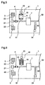
- Figure 7(a) is a plan view illustrating a prior art monolithic microwave semiconductor integrated circuit device.
- reference numeral 1 designates a semiconductor substrate comprising GaAs, Si, or the like
- numeral 3 designated via-holes
- numeral 4 designates a capacitor comprising a lamination of metal/insulator/metal (hereinafter referred to as MIM capacitor)
- numeral 7 designates a transistor, such as a field effect transistor
- numeral 21 designates an input electrode pad
- numeral 22 designates ground electrode pads
- numeral 23 designates a gate bias electrode pad
- numeral 24 designates a drain bias electrode pad
- numerals 51 and 52 designate signal transmission lines
- numeral 61 designates a gate side bias line
- numeral 62 designates a drain side bias line.
- an oscillation preventing circuit 11 including an MIM capacitor 41 connected to the bias line 61 is included in the IC device.
- the MIM capacitors 41 of the oscillation preventing circuits 11 corresponding to the respective transistors 7 it is necessary for the MIM capacitors 41 of the oscillation preventing circuits 11 corresponding to the respective transistors 7 to have different capacitances according to the different oscillation characteristics of the transistors 7.
- thermoplastic material layer is disposed on two regions of the substrate which are opposed each other with the bias line between them, and the magnetic substance layer is disposed across the bias line and adhered to and supported by the thermoplastic material layer. Therefore, as described above, the oscillation of the active element is easily prevented. Further, the unwanted increase in the chip area of the integrated circuit device due to the use of the prior art oscillation preventing circuit is avoided.
- thermoplastic material layer is disposed on a region of the substrate including a required region on the bias line. Therefore, as described above, the oscillation of the active element is easily prevented. Further, the unwanted increase in the chip area of the integrated circuit device due to the use of the prior art oscillation preventing circuit is avoided.
- the oscillation characteristics of the active element is evaluated by applying a DC bias voltage to the active element, and after the evaluation of the oscillation characteristics, the magnetic substance layer is formed in an appropriate shape and on an appropriate position according to the oscillation characteristics of the active element. Therefore, the oscillation of the active element is easily prevented. Further, since the magnetic substance layer is formed on the bias line, the unwanted increase in the chip area of the integrated circuit device due to the use of the prior art oscillation preventing circuit is avoided.
- Figure 1 is a plan view illustrating a monolithic microwave semiconductor IC device in accordance with a first embodiment of the present invention.
- the same reference numerals as those in figure 7(a) designate the same or corresponding parts.
- Reference numeral 8 designates thermoplastic polyimide layers and reference numeral 9 designates a magnetic substance layer.
- the MIM capacitor 4 connected between the input electrode pad 21 and the gate of the transistor 7 is permeable to microwave signals and impermeable to DC signals.
- the thermoplastic polyimide layers 8 are located on both sides of the gate side bias line 61.
- the magnetic substance layer 9 is adhered to the thermoplastic polyimide layers 8 across the gate side bias line 61, whereby the magnetic substance 9 is fixed to the semiconductor substrate 1.
- the magnetic substance layer 9 comprises thermoplastic polyimide containing ferrite grains, or ferrite in the shape of a plate or beads.
- Figure 2 is a plan view illustrating a process step in the fabricating method.
- the same reference numerals as in figure 1 designate the same or corresponding parts.
- the oscillation of the transistor 7 since the frequency components of the oscillation of the transistor 7 to which the DC bias voltage is applied are absorbed by the magnetic substance layer 9, the oscillation of the transistor 7 is prevented. Further, after the fabrication of the circuit elements, i.e., the transistor 7, the bias lines 61 and 62, the signal transmission lines 51 and 52, and the like on the semiconductor substrate 1, the transistor 7 is operated to evaluate the oscillation characteristics and, thereafter, the magnetic substance layer 9 is formed across the gate side bias line 61. Therefore, the shape and the position of the magnetic substance layer 9 can be appropriately selected according to the oscillation characteristics of the transistor 7, so that the oscillation of any transistor can be easily prevented.
- the magnetic substance layer 9 is disposed on the gate side bias line 61, it may be disposed on the drain side bias line 62 or on both of these bias lines. Alternatively, a plurality of magnetic substance layers may be adhered to the thermoplastic polyimide layers 8.
- Figure 3 is a plan view illustrating a monolithic microwave semiconductor IC device in accordance with a second embodiment of the present invention.
- the same reference numerals as those in figure 1 designate the same or corresponding parts.
- Figure 4 is a plan view illustrating a process step in the fabricating method.
- the same reference numerals as in figure 3 designate the same or corresponding parts.
- the IC device shown in figure 3 on which the magnetic substance layers 9 for preventing oscillation of the transistor 7 are disposed across the drain side bias line 62 is fabricated.
- thermoplastic polyimide layer 8 Although two magnetic substances layers are adhered to the thermoplastic polyimide layer 8, a single magnetic substance layer or three or more magnetic substance layers may be adhered.
- thermoplastic polyimide patterns 10 are disposed on the semiconductor substrate 1 at the both sides of the gate side bias line 61.
- the magnetic substance layer 9 comprising thermoplastic polyimide containing ferrite grains, or ferrite in the shape of a plate or a bead is disposed across the bias line 61 and adhered to the thermoplastic polyimide patterns 10, whereby it is fixed to the semiconductor substrate 1. While in the above-described first and second embodiments a plate-shaped thermoplastic polyimide layer is employed, in this third embodiment a plurality of island patterns of thermoplastic polyimide are employed.
- the via-holes 3, the MIM capacitor 4, the transistor 7, the electrode pads 21 to 24, the signal transmission lines 51 and 52, and the bias lines 61 and 62 are fabricated on the semiconductor substrate 1.
- the thermoplastic polyimide patterns 10 are formed on the semiconductor substrate 1 at the both sides of the bias line 61 as shown in figure 6.
- DC bias voltage is applied to the gate and the drain of the transistor 7 to evaluate the oscillation characteristics of the transistor 7.
- thermoplastic polyimide patterns 10 Although a single magnetic substance layer is adhered to the thermoplastic polyimide patterns 10, a plurality of magnetic substance layers may be adhered.
Landscapes
- Engineering & Computer Science (AREA)
- Power Engineering (AREA)
- Semiconductor Integrated Circuits (AREA)
- Junction Field-Effect Transistors (AREA)
- Waveguide Connection Structure (AREA)
- Microwave Amplifiers (AREA)
Applications Claiming Priority (3)
| Application Number | Priority Date | Filing Date | Title |
|---|---|---|---|
| JP7080221A JPH08279596A (ja) | 1995-04-05 | 1995-04-05 | 集積回路装置,及びその製造方法 |
| JP8022195 | 1995-04-05 | ||
| EP96100652A EP0736902B1 (fr) | 1995-04-05 | 1996-01-17 | Dispositif à circuit intégré et procédé de fabrication |
Related Parent Applications (1)
| Application Number | Title | Priority Date | Filing Date |
|---|---|---|---|
| EP96100652.5 Division | 1996-01-17 |
Publications (1)
| Publication Number | Publication Date |
|---|---|
| EP1059666A1 true EP1059666A1 (fr) | 2000-12-13 |
Family
ID=13712321
Family Applications (2)
| Application Number | Title | Priority Date | Filing Date |
|---|---|---|---|
| EP00117641A Withdrawn EP1059666A1 (fr) | 1995-04-05 | 1996-01-17 | Dispositif à circuit intégré à semiconducteur monolithique |
| EP96100652A Expired - Lifetime EP0736902B1 (fr) | 1995-04-05 | 1996-01-17 | Dispositif à circuit intégré et procédé de fabrication |
Family Applications After (1)
| Application Number | Title | Priority Date | Filing Date |
|---|---|---|---|
| EP96100652A Expired - Lifetime EP0736902B1 (fr) | 1995-04-05 | 1996-01-17 | Dispositif à circuit intégré et procédé de fabrication |
Country Status (4)
| Country | Link |
|---|---|
| US (1) | US5675184A (fr) |
| EP (2) | EP1059666A1 (fr) |
| JP (1) | JPH08279596A (fr) |
| DE (1) | DE69615437T2 (fr) |
Families Citing this family (35)
| Publication number | Priority date | Publication date | Assignee | Title |
|---|---|---|---|---|
| JPH08288452A (ja) * | 1995-04-20 | 1996-11-01 | Mitsubishi Electric Corp | 集積回路装置,及びその製造方法 |
| JP3185918B2 (ja) * | 1996-08-05 | 2001-07-11 | 株式会社村田製作所 | 電子装置 |
| US6329234B1 (en) | 2000-07-24 | 2001-12-11 | Taiwan Semiconductor Manufactuirng Company | Copper process compatible CMOS metal-insulator-metal capacitor structure and its process flow |
| JP4804643B2 (ja) * | 2001-05-08 | 2011-11-02 | 三菱電機株式会社 | 高周波回路装置とその製造方法 |
| DE10162637C1 (de) * | 2001-12-20 | 2003-08-21 | Eupec Gmbh & Co Kg | Schaltungsanordnung mit elektronischen Bauelementen auf einem isolierenden Trägersubstrat |
| US7091542B1 (en) * | 2005-01-28 | 2006-08-15 | International Business Machines Corporation | Method of forming a MIM capacitor for Cu BEOL application |
| US20060197183A1 (en) * | 2005-03-01 | 2006-09-07 | International Business Machines Corporation | Improved mim capacitor structure and process |
| US7223654B2 (en) * | 2005-04-15 | 2007-05-29 | International Business Machines Corporation | MIM capacitor and method of fabricating same |
| US8728072B2 (en) | 2005-05-12 | 2014-05-20 | Aesculap Ag | Electrocautery method and apparatus |
| US9339323B2 (en) | 2005-05-12 | 2016-05-17 | Aesculap Ag | Electrocautery method and apparatus |
| US8696662B2 (en) | 2005-05-12 | 2014-04-15 | Aesculap Ag | Electrocautery method and apparatus |
| US7862565B2 (en) | 2005-05-12 | 2011-01-04 | Aragon Surgical, Inc. | Method for tissue cauterization |
| US8574229B2 (en) | 2006-05-02 | 2013-11-05 | Aesculap Ag | Surgical tool |
| JP5078471B2 (ja) * | 2007-07-06 | 2012-11-21 | 三菱電機株式会社 | 高周波増幅器 |
| US8870867B2 (en) | 2008-02-06 | 2014-10-28 | Aesculap Ag | Articulable electrosurgical instrument with a stabilizable articulation actuator |
| KR101580925B1 (ko) * | 2009-04-28 | 2015-12-30 | 삼성전자주식회사 | 칩온 보드 타입의 패키지 |
| KR101786410B1 (ko) | 2010-02-04 | 2017-10-17 | 아에스쿨랍 아게 | 복강경 고주파 수술장치 |
| US8827992B2 (en) | 2010-03-26 | 2014-09-09 | Aesculap Ag | Impedance mediated control of power delivery for electrosurgery |
| US8419727B2 (en) | 2010-03-26 | 2013-04-16 | Aesculap Ag | Impedance mediated power delivery for electrosurgery |
| US9173698B2 (en) | 2010-09-17 | 2015-11-03 | Aesculap Ag | Electrosurgical tissue sealing augmented with a seal-enhancing composition |
| US8405135B2 (en) | 2010-10-05 | 2013-03-26 | International Business Machines Corporation | 3D via capacitor with a floating conductive plate for improved reliability |
| US9339327B2 (en) | 2011-06-28 | 2016-05-17 | Aesculap Ag | Electrosurgical tissue dissecting device |
| CN107252348B (zh) | 2012-09-26 | 2019-12-27 | 蛇牌股份公司 | 用于组织切割和封合的设备 |
| US8901711B1 (en) | 2013-08-07 | 2014-12-02 | International Business Machines Corporation | Horizontal metal-insulator-metal capacitor |
| US10090240B2 (en) | 2016-06-03 | 2018-10-02 | Globalfoundries Inc. | Interconnect structure with capacitor element and related methods |
| US9875959B2 (en) | 2016-06-09 | 2018-01-23 | International Business Machines Corporation | Forming a stacked capacitor |
| US10032711B2 (en) | 2016-07-25 | 2018-07-24 | International Business Machines Corporation | Integrating metal-insulator-metal capacitors with air gap process flow |
| US9893144B1 (en) | 2016-08-05 | 2018-02-13 | International Business Machines Corporation | Methods for fabricating metal-insulator-metal capacitors |
| US9698213B1 (en) | 2016-09-28 | 2017-07-04 | International Business Machines Corporation | Vertical MIM capacitor |
| US9876068B1 (en) | 2016-10-31 | 2018-01-23 | International Business Machines Corporation | High-K metal-insulator-metal capacitor and method of manufacturing the same |
| US10008558B1 (en) | 2017-01-05 | 2018-06-26 | International Business Machines Corporation | Advanced metal insulator metal capacitor |
| US10032855B1 (en) | 2017-01-05 | 2018-07-24 | International Business Machines Corporation | Advanced metal insulator metal capacitor |
| US10090378B1 (en) | 2017-03-17 | 2018-10-02 | International Business Machines Corporation | Efficient metal-insulator-metal capacitor |
| US11031457B2 (en) | 2017-12-15 | 2021-06-08 | International Business Machines Corporation | Low resistance high capacitance density MIM capacitor |
| US10497519B1 (en) | 2018-09-27 | 2019-12-03 | International Business Machines Corporation | Back-end-of-the line capacitor |
Citations (6)
| Publication number | Priority date | Publication date | Assignee | Title |
|---|---|---|---|---|
| JPS5797201A (en) * | 1980-12-09 | 1982-06-16 | Fujitsu Ltd | Integrated circuit for microwave |
| EP0169694A2 (fr) * | 1984-07-25 | 1986-01-29 | Rca Licensing Corporation | Composant supprimant de signaux à haute fréquence |
| US4716389A (en) * | 1986-10-20 | 1987-12-29 | Honeywell Inc. | Millimeter wave microstrip surface mounted attenuator |
| JPH0352302A (ja) * | 1989-07-19 | 1991-03-06 | Sanyo Electric Co Ltd | モノリシックマイクロ波集積回路 |
| JPH05235655A (ja) * | 1992-02-19 | 1993-09-10 | Toshiba Lighting & Technol Corp | 高周波用増幅回路 |
| JPH08204471A (ja) * | 1995-01-20 | 1996-08-09 | Mitsubishi Electric Corp | 高周波増幅器およびその発振防止方法 |
Family Cites Families (4)
| Publication number | Priority date | Publication date | Assignee | Title |
|---|---|---|---|---|
| US3959874A (en) * | 1974-12-20 | 1976-06-01 | Western Electric Company, Inc. | Method of forming an integrated circuit assembly |
| US5019535A (en) * | 1989-03-28 | 1991-05-28 | General Electric Company | Die attachment method using nonconductive adhesive for use in high density interconnected assemblies |
| US5138431A (en) * | 1990-01-31 | 1992-08-11 | Vlsi Technology, Inc. | Lead and socket structures with reduced self-inductance |
| US5469334A (en) * | 1991-09-09 | 1995-11-21 | Power Integrations, Inc. | Plastic quad-packaged switched-mode integrated circuit with integrated transformer windings and mouldings for transformer core pieces |
-
1995
- 1995-04-05 JP JP7080221A patent/JPH08279596A/ja active Pending
-
1996
- 1996-01-17 US US08/587,527 patent/US5675184A/en not_active Expired - Fee Related
- 1996-01-17 EP EP00117641A patent/EP1059666A1/fr not_active Withdrawn
- 1996-01-17 DE DE69615437T patent/DE69615437T2/de not_active Expired - Fee Related
- 1996-01-17 EP EP96100652A patent/EP0736902B1/fr not_active Expired - Lifetime
Patent Citations (6)
| Publication number | Priority date | Publication date | Assignee | Title |
|---|---|---|---|---|
| JPS5797201A (en) * | 1980-12-09 | 1982-06-16 | Fujitsu Ltd | Integrated circuit for microwave |
| EP0169694A2 (fr) * | 1984-07-25 | 1986-01-29 | Rca Licensing Corporation | Composant supprimant de signaux à haute fréquence |
| US4716389A (en) * | 1986-10-20 | 1987-12-29 | Honeywell Inc. | Millimeter wave microstrip surface mounted attenuator |
| JPH0352302A (ja) * | 1989-07-19 | 1991-03-06 | Sanyo Electric Co Ltd | モノリシックマイクロ波集積回路 |
| JPH05235655A (ja) * | 1992-02-19 | 1993-09-10 | Toshiba Lighting & Technol Corp | 高周波用増幅回路 |
| JPH08204471A (ja) * | 1995-01-20 | 1996-08-09 | Mitsubishi Electric Corp | 高周波増幅器およびその発振防止方法 |
Non-Patent Citations (4)
| Title |
|---|
| PATENT ABSTRACTS OF JAPAN vol. 006, no. 182 (E - 131) 18 September 1982 (1982-09-18) * |
| PATENT ABSTRACTS OF JAPAN vol. 015, no. 195 (E - 1069) 20 May 1991 (1991-05-20) * |
| PATENT ABSTRACTS OF JAPAN vol. 017, no. 691 (E - 1479) 17 December 1993 (1993-12-17) * |
| PATENT ABSTRACTS OF JAPAN vol. 1996, no. 12 26 December 1996 (1996-12-26) * |
Also Published As
| Publication number | Publication date |
|---|---|
| EP0736902B1 (fr) | 2001-09-26 |
| JPH08279596A (ja) | 1996-10-22 |
| US5675184A (en) | 1997-10-07 |
| DE69615437D1 (de) | 2001-10-31 |
| DE69615437T2 (de) | 2002-07-11 |
| EP0736902A2 (fr) | 1996-10-09 |
| EP0736902A3 (fr) | 1997-10-29 |
Similar Documents
| Publication | Publication Date | Title |
|---|---|---|
| US5675184A (en) | Integrated circuit device | |
| US5635762A (en) | Flip chip semiconductor device with dual purpose metallized ground conductor | |
| US7323770B2 (en) | Hybrid integrated circuit device, and method for fabricating the same, and electronic device | |
| US6301122B1 (en) | Radio frequency module with thermally and electrically coupled metal film on insulating substrate | |
| EP0680141B1 (fr) | Améliorations de la caractéristique de fréquence d'un dispositif semi-conducteur dans la bande des micro-ondes | |
| KR100394249B1 (ko) | 집적 반도체에서의 테스트 구조물 | |
| US6710426B2 (en) | Semiconductor device and transceiver apparatus | |
| US20030151113A1 (en) | Semiconductor device | |
| JP3328542B2 (ja) | 高周波半導体集積回路装置 | |
| US5786627A (en) | Integrated circuit device and fabricating thereof | |
| JPH01173761A (ja) | 高周波用トランジスタ | |
| JPH04113653A (ja) | 半導体装置 | |
| JPH10126032A (ja) | 表面実装部品の実装構造及び実装方法 | |
| JP2674546B2 (ja) | ビームリード型半導体装置の製造方法 | |
| JPH04371003A (ja) | マイクロ波集積回路装置 | |
| JP2802375B2 (ja) | 電気素子・光素子混載回路の周波数特性伸張法 | |
| JPH0786612A (ja) | モノリシック半導体デバイス | |
| JPH1075146A (ja) | ノイズフィルタ | |
| JPH0443416B2 (fr) | ||
| JPH03145141A (ja) | 半導体装置 | |
| GB2283856A (en) | Method of adjusting operating characteristics of microwave components | |
| JPS6350106A (ja) | 高周波半導体装置 | |
| JP2000223501A (ja) | 半導体集積回路装置とその製造方法 | |
| JPH02105701A (ja) | マイクロ波集積回路用バイアス回路 | |
| JPH0318339B2 (fr) |
Legal Events
| Date | Code | Title | Description |
|---|---|---|---|
| PUAI | Public reference made under article 153(3) epc to a published international application that has entered the european phase |
Free format text: ORIGINAL CODE: 0009012 |
|
| AC | Divisional application: reference to earlier application |
Ref document number: 736902 Country of ref document: EP |
|
| AK | Designated contracting states |
Kind code of ref document: A1 Designated state(s): DE FR GB |
|
| RIN1 | Information on inventor provided before grant (corrected) |
Inventor name: OHTA, YUKIO Inventor name: NOTANI, YOSHIHIRO Inventor name: GOTO, KEI Inventor name: MATSUBAYASHI, HIROTO |
|
| 17P | Request for examination filed |
Effective date: 20010611 |
|
| AKX | Designation fees paid |
Free format text: DE FR GB |
|
| 17Q | First examination report despatched |
Effective date: 20020412 |
|
| RAP1 | Party data changed (applicant data changed or rights of an application transferred) |
Owner name: MITSUBISHI DENKI KABUSHIKI KAISHA |
|
| STAA | Information on the status of an ep patent application or granted ep patent |
Free format text: STATUS: THE APPLICATION HAS BEEN WITHDRAWN |
|
| 18W | Application withdrawn |
Effective date: 20061027 |