EP1453159B1 - Structure d'un dispositif emettant de la lumiere a couche monocristalline non epitaxiee de nitrure - Google Patents
Structure d'un dispositif emettant de la lumiere a couche monocristalline non epitaxiee de nitrure Download PDFInfo
- Publication number
- EP1453159B1 EP1453159B1 EP02803072.4A EP02803072A EP1453159B1 EP 1453159 B1 EP1453159 B1 EP 1453159B1 EP 02803072 A EP02803072 A EP 02803072A EP 1453159 B1 EP1453159 B1 EP 1453159B1
- Authority
- EP
- European Patent Office
- Prior art keywords
- layer
- gallium
- light emitting
- substrate
- emitting device
- Prior art date
- Legal status (The legal status is an assumption and is not a legal conclusion. Google has not performed a legal analysis and makes no representation as to the accuracy of the status listed.)
- Expired - Lifetime
Links
Images


Classifications
-
- C—CHEMISTRY; METALLURGY
- C30—CRYSTAL GROWTH
- C30B—SINGLE-CRYSTAL GROWTH; UNIDIRECTIONAL SOLIDIFICATION OF EUTECTIC MATERIAL OR UNIDIRECTIONAL DEMIXING OF EUTECTOID MATERIAL; REFINING BY ZONE-MELTING OF MATERIAL; PRODUCTION OF A HOMOGENEOUS POLYCRYSTALLINE MATERIAL WITH DEFINED STRUCTURE; SINGLE CRYSTALS OR HOMOGENEOUS POLYCRYSTALLINE MATERIAL WITH DEFINED STRUCTURE; AFTER-TREATMENT OF SINGLE CRYSTALS OR A HOMOGENEOUS POLYCRYSTALLINE MATERIAL WITH DEFINED STRUCTURE; APPARATUS THEREFOR
- C30B29/00—Single crystals or homogeneous polycrystalline material with defined structure characterised by the material or by their shape
- C30B29/10—Inorganic compounds or compositions
- C30B29/40—AIIIBV compounds wherein A is B, Al, Ga, In or Tl and B is N, P, As, Sb or Bi
- C30B29/403—AIII-nitrides
-
- H—ELECTRICITY
- H01—ELECTRIC ELEMENTS
- H01S—DEVICES USING THE PROCESS OF LIGHT AMPLIFICATION BY STIMULATED EMISSION OF RADIATION [LASER] TO AMPLIFY OR GENERATE LIGHT; DEVICES USING STIMULATED EMISSION OF ELECTROMAGNETIC RADIATION IN WAVE RANGES OTHER THAN OPTICAL
- H01S5/00—Semiconductor lasers
- H01S5/30—Structure or shape of the active region; Materials used for the active region
-
- B—PERFORMING OPERATIONS; TRANSPORTING
- B82—NANOTECHNOLOGY
- B82Y—SPECIFIC USES OR APPLICATIONS OF NANOSTRUCTURES; MEASUREMENT OR ANALYSIS OF NANOSTRUCTURES; MANUFACTURE OR TREATMENT OF NANOSTRUCTURES
- B82Y20/00—Nanooptics, e.g. quantum optics or photonic crystals
-
- C—CHEMISTRY; METALLURGY
- C30—CRYSTAL GROWTH
- C30B—SINGLE-CRYSTAL GROWTH; UNIDIRECTIONAL SOLIDIFICATION OF EUTECTIC MATERIAL OR UNIDIRECTIONAL DEMIXING OF EUTECTOID MATERIAL; REFINING BY ZONE-MELTING OF MATERIAL; PRODUCTION OF A HOMOGENEOUS POLYCRYSTALLINE MATERIAL WITH DEFINED STRUCTURE; SINGLE CRYSTALS OR HOMOGENEOUS POLYCRYSTALLINE MATERIAL WITH DEFINED STRUCTURE; AFTER-TREATMENT OF SINGLE CRYSTALS OR A HOMOGENEOUS POLYCRYSTALLINE MATERIAL WITH DEFINED STRUCTURE; APPARATUS THEREFOR
- C30B29/00—Single crystals or homogeneous polycrystalline material with defined structure characterised by the material or by their shape
- C30B29/10—Inorganic compounds or compositions
- C30B29/40—AIIIBV compounds wherein A is B, Al, Ga, In or Tl and B is N, P, As, Sb or Bi
- C30B29/403—AIII-nitrides
- C30B29/406—Gallium nitride
-
- C—CHEMISTRY; METALLURGY
- C30—CRYSTAL GROWTH
- C30B—SINGLE-CRYSTAL GROWTH; UNIDIRECTIONAL SOLIDIFICATION OF EUTECTIC MATERIAL OR UNIDIRECTIONAL DEMIXING OF EUTECTOID MATERIAL; REFINING BY ZONE-MELTING OF MATERIAL; PRODUCTION OF A HOMOGENEOUS POLYCRYSTALLINE MATERIAL WITH DEFINED STRUCTURE; SINGLE CRYSTALS OR HOMOGENEOUS POLYCRYSTALLINE MATERIAL WITH DEFINED STRUCTURE; AFTER-TREATMENT OF SINGLE CRYSTALS OR A HOMOGENEOUS POLYCRYSTALLINE MATERIAL WITH DEFINED STRUCTURE; APPARATUS THEREFOR
- C30B7/00—Single-crystal growth from solutions using solvents which are liquid at normal temperature, e.g. aqueous solutions
- C30B7/005—Epitaxial layer growth
-
- C—CHEMISTRY; METALLURGY
- C30—CRYSTAL GROWTH
- C30B—SINGLE-CRYSTAL GROWTH; UNIDIRECTIONAL SOLIDIFICATION OF EUTECTIC MATERIAL OR UNIDIRECTIONAL DEMIXING OF EUTECTOID MATERIAL; REFINING BY ZONE-MELTING OF MATERIAL; PRODUCTION OF A HOMOGENEOUS POLYCRYSTALLINE MATERIAL WITH DEFINED STRUCTURE; SINGLE CRYSTALS OR HOMOGENEOUS POLYCRYSTALLINE MATERIAL WITH DEFINED STRUCTURE; AFTER-TREATMENT OF SINGLE CRYSTALS OR A HOMOGENEOUS POLYCRYSTALLINE MATERIAL WITH DEFINED STRUCTURE; APPARATUS THEREFOR
- C30B7/00—Single-crystal growth from solutions using solvents which are liquid at normal temperature, e.g. aqueous solutions
- C30B7/10—Single-crystal growth from solutions using solvents which are liquid at normal temperature, e.g. aqueous solutions by application of pressure, e.g. hydrothermal processes
-
- C—CHEMISTRY; METALLURGY
- C30—CRYSTAL GROWTH
- C30B—SINGLE-CRYSTAL GROWTH; UNIDIRECTIONAL SOLIDIFICATION OF EUTECTIC MATERIAL OR UNIDIRECTIONAL DEMIXING OF EUTECTOID MATERIAL; REFINING BY ZONE-MELTING OF MATERIAL; PRODUCTION OF A HOMOGENEOUS POLYCRYSTALLINE MATERIAL WITH DEFINED STRUCTURE; SINGLE CRYSTALS OR HOMOGENEOUS POLYCRYSTALLINE MATERIAL WITH DEFINED STRUCTURE; AFTER-TREATMENT OF SINGLE CRYSTALS OR A HOMOGENEOUS POLYCRYSTALLINE MATERIAL WITH DEFINED STRUCTURE; APPARATUS THEREFOR
- C30B9/00—Single-crystal growth from melt solutions using molten solvents
-
- H—ELECTRICITY
- H01—ELECTRIC ELEMENTS
- H01S—DEVICES USING THE PROCESS OF LIGHT AMPLIFICATION BY STIMULATED EMISSION OF RADIATION [LASER] TO AMPLIFY OR GENERATE LIGHT; DEVICES USING STIMULATED EMISSION OF ELECTROMAGNETIC RADIATION IN WAVE RANGES OTHER THAN OPTICAL
- H01S5/00—Semiconductor lasers
- H01S5/10—Construction or shape of the optical resonator, e.g. extended or external cavity, coupled cavities, bent-guide, varying width, thickness or composition of the active region
- H01S5/16—Window-type lasers, i.e. with a region of non-absorbing material between the active region and the reflecting surface
- H01S5/164—Window-type lasers, i.e. with a region of non-absorbing material between the active region and the reflecting surface with window regions comprising semiconductor material with a wider bandgap than the active layer
-
- H—ELECTRICITY
- H01—ELECTRIC ELEMENTS
- H01S—DEVICES USING THE PROCESS OF LIGHT AMPLIFICATION BY STIMULATED EMISSION OF RADIATION [LASER] TO AMPLIFY OR GENERATE LIGHT; DEVICES USING STIMULATED EMISSION OF ELECTROMAGNETIC RADIATION IN WAVE RANGES OTHER THAN OPTICAL
- H01S5/00—Semiconductor lasers
- H01S5/30—Structure or shape of the active region; Materials used for the active region
- H01S5/32—Structure or shape of the active region; Materials used for the active region comprising PN junctions, e.g. hetero- or double- heterostructures
- H01S5/3202—Structure or shape of the active region; Materials used for the active region comprising PN junctions, e.g. hetero- or double- heterostructures grown on specifically orientated substrates, or using orientation dependent growth
- H01S5/32025—Structure or shape of the active region; Materials used for the active region comprising PN junctions, e.g. hetero- or double- heterostructures grown on specifically orientated substrates, or using orientation dependent growth non-polar orientation
-
- H—ELECTRICITY
- H01—ELECTRIC ELEMENTS
- H01S—DEVICES USING THE PROCESS OF LIGHT AMPLIFICATION BY STIMULATED EMISSION OF RADIATION [LASER] TO AMPLIFY OR GENERATE LIGHT; DEVICES USING STIMULATED EMISSION OF ELECTROMAGNETIC RADIATION IN WAVE RANGES OTHER THAN OPTICAL
- H01S2304/00—Special growth methods for semiconductor lasers
- H01S2304/12—Pendeo epitaxial lateral overgrowth [ELOG], e.g. for growing GaN based blue laser diodes
-
- H—ELECTRICITY
- H01—ELECTRIC ELEMENTS
- H01S—DEVICES USING THE PROCESS OF LIGHT AMPLIFICATION BY STIMULATED EMISSION OF RADIATION [LASER] TO AMPLIFY OR GENERATE LIGHT; DEVICES USING STIMULATED EMISSION OF ELECTROMAGNETIC RADIATION IN WAVE RANGES OTHER THAN OPTICAL
- H01S5/00—Semiconductor lasers
- H01S5/02—Structural details or components not essential to laser action
- H01S5/0206—Substrates, e.g. growth, shape, material, removal or bonding
- H01S5/021—Silicon based substrates
-
- H—ELECTRICITY
- H01—ELECTRIC ELEMENTS
- H01S—DEVICES USING THE PROCESS OF LIGHT AMPLIFICATION BY STIMULATED EMISSION OF RADIATION [LASER] TO AMPLIFY OR GENERATE LIGHT; DEVICES USING STIMULATED EMISSION OF ELECTROMAGNETIC RADIATION IN WAVE RANGES OTHER THAN OPTICAL
- H01S5/00—Semiconductor lasers
- H01S5/02—Structural details or components not essential to laser action
- H01S5/0206—Substrates, e.g. growth, shape, material, removal or bonding
- H01S5/0213—Sapphire, quartz or diamond based substrates
-
- H—ELECTRICITY
- H01—ELECTRIC ELEMENTS
- H01S—DEVICES USING THE PROCESS OF LIGHT AMPLIFICATION BY STIMULATED EMISSION OF RADIATION [LASER] TO AMPLIFY OR GENERATE LIGHT; DEVICES USING STIMULATED EMISSION OF ELECTROMAGNETIC RADIATION IN WAVE RANGES OTHER THAN OPTICAL
- H01S5/00—Semiconductor lasers
- H01S5/02—Structural details or components not essential to laser action
- H01S5/0206—Substrates, e.g. growth, shape, material, removal or bonding
- H01S5/0218—Substrates comprising semiconducting materials from other groups of the Periodic Table than the materials of the active layer
-
- H—ELECTRICITY
- H01—ELECTRIC ELEMENTS
- H01S—DEVICES USING THE PROCESS OF LIGHT AMPLIFICATION BY STIMULATED EMISSION OF RADIATION [LASER] TO AMPLIFY OR GENERATE LIGHT; DEVICES USING STIMULATED EMISSION OF ELECTROMAGNETIC RADIATION IN WAVE RANGES OTHER THAN OPTICAL
- H01S5/00—Semiconductor lasers
- H01S5/02—Structural details or components not essential to laser action
- H01S5/028—Coatings ; Treatment of the laser facets, e.g. etching, passivation layers or reflecting layers
- H01S5/0281—Coatings made of semiconductor materials
-
- H—ELECTRICITY
- H01—ELECTRIC ELEMENTS
- H01S—DEVICES USING THE PROCESS OF LIGHT AMPLIFICATION BY STIMULATED EMISSION OF RADIATION [LASER] TO AMPLIFY OR GENERATE LIGHT; DEVICES USING STIMULATED EMISSION OF ELECTROMAGNETIC RADIATION IN WAVE RANGES OTHER THAN OPTICAL
- H01S5/00—Semiconductor lasers
- H01S5/20—Structure or shape of the semiconductor body to guide the optical wave ; Confining structures perpendicular to the optical axis, e.g. index or gain guiding, stripe geometry, broad area lasers, gain tailoring, transverse or lateral reflectors, special cladding structures, MQW barrier reflection layers
- H01S5/22—Structure or shape of the semiconductor body to guide the optical wave ; Confining structures perpendicular to the optical axis, e.g. index or gain guiding, stripe geometry, broad area lasers, gain tailoring, transverse or lateral reflectors, special cladding structures, MQW barrier reflection layers having a ridge or stripe structure
-
- H—ELECTRICITY
- H01—ELECTRIC ELEMENTS
- H01S—DEVICES USING THE PROCESS OF LIGHT AMPLIFICATION BY STIMULATED EMISSION OF RADIATION [LASER] TO AMPLIFY OR GENERATE LIGHT; DEVICES USING STIMULATED EMISSION OF ELECTROMAGNETIC RADIATION IN WAVE RANGES OTHER THAN OPTICAL
- H01S5/00—Semiconductor lasers
- H01S5/30—Structure or shape of the active region; Materials used for the active region
- H01S5/32—Structure or shape of the active region; Materials used for the active region comprising PN junctions, e.g. hetero- or double- heterostructures
- H01S5/323—Structure or shape of the active region; Materials used for the active region comprising PN junctions, e.g. hetero- or double- heterostructures in AIIIBV compounds, e.g. AlGaAs-laser, InP-based laser
- H01S5/32308—Structure or shape of the active region; Materials used for the active region comprising PN junctions, e.g. hetero- or double- heterostructures in AIIIBV compounds, e.g. AlGaAs-laser, InP-based laser emitting light at a wavelength less than 900 nm
- H01S5/32341—Structure or shape of the active region; Materials used for the active region comprising PN junctions, e.g. hetero- or double- heterostructures in AIIIBV compounds, e.g. AlGaAs-laser, InP-based laser emitting light at a wavelength less than 900 nm blue laser based on GaN or GaP
-
- H—ELECTRICITY
- H01—ELECTRIC ELEMENTS
- H01S—DEVICES USING THE PROCESS OF LIGHT AMPLIFICATION BY STIMULATED EMISSION OF RADIATION [LASER] TO AMPLIFY OR GENERATE LIGHT; DEVICES USING STIMULATED EMISSION OF ELECTROMAGNETIC RADIATION IN WAVE RANGES OTHER THAN OPTICAL
- H01S5/00—Semiconductor lasers
- H01S5/30—Structure or shape of the active region; Materials used for the active region
- H01S5/34—Structure or shape of the active region; Materials used for the active region comprising quantum well or superlattice structures, e.g. single quantum well [SQW] lasers, multiple quantum well [MQW] lasers or graded index separate confinement heterostructure [GRINSCH] lasers
- H01S5/343—Structure or shape of the active region; Materials used for the active region comprising quantum well or superlattice structures, e.g. single quantum well [SQW] lasers, multiple quantum well [MQW] lasers or graded index separate confinement heterostructure [GRINSCH] lasers in AIIIBV compounds, e.g. AlGaAs-laser, InP-based laser
- H01S5/34333—Structure or shape of the active region; Materials used for the active region comprising quantum well or superlattice structures, e.g. single quantum well [SQW] lasers, multiple quantum well [MQW] lasers or graded index separate confinement heterostructure [GRINSCH] lasers in AIIIBV compounds, e.g. AlGaAs-laser, InP-based laser with a well layer based on Ga(In)N or Ga(In)P, e.g. blue laser
Definitions
- This invention relates to a manufacturing method of a light emitting device structure wherein a single crystal nitride layer prepared by a supercritical ammonia method is used as a substrate.
- the dislocation density in the waveguide should be 10 4 /cm 2 or less.
- the dislocation density can not be reduced less than 10 6 /cm 2 by using a vapor phase epitaxial growth (MOCVD and HVPE) or by using a repeated ELOG (Epitaxial lateral overgrowth) because the waveguide is grown on a heterogeneous substrate, such as sapphire substrate or SiC substrate.
- the thickness of the epitaxial layer should be 100 ⁇ or less to form the epitaxial layer on a sapphire substrate or a SiC layer without crack by the vapor phase growth.
- a nitride crystal is formed on C-plane as an epitaxial growth face on the heterogeneous substrate such as the SiC substrate or the sapphire substrate by a vapor phase growth, which leads the active layer of the laser structure formed thereon to have a spontaneous polarization or piezo polarization causing a deterioration of the performance such as red shift of light emitting, recombination degradation and increase of the threshold current.
- the active layer deposited on the heterogeneous substrate is formed by a quantum well layer containing In
- the active layer is influenced by the crystal condition of the n-type nitride layer as a base, therefore it is necessary to form an undoped GaN layer or super lattice structure layer as the base.
- a protective layer is preferably formed to avoid the active layer degradation by evaporation of In therefrom.
- the protective layer for GaN or AlGaN layer is formed, the protective layer is formed at a temperature from 800°C to 900°C which is lower than that at formation of the active layer. Accordingly, a resultant nitride layer will be in the form of amorphous, which influences the crystal condition of the optical guide layer and p-type clad layer formed thereon.
- EP 0 716 457 A2 discloses a nitride semiconductor light-emitting device which has an active layer of a single-quantum well structure or multi-quantum well made of a nitride semiconductor containing indium and gallium.
- US 2001/0022154 A1 discloses a method and apparatus for homoepitaxial growth of freestanding, single bulk crystal Gallium Nitride (GaN), wherein a step of nucleating GaN in a reactor results in a GaN nucleation layer having a thickness of a few monolayers. The nucleation layer is stabilized, and a single bulk crystal GaN is grown from gas phase reactants on the GaN nucleation layer.
- GaN Gallium Nitride
- the first object of this invention is to form a nitride substrate having a lower dislocation density, i.e. 10 5 /cm 2 or less and more preferably 10 4 /cm 2 or less by using a supercritical ammonia technology instead of the so-far used vapor phase growth technology and to form thereon a laser structure having less crystal dislocation causing non-radiative recombination.
- the second object of this invention is to provide a laser device not influenced by the polarization, that is, to form a laser structure on non-polar nitride A-plane substrate or non-polar M-plane substrate by obtaining a nitride bulk single crystal layer in a supercritical condition instead of a vapor phase growth.
- the third object of this invention is to provide a light emitting device structure wherein especially intermediate layers influencing the crystalline of the active layer are prepared by a supercritical ammonia method instead of a vapor phase growth method so that there can be obtained the intermediate layers having lower crystal dislocation which can not be obtained by a vapor phase growth.
- the present invention provides a manufacturing method of a light emitting device structure as defined in the claims.
- a light emitting device structure comprising a gallium-containing nitride single crystal substrate, and an n-type gallium-containing nitride semiconductor layer or layers, a gallium-containing nitride semiconductor active layer and a p-type gallium-containing nitride semiconductor layer or layers by a vapor phase growth on the substrate, wherein the single crystal substrate is obtained from a gallium-containing nitride bulk single crystal, and provided with an epitaxial growth face with dislocation density of 10 5 /cm 2 or less.
- the crystal dislocation of the epitaxial growth face of the substrate according to the present invention can be reduced compared with those obtained by the so-far vapor phase growth, especially ELOG method, due to which the epitaxial layer formed thereon has a good crystalline quality without formation of a lower temperature buffer layer and the excellent device structure can be formed.
- a gallium-containing nitride single crystal substrate means not only a substrate wholly formed by a gallium-containing nitride but also a composite substrate (template) in which a gallium-containing nitride is grown on a heterogeneous substrate.
- the gallium-containing nitride is formed on the heterogeneous substrate in the supercritical ammonia by applying the method which comprises preforming GaN, AlN or AlGaN layer on the heterogeneous substrate and then forming the gallium-containing nitride thereon.
- a light emitting device structure comprising a gallium-containing nitride single crystal substrate, and an n-type gallium-containing nitride semiconductor layer or layers, a gallium-containing nitride semiconductor active layer and a p-type gallium-containing nitride semiconductor layer or layers by a vapor phase growth on the substrate, wherein the single crystal substrate is obtained from a gallium-containing nitride bulk single crystal, and provided with A-plane or M-plane ( Fig. 5 ) which is parallel to c-axis of hexagonal structure for an epitaxial growth, and wherein the n-type semiconductor layer or layers are formed directly or through Al(Ga)N buffer layer on A-plane or M-plane.
- a nitride bulk single crystal shown in Drawings can be prepared by applying AMMONO method, therefore A-plane or M-plane which is parallel to c-axis of hexagonal structure for an epitaxial growth can be obtained.
- Fig. 5 In the present situation, an epitaxial growth required by a device structure can be carried out since the plane has the area of 100 mm 2 .
- A-plane and M-plane has non-polar, differently from C-plane, therefore there can be obtained the laser device having no cause of the deterioration of the performance such as the red shift of light emitting, recombination degradation and increase of the threshold current.
- the substrate is A-plane or M-plane of the gallium-containing nitride and further the dislocation density of the substrate is preferably 10 5 /cm 2 or less.
- epitaxial layer is formed on the one side of the gallium-containing nitride single crystal substrate.
- the light emitting device can be formed by growing the epitaxial layer on both sides of the substrate so that undoped GaN, AlN or AlGaN layer prepared by AMMONO method can be used as an intermediate layer.
- a nitride light emitting device which comprises an n-type nitride semiconductor layer or layers, a p-type nitride semiconductor layer or layers and a nitride active layer containing In therebetween is characterized in that at least an n-type nitride semiconductor layer or layers containing n-type purities are formed on one side of the nitride bulk single crystal substrate, the nitride active layer and a p-type nitride semiconductor layer or layers are formed directly or through an n-type nitride semiconductor layer or layers on the other side of the nitride bulk single crystal.
- the substrate is intermediate layer of the device.
- the crystal dislocation of the substrate prepared by AMMONO method is remarkably reduced, due to which the active layer can be formed directly or through an n-type semiconductor layer or layers, for example an n-type clad layer or an n-type guide layer, differently from the conventional active layer formed through an n-type buffer layer, an undoped GaN layer, an n-type superlattice layer etc. This leads to improve the crystal quality of the active layer.
- the polarization influence in the active layer can be eliminated by using the substrate formed on A-plane or M-plane.
- the use of the nitride bulk single crystal layer prepared by AMMONO method as an intermediate layer is also described. Further, the intermediate layer can directly be prepared by AMMONO method. Also described is that
- GaN or AlGaN single crystal layer is formed at a low temperature not causing the degradation of the active layer containing In, wherein In contained in the active layer is not evaporated onto the nitride active layer containing n-type nitride In.
- a desired temperature not causing damage to the active layer comprising nitride semiconductor containing In should be lower than a temperature at which the active layer comprising nitride semiconductor containing In is formed.
- the active layer comprising nitride semiconductor containing In is grown usually at 900°C and that temperature or less does not cause damage to the active layer due to degradation etc. Therefore, by applying AMMONO method, the nitride is grown at 600°C or less, preferably 550°C or less. Therefore, the active layer containing In which comprises single crystal GaN or AlGaN layer can be formed without degradation.
- the protective layer for the active layer may be composed of single crystal Al x Ga 1-x N (0 ⁇ x ⁇ 1).
- the mixture ratio of crystal may be set higher than those of the optical guide layer and the clad layer.
- the single crystal layer is usually composed of an undoped single crystal.
- the mixture ratio of AlGaN layer in the direction of the thickness is not uniform.
- the mixture ratio of crystal tends to be lesser than that of the initial period of the formation thereof, which does not make any hindrance to the function of the protective layer.
- the cap layer according to the present invention the function thereof can be attained even if the cap layer has a thickness from several nm to several tens nm.
- alkali metal especially Li ion
- alkali metal especially Li ion
- the active layer of the laser device when the nitride semiconductor laser device is grown on A-plane of GaN substrate formed in the supercritical ammonia, the active layer of the laser device is not influenced by the polarization effect.
- the light emitting face of the resonator is M-plane, on which the end face film is formed and cleavage is easily performed.
- the active layer is not influenced by the polarization effect and A-plane end face film having non-polar can be obtained on the light emitting face of the resonator.
- the intermediate layer is prepared by AMMONO method
- a mask should be formed wherein the mask has lower or same solubility in the supercritical ammonia than that of the intermediate layer to cover the surfaces other than the intermediate layer.
- the formation of the mask can prevent the dissolution from the end face of the other layers of the nitride semiconductor, especially the active layer in the supercritical ammonia having high solubility.
- the mask may be selected from the group consisting of SiO, SiN, AlN, Mo and W. In the supercritical ammonia these materials for mask are more stable than GaN and the dissolution of the contact surface covered with the mask material can be prevented. In a later process, i.e. a formation process of ridge, the mask can be easily removed.
- gallium-containing nitride or nitride is defined as below and as the general formula Al x Ga 1-x-y In y N, where 0 ⁇ x ⁇ 1, 0 ⁇ y ⁇ 1, and 0 ⁇ x+y ⁇ 1, and may contain a donor, an acceptor, or a magnetic dopant, as required.
- the supercritical solvent contains NH 3 and/or a derivative thereof.
- the mineralizer contains alkali metal ions, at least, ions of lithium, sodium or potassium.
- the gallium-containing feedstock is mainly composed of gallium-containing nitride or a precursor thereof. The precursor is selected from an azide, imide, amidoimide, amide, hydride, intermetallic compound, alloy or metal gallium, each of which contains gallium, and it will be defined later.
- the seed can be comprised with GaN prepared by HVPE, the crystal formed on the wall in the autoclave by spontaneous growth of AMMONO method, the crystal prepared by flux method or the crystal prepared by high-pressure method. It is preferable that a heterogeneous seed has a lattice constant of 2.8 to 3.6 with respect to a o -axis and a surface dislocation density of 10 6 /cm 2 or less.
- Such a seed is selected from a body-centered cubic crystal system Mo or W, a hexagonal closest packing crystal system ⁇ -Hf or ⁇ -Zr, a tetragonal system diamond, a WC structure crystal system WC or W 2 C, a ZnO structure crystal system SiC, especially ⁇ -SiC, TaN, NbN or AlN, a hexagonal (P6/mmm) system AgB 2 , AuB 2 HfB 2 or ZrB 2 , and a hexagonal (P6 3 /mmc) system ⁇ -MoC ⁇ -MbN or ZrB 2 .
- Ga irradiation, NH 3 process and Oxygen plasma process should be carried out as required so that the heterogeneous seed has the GaN polar or N polar.
- HCl process, HF process should be carried out, as required, to purify the surface.
- a GaN or AlN layer is formed on the heterogeneous seed by a vapor phase growth so that the crystallization can effectively be carried out by AMMONO method.
- the crystallization of gallium-containing nitride is carried out at a temperature of 100 to 800°C, preferably 300 to 600°C, more preferably 400 to 550°C. Also, the crystallization of gallium-containing nitride is carried out under a pressure of 100 to 10,000 bar, preferably 1,000 to 5,500 bar, more preferably 1,500 to 3,000 bar.
- the concentration of alkali metal ions in the supercritical solvent is so adjusted as to ensure the specified solubilities of feedstock and gallium-containing nitride, and the molar ratio of the alkali metal ions to other components of the supercritical solution is controlled within a range from 1 : 200 to 1 : 2, preferably from 1 : 100 to 1 : 5, more preferably from 1 : 20 to 1 : 8.
- the present invention relates to a technique of an ammono-basic growth of a crystal which comprises a chemical transport in a supercritical ammonia solvent containing at least one mineralizer for imparting an ammono-basic property, to grow a single crystal of gallium-containing nitride.
- This technique has a very high originality, and therefore, the terms herein used should be understood as having the meanings defined as below in the present specification.
- gallium-containing nitride in the specification means a compound which includes at least gallium and nitrogen atom as a consistent element. It includes at least the binary compound GaN, ternary compounds such as AlGaN, InGaN or also quaternary compounds AlInGaN, where the range of the other elements to gallium can vary, in so far as the crystallization growth technique of ammonobasic is not hindered.
- gallium-containing nitride bulk single crystal means a gallium-containing nitride single crystal substrate on which an optic and electronic device such as LED or LD can be prepared by an epitaxial growing process such as MOCVD, HVPE or the like.
- a precursor of gallium-containing nitride means a substance which contains at least gallium, and if needed, an alkali metal, an element of the Group XIII, nitrogen and/or hydrogen, or a mixture thereof, and examples of such a precursor includes metallic Ga, an alloy or an intermetallic compound of Ga, and a hydride, amide, imide, amidoimide or azide of Ga, which can form a gallium compound soluble in a supercritical ammonia solvent as defined below.
- gallium-containing feedstock means a gallium-containing nitride or a precursor thereof.
- supercritical ammonia solvent means a supercritical solvent which contains at least ammonia, and ion or ions of at least one alkali metal for dissolving gallium-containing nitride.
- the term “mineralizer” means a supplier for supplying one or more of alkali metal ions (Li, K, Na or Cs) for dissolving gallium-containing nitride in the supercritical ammonia solvent.
- the dissolution of the gallium-containing feedstock by AMMONO method means a reversible or irreversible process in which the above feedstock takes the form of a gallium compound soluble in the supercritical solvent such as a gallium complex compound.
- the gallium complex compound means a complex compound in which a gallium as a coordination center is surrounded by ligands, e.g., NH 3 or derivatives thereof such as NH 2 - and NH 2 - .
- supercritical ammonia solution means a solution including a soluble gallium-containing compound formed by the dissolution of the gallium-containing feedstock in the supercritical ammonia solvent.
- the phrase "negative temperature coefficient of the solubility" shown in the gallium-containing nitride in the supercritical ammonia means that the solubility is expressed by a monotonically decreasing function of the temperature, when all other parameters are kept constant.
- the phrase “positive pressure coefficient of the solubility” means that the solubility is expressed by a monotonically increasing function of the pressure, when all other parameters are kept constant.
- the solubility of gallium-containing nitride in the supercritical ammonia solvent at least, has a negative temperature coefficient within a range of 300 to 550°C, and a positive pressure coefficient within a range of 1 to 5.5 Kbar, respectively.
- oversaturation of the supercritical ammonia solution of gallium-containing nitride means that the concentration of the soluble gallium compounds in the above supercritical ammonia solution is higher than a concentration in an equilibrium state, i.e., the solubility of gallium-containing nitride.
- a concentration in an equilibrium state i.e., the solubility of gallium-containing nitride.
- oversaturation can be achieved, according to a negative temperature coefficient or a positive pressure coefficient of the solubility, by raising the temperature or reducing the pressure.
- the chemical transport from the lower temperature dissolution zone to higher temperature dissolution zone crystallization zone is important for gallium-containing nitride in the supercritical ammonia solution.
- the phrase "the chemical transport” means a sequential process including the dissolution of gallium-containing feedstock, the transfer of the soluble gallium compound through the supercritical ammonia solution, and the crystallization of gallium-containing nitride from the oversaturated supercritical ammonia solution.
- a chemical transport process is carried out by a certain driving force such as a temperature gradient, a pressure gradient, a concentration gradient, difference in chemical or physical properties between a dissolved feedstock and a crystallized product, or the like.
- the chemical transport in the process of the present invention is achieved by carrying out the dissolution step and the crystallization step in separate zones, on condition that the temperature of the crystallization zone is maintained higher than that of the dissolution zone so that the gallium-containing nitride bulk single crystal can be obtained by the processes of this invention.
- the term "seed” has been described above. According to the present invention, the seed provides a region or area on which the crystallization of gallium-containing nitride is allowed to take place, and the growth quality of the crystal depends on the quality of the seed. Thus, the seed with good qualities is selected.
- spontaneous crystallization means an undesirable phenomenon in which the formation and the growth of the core of gallium-containing nitride from the oversaturated supercritical ammonia solution occur at any site inside the autoclave, and the spontaneous crystallization also includes disoriented growth of the crystal on the surface of the seed.
- selective crystallization on the seed means a step of allowing the crystallization to take place on the face of the seed, accompanied by substantially no spontaneous growth. This selective crystallization on the seed is essential for the growth of a bulk single crystal, it is also one of the conditions to form the intermediate layer by applying AMMONO method.
- the autoclave to be used in the present invention is a closed system reaction chamber for carrying out the ammono-basic growth of the crystal and any form of the autoclave is applicable.
- the temperature distribution in the autoclave as will be described later in the part of Examples is determined by using the autoclave empty inside without the supercritical ammonia, and thus, the supercritical temperature is not one actually measured.
- the pressure in the autoclave is directly measured, or it is determined by the calculation from the amount of ammonia firstly introduced, and the temperature and the volume of the autoclave.
- An apparatus provides an autoclave for producing a supercritical solvent, characterized in that a convection-controller is arranged in the autoclave, and a furnace unit is equipped with a heater or a cooler.
- the furnace unit includes a higher temperature zone equipped with a heater which corresponds to a crystallization zone in the autoclave, and a lower temperature zone equipped with a heater or a cooler which corresponds to a dissolution zone in the autoclave.
- the convection controller may be composed of at least one horizontal baffle which has a hole at the center or at its periphery and which partitions the crystallization zone from the dissolution zone. Inside the autoclave, a feedstock is set in the dissolution zone, and a seed is set in the crystallization zone, and convection in the supercritical solution between two zones is controlled by the controller. It is to be noted that the dissolution zone is located above the horizontal baffle, and the crystallization zone, below the horizontal baffle.
- the negative dissolution curve means that a solubility of the nitride semiconductor is low in the higher temperature zone and a solubility thereof is high in the lower temperature zone.
- the wafer is thus placed in the higher temperature zone, and the feedstock in the lower temperature zone in the reaction system inside the autoclave. Dissolution of the feedstock in the lower temperature zone leads to the oversaturation. In the reaction system, a convection flow is generated, due to which the dissolved feedstock is transported to the higher temperature zone. Due to a lower solubility at the higher temperature zone, the dissolved feedstock becomes recrystallized on the wafer which is a seed. Recrystallization approached in this way results in forming a bulk single crystal layer.
- a characteristic feature of this method is the fact that it allows growth of nitride semiconductor at a temperature preferably 600°C or less, and more preferably 550°C or less. Due to this, in the wafer placed in the higher temperature zone a thermal degradation of the active layer containing In does not take place.
- the material of the feedstock depends on the composition of the single crystal layer.
- GaN single crystal, GaN poly crystal, GaN precursor or metallic Ga can generally be used, wherein GaN single crystal or GaN poly crystal can be formed and then recrystallized.
- GaN prepared by a vapor phase growth, such as HVPE method or MOCVD method, by AMMONO method, by flux method or by high pressure method can be used.
- the precursor of GaN can contain gallium azide, gallium imide, gallium amide or the mixture thereof.
- AlN similarly as GaN, AlN single crystal, AlN poly crystal, AlN precursor or metallic A1 can be used, wherein AlN single crystal or AlN poly crystal can be formed and then recrystallized.
- AlGaN is a mix crystal of AlN and GaN, and the feedstock thereof should be mixed appropriately.
- the usage of metal and single crystal or poly crystal for example, metallic A1 and GaN single crystal or poly crystal
- the usage of more than two kinds of mineralizer etc. can lead to a predetermined composition.
- alkali metals such as Li, Na, K, Cs or compounds of alkali metals, such as alkali metal amide, alkali metal imide as a mineralizer.
- a molar ratio of the alkali metal to ammonia ranges from 1:200 to 1:2.
- Li is preferably used.
- Li is a mineralizer whose solubility is low, of which leads to restraint of dissolution of the uncovered end face and effective formation of the thin protective film of the thickness from ten to several tens nm.
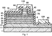
- the schematic sectional view of the semiconductor laser according to the present invention is shown in Fig.1 .
- the n-type nitride semiconductor layer or layers 2 and the p-type nitride semiconductor layer or layers 4 are deposited. Between them there is the active layer 3 of a single quantum well or a multi quantum well structure in the form of a nitride semiconductor containing In. This results in the laser device having a good light emitting efficiency at the wavelength region between near-ultraviolet and green visible light (from 370 nm to 550 nm).
- the n-type nitride semiconductor layer or layers 2 are composed of an n-type GaN contact layer 21, a InGaN crack-preventing layer 22, an n-type AlGaN clad layer 23 and an n-type GaN optical guide layer 24.
- the crack-preventing layer 22 can be omitted.
- the p-type nitride semiconductor layer or layers 4 are composed of an AlGaN protective layer 41, a p-type AlGaN optical guide layer 42, a p-type AlGaN clad layer 43 and a p-type GaN contact layer 44.
- the GaN substrate 1 is comprised with a bulk single crystal and the dislocation thereof is remarkably low, i.e. about 10 4 /cm 2 .
- the n-type contact layer 21 can be formed on the GaN substrate without ELO layer for decreasing dislocation or AlGaN layer for decreasing the pits.
- the resonator of the semiconductor laser device is composed of the active layer 3, the p-type optical guide layer 24, n-type optical guide layer 42 and the cap layer 41.
- the light emitting end face of the resonator is covered with the end face film 5 of single crystal Al x Ga 1-x N (0 ⁇ x ⁇ 1) .
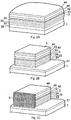
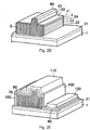
- Fig. 2A-E illustrates a manufacturing method which comprises the steps of forming the laser structure on C-plane of the GaN substrate, covering surface other than the light emitting end face of the resonator with a mask and forming the end face film to cover the light emitting end face.
- Fig. 3A-E illustrates the manufacturing method of the laser device which comprises the steps of forming the laser structure on A-plane of the GaN substrate shown in Fig. 5 , forming the light emitting end face of the resonator on M-plane, forming the light emitting end face by cleavage after formation of ridge and electrode, covering the resonator end face other than the light emitting end face with a mask, and covering the light emitting end face with M-place end face film and then forming laser device in the form of tip by cleavage etc.
- the wafer is prepared on C-plane of GaN substrate 1 by depositing successively the n-type nitride semiconductor layer or layers 2 composed of an n-type contact layer 21, a crack-preventing layer 22, an n-type clad layer 23 and an n-type optical guide layer 24, then the active layer 3 and finally the p-type nitride semiconductor layer or layers 4 composed of a protective layer 41, a p-type optical guide layer 42, a p-type clad layer 43 and a p-type contact layer 44.
- the n-type nitride semiconductor layer or layers 2 composed of an n-type contact layer 21, a crack-preventing layer 22, an n-type clad layer 23 and an n-type optical guide layer 24, then the active layer 3 and finally the p-type nitride semiconductor layer or layers 4 composed of a protective layer 41, a p-type optical guide layer 42, a p-type clad layer 43 and a p-type contact layer 44.
- GaN substrate is used differently from the first method, which results in that n-type nitride semiconductor layer or layers 2 are not formed on the low temperature buffer layer 11 through ELO layer and the dislocation of the epitaxial layer can be decreased.
- the obtained wafer is subject to an etching process, as a result, the end face of the resonator and the n-type contact layer 21 are uncovered and the surface other than the light emitting end face of the resonator is covered by the mask 7( Fig.2B ). Then the end face film 5 is formed on the wafer, whose end faces of the resonator are uncovered, by applying AMMONO method. ( Fig. 2C )
- a ridge is formed by a typical device process after the formation of the end face film and removing the mask 7.
- the ridge stripe which performs the optical wave guide is formed in the direction of the resonator.
- the width of the ridge is from 1.0 ⁇ m to 20 ⁇ m and the ridge reaches the p-type clad layer or the p-type guide layer.
- a buried layer 70 of ZrO 2 film is formed to cover the ridge.
- a p-type ohmic electrode 80 is formed to be in contact with the p-type contact layer 43 which is on the top surface of the ridge. Both of single ridge and plural ridges can be used.
- a multi-stripe-type laser device can be obtained by plural ridges.
- an n-type electrode 90 arranged parallel to the p-type electrode is formed on the surface of the n-type contact layer 21.
- a p-type pad electrode 110 and an n-type pad electrode 120 are formed.
- a SiO 2 / TiO 2 insulating coating is formed to cover the entire device except for the surface of the p-type electrode and the n-type electrode, and due to an alternate arrangement and a patterning of the SiO 2 and TiO 2 layers it serves as the reflecting layer 100 at the moment of laser oscillation.
- each nitride semiconductor laser device is cut out from the wafer by scribing. In this way a finished nitride semiconductor laser device is obtained. ( Fig. 2E , Fig. 1 )
- the protective film can be formed on the end face film to perform an effective resonance. There is a difference of the reflective index between the protective film and the AlGaN end face film.
- the protective film contains at least one element selected from the group consisting of Nb, Ni, Cr, Ti, Cu, Fe, Zr, Hf, W, Rh, Ru, Mg, Al, Sc, Y, Mo, Ta, Co, Pd, Ag, Au, Pt, Ga and the compound such as oxide, nitride and fluoride thereof.
- A-plane of the GaN substrate 1 is cut out from the bulk single crystal as illustrated in Fig. 5 and used as a substrate and a light emitting end face is M-plane so that a laser device can be obtained by cleavage.
- a nitride semiconductor laser device is formed on the GaN substrate 1 similarly as the first method. The same reference numeral is given to the same element to omit the explanation.
- the n-type contact layer 21 is uncovered by etching ( Fig. 3A ). Then a ridge is formed ( Fig.
- the p-type ohmic electrode 80 is formed to be in contact with the p-type contact layer 43 which is on the top surface of the ridge.
- the n-type electrode 90 is formed on the surface of the n-type contact layer 21, and the p-type pad electrode 110 and n-type pad electrode 120 are formed.
- the light emitting end face is formed by cleavage so that the wafer becomes in the form of a bar.
- the end face film 5 is formed in a supercritical ammonia.
- the resultant wafer is subject to cleavage so that a laser device can be obtained.
- Fig. 3E The resultant wafer is subject to cleavage so that a laser device can be obtained.
- the single crystal AlGaN layer can be formed at a low temperature, i.e. from 500°C to 600°C, by applying AMMONO method.
- P-type nitride layer can be formed without degradation of the active layer containing In.
- Fig. 4 illustrates the LED device formed on a GaN substrate 201 obtained by a supercritical ammonia method.
- a modulation doped layer 203 composed of undoped GaN/Si doped GaN/undoped GaN and an active layer 205 composed of InGaN well layer/GaN barrier layer through a superlattice layer 204 are formed.
- LED is obtained by successively depositing a p-type clad layer 206, an undoped AlGaN layer 207 and a p-type contact layer 208 on the top surface of the active layer 205.
- 209 shows a p-type electrode and 210 shows an n-type electrode.
- the bulk single crystal substrate according to the present invention can be used as an intermediate layer instead of the modulation doped layer 203 and the superlattice layer 204, while the n-type contact layer 202 is formed on one bottom side, and the active layer 205, p-type clad layer 206, undoped AlGaN layer 207 and p-type contact layer 208 are successively deposited on top surface so that the similar layer structure can be formed.
- AMMONO method which enables to form the single crystal at a low temperature allows forming an intermediate layer with less crystal dislocation and simplifying the device structure.
- a GaN substrate 1 of 2 inch diameter on C-plane as a growth face is placed in a MOCVD reactor. Temperature is set at 1050°C. Hydrogen is used as a carrier gas, and ammonia and TMG (thrimethylgallium) are used as gaseous materials.
- the formed wafer is subject to annealing in the MOCVD reactor device under the nitrogen atmosphere, at a temperature of 700°C, which additionally reduces resistance of the p-type nitride semiconductor layer or layers.
- the wafer After annealing, the wafer is taken out from the reactor and a protective film (mask) in the form of SiO 2 stripe is deposited on the surface of the top p-type contact layer. Next, by using RIE method, the wafer is etched and stripe is formed, uncovering thereby end faces of the resonator and the surface of the n-type contact layer. The SiO 2 protective film (mask) formed on the surface of the p-type contact layer is removed by using the wet etching method.
- RIE method reactive etching
- the single crystal GaN formed on the surface of the top p-type contact layer is removed by etching.
- the surface of the p-type contact layer is covered with the SiO 2 mask in the form of 1.5 ⁇ m wide strips and etching of the p-type clad layer is continued until ridge is formed on the strip part. Etching is carried out until thickness of the p-type clad layer becomes 0.1 ⁇ m on both sides of ridge.
- a 0.5 ⁇ m thickness ZrO 2 film is formed so that it would cover stripe surfaces over the SiO 2 mask.
- the buried layer 70 in the form of the ZrO 2 film is deposited on the top stripe surface, on the lateral face of ridge and on the surface of the p-type clad layer located on both sides of ridge.
- This ZrO 2 film allows stabilizing a lateral mode at the moment of laser oscillation.
- the p-type electrode 80 in the form of Ni/Au is formed on the p-type contact layer so that an ohmic contact would appear, and the n-type electrode 90 in the form of Ti/Al on the n-type contact layer.
- the wafer is subject to the thermal processing at a temperature of 600°C.
- pad electrode in the form of Ni(1000 ⁇ )-Ti(1000 ⁇ )-Au(8000 ⁇ ) are laid on the p-type and n-type electrode.
- a reflecting film 100 in the form of SiO 2 and TiO 2 is formed, each nitride semiconductor laser device is cut out from the wafer by scribing.
- Each nitride semiconductor laser device manufactured in this way is equipped with a heat sink and the laser oscillation is carried out. Due to an increase of a COD level, prolonged continuous oscillation time is expected - with threshold current density: 2.0 kA/cm 2 , power output: 100 mW, preferably 200 mW, and 405 nm oscillation wavelength.
- a single crystal GaN end face film of 1 ⁇ m thickness is grown on the only one light emitting end face on the stripe part, whereas other stages of production of the nitride semiconductor laser device are carried out similarly as in Example 1.
- Each laser device manufactured in this way is equipped with a heat sink and the laser oscillation is carried out. Prolonged laser lifetime in continuous oscillation mode is expected - with threshold current density: 2.0 kA/ cm 2 , power output: 100 mW and 405 nm oscillation wavelength - similar as in Example 1.
- a SiO 2 protective film in the form of lattice pattern is deposited on the surface of the top p-type contact layer.
- etching of RIE method is carried out so as to uncover an end face of a resonator and the surface of the n-type contact layer.
- the wafer is introduced into the reactor (autoclave) inside which is filled with a supercritical ammonia.
- production of the nitride semiconductor laser device is carried out similarly as in Example 1.
- Each laser device manufactured in this way is equipped with a heat sink and laser oscillation is carried out. Prolonged laser lifetime in continuous oscillation mode is expected - with threshold current density: 2.0 kA/ cm 2 , power output: 100 mW and 405 nm oscillation wavelength - similarly as in Example 1.
- a bulk single crystal substrate by the supercritical ammonia can be used to form nitride semiconductor light emitting devices according to the present invention so that an efficient laser device can be obtained to form a laser device on the substrate having less crystal dislocation causing non-radiative recombination.
- non-polar nitride A-plane or non-polar nitride M-plane can be cut out from the bulk single crystal so that the laser device can be formed on the A-plane or M-plane as an epitaxial growth face.
- the laser device wherein the active layer is not influenced by the polarization and there is no cause of the deterioration of the performance such as the red shift of light emitting, recombination degradation and increase of the threshold current.
- the bulk single crystal layer with less crystal dislocation can be used as an intermediate layer, which enables to simplify the light emitting device structure for the laser device.
- the nitride layer can be formed in the form of single crystal at a low temperature so that the active layer containing In is not influenced by degradation or damaged. Therefore the function and lifetime of the device can be improved.
Landscapes
- Chemical & Material Sciences (AREA)
- Engineering & Computer Science (AREA)
- Crystallography & Structural Chemistry (AREA)
- Physics & Mathematics (AREA)
- Materials Engineering (AREA)
- Metallurgy (AREA)
- Organic Chemistry (AREA)
- Optics & Photonics (AREA)
- Condensed Matter Physics & Semiconductors (AREA)
- General Physics & Mathematics (AREA)
- Electromagnetism (AREA)
- Inorganic Chemistry (AREA)
- Nanotechnology (AREA)
- Life Sciences & Earth Sciences (AREA)
- Biophysics (AREA)
- Semiconductor Lasers (AREA)
- Led Devices (AREA)
- Crystals, And After-Treatments Of Crystals (AREA)
Claims (11)
- Méthode de fabrication d'une structure d'un dispositif émettant de la lumière qui comprend un substrat (1) de nitrure contenant du gallium muni d'une face de croissance épitaxiale ayant une densité de dislocation de 105/cm2 ou moins, et une couche (21) ou des couches (21), (22), (23) et (24) de semi-conducteur de nitrure contenant du gallium de type n, une couche active (3) de semi-conducteur de nitrure contenant du gallium et une couche (44) ou des couches (41), (42), (43) et (44) de semi-conducteur de nitrure contenant du gallium de type p, formées sur ledit substrat par croissance en phase vapeur,
dans laquelle ledit substrat est obtenu à partir d'un monocristal massif de nitrure contenant du gallium préparé par une méthode à l'ammoniaque supercritique, comprenant les étapes suivantes :placer une charge principalement composée de nitrure contenant du gallium ou d'un précurseur de celui-ci dans une zone à plus basse température dans un autoclave pour produire un solvant d'ammoniaque supercritique qui contient au moins de l'ammoniaque et un ion ou des ions d'au moins un métal alcalin, le rapport molaire des ions de métal alcalin sur les autres composants de la solution supercritique étant contrôlé dans une plage allant de 1:200 à 1:2, pour dissoudre le nitrure contenant du gallium, et placer au moins un germe comprenant du GaN ou un germe sélectionné parmi un système cristallin cubique centré sur un corps Mo ou W, un système cristallin hexagonal le plus compact α-Hf ou α-Zr, un diamant à système tétragonal, un système cristallin WC ou W2C à structure WC, un système cristallin SiC à structure ZnO, en particulier α-SiC, TaN, NbN ou AIN, un système hexagonal (P6/mmm) AgB2, AuB2, HfB2 ou ZrB2, et un système hexagonal (P63/mmc) γ-Moc, ε-MbN ou ZrB2 dans une zone à température plus élevée dans l'autoclave où la différence de température entre la zone à température plus élevée et la zone à plus basse température est contrôlée à l'intérieur de la plage de températures de 100 à 800 °C de telle sorte que le nitrure contenant du gallium soit dissous dans la zone à plus basse température et un nitrure contenant du gallium soit recristallisé dans la zone à température plus élevée ;dissoudre la charge dans le solvant d'ammoniaque supercritique dans la zone à plus basse température et générer un flux de convection à partir de la zone à plus basse température vers la zone à température plus élevée pour transporter la charge dissoute ; etrecristalliser la charge dissoute sur le germe dans la zone à température plus élevée à une pression de 1 à 5,5 kbar. - Méthode de fabrication d'une structure d'un dispositif émettant de la lumière selon la revendication 1, dans laquelle ledit substrat est muni d'un plan A ou d'un plan M qui est parallèle à l'axe C de la structure hexagonale pour une croissance épitaxiale, et
dans laquelle ladite couche ou lesdites couches de semi-conducteur de type n sont formées directement ou par le biais d'une couche tampon (11) d'Al(Ga)N sur ledit plan A ou M. - Méthode de fabrication d'une structure d'un dispositif émettant de la lumière selon les revendications 1 ou 2, dans laquelle ledit substrat est un substrat composite (matrice) dans lequel on fait croître un nitrure contenant du gallium sur un substrat hétérogène par la méthode à l'ammoniaque supercritique.
- Méthode de fabrication d'une structure d'un dispositif émettant de la lumière selon la revendication 3, dans laquelle une couche de GaN, d'AIN ou d'AlGaN est préformée sur le substrat hétérogène et ensuite un monocristal massif de nitrure contenant du gallium est formé par-dessus par la méthode à l'ammoniaque supercritique.
- Méthode de fabrication d'une structure d'un dispositif émettant de la lumière selon la revendication 1, dans laquelle une couche non dopée de ladite couche de semi-conducteur de nitrure contenant du gallium de type n est obtenue à partir d'un monocristal massif préparé par la méthode à l'ammoniaque supercritique, dans laquelle au moins une couche de semi-conducteur de nitrure de type n ou des couches contenant des impuretés de type n sont formées sur une face de ladite face de croissance épitaxiale, et
dans laquelle ladite couche active de nitrure et ladite couche ou les couches de semi-conducteur de nitrure de type p sont formées directement ou par le biais d'une couche ou des couches de semi-conducteur de nitrure de type n sur l'autre face de ladite face de croissance épitaxiale. - Méthode de fabrication d'une structure d'un dispositif émettant de la lumière selon la revendication 5, dans laquelle ledit substrat de monocristal massif est muni d'un plan A ou d'un plan M qui est parallèle à l'axe C de la structure hexagonale pour une croissance épitaxiale.
- Méthode de fabrication d'une structure d'un dispositif émettant de la lumière selon la revendication 1, dans laquelle la couche active de semi-conducteur de nitrure contenant du gallium contient de l'In, et dans laquelle un film protecteur (41) de monocristal AlxGa1-xN (0≤x≤1) est formé sur ladite couche active de nitrure par la méthode à l'ammoniaque supercritique.
- Méthode de fabrication d'une structure d'un dispositif émettant de la lumière selon la revendication 7, dans laquelle ladite couche active comprend une structure à puits quantique comprenant au moins une couche à puits InGaN ou une couche à puits InAlGaN.
- Méthode de fabrication d'une structure d'un dispositif émettant de la lumière selon les revendications 7 ou 8, dans laquelle ledit dispositif émettant de la lumière est formé sur le plan A ou le plan M d'un substrat de GaN.
- Méthode de fabrication d'une structure d'un dispositif émettant de la lumière selon l'une quelconque des revendications 1, 2 ou 7, dans laquelle ledit dispositif émettant de la lumière est un dispositif à laser semi-conducteur et est formé sur un plan A d'un substrat de GaN monocristallin massif et la face émettant de la lumière d'un résonateur du dispositif à laser semi-conducteur est le plan M, sur lequel un film à face terminale est formé.
- Méthode de fabrication d'une structure d'un dispositif émettant de la lumière selon l'une quelconque des revendications 1 à 10, dans laquelle la zone à température plus élevée est située en dessous de la zone à plus basse température.
Applications Claiming Priority (5)
| Application Number | Priority Date | Filing Date | Title |
|---|---|---|---|
| PL35037501 | 2001-10-26 | ||
| PL35037501A PL350375A1 (en) | 2001-10-26 | 2001-10-26 | Epitaxial layer substrate |
| PL35473902 | 2002-06-26 | ||
| PL02354739A PL354739A1 (en) | 2002-06-26 | 2002-06-26 | Nitride semiconductor laser |
| PCT/IB2002/004441 WO2003043150A1 (fr) | 2001-10-26 | 2002-10-28 | Structure d'element electoluminescent a couche monocristalline non epitaxiee de nitrure |
Publications (4)
| Publication Number | Publication Date |
|---|---|
| EP1453159A1 EP1453159A1 (fr) | 2004-09-01 |
| EP1453159A4 EP1453159A4 (fr) | 2007-10-03 |
| EP1453159B1 true EP1453159B1 (fr) | 2017-09-06 |
| EP1453159B8 EP1453159B8 (fr) | 2017-12-13 |
Family
ID=26653408
Family Applications (2)
| Application Number | Title | Priority Date | Filing Date |
|---|---|---|---|
| EP02775396A Withdrawn EP1453158A4 (fr) | 2001-10-26 | 2002-10-28 | Laser a semi-conducteurs a base de nitrure et procede de production de ce laser |
| EP02803072.4A Expired - Lifetime EP1453159B8 (fr) | 2001-10-26 | 2002-10-28 | Structure d'un dispositif emettant de la lumiere a couche monocristalline non epitaxiee de nitrure |
Family Applications Before (1)
| Application Number | Title | Priority Date | Filing Date |
|---|---|---|---|
| EP02775396A Withdrawn EP1453158A4 (fr) | 2001-10-26 | 2002-10-28 | Laser a semi-conducteurs a base de nitrure et procede de production de ce laser |
Country Status (8)
| Country | Link |
|---|---|
| US (3) | US7057211B2 (fr) |
| EP (2) | EP1453158A4 (fr) |
| JP (2) | JP4383172B2 (fr) |
| KR (2) | KR100679377B1 (fr) |
| CN (2) | CN1263206C (fr) |
| PL (2) | PL374180A1 (fr) |
| TW (1) | TWI263387B (fr) |
| WO (2) | WO2003036771A1 (fr) |
Families Citing this family (154)
| Publication number | Priority date | Publication date | Assignee | Title |
|---|---|---|---|---|
| US6596079B1 (en) | 2000-03-13 | 2003-07-22 | Advanced Technology Materials, Inc. | III-V nitride substrate boule and method of making and using the same |
| IL159165A0 (en) | 2001-06-06 | 2004-06-01 | Ammono Sp Zoo | Process and apparatus for obtaining bulk monocrystalline gallium containing nitride |
| EP1453158A4 (fr) | 2001-10-26 | 2007-09-19 | Ammono Sp Zoo | Laser a semi-conducteurs a base de nitrure et procede de production de ce laser |
| PL225235B1 (pl) * | 2001-10-26 | 2017-03-31 | Ammono Spółka Z Ograniczoną Odpowiedzialnością | Objętościowy monokryształ azotkowy oraz jego zastosowanie jako podłoże do epitaksji |
| US8545629B2 (en) | 2001-12-24 | 2013-10-01 | Crystal Is, Inc. | Method and apparatus for producing large, single-crystals of aluminum nitride |
| WO2003089695A1 (fr) * | 2002-04-15 | 2003-10-30 | The Regents Of The University Of California | Films minces de nitrure de gallium a plan a non polaire obtenus par depot chimique en phase vapeur metalorganique |
| US8809867B2 (en) * | 2002-04-15 | 2014-08-19 | The Regents Of The University Of California | Dislocation reduction in non-polar III-nitride thin films |
| US20060138431A1 (en) | 2002-05-17 | 2006-06-29 | Robert Dwilinski | Light emitting device structure having nitride bulk single crystal layer |
| AU2002354467A1 (en) * | 2002-05-17 | 2003-12-02 | Ammono Sp.Zo.O. | Light emitting element structure having nitride bulk single crystal layer |
| AU2003285769A1 (en) | 2002-12-11 | 2004-06-30 | Ammono Sp. Z O.O. | A substrate for epitaxy and a method of preparing the same |
| US7811380B2 (en) | 2002-12-11 | 2010-10-12 | Ammono Sp. Z O.O. | Process for obtaining bulk mono-crystalline gallium-containing nitride |
| EP1576671A4 (fr) * | 2002-12-16 | 2006-10-25 | Univ California | Croissance de nitrure de gallium a plan a non polaires et a geometrie planaire par epitaxie en phase vapeur de l'hydrure |
| US7186302B2 (en) * | 2002-12-16 | 2007-03-06 | The Regents Of The University Of California | Fabrication of nonpolar indium gallium nitride thin films, heterostructures and devices by metalorganic chemical vapor deposition |
| US7427555B2 (en) * | 2002-12-16 | 2008-09-23 | The Regents Of The University Of California | Growth of planar, non-polar gallium nitride by hydride vapor phase epitaxy |
| EP1697965A4 (fr) * | 2003-04-15 | 2011-02-09 | Univ California | Puits quantiques (a1, b, in, ga)n non polaires |
| KR101034055B1 (ko) | 2003-07-18 | 2011-05-12 | 엘지이노텍 주식회사 | 발광 다이오드 및 그 제조방법 |
| JP3841092B2 (ja) * | 2003-08-26 | 2006-11-01 | 住友電気工業株式会社 | 発光装置 |
| US7323256B2 (en) * | 2003-11-13 | 2008-01-29 | Cree, Inc. | Large area, uniformly low dislocation density GaN substrate and process for making the same |
| US7118813B2 (en) * | 2003-11-14 | 2006-10-10 | Cree, Inc. | Vicinal gallium nitride substrate for high quality homoepitaxy |
| JP2005191530A (ja) * | 2003-12-03 | 2005-07-14 | Sumitomo Electric Ind Ltd | 発光装置 |
| KR100576856B1 (ko) * | 2003-12-23 | 2006-05-10 | 삼성전기주식회사 | 질화물 반도체 발광소자 및 제조방법 |
| ATE418806T1 (de) * | 2004-04-02 | 2009-01-15 | Nichia Corp | Nitrid-halbleiterlaservorrichtung |
| JP2005340765A (ja) * | 2004-04-30 | 2005-12-08 | Sumitomo Electric Ind Ltd | 半導体発光素子 |
| US7504274B2 (en) * | 2004-05-10 | 2009-03-17 | The Regents Of The University Of California | Fabrication of nonpolar indium gallium nitride thin films, heterostructures and devices by metalorganic chemical vapor deposition |
| EP1787330A4 (fr) * | 2004-05-10 | 2011-04-13 | Univ California | Fabrication de films ultra-minces de nitrure d'indium et de gallium, d'heterostructures et d'autres pieces par deposition en phase vapeur d'organometallique |
| US7956360B2 (en) * | 2004-06-03 | 2011-06-07 | The Regents Of The University Of California | Growth of planar reduced dislocation density M-plane gallium nitride by hydride vapor phase epitaxy |
| US20080163814A1 (en) * | 2006-12-12 | 2008-07-10 | The Regents Of The University Of California | CRYSTAL GROWTH OF M-PLANE AND SEMIPOLAR PLANES OF (Al, In, Ga, B)N ON VARIOUS SUBSTRATES |
| US7575947B2 (en) | 2005-09-09 | 2009-08-18 | The Regents Of The University Of California | Method for enhancing growth of semi-polar (Al,In,Ga,B)N via metalorganic chemical vapor deposition |
| KR100848379B1 (ko) * | 2004-06-11 | 2008-07-25 | 암모노 에스피. 제트오. 오. | Ⅹⅲ족 원소 질화물의 층으로 이루어진 고 전자이동도트랜지스터 및 그 제조 방법 |
| PL1769105T3 (pl) | 2004-06-11 | 2014-11-28 | Ammono S A | Objętościowy monokrystaliczny azotek galu oraz sposób jego wytwarzania |
| PL1652586T5 (pl) * | 2004-10-26 | 2016-08-31 | Smidth As F L | System wytwarzający impulsy dla odpylacza elektrostatycznego |
| PL371405A1 (pl) | 2004-11-26 | 2006-05-29 | Ammono Sp.Z O.O. | Sposób wytwarzania objętościowych monokryształów metodą wzrostu na zarodku |
| JP4451371B2 (ja) * | 2004-12-20 | 2010-04-14 | シャープ株式会社 | 窒化物半導体レーザ素子 |
| CN1805230B (zh) * | 2004-12-20 | 2011-06-01 | 夏普株式会社 | 氮化物半导体发光元件及其制造方法 |
| CN100352116C (zh) * | 2005-01-18 | 2007-11-28 | 北京大学 | 自然解理腔面的GaN基激光二极管的制备方法 |
| EP2315253A1 (fr) | 2005-03-10 | 2011-04-27 | The Regents of the University of California | Procédé de croissance épitaxiale d'un nitrure de gallium semi-polaire ayant une surface plane et produit relatif |
| PL1701203T3 (pl) * | 2005-03-10 | 2007-10-31 | Nanogate Advanced Mat Gmbh | Płaski ekran |
| TW200703463A (en) * | 2005-05-31 | 2007-01-16 | Univ California | Defect reduction of non-polar and semi-polar III-nitrides with sidewall lateral epitaxial overgrowth (SLEO) |
| TWI377602B (en) * | 2005-05-31 | 2012-11-21 | Japan Science & Tech Agency | Growth of planar non-polar {1-100} m-plane gallium nitride with metalorganic chemical vapor deposition (mocvd) |
| KR101351396B1 (ko) | 2005-06-01 | 2014-02-07 | 재팬 사이언스 앤드 테크놀로지 에이젼시 | 반극성 (Ga,Al,In,B)N 박막들, 헤테로구조들, 및소자들의 성장 및 제조에 대한 기술 |
| WO2007008394A1 (fr) | 2005-07-11 | 2007-01-18 | Cree, Inc. | Orientation d'une diode laser sur un substrat desoriente |
| JP5285835B2 (ja) * | 2005-07-13 | 2013-09-11 | 株式会社東芝 | 半導体素子およびその製造方法 |
| KR100706952B1 (ko) * | 2005-07-22 | 2007-04-12 | 삼성전기주식회사 | 수직 구조 질화갈륨계 발광다이오드 소자 및 그 제조방법 |
| JP2007081075A (ja) * | 2005-09-14 | 2007-03-29 | Sharp Corp | 窒化物半導体レーザ素子およびその製造方法 |
| US7635874B2 (en) * | 2005-09-26 | 2009-12-22 | Avago Technologies Ecbu Ip (Singapore) Pte. Ltd. | Edge-emitting LED assembly |
| JP2007103814A (ja) * | 2005-10-07 | 2007-04-19 | Sharp Corp | 窒化物半導体発光素子およびその製造方法 |
| US7641735B2 (en) | 2005-12-02 | 2010-01-05 | Crystal Is, Inc. | Doped aluminum nitride crystals and methods of making them |
| JP4535997B2 (ja) * | 2005-12-09 | 2010-09-01 | シャープ株式会社 | 窒化物半導体レーザ素子およびその製造方法 |
| JP5191650B2 (ja) * | 2005-12-16 | 2013-05-08 | シャープ株式会社 | 窒化物半導体発光素子および窒化物半導体発光素子の製造方法 |
| KR100853241B1 (ko) * | 2005-12-16 | 2008-08-20 | 샤프 가부시키가이샤 | 질화물 반도체 발광소자 및 질화물 반도체 레이저 소자의제조방법 |
| WO2007084782A2 (fr) | 2006-01-20 | 2007-07-26 | The Regents Of The University Of California | Procédé amélioré d'étirement de (al, in, ga, b)n semipolaire |
| JP2007266574A (ja) * | 2006-02-28 | 2007-10-11 | Sanyo Electric Co Ltd | 半導体レーザ素子及び半導体レーザ素子の製造方法 |
| CN100568563C (zh) * | 2006-03-06 | 2009-12-09 | 夏普株式会社 | 氮化物半导体器件及其制备方法 |
| JP5004597B2 (ja) * | 2006-03-06 | 2012-08-22 | シャープ株式会社 | 窒化物半導体発光素子および窒化物半導体発光素子の製造方法 |
| JP5430826B2 (ja) | 2006-03-08 | 2014-03-05 | シャープ株式会社 | 窒化物半導体レーザ素子 |
| JP4694395B2 (ja) * | 2006-03-22 | 2011-06-08 | 日本オプネクスト株式会社 | 窒化物半導体発光素子及びその製造方法 |
| JP4929776B2 (ja) * | 2006-03-22 | 2012-05-09 | 日亜化学工業株式会社 | 窒化物半導体レーザ素子 |
| US9034103B2 (en) | 2006-03-30 | 2015-05-19 | Crystal Is, Inc. | Aluminum nitride bulk crystals having high transparency to ultraviolet light and methods of forming them |
| JP4444304B2 (ja) * | 2006-04-24 | 2010-03-31 | シャープ株式会社 | 窒化物半導体発光素子および窒化物半導体発光素子の製造方法 |
| US7488384B2 (en) * | 2006-05-03 | 2009-02-10 | Ohio University | Direct pyrolysis route to GaN quantum dots |
| JP5250856B2 (ja) * | 2006-06-13 | 2013-07-31 | 豊田合成株式会社 | 窒化ガリウム系化合物半導体発光素子の製造方法 |
| JP5008911B2 (ja) * | 2006-07-04 | 2012-08-22 | ローム株式会社 | 半導体発光素子およびその製造方法 |
| GB2439973A (en) * | 2006-07-13 | 2008-01-16 | Sharp Kk | Modifying the optical properties of a nitride optoelectronic device |
| US20080025037A1 (en) * | 2006-07-28 | 2008-01-31 | Visteon Global Technologies, Inc. | LED headlamp |
| JP2008109066A (ja) * | 2006-09-29 | 2008-05-08 | Rohm Co Ltd | 発光素子 |
| EP2100990A1 (fr) * | 2006-10-16 | 2009-09-16 | Mitsubishi Chemical Corporation | Procédé de fabrication d'un semiconducteur à base de nitrure, agent d'augmentation de la vitesse de croissance cristalline, monocristal de nitrure, tranche et dispositif |
| US8193020B2 (en) | 2006-11-15 | 2012-06-05 | The Regents Of The University Of California | Method for heteroepitaxial growth of high-quality N-face GaN, InN, and AlN and their alloys by metal organic chemical vapor deposition |
| JP2010509177A (ja) * | 2006-11-15 | 2010-03-25 | ザ リージェンツ オブ ザ ユニバーシティ オブ カリフォルニア | 有機金属化学気相成長法による、高品質のN面GaN、InNおよびAlNならびにそれらの合金のヘテロエピタキシャル成長の方法 |
| JP5042609B2 (ja) * | 2006-12-08 | 2012-10-03 | シャープ株式会社 | 窒化物系半導体素子 |
| TWI533351B (zh) * | 2006-12-11 | 2016-05-11 | 美國加利福尼亞大學董事會 | 高效能非極性第三族氮化物光學裝置之金屬有機化學氣相沈積生長 |
| US7646798B2 (en) | 2006-12-28 | 2010-01-12 | Nichia Corporation | Nitride semiconductor laser element |
| KR100920915B1 (ko) * | 2006-12-28 | 2009-10-12 | 서울옵토디바이스주식회사 | 초격자 구조의 장벽층을 갖는 발광 다이오드 |
| JP4978454B2 (ja) * | 2006-12-28 | 2012-07-18 | 日亜化学工業株式会社 | 窒化物半導体レーザ素子 |
| WO2008088838A1 (fr) | 2007-01-17 | 2008-07-24 | Crystal Is, Inc. | Réduction des défauts de croissance de cristaux de nitrure d'aluminium ensemencés |
| US9771666B2 (en) | 2007-01-17 | 2017-09-26 | Crystal Is, Inc. | Defect reduction in seeded aluminum nitride crystal growth |
| US8080833B2 (en) | 2007-01-26 | 2011-12-20 | Crystal Is, Inc. | Thick pseudomorphic nitride epitaxial layers |
| US7668218B2 (en) * | 2007-02-20 | 2010-02-23 | Nichia Corporation | Nitride semiconductor laser element |
| US7764722B2 (en) * | 2007-02-26 | 2010-07-27 | Nichia Corporation | Nitride semiconductor laser element |
| EP1976031A3 (fr) * | 2007-03-29 | 2010-09-08 | Seoul Opto Device Co., Ltd. | Diode électroluminescente disposant de couches de barrière et/ou forage avec une structure de réseau superposé |
| US7843980B2 (en) * | 2007-05-16 | 2010-11-30 | Rohm Co., Ltd. | Semiconductor laser diode |
| KR101488545B1 (ko) | 2007-05-17 | 2015-02-02 | 미쓰비시 가가꾸 가부시키가이샤 | Iii 족 질화물 반도체 결정의 제조 방법, iii 족 질화물 반도체 기판 및 반도체 발광 디바이스 |
| JP2008300540A (ja) * | 2007-05-30 | 2008-12-11 | Sumitomo Electric Ind Ltd | 半導体発光素子の製造方法 |
| JP4310352B2 (ja) * | 2007-06-05 | 2009-08-05 | シャープ株式会社 | 発光デバイスおよび発光デバイスの製造方法 |
| JP5118392B2 (ja) * | 2007-06-08 | 2013-01-16 | ローム株式会社 | 半導体発光素子およびその製造方法 |
| KR100872717B1 (ko) * | 2007-06-22 | 2008-12-05 | 엘지이노텍 주식회사 | 발광 소자 및 그 제조방법 |
| US7701995B2 (en) | 2007-07-06 | 2010-04-20 | Nichia Corporation | Nitride semiconductor laser element |
| JP4979011B2 (ja) * | 2007-07-20 | 2012-07-18 | シャープ株式会社 | 窒化物半導体レーザ素子およびその製造方法 |
| KR100877774B1 (ko) * | 2007-09-10 | 2009-01-16 | 서울옵토디바이스주식회사 | 개선된 구조의 발광다이오드 |
| CN101836304B (zh) * | 2007-10-25 | 2015-04-29 | 皇家飞利浦电子股份有限公司 | 偏振发光器件 |
| JP5014967B2 (ja) * | 2007-12-06 | 2012-08-29 | シャープ株式会社 | 発光素子及び発光素子の製造方法 |
| KR100998008B1 (ko) | 2007-12-17 | 2010-12-03 | 삼성엘이디 주식회사 | 소자 형성용 기판의 제조방법 및 질화물계 반도체 레이저다이오드의 제조방법 |
| JP5053893B2 (ja) * | 2008-03-07 | 2012-10-24 | 住友電気工業株式会社 | 窒化物半導体レーザを作製する方法 |
| JP2009253047A (ja) * | 2008-04-07 | 2009-10-29 | Sumitomo Electric Ind Ltd | Iii族窒化物発光素子及びエピタキシャルウエハ |
| US8673074B2 (en) * | 2008-07-16 | 2014-03-18 | Ostendo Technologies, Inc. | Growth of planar non-polar {1 -1 0 0} M-plane and semi-polar {1 1 -2 2} gallium nitride with hydride vapor phase epitaxy (HVPE) |
| WO2010051537A1 (fr) | 2008-10-31 | 2010-05-06 | The Regents Of The University Of California | Dispositif optoélectronique à base d'alliages de nitrure d'aluminium-indium et de nitrure d'aluminium-indium-gallium non polaires et semi-polaires |
| JP2010135516A (ja) * | 2008-12-03 | 2010-06-17 | Panasonic Corp | 窒化物半導体発光装置 |
| KR100999695B1 (ko) * | 2009-02-16 | 2010-12-08 | 엘지이노텍 주식회사 | 반도체 발광소자 및 그 제조방법 |
| US8247886B1 (en) | 2009-03-09 | 2012-08-21 | Soraa, Inc. | Polarization direction of optical devices using selected spatial configurations |
| US8299473B1 (en) | 2009-04-07 | 2012-10-30 | Soraa, Inc. | Polarized white light devices using non-polar or semipolar gallium containing materials and transparent phosphors |
| JP5383313B2 (ja) * | 2009-05-20 | 2014-01-08 | パナソニック株式会社 | 窒化物半導体発光装置 |
| US8791499B1 (en) | 2009-05-27 | 2014-07-29 | Soraa, Inc. | GaN containing optical devices and method with ESD stability |
| TWI478381B (zh) * | 2009-06-08 | 2015-03-21 | Epistar Corp | 發光元件及其製造方法 |
| EP2267197A1 (fr) * | 2009-06-25 | 2010-12-29 | AMMONO Sp.z o.o. | Procédé d'obtention de nitrures monocristallins en vrac contenant du gallium, nitrures monocristallins en vrac contenant du gallium, substances fabriquées à partir de ces nitrures et dispositifs fabriqués sur de tels substrats. |
| US9000466B1 (en) | 2010-08-23 | 2015-04-07 | Soraa, Inc. | Methods and devices for light extraction from a group III-nitride volumetric LED using surface and sidewall roughening |
| US8933644B2 (en) | 2009-09-18 | 2015-01-13 | Soraa, Inc. | LED lamps with improved quality of light |
| US9293644B2 (en) * | 2009-09-18 | 2016-03-22 | Soraa, Inc. | Power light emitting diode and method with uniform current density operation |
| CN107256915A (zh) * | 2009-09-18 | 2017-10-17 | 天空公司 | 发光二极管器件 |
| US9583678B2 (en) | 2009-09-18 | 2017-02-28 | Soraa, Inc. | High-performance LED fabrication |
| US8629065B2 (en) * | 2009-11-06 | 2014-01-14 | Ostendo Technologies, Inc. | Growth of planar non-polar {10-10} M-plane gallium nitride with hydride vapor phase epitaxy (HVPE) |
| US8399948B2 (en) | 2009-12-04 | 2013-03-19 | Lg Innotek Co., Ltd. | Light emitting device, light emitting device package and lighting system |
| US8740413B1 (en) | 2010-02-03 | 2014-06-03 | Soraa, Inc. | System and method for providing color light sources in proximity to predetermined wavelength conversion structures |
| US8905588B2 (en) | 2010-02-03 | 2014-12-09 | Sorra, Inc. | System and method for providing color light sources in proximity to predetermined wavelength conversion structures |
| US10147850B1 (en) | 2010-02-03 | 2018-12-04 | Soraa, Inc. | System and method for providing color light sources in proximity to predetermined wavelength conversion structures |
| US9450143B2 (en) * | 2010-06-18 | 2016-09-20 | Soraa, Inc. | Gallium and nitrogen containing triangular or diamond-shaped configuration for optical devices |
| JP5806734B2 (ja) | 2010-06-30 | 2015-11-10 | クリスタル アイエス, インコーポレーテッドCrystal Is, Inc. | 熱勾配制御による窒化アルミニウム大単結晶成長 |
| KR200458355Y1 (ko) * | 2010-07-16 | 2012-02-15 | 안수철 | 변신만화액자 |
| JP5113305B2 (ja) * | 2011-01-21 | 2013-01-09 | パナソニック株式会社 | 窒化ガリウム系化合物半導体発光素子および当該発光素子を備える光源 |
| US8786053B2 (en) | 2011-01-24 | 2014-07-22 | Soraa, Inc. | Gallium-nitride-on-handle substrate materials and devices and method of manufacture |
| JP5069386B1 (ja) * | 2011-04-06 | 2012-11-07 | パナソニック株式会社 | 半導体発光デバイス |
| US8962359B2 (en) | 2011-07-19 | 2015-02-24 | Crystal Is, Inc. | Photon extraction from nitride ultraviolet light-emitting devices |
| US8686431B2 (en) | 2011-08-22 | 2014-04-01 | Soraa, Inc. | Gallium and nitrogen containing trilateral configuration for optical devices |
| US8912025B2 (en) | 2011-11-23 | 2014-12-16 | Soraa, Inc. | Method for manufacture of bright GaN LEDs using a selective removal process |
| JP5431441B2 (ja) * | 2011-11-30 | 2014-03-05 | シャープ株式会社 | 窒化物半導体発光素子 |
| EP2823515A4 (fr) | 2012-03-06 | 2015-08-19 | Soraa Inc | Diodes électroluminescentes à couches de matériau à faible indice de réfraction destinées à réduire des effets de guidage de lumière |
| US10559939B1 (en) * | 2012-04-05 | 2020-02-11 | Soraa Laser Diode, Inc. | Facet on a gallium and nitrogen containing laser diode |
| US9800016B1 (en) | 2012-04-05 | 2017-10-24 | Soraa Laser Diode, Inc. | Facet on a gallium and nitrogen containing laser diode |
| US8971368B1 (en) | 2012-08-16 | 2015-03-03 | Soraa Laser Diode, Inc. | Laser devices having a gallium and nitrogen containing semipolar surface orientation |
| US9978904B2 (en) | 2012-10-16 | 2018-05-22 | Soraa, Inc. | Indium gallium nitride light emitting devices |
| US8802471B1 (en) | 2012-12-21 | 2014-08-12 | Soraa, Inc. | Contacts for an n-type gallium and nitrogen substrate for optical devices |
| US9761763B2 (en) | 2012-12-21 | 2017-09-12 | Soraa, Inc. | Dense-luminescent-materials-coated violet LEDs |
| EP2973664B1 (fr) | 2013-03-15 | 2020-10-14 | Crystal Is, Inc. | Dispositif émetteur d'ultraviolet et procédé pour former un contact sur un dispositif émetteur d'ultraviolet |
| US8994033B2 (en) | 2013-07-09 | 2015-03-31 | Soraa, Inc. | Contacts for an n-type gallium and nitrogen substrate for optical devices |
| WO2015025931A1 (fr) | 2013-08-22 | 2015-02-26 | 日本碍子株式会社 | Procédé de production de nitrure d'un élément du groupe 13, et composition à l'état de masse fondue |
| US9410664B2 (en) | 2013-08-29 | 2016-08-09 | Soraa, Inc. | Circadian friendly LED light source |
| CN105102695B (zh) | 2013-12-18 | 2018-06-12 | 日本碍子株式会社 | 复合基板和功能元件 |
| US9246311B1 (en) | 2014-11-06 | 2016-01-26 | Soraa Laser Diode, Inc. | Method of manufacture for an ultraviolet laser diode |
| TWI560905B (en) * | 2014-11-19 | 2016-12-01 | Univ Nat Sun Yat Sen | A light emitting element and manufacturing method thereof |
| US10381508B2 (en) | 2014-11-19 | 2019-08-13 | National Sun Yat-Sen University | Light emitting element with an enhanced electroluminescence effect |
| US10505072B2 (en) * | 2016-12-16 | 2019-12-10 | Nichia Corporation | Method for manufacturing light emitting element |
| JP6931827B2 (ja) | 2017-04-07 | 2021-09-08 | 日本製鋼所M&E株式会社 | 結晶製造用圧力容器 |
| JP6870500B2 (ja) * | 2017-06-27 | 2021-05-12 | 住友電気工業株式会社 | 量子カスケード半導体レーザ |
| JP6939120B2 (ja) | 2017-06-19 | 2021-09-22 | 住友電気工業株式会社 | 量子カスケード半導体レーザ、発光装置、半導体レーザを作製する方法 |
| JP6911567B2 (ja) | 2017-06-22 | 2021-07-28 | 住友電気工業株式会社 | 量子カスケード半導体レーザ |
| JP6939119B2 (ja) | 2017-06-19 | 2021-09-22 | 住友電気工業株式会社 | 量子カスケード半導体レーザ、発光装置、半導体レーザを作製する方法 |
| US10404038B2 (en) * | 2017-06-22 | 2019-09-03 | Sumitomo Electric Industries, Ltd. | Quantum cascade laser |
| US10476235B2 (en) | 2017-06-22 | 2019-11-12 | Sumitomo Electric Industries, Ltd. | Quantum cascade laser |
| US10476237B2 (en) | 2017-06-22 | 2019-11-12 | Sumitomo Electric Industries, Ltd. | Quantum cascade laser |
| JP7246038B2 (ja) * | 2018-09-14 | 2023-03-27 | 旭化成株式会社 | 窒化物半導体レーザダイオード |
| FR3105586B1 (fr) * | 2019-12-23 | 2023-07-21 | Commissariat Energie Atomique | Procédé de fabrication d’une diode électroluminescente comportant une étape de dimensionnement d’une couche semiconductrice |
| US11909172B2 (en) * | 2020-01-08 | 2024-02-20 | Asahi Kasei Kabushiki Kaisha | Method for manufacturing optical device and optical device |
| CN115298918A (zh) * | 2020-03-19 | 2022-11-04 | 松下控股株式会社 | 半导体激光元件 |
| US20210313760A1 (en) * | 2020-04-06 | 2021-10-07 | Asahi Kasei Kabushiki Kaisha | Method for manufacturing semiconductor laser diode and semiconductor laser diode |
| US12191626B1 (en) | 2020-07-31 | 2025-01-07 | Kyocera Sld Laser, Inc. | Vertically emitting laser devices and chip-scale-package laser devices and laser-based, white light emitting devices |
| CN113437187B (zh) * | 2021-08-26 | 2022-01-25 | 北京大学深圳研究生院 | 一种发光二极管超临界处理方法 |
Family Cites Families (148)
| Publication number | Priority date | Publication date | Assignee | Title |
|---|---|---|---|---|
| JPH0722692B2 (ja) | 1988-08-05 | 1995-03-15 | 株式会社日本製鋼所 | 水熱合成用容器 |
| JPH02137287A (ja) | 1988-11-17 | 1990-05-25 | Sanyo Electric Co Ltd | 半導体レーザ装置 |
| CN1014535B (zh) | 1988-12-30 | 1991-10-30 | 中国科学院物理研究所 | 利用改进的矿化剂生长磷酸钛氧钾单晶的方法 |
| US5096860A (en) | 1990-05-25 | 1992-03-17 | Alcan International Limited | Process for producing unagglomerated single crystals of aluminum nitride |
| KR920004181B1 (ko) | 1990-09-13 | 1992-05-30 | 한국과학기술연구원 | 입방정질화붕소의 제조방법 |
| US5190738A (en) | 1991-06-17 | 1993-03-02 | Alcan International Limited | Process for producing unagglomerated single crystals of aluminum nitride |
| US5156581A (en) | 1991-06-21 | 1992-10-20 | Chow John W | Finger conditioning device |
| US5306662A (en) | 1991-11-08 | 1994-04-26 | Nichia Chemical Industries, Ltd. | Method of manufacturing P-type compound semiconductor |
| US5456201A (en) * | 1992-01-16 | 1995-10-10 | Bobst; Glen L. | Air bubble lubricated boat hull |
| CN1065289A (zh) | 1992-04-28 | 1992-10-14 | 抚顺石油学院 | 洁厕灵 |
| CN1036414C (zh) | 1992-11-03 | 1997-11-12 | 程大酉 | 改进的回热并联复合双流体燃气轮机装置及其操作方法 |
| US5456204A (en) | 1993-05-28 | 1995-10-10 | Alfa Quartz, C.A. | Filtering flow guide for hydrothermal crystal growth |
| JP3184717B2 (ja) | 1993-10-08 | 2001-07-09 | 三菱電線工業株式会社 | GaN単結晶およびその製造方法 |
| US5679152A (en) * | 1994-01-27 | 1997-10-21 | Advanced Technology Materials, Inc. | Method of making a single crystals Ga*N article |
| JPH07249830A (ja) * | 1994-03-10 | 1995-09-26 | Hitachi Ltd | 半導体発光素子の製造方法 |
| WO1995027815A1 (fr) * | 1994-04-08 | 1995-10-19 | Japan Energy Corporation | Procede de tirage d'un cristal semi-conducteur constitue par un compose de nitrure de gallium et dispositif semi-conducteur a composes de nitrure de gallium |
| US5599520A (en) | 1994-11-03 | 1997-02-04 | Garces; Juan M. | Synthesis of crystalline porous solids in ammonia |
| US5777350A (en) | 1994-12-02 | 1998-07-07 | Nichia Chemical Industries, Ltd. | Nitride semiconductor light-emitting device |
| JPH08250802A (ja) * | 1995-03-09 | 1996-09-27 | Fujitsu Ltd | 半導体レーザ及びその製造方法 |
| US5679965A (en) | 1995-03-29 | 1997-10-21 | North Carolina State University | Integrated heterostructures of Group III-V nitride semiconductor materials including epitaxial ohmic contact, non-nitride buffer layer and methods of fabricating same |
| US5670798A (en) * | 1995-03-29 | 1997-09-23 | North Carolina State University | Integrated heterostructures of Group III-V nitride semiconductor materials including epitaxial ohmic contact non-nitride buffer layer and methods of fabricating same |
| JP3728332B2 (ja) * | 1995-04-24 | 2005-12-21 | シャープ株式会社 | 化合物半導体発光素子 |
| GB2310083B (en) | 1995-08-31 | 1999-07-28 | Toshiba Kk | Blue light emitting element and method of manufacturing same |
| DE69622277T2 (de) * | 1995-09-18 | 2003-03-27 | Hitachi, Ltd. | Halbleitermaterial, verfahren zur herstellung des halbleitermaterials und eine halbleitervorrichtung |
| JPH09134878A (ja) * | 1995-11-10 | 1997-05-20 | Matsushita Electron Corp | 窒化ガリウム系化合物半導体の製造方法 |
| US5981980A (en) | 1996-04-22 | 1999-11-09 | Sony Corporation | Semiconductor laminating structure |
| JPH107496A (ja) | 1996-06-25 | 1998-01-13 | Hitachi Cable Ltd | 窒化物結晶の製造方法およびその装置 |
| CN1065289C (zh) | 1996-07-22 | 2001-05-02 | 中国科学院物理研究所 | 一种制备掺杂钒酸盐单晶的水热生长方法 |
| JP3179346B2 (ja) * | 1996-08-27 | 2001-06-25 | 松下電子工業株式会社 | 窒化ガリウム結晶の製造方法 |
| JPH1084161A (ja) * | 1996-09-06 | 1998-03-31 | Sumitomo Electric Ind Ltd | 半導体レーザ及びその製造方法 |
| JP4018177B2 (ja) * | 1996-09-06 | 2007-12-05 | 株式会社東芝 | 窒化ガリウム系化合物半導体発光素子 |
| US6031858A (en) * | 1996-09-09 | 2000-02-29 | Kabushiki Kaisha Toshiba | Semiconductor laser and method of fabricating same |
| WO1998019375A1 (fr) * | 1996-10-30 | 1998-05-07 | Hitachi, Ltd. | Machine de traitement optique de l'information et dispositif a semi-conducteur emetteur de lumiere afferent |
| US6177292B1 (en) | 1996-12-05 | 2001-01-23 | Lg Electronics Inc. | Method for forming GaN semiconductor single crystal substrate and GaN diode with the substrate |
| CN100485984C (zh) * | 1997-01-09 | 2009-05-06 | 日亚化学工业株式会社 | 氮化物半导体元器件 |
| US6677619B1 (en) * | 1997-01-09 | 2004-01-13 | Nichia Chemical Industries, Ltd. | Nitride semiconductor device |
| US5868837A (en) | 1997-01-17 | 1999-02-09 | Cornell Research Foundation, Inc. | Low temperature method of preparing GaN single crystals |
| PL184902B1 (pl) * | 1997-04-04 | 2003-01-31 | Centrum Badan Wysokocisnieniowych Pan | Sposób usuwania nierówności i obszarów silnie zdefektowanych z powierzchni kryształów i warstw epitaksjalnych GaN i Ga AL In N |
| JP3491492B2 (ja) | 1997-04-09 | 2004-01-26 | 松下電器産業株式会社 | 窒化ガリウム結晶の製造方法 |
| CA2258080C (fr) | 1997-04-11 | 2007-06-05 | Nichia Chemical Industries, Ltd. | Procede assurant la croissance de semi-conducteurs de nitrure, substrat semi-conducteur de nitrure et dispositif semi-conducteur au nitrure. |
| US5888389A (en) | 1997-04-24 | 1999-03-30 | Hydroprocessing, L.L.C. | Apparatus for oxidizing undigested wastewater sludges |
| PL186905B1 (pl) | 1997-06-05 | 2004-03-31 | Cantrum Badan Wysokocisnieniow | Sposób wytwarzania wysokooporowych kryształów objętościowych GaN |
| PL183687B1 (pl) | 1997-06-06 | 2002-06-28 | Ct Badan | Sposób wytwarzania półprzewodnikowych związków grupy A-B o przewodnictwie elektrycznym typu p i typu n |
| TW519551B (en) | 1997-06-11 | 2003-02-01 | Hitachi Cable | Methods of fabricating nitride crystals and nitride crystals obtained therefrom |
| US6270569B1 (en) | 1997-06-11 | 2001-08-07 | Hitachi Cable Ltd. | Method of fabricating nitride crystal, mixture, liquid phase growth method, nitride crystal, nitride crystal powders, and vapor phase growth method |
| GB2333521B (en) | 1997-06-11 | 2000-04-26 | Hitachi Cable | Nitride crystal growth method |
| JP3234799B2 (ja) * | 1997-08-07 | 2001-12-04 | シャープ株式会社 | 半導体レーザ素子の製造方法 |
| JP3239812B2 (ja) | 1997-08-07 | 2001-12-17 | 日本電気株式会社 | InGaN層を含む窒化ガリウム系半導体層の結晶成長方法および窒化ガリウム系発光素子およびその製造方法 |
| DE19855476A1 (de) | 1997-12-02 | 1999-06-17 | Murata Manufacturing Co | Lichtemittierendes Halbleiterelement mit einer Halbleiterschicht auf GaN-Basis, Verfahren zur Herstellung desselben und Verfahren zur Ausbildung einer Halbleiterschicht auf GaN-Basis |
| US6593589B1 (en) | 1998-01-30 | 2003-07-15 | The University Of New Mexico | Semiconductor nitride structures |
| JPH11307813A (ja) | 1998-04-03 | 1999-11-05 | Hewlett Packard Co <Hp> | 発光装置、その製造方法およびディスプレイ |
| US6249534B1 (en) | 1998-04-06 | 2001-06-19 | Matsushita Electronics Corporation | Nitride semiconductor laser device |
| TW428331B (en) | 1998-05-28 | 2001-04-01 | Sumitomo Electric Industries | Gallium nitride single crystal substrate and method of producing the same |
| JPH11340576A (ja) * | 1998-05-28 | 1999-12-10 | Sumitomo Electric Ind Ltd | 窒化ガリウム系半導体デバイス |
| JP4005701B2 (ja) * | 1998-06-24 | 2007-11-14 | シャープ株式会社 | 窒素化合物半導体膜の形成方法および窒素化合物半導体素子 |
| JP2000031533A (ja) | 1998-07-14 | 2000-01-28 | Toshiba Corp | 半導体発光素子 |
| TW413956B (en) * | 1998-07-28 | 2000-12-01 | Sumitomo Electric Industries | Fluorescent substrate LED |
| US6335546B1 (en) * | 1998-07-31 | 2002-01-01 | Sharp Kabushiki Kaisha | Nitride semiconductor structure, method for producing a nitride semiconductor structure, and light emitting device |
| JP2000082863A (ja) * | 1998-09-04 | 2000-03-21 | Sony Corp | 半導体発光素子の製造方法 |
| JP2000091637A (ja) | 1998-09-07 | 2000-03-31 | Rohm Co Ltd | 半導体発光素子の製法 |
| US6423984B1 (en) * | 1998-09-10 | 2002-07-23 | Toyoda Gosei Co., Ltd. | Light-emitting semiconductor device using gallium nitride compound semiconductor |
| US6252261B1 (en) | 1998-09-30 | 2001-06-26 | Nec Corporation | GaN crystal film, a group III element nitride semiconductor wafer and a manufacturing process therefor |
| JP3592553B2 (ja) | 1998-10-15 | 2004-11-24 | 株式会社東芝 | 窒化ガリウム系半導体装置 |
| CN1260409A (zh) | 1998-10-23 | 2000-07-19 | 黄石市皂素厂 | L-半胱氨酸盐酸盐一水物生产工艺 |
| EP1003227B1 (fr) * | 1998-11-06 | 2010-01-13 | Panasonic Corporation | Dispositif semiconducteur |
| TW498102B (en) | 1998-12-28 | 2002-08-11 | Futaba Denshi Kogyo Kk | A process for preparing GaN fluorescent substance |
| US20020096674A1 (en) * | 1999-01-08 | 2002-07-25 | Cho Hak Dong | Nucleation layer growth and lift-up of process for GaN wafer |
| US6372041B1 (en) * | 1999-01-08 | 2002-04-16 | Gan Semiconductor Inc. | Method and apparatus for single crystal gallium nitride (GaN) bulk synthesis |
| JP2000216494A (ja) | 1999-01-20 | 2000-08-04 | Sanyo Electric Co Ltd | 半導体発光素子およびその製造方法 |
| EP1024524A2 (fr) | 1999-01-27 | 2000-08-02 | Matsushita Electric Industrial Co., Ltd. | Depôt des couches dielectriques utilisant du CO2 supercritique |
| US6177057B1 (en) | 1999-02-09 | 2001-01-23 | The United States Of America As Represented By The Secretary Of The Navy | Process for preparing bulk cubic gallium nitride |
| WO2000052796A1 (fr) | 1999-03-04 | 2000-09-08 | Nichia Corporation | Element de laser semiconducteur au nitrure |
| JP3957918B2 (ja) | 1999-05-17 | 2007-08-15 | 独立行政法人科学技術振興機構 | 窒化ガリウム単結晶の育成方法 |
| US6592663B1 (en) | 1999-06-09 | 2003-07-15 | Ricoh Company Ltd. | Production of a GaN bulk crystal substrate and a semiconductor device formed on a GaN bulk crystal substrate |
| JP4329229B2 (ja) | 1999-06-30 | 2009-09-09 | 住友電気工業株式会社 | Iii−v族窒化物半導体の成長方法および気相成長装置 |
| US6475277B1 (en) | 1999-06-30 | 2002-11-05 | Sumitomo Electric Industries, Ltd. | Group III-V nitride semiconductor growth method and vapor phase growth apparatus |
| FR2796657B1 (fr) | 1999-07-20 | 2001-10-26 | Thomson Csf | Procede de synthese de materiaux massifs monocristallins en nitrures d'elements de la colonne iii du tableau de la classification periodique |
| JP3968920B2 (ja) | 1999-08-10 | 2007-08-29 | 双葉電子工業株式会社 | 蛍光体 |
| JP4646359B2 (ja) | 1999-09-09 | 2011-03-09 | シャープ株式会社 | 窒化物半導体発光素子の製造方法 |
| JP2001085737A (ja) * | 1999-09-10 | 2001-03-30 | Sharp Corp | 窒化物半導体発光素子 |
| US6265322B1 (en) | 1999-09-21 | 2001-07-24 | Agere Systems Guardian Corp. | Selective growth process for group III-nitride-based semiconductors |
| EP1142033A1 (fr) | 1999-09-27 | 2001-10-10 | LumiLeds Lighting U.S., LLC | Dispositif a diode emetteur de lumiere produisant une lumiere blanche par totale conversion au phosphore |
| JP4145437B2 (ja) | 1999-09-28 | 2008-09-03 | 住友電気工業株式会社 | 単結晶GaNの結晶成長方法及び単結晶GaN基板の製造方法と単結晶GaN基板 |
| CN1113988C (zh) | 1999-09-29 | 2003-07-09 | 中国科学院物理研究所 | 一种氮化镓单晶的热液生长方法 |
| US6398867B1 (en) * | 1999-10-06 | 2002-06-04 | General Electric Company | Crystalline gallium nitride and method for forming crystalline gallium nitride |
| EP1104031B1 (fr) * | 1999-11-15 | 2012-04-11 | Panasonic Corporation | Diode laser à semiconducteur en nitrure et son procédé de fabrication |
| US6653663B2 (en) * | 1999-12-06 | 2003-11-25 | Matsushita Electric Industrial Co., Ltd. | Nitride semiconductor device |
| JP2001168385A (ja) | 1999-12-06 | 2001-06-22 | Toyoda Gosei Co Ltd | Iii族窒化物系化合物半導体素子及びiii族窒化物系化合物半導体発光素子 |
| JP2001185718A (ja) | 1999-12-24 | 2001-07-06 | Hitachi Cable Ltd | 窒化ガリウム系化合物半導体を用いた高電子移動度トランジスタ用エピタキシャルウェハの製造方法 |
| US7315599B1 (en) | 1999-12-29 | 2008-01-01 | Intel Corporation | Skew correction circuit |
| US6355497B1 (en) | 2000-01-18 | 2002-03-12 | Xerox Corporation | Removable large area, low defect density films for led and laser diode growth |
| JP3335974B2 (ja) | 2000-01-24 | 2002-10-21 | 星和電機株式会社 | 窒化ガリウム系半導体発光素子及びその製造方法 |
| US20010015437A1 (en) | 2000-01-25 | 2001-08-23 | Hirotatsu Ishii | GaN field-effect transistor, inverter device, and production processes therefor |
| JP4429459B2 (ja) | 2000-03-03 | 2010-03-10 | 古河電気工業株式会社 | 高抵抗GaN結晶層の製造方法 |
| US6596079B1 (en) | 2000-03-13 | 2003-07-22 | Advanced Technology Materials, Inc. | III-V nitride substrate boule and method of making and using the same |
| US6447604B1 (en) | 2000-03-13 | 2002-09-10 | Advanced Technology Materials, Inc. | Method for achieving improved epitaxy quality (surface texture and defect density) on free-standing (aluminum, indium, gallium) nitride ((al,in,ga)n) substrates for opto-electronic and electronic devices |
| JP3946427B2 (ja) | 2000-03-29 | 2007-07-18 | 株式会社東芝 | エピタキシャル成長用基板の製造方法及びこのエピタキシャル成長用基板を用いた半導体装置の製造方法 |
| US6657232B2 (en) * | 2000-04-17 | 2003-12-02 | Virginia Commonwealth University | Defect reduction in GaN and related materials |
| TW498583B (en) | 2000-05-26 | 2002-08-11 | Takayanagi Kenkyusho Kk | Static eliminator |
| JP2001339121A (ja) | 2000-05-29 | 2001-12-07 | Sharp Corp | 窒化物半導体発光素子とそれを含む光学装置 |
| GB2363518A (en) | 2000-06-17 | 2001-12-19 | Sharp Kk | A method of growing a nitride layer on a GaN substrate |
| US6693935B2 (en) | 2000-06-20 | 2004-02-17 | Sony Corporation | Semiconductor laser |
| JP3646302B2 (ja) | 2000-07-07 | 2005-05-11 | ソニー株式会社 | 半導体レーザ |
| JP2002016285A (ja) | 2000-06-27 | 2002-01-18 | National Institute Of Advanced Industrial & Technology | 半導体発光素子 |
| US6586762B2 (en) | 2000-07-07 | 2003-07-01 | Nichia Corporation | Nitride semiconductor device with improved lifetime and high output power |
| JP3968968B2 (ja) * | 2000-07-10 | 2007-08-29 | 住友電気工業株式会社 | 単結晶GaN基板の製造方法 |
| EP1176120A1 (fr) | 2000-07-28 | 2002-01-30 | Japan Pionics Co., Ltd. | Procédé de purification d'ammoniac |
| JP4154558B2 (ja) * | 2000-09-01 | 2008-09-24 | 日本電気株式会社 | 半導体装置 |
| JP4416297B2 (ja) | 2000-09-08 | 2010-02-17 | シャープ株式会社 | 窒化物半導体発光素子、ならびにそれを使用した発光装置および光ピックアップ装置 |
| WO2002021604A1 (fr) * | 2000-09-08 | 2002-03-14 | Sharp Kabushiki Kaisha | Dispositif emetteur de lumiere a semi-conducteurs au nitrure |
| JP2002094189A (ja) | 2000-09-14 | 2002-03-29 | Sharp Corp | 窒化物半導体レーザ素子およびそれを用いた光学装置 |
| JP2002134416A (ja) | 2000-10-19 | 2002-05-10 | Ricoh Co Ltd | p型3族窒化物の結晶成長方法および製造方法、並びに半導体素子 |
| US6936488B2 (en) * | 2000-10-23 | 2005-08-30 | General Electric Company | Homoepitaxial gallium-nitride-based light emitting device and method for producing |
| US7053413B2 (en) | 2000-10-23 | 2006-05-30 | General Electric Company | Homoepitaxial gallium-nitride-based light emitting device and method for producing |
| AU2002219978A1 (en) * | 2000-11-30 | 2002-06-11 | Kyma Technologies, Inc. | Method and apparatus for producing miiin columns and miiin materials grown thereon |
| JP4063520B2 (ja) | 2000-11-30 | 2008-03-19 | 日本碍子株式会社 | 半導体発光素子 |
| JP4003413B2 (ja) | 2000-12-11 | 2007-11-07 | 日亜化学工業株式会社 | 13族窒化物結晶の製造方法 |
| JP3785566B2 (ja) | 2001-03-19 | 2006-06-14 | 株式会社日鉱マテリアルズ | GaN系化合物半導体結晶の製造方法 |
| US6806508B2 (en) | 2001-04-20 | 2004-10-19 | General Electic Company | Homoepitaxial gallium nitride based photodetector and method of producing |
| PL207400B1 (pl) * | 2001-06-06 | 2010-12-31 | Ammono Społka Z Ograniczoną Odpowiedzialnością | Sposób i urządzenie do otrzymywania objętościowego monokryształu azotku zawierającego gal |
| IL159165A0 (en) * | 2001-06-06 | 2004-06-01 | Ammono Sp Zoo | Process and apparatus for obtaining bulk monocrystalline gallium containing nitride |
| US6734530B2 (en) | 2001-06-06 | 2004-05-11 | Matsushita Electric Industries Co., Ltd. | GaN-based compound semiconductor EPI-wafer and semiconductor element using the same |
| PL350375A1 (en) | 2001-10-26 | 2003-05-05 | Ammono Sp Z Oo | Epitaxial layer substrate |
| US6488767B1 (en) * | 2001-06-08 | 2002-12-03 | Advanced Technology Materials, Inc. | High surface quality GaN wafer and method of fabricating same |
| US6562466B2 (en) * | 2001-07-02 | 2003-05-13 | Essilor International Compagnie Generale D'optique | Process for transferring a coating onto a surface of a lens blank |
| PL225235B1 (pl) | 2001-10-26 | 2017-03-31 | Ammono Spółka Z Ograniczoną Odpowiedzialnością | Objętościowy monokryształ azotkowy oraz jego zastosowanie jako podłoże do epitaksji |
| EP1453158A4 (fr) | 2001-10-26 | 2007-09-19 | Ammono Sp Zoo | Laser a semi-conducteurs a base de nitrure et procede de production de ce laser |
| US7097707B2 (en) | 2001-12-31 | 2006-08-29 | Cree, Inc. | GaN boule grown from liquid melt using GaN seed wafers |
| US20030209191A1 (en) | 2002-05-13 | 2003-11-13 | Purdy Andrew P. | Ammonothermal process for bulk synthesis and growth of cubic GaN |
| WO2003097906A1 (fr) | 2002-05-17 | 2003-11-27 | Ammono Sp.Zo.O. | Installation de production de monocristal en vrac utilisant de l'ammoniaque supercritique |
| AU2002354467A1 (en) | 2002-05-17 | 2003-12-02 | Ammono Sp.Zo.O. | Light emitting element structure having nitride bulk single crystal layer |
| US20060138431A1 (en) | 2002-05-17 | 2006-06-29 | Robert Dwilinski | Light emitting device structure having nitride bulk single crystal layer |
| CN100339512C (zh) | 2002-06-26 | 2007-09-26 | 波兰商艾蒙诺公司 | 获得大单晶含镓氮化物的方法的改进 |
| KR20050054482A (ko) | 2002-06-26 | 2005-06-10 | 암모노 에스피. 제트오. 오. | 질화물 반도체 레이저 디바이스 및 그의 성능을향상시키기 위한 방법 |
| US7099073B2 (en) * | 2002-09-27 | 2006-08-29 | Lucent Technologies Inc. | Optical frequency-converters based on group III-nitrides |
| US7811380B2 (en) | 2002-12-11 | 2010-10-12 | Ammono Sp. Z O.O. | Process for obtaining bulk mono-crystalline gallium-containing nitride |
| AU2003285769A1 (en) * | 2002-12-11 | 2004-06-30 | Ammono Sp. Z O.O. | A substrate for epitaxy and a method of preparing the same |
| WO2004053208A1 (fr) | 2002-12-11 | 2004-06-24 | Ammono Sp. Z O.O. | Procede d'obtention de nitrure contenant des monocristaux de gallium massifs |
| US7098487B2 (en) * | 2002-12-27 | 2006-08-29 | General Electric Company | Gallium nitride crystal and method of making same |
| CN1289867C (zh) | 2003-02-21 | 2006-12-13 | 乐金电子(天津)电器有限公司 | 微波炉的刻度旋钮支持装置 |
| WO2004090202A1 (fr) | 2003-04-03 | 2004-10-21 | Mitsubishi Chemical Corporation | Monocristal d'oxyde de zinc |
| PL1769105T3 (pl) | 2004-06-11 | 2014-11-28 | Ammono S A | Objętościowy monokrystaliczny azotek galu oraz sposób jego wytwarzania |
| KR100848379B1 (ko) | 2004-06-11 | 2008-07-25 | 암모노 에스피. 제트오. 오. | Ⅹⅲ족 원소 질화물의 층으로 이루어진 고 전자이동도트랜지스터 및 그 제조 방법 |
| PL371405A1 (pl) | 2004-11-26 | 2006-05-29 | Ammono Sp.Z O.O. | Sposób wytwarzania objętościowych monokryształów metodą wzrostu na zarodku |
| US7704324B2 (en) | 2005-01-25 | 2010-04-27 | General Electric Company | Apparatus for processing materials in supercritical fluids and methods thereof |
| US7803344B2 (en) | 2006-10-25 | 2010-09-28 | The Regents Of The University Of California | Method for growing group III-nitride crystals in a mixture of supercritical ammonia and nitrogen, and group III-nitride crystals grown thereby |
| US8253221B2 (en) | 2007-09-19 | 2012-08-28 | The Regents Of The University Of California | Gallium nitride bulk crystals and their growth method |
| US20070234946A1 (en) | 2006-04-07 | 2007-10-11 | Tadao Hashimoto | Method for growing large surface area gallium nitride crystals in supercritical ammonia and lagre surface area gallium nitride crystals |
-
2002
- 2002-10-28 EP EP02775396A patent/EP1453158A4/fr not_active Withdrawn
- 2002-10-28 US US10/493,746 patent/US7057211B2/en not_active Expired - Fee Related
- 2002-10-28 EP EP02803072.4A patent/EP1453159B8/fr not_active Expired - Lifetime
- 2002-10-28 KR KR1020047006131A patent/KR100679377B1/ko not_active Expired - Fee Related
- 2002-10-28 WO PCT/JP2002/011136 patent/WO2003036771A1/fr not_active Ceased
- 2002-10-28 JP JP2003544869A patent/JP4383172B2/ja not_active Expired - Fee Related
- 2002-10-28 CN CNB028212312A patent/CN1263206C/zh not_active Expired - Fee Related
- 2002-10-28 CN CNB028212304A patent/CN1300901C/zh not_active Expired - Fee Related
- 2002-10-28 TW TW091132111A patent/TWI263387B/zh not_active IP Right Cessation
- 2002-10-28 US US10/493,594 patent/US7750355B2/en not_active Expired - Fee Related
- 2002-10-28 WO PCT/IB2002/004441 patent/WO2003043150A1/fr not_active Ceased
- 2002-10-28 PL PL02374180A patent/PL374180A1/xx unknown
- 2002-10-28 KR KR1020047006130A patent/KR100679387B1/ko not_active Expired - Fee Related
- 2002-10-28 PL PL374184A patent/PL214287B1/pl unknown
- 2002-10-28 JP JP2003539145A patent/JP4097601B2/ja not_active Expired - Fee Related
-
2008
- 2008-01-04 US US11/969,735 patent/US7935550B2/en not_active Expired - Fee Related
Also Published As
| Publication number | Publication date |
|---|---|
| PL374180A1 (en) | 2005-10-03 |
| US7935550B2 (en) | 2011-05-03 |
| US20080108162A1 (en) | 2008-05-08 |
| CN1300901C (zh) | 2007-02-14 |
| US20040238810A1 (en) | 2004-12-02 |
| US20040251471A1 (en) | 2004-12-16 |
| KR20040047968A (ko) | 2004-06-05 |
| KR100679377B1 (ko) | 2007-02-05 |
| CN1263206C (zh) | 2006-07-05 |
| EP1453158A4 (fr) | 2007-09-19 |
| WO2003036771A1 (fr) | 2003-05-01 |
| KR20040049323A (ko) | 2004-06-11 |
| TW200400675A (en) | 2004-01-01 |
| JP4097601B2 (ja) | 2008-06-11 |
| CN1575533A (zh) | 2005-02-02 |
| CN1575534A (zh) | 2005-02-02 |
| US7057211B2 (en) | 2006-06-06 |
| JPWO2003043150A1 (ja) | 2005-03-10 |
| EP1453159A1 (fr) | 2004-09-01 |
| PL214287B1 (pl) | 2013-07-31 |
| WO2003043150A1 (fr) | 2003-05-22 |
| EP1453159B8 (fr) | 2017-12-13 |
| EP1453158A1 (fr) | 2004-09-01 |
| JPWO2003036771A1 (ja) | 2005-02-17 |
| TWI263387B (en) | 2006-10-01 |
| PL374184A1 (en) | 2005-10-03 |
| JP4383172B2 (ja) | 2009-12-16 |
| EP1453159A4 (fr) | 2007-10-03 |
| US7750355B2 (en) | 2010-07-06 |
| KR100679387B1 (ko) | 2007-02-05 |
Similar Documents
| Publication | Publication Date | Title |
|---|---|---|
| EP1453159B1 (fr) | Structure d'un dispositif emettant de la lumiere a couche monocristalline non epitaxiee de nitrure | |
| US7871843B2 (en) | Method of preparing light emitting device | |
| JP4416648B2 (ja) | 発光素子の製造方法 | |
| CN100550543C (zh) | 氮化物半导体激光装置及其制造方法 | |
| EP1442162B1 (fr) | Substrat pour epitaxie | |
| US7524691B2 (en) | Method of manufacturing group III nitride substrate | |
| AU2002347692A1 (en) | Bulk monocrystalline gallium nitride | |
| KR200326032Y1 (ko) | 질화물 벌크 단결정을 이용하는 발광 소자 구조 |
Legal Events
| Date | Code | Title | Description |
|---|---|---|---|
| PUAI | Public reference made under article 153(3) epc to a published international application that has entered the european phase |
Free format text: ORIGINAL CODE: 0009012 |
|
| 17P | Request for examination filed |
Effective date: 20040526 |
|
| AK | Designated contracting states |
Kind code of ref document: A1 Designated state(s): AT BE BG CH CY CZ DE DK EE ES FI FR GB GR IE IT LI LU MC NL PT SE SK TR |
|
| AX | Request for extension of the european patent |
Extension state: AL LT LV MK RO SI |
|
| A4 | Supplementary search report drawn up and despatched |
Effective date: 20070903 |
|
| 17Q | First examination report despatched |
Effective date: 20100709 |
|
| GRAP | Despatch of communication of intention to grant a patent |
Free format text: ORIGINAL CODE: EPIDOSNIGR1 |
|
| INTG | Intention to grant announced |
Effective date: 20170223 |
|
| GRAS | Grant fee paid |
Free format text: ORIGINAL CODE: EPIDOSNIGR3 |
|
| GRAA | (expected) grant |
Free format text: ORIGINAL CODE: 0009210 |
|
| RAP1 | Party data changed (applicant data changed or rights of an application transferred) |
Owner name: AMMONO S.A. Owner name: NICHIA CORPORATION |
|
| AK | Designated contracting states |
Kind code of ref document: B1 Designated state(s): AT BE BG CH CY CZ DE DK EE ES FI FR GB GR IE IT LI LU MC NL PT SE SK TR |
|
| REG | Reference to a national code |
Ref country code: GB Ref legal event code: FG4D |
|
| REG | Reference to a national code |
Ref country code: CH Ref legal event code: EP Ref country code: AT Ref legal event code: REF Ref document number: 926853 Country of ref document: AT Kind code of ref document: T Effective date: 20170915 |
|
| REG | Reference to a national code |
Ref country code: IE Ref legal event code: FG4D |
|
| REG | Reference to a national code |
Ref country code: DE Ref legal event code: R096 Ref document number: 60249075 Country of ref document: DE |
|
| RAP2 | Party data changed (patent owner data changed or rights of a patent transferred) |
Owner name: AMMONO S.A. Owner name: NICHIA CORPORATION |
|
| REG | Reference to a national code |
Ref country code: NL Ref legal event code: MP Effective date: 20170906 |
|
| PG25 | Lapsed in a contracting state [announced via postgrant information from national office to epo] |
Ref country code: SE Free format text: LAPSE BECAUSE OF FAILURE TO SUBMIT A TRANSLATION OF THE DESCRIPTION OR TO PAY THE FEE WITHIN THE PRESCRIBED TIME-LIMIT Effective date: 20170906 Ref country code: FI Free format text: LAPSE BECAUSE OF FAILURE TO SUBMIT A TRANSLATION OF THE DESCRIPTION OR TO PAY THE FEE WITHIN THE PRESCRIBED TIME-LIMIT Effective date: 20170906 |
|
| REG | Reference to a national code |
Ref country code: AT Ref legal event code: MK05 Ref document number: 926853 Country of ref document: AT Kind code of ref document: T Effective date: 20170906 |
|
| PG25 | Lapsed in a contracting state [announced via postgrant information from national office to epo] |
Ref country code: BG Free format text: LAPSE BECAUSE OF FAILURE TO SUBMIT A TRANSLATION OF THE DESCRIPTION OR TO PAY THE FEE WITHIN THE PRESCRIBED TIME-LIMIT Effective date: 20171206 Ref country code: GR Free format text: LAPSE BECAUSE OF FAILURE TO SUBMIT A TRANSLATION OF THE DESCRIPTION OR TO PAY THE FEE WITHIN THE PRESCRIBED TIME-LIMIT Effective date: 20171207 Ref country code: ES Free format text: LAPSE BECAUSE OF FAILURE TO SUBMIT A TRANSLATION OF THE DESCRIPTION OR TO PAY THE FEE WITHIN THE PRESCRIBED TIME-LIMIT Effective date: 20170906 |
|
| PG25 | Lapsed in a contracting state [announced via postgrant information from national office to epo] |
Ref country code: NL Free format text: LAPSE BECAUSE OF FAILURE TO SUBMIT A TRANSLATION OF THE DESCRIPTION OR TO PAY THE FEE WITHIN THE PRESCRIBED TIME-LIMIT Effective date: 20170906 |
|
| PG25 | Lapsed in a contracting state [announced via postgrant information from national office to epo] |
Ref country code: CZ Free format text: LAPSE BECAUSE OF FAILURE TO SUBMIT A TRANSLATION OF THE DESCRIPTION OR TO PAY THE FEE WITHIN THE PRESCRIBED TIME-LIMIT Effective date: 20170906 |
|
| PG25 | Lapsed in a contracting state [announced via postgrant information from national office to epo] |
Ref country code: IT Free format text: LAPSE BECAUSE OF FAILURE TO SUBMIT A TRANSLATION OF THE DESCRIPTION OR TO PAY THE FEE WITHIN THE PRESCRIBED TIME-LIMIT Effective date: 20170906 Ref country code: EE Free format text: LAPSE BECAUSE OF FAILURE TO SUBMIT A TRANSLATION OF THE DESCRIPTION OR TO PAY THE FEE WITHIN THE PRESCRIBED TIME-LIMIT Effective date: 20170906 Ref country code: AT Free format text: LAPSE BECAUSE OF FAILURE TO SUBMIT A TRANSLATION OF THE DESCRIPTION OR TO PAY THE FEE WITHIN THE PRESCRIBED TIME-LIMIT Effective date: 20170906 Ref country code: SK Free format text: LAPSE BECAUSE OF FAILURE TO SUBMIT A TRANSLATION OF THE DESCRIPTION OR TO PAY THE FEE WITHIN THE PRESCRIBED TIME-LIMIT Effective date: 20170906 |
|
| REG | Reference to a national code |
Ref country code: CH Ref legal event code: PL |
|
| REG | Reference to a national code |
Ref country code: DE Ref legal event code: R097 Ref document number: 60249075 Country of ref document: DE |
|
| PG25 | Lapsed in a contracting state [announced via postgrant information from national office to epo] |
Ref country code: MC Free format text: LAPSE BECAUSE OF FAILURE TO SUBMIT A TRANSLATION OF THE DESCRIPTION OR TO PAY THE FEE WITHIN THE PRESCRIBED TIME-LIMIT Effective date: 20170906 |
|
| PLBE | No opposition filed within time limit |
Free format text: ORIGINAL CODE: 0009261 |
|
| STAA | Information on the status of an ep patent application or granted ep patent |
Free format text: STATUS: NO OPPOSITION FILED WITHIN TIME LIMIT |
|
| REG | Reference to a national code |
Ref country code: IE Ref legal event code: MM4A |
|
| REG | Reference to a national code |
Ref country code: FR Ref legal event code: ST Effective date: 20180629 |
|
| PG25 | Lapsed in a contracting state [announced via postgrant information from national office to epo] |
Ref country code: LI Free format text: LAPSE BECAUSE OF NON-PAYMENT OF DUE FEES Effective date: 20171031 Ref country code: LU Free format text: LAPSE BECAUSE OF NON-PAYMENT OF DUE FEES Effective date: 20171028 Ref country code: CH Free format text: LAPSE BECAUSE OF NON-PAYMENT OF DUE FEES Effective date: 20171031 Ref country code: DK Free format text: LAPSE BECAUSE OF FAILURE TO SUBMIT A TRANSLATION OF THE DESCRIPTION OR TO PAY THE FEE WITHIN THE PRESCRIBED TIME-LIMIT Effective date: 20170906 |
|
| 26N | No opposition filed |
Effective date: 20180607 |
|
| REG | Reference to a national code |
Ref country code: BE Ref legal event code: MM Effective date: 20171031 |
|
| GBPC | Gb: european patent ceased through non-payment of renewal fee |
Effective date: 20171206 |
|
| PG25 | Lapsed in a contracting state [announced via postgrant information from national office to epo] |
Ref country code: BE Free format text: LAPSE BECAUSE OF NON-PAYMENT OF DUE FEES Effective date: 20171031 Ref country code: FR Free format text: LAPSE BECAUSE OF NON-PAYMENT OF DUE FEES Effective date: 20171106 |
|
| PG25 | Lapsed in a contracting state [announced via postgrant information from national office to epo] |
Ref country code: IE Free format text: LAPSE BECAUSE OF NON-PAYMENT OF DUE FEES Effective date: 20171028 |
|
| PG25 | Lapsed in a contracting state [announced via postgrant information from national office to epo] |
Ref country code: GB Free format text: LAPSE BECAUSE OF NON-PAYMENT OF DUE FEES Effective date: 20171206 |
|
| PG25 | Lapsed in a contracting state [announced via postgrant information from national office to epo] |
Ref country code: CY Free format text: LAPSE BECAUSE OF NON-PAYMENT OF DUE FEES Effective date: 20170906 |
|
| PG25 | Lapsed in a contracting state [announced via postgrant information from national office to epo] |
Ref country code: TR Free format text: LAPSE BECAUSE OF FAILURE TO SUBMIT A TRANSLATION OF THE DESCRIPTION OR TO PAY THE FEE WITHIN THE PRESCRIBED TIME-LIMIT Effective date: 20170906 |
|
| PG25 | Lapsed in a contracting state [announced via postgrant information from national office to epo] |
Ref country code: PT Free format text: LAPSE BECAUSE OF FAILURE TO SUBMIT A TRANSLATION OF THE DESCRIPTION OR TO PAY THE FEE WITHIN THE PRESCRIBED TIME-LIMIT Effective date: 20170906 |
|
| PGFP | Annual fee paid to national office [announced via postgrant information from national office to epo] |
Ref country code: DE Payment date: 20201013 Year of fee payment: 19 |
|
| REG | Reference to a national code |
Ref country code: DE Ref legal event code: R119 Ref document number: 60249075 Country of ref document: DE |
|
| PG25 | Lapsed in a contracting state [announced via postgrant information from national office to epo] |
Ref country code: DE Free format text: LAPSE BECAUSE OF NON-PAYMENT OF DUE FEES Effective date: 20220503 |