EP1921902A2 - Carte à circuit imprimé et procédé de fabrication correspondant - Google Patents
Carte à circuit imprimé et procédé de fabrication correspondant Download PDFInfo
- Publication number
- EP1921902A2 EP1921902A2 EP08002134A EP08002134A EP1921902A2 EP 1921902 A2 EP1921902 A2 EP 1921902A2 EP 08002134 A EP08002134 A EP 08002134A EP 08002134 A EP08002134 A EP 08002134A EP 1921902 A2 EP1921902 A2 EP 1921902A2
- Authority
- EP
- European Patent Office
- Prior art keywords
- layer
- circuit board
- conductor
- plated film
- printed circuit
- Prior art date
- Legal status (The legal status is an assumption and is not a legal conclusion. Google has not performed a legal analysis and makes no representation as to the accuracy of the status listed.)
- Granted
Links
Images


Classifications
-
- H—ELECTRICITY
- H05—ELECTRIC TECHNIQUES NOT OTHERWISE PROVIDED FOR
- H05K—PRINTED CIRCUITS; CASINGS OR CONSTRUCTIONAL DETAILS OF ELECTRIC APPARATUS; MANUFACTURE OF ASSEMBLAGES OF ELECTRICAL COMPONENTS
- H05K3/00—Apparatus or processes for manufacturing printed circuits
- H05K3/10—Apparatus or processes for manufacturing printed circuits in which conductive material is applied to the insulating support in such a manner as to form the desired conductive pattern
- H05K3/108—Apparatus or processes for manufacturing printed circuits in which conductive material is applied to the insulating support in such a manner as to form the desired conductive pattern by semi-additive methods; masks therefor
-
- H—ELECTRICITY
- H05—ELECTRIC TECHNIQUES NOT OTHERWISE PROVIDED FOR
- H05K—PRINTED CIRCUITS; CASINGS OR CONSTRUCTIONAL DETAILS OF ELECTRIC APPARATUS; MANUFACTURE OF ASSEMBLAGES OF ELECTRICAL COMPONENTS
- H05K3/00—Apparatus or processes for manufacturing printed circuits
- H05K3/46—Manufacturing multilayer circuits
-
- H—ELECTRICITY
- H05—ELECTRIC TECHNIQUES NOT OTHERWISE PROVIDED FOR
- H05K—PRINTED CIRCUITS; CASINGS OR CONSTRUCTIONAL DETAILS OF ELECTRIC APPARATUS; MANUFACTURE OF ASSEMBLAGES OF ELECTRICAL COMPONENTS
- H05K1/00—Printed circuits
- H05K1/02—Details
- H05K1/0266—Marks, test patterns or identification means
- H05K1/0269—Marks, test patterns or identification means for visual or optical inspection
-
- H—ELECTRICITY
- H05—ELECTRIC TECHNIQUES NOT OTHERWISE PROVIDED FOR
- H05K—PRINTED CIRCUITS; CASINGS OR CONSTRUCTIONAL DETAILS OF ELECTRIC APPARATUS; MANUFACTURE OF ASSEMBLAGES OF ELECTRICAL COMPONENTS
- H05K3/00—Apparatus or processes for manufacturing printed circuits
- H05K3/38—Improvement of the adhesion between the insulating substrate and the metal
- H05K3/382—Improvement of the adhesion between the insulating substrate and the metal by special treatment of the metal
- H05K3/384—Improvement of the adhesion between the insulating substrate and the metal by special treatment of the metal by plating
-
- H—ELECTRICITY
- H05—ELECTRIC TECHNIQUES NOT OTHERWISE PROVIDED FOR
- H05K—PRINTED CIRCUITS; CASINGS OR CONSTRUCTIONAL DETAILS OF ELECTRIC APPARATUS; MANUFACTURE OF ASSEMBLAGES OF ELECTRICAL COMPONENTS
- H05K3/00—Apparatus or processes for manufacturing printed circuits
- H05K3/46—Manufacturing multilayer circuits
- H05K3/4644—Manufacturing multilayer circuits by building the multilayer layer by layer, i.e. build-up multilayer circuits
- H05K3/4661—Adding a circuit layer by direct wet plating, e.g. electroless plating; insulating materials adapted therefor
-
- H—ELECTRICITY
- H05—ELECTRIC TECHNIQUES NOT OTHERWISE PROVIDED FOR
- H05K—PRINTED CIRCUITS; CASINGS OR CONSTRUCTIONAL DETAILS OF ELECTRIC APPARATUS; MANUFACTURE OF ASSEMBLAGES OF ELECTRICAL COMPONENTS
- H05K2201/00—Indexing scheme relating to printed circuits covered by H05K1/00
- H05K2201/09—Shape and layout
- H05K2201/09818—Shape or layout details not covered by a single group of H05K2201/09009 - H05K2201/09809
- H05K2201/0989—Coating free areas, e.g. areas other than pads or lands free of solder resist
-
- H—ELECTRICITY
- H05—ELECTRIC TECHNIQUES NOT OTHERWISE PROVIDED FOR
- H05K—PRINTED CIRCUITS; CASINGS OR CONSTRUCTIONAL DETAILS OF ELECTRIC APPARATUS; MANUFACTURE OF ASSEMBLAGES OF ELECTRICAL COMPONENTS
- H05K2201/00—Indexing scheme relating to printed circuits covered by H05K1/00
- H05K2201/09—Shape and layout
- H05K2201/09818—Shape or layout details not covered by a single group of H05K2201/09009 - H05K2201/09809
- H05K2201/09918—Optically detected marks used for aligning tool relative to the PCB, e.g. for mounting of components
-
- H—ELECTRICITY
- H05—ELECTRIC TECHNIQUES NOT OTHERWISE PROVIDED FOR
- H05K—PRINTED CIRCUITS; CASINGS OR CONSTRUCTIONAL DETAILS OF ELECTRIC APPARATUS; MANUFACTURE OF ASSEMBLAGES OF ELECTRICAL COMPONENTS
- H05K2203/00—Indexing scheme relating to apparatus or processes for manufacturing printed circuits covered by H05K3/00
- H05K2203/03—Metal processing
- H05K2203/0307—Providing micro- or nanometer scale roughness on a metal surface, e.g. by plating of nodules or dendrites
-
- H—ELECTRICITY
- H05—ELECTRIC TECHNIQUES NOT OTHERWISE PROVIDED FOR
- H05K—PRINTED CIRCUITS; CASINGS OR CONSTRUCTIONAL DETAILS OF ELECTRIC APPARATUS; MANUFACTURE OF ASSEMBLAGES OF ELECTRICAL COMPONENTS
- H05K2203/00—Indexing scheme relating to apparatus or processes for manufacturing printed circuits covered by H05K3/00
- H05K2203/07—Treatments involving liquids, e.g. plating, rinsing
- H05K2203/0703—Plating
- H05K2203/072—Electroless plating, e.g. finish plating or initial plating
-
- H—ELECTRICITY
- H05—ELECTRIC TECHNIQUES NOT OTHERWISE PROVIDED FOR
- H05K—PRINTED CIRCUITS; CASINGS OR CONSTRUCTIONAL DETAILS OF ELECTRIC APPARATUS; MANUFACTURE OF ASSEMBLAGES OF ELECTRICAL COMPONENTS
- H05K3/00—Apparatus or processes for manufacturing printed circuits
- H05K3/02—Apparatus or processes for manufacturing printed circuits in which the conductive material is applied to the surface of the insulating support and is thereafter removed from such areas of the surface which are not intended for current conducting or shielding
- H05K3/06—Apparatus or processes for manufacturing printed circuits in which the conductive material is applied to the surface of the insulating support and is thereafter removed from such areas of the surface which are not intended for current conducting or shielding the conductive material being removed chemically or electrolytically, e.g. by photo-etch process
- H05K3/067—Etchants
-
- H—ELECTRICITY
- H05—ELECTRIC TECHNIQUES NOT OTHERWISE PROVIDED FOR
- H05K—PRINTED CIRCUITS; CASINGS OR CONSTRUCTIONAL DETAILS OF ELECTRIC APPARATUS; MANUFACTURE OF ASSEMBLAGES OF ELECTRICAL COMPONENTS
- H05K3/00—Apparatus or processes for manufacturing printed circuits
- H05K3/22—Secondary treatment of printed circuits
- H05K3/24—Reinforcing of the conductive pattern
- H05K3/244—Finish plating of conductors, especially of copper conductors, e.g. for pads or lands
-
- H—ELECTRICITY
- H05—ELECTRIC TECHNIQUES NOT OTHERWISE PROVIDED FOR
- H05K—PRINTED CIRCUITS; CASINGS OR CONSTRUCTIONAL DETAILS OF ELECTRIC APPARATUS; MANUFACTURE OF ASSEMBLAGES OF ELECTRICAL COMPONENTS
- H05K3/00—Apparatus or processes for manufacturing printed circuits
- H05K3/30—Assembling printed circuits with electric components, e.g. with resistors
- H05K3/32—Assembling printed circuits with electric components, e.g. with resistors electrically connecting electric components or wires to printed circuits
- H05K3/34—Assembling printed circuits with electric components, e.g. with resistors electrically connecting electric components or wires to printed circuits by soldering
- H05K3/3452—Solder masks
-
- H—ELECTRICITY
- H05—ELECTRIC TECHNIQUES NOT OTHERWISE PROVIDED FOR
- H05K—PRINTED CIRCUITS; CASINGS OR CONSTRUCTIONAL DETAILS OF ELECTRIC APPARATUS; MANUFACTURE OF ASSEMBLAGES OF ELECTRICAL COMPONENTS
- H05K3/00—Apparatus or processes for manufacturing printed circuits
- H05K3/38—Improvement of the adhesion between the insulating substrate and the metal
- H05K3/382—Improvement of the adhesion between the insulating substrate and the metal by special treatment of the metal
-
- Y—GENERAL TAGGING OF NEW TECHNOLOGICAL DEVELOPMENTS; GENERAL TAGGING OF CROSS-SECTIONAL TECHNOLOGIES SPANNING OVER SEVERAL SECTIONS OF THE IPC; TECHNICAL SUBJECTS COVERED BY FORMER USPC CROSS-REFERENCE ART COLLECTIONS [XRACs] AND DIGESTS
- Y10—TECHNICAL SUBJECTS COVERED BY FORMER USPC
- Y10S—TECHNICAL SUBJECTS COVERED BY FORMER USPC CROSS-REFERENCE ART COLLECTIONS [XRACs] AND DIGESTS
- Y10S428/00—Stock material or miscellaneous articles
- Y10S428/901—Printed circuit
-
- Y—GENERAL TAGGING OF NEW TECHNOLOGICAL DEVELOPMENTS; GENERAL TAGGING OF CROSS-SECTIONAL TECHNOLOGIES SPANNING OVER SEVERAL SECTIONS OF THE IPC; TECHNICAL SUBJECTS COVERED BY FORMER USPC CROSS-REFERENCE ART COLLECTIONS [XRACs] AND DIGESTS
- Y10—TECHNICAL SUBJECTS COVERED BY FORMER USPC
- Y10T—TECHNICAL SUBJECTS COVERED BY FORMER US CLASSIFICATION
- Y10T156/00—Adhesive bonding and miscellaneous chemical manufacture
- Y10T156/10—Methods of surface bonding and/or assembly therefor
- Y10T156/1052—Methods of surface bonding and/or assembly therefor with cutting, punching, tearing or severing
- Y10T156/1056—Perforating lamina
-
- Y—GENERAL TAGGING OF NEW TECHNOLOGICAL DEVELOPMENTS; GENERAL TAGGING OF CROSS-SECTIONAL TECHNOLOGIES SPANNING OVER SEVERAL SECTIONS OF THE IPC; TECHNICAL SUBJECTS COVERED BY FORMER USPC CROSS-REFERENCE ART COLLECTIONS [XRACs] AND DIGESTS
- Y10—TECHNICAL SUBJECTS COVERED BY FORMER USPC
- Y10T—TECHNICAL SUBJECTS COVERED BY FORMER US CLASSIFICATION
- Y10T29/00—Metal working
- Y10T29/49—Method of mechanical manufacture
- Y10T29/49002—Electrical device making
- Y10T29/49117—Conductor or circuit manufacturing
- Y10T29/49124—On flat or curved insulated base, e.g., printed circuit, etc.
- Y10T29/49155—Manufacturing circuit on or in base
- Y10T29/49156—Manufacturing circuit on or in base with selective destruction of conductive paths
-
- Y—GENERAL TAGGING OF NEW TECHNOLOGICAL DEVELOPMENTS; GENERAL TAGGING OF CROSS-SECTIONAL TECHNOLOGIES SPANNING OVER SEVERAL SECTIONS OF THE IPC; TECHNICAL SUBJECTS COVERED BY FORMER USPC CROSS-REFERENCE ART COLLECTIONS [XRACs] AND DIGESTS
- Y10—TECHNICAL SUBJECTS COVERED BY FORMER USPC
- Y10T—TECHNICAL SUBJECTS COVERED BY FORMER US CLASSIFICATION
- Y10T29/00—Metal working
- Y10T29/49—Method of mechanical manufacture
- Y10T29/49002—Electrical device making
- Y10T29/49117—Conductor or circuit manufacturing
- Y10T29/49124—On flat or curved insulated base, e.g., printed circuit, etc.
- Y10T29/49155—Manufacturing circuit on or in base
- Y10T29/49165—Manufacturing circuit on or in base by forming conductive walled aperture in base
- Y10T29/49167—Manufacturing circuit on or in base by forming conductive walled aperture in base with deforming of conductive path
-
- Y—GENERAL TAGGING OF NEW TECHNOLOGICAL DEVELOPMENTS; GENERAL TAGGING OF CROSS-SECTIONAL TECHNOLOGIES SPANNING OVER SEVERAL SECTIONS OF THE IPC; TECHNICAL SUBJECTS COVERED BY FORMER USPC CROSS-REFERENCE ART COLLECTIONS [XRACs] AND DIGESTS
- Y10—TECHNICAL SUBJECTS COVERED BY FORMER USPC
- Y10T—TECHNICAL SUBJECTS COVERED BY FORMER US CLASSIFICATION
- Y10T428/00—Stock material or miscellaneous articles
- Y10T428/24—Structurally defined web or sheet [e.g., overall dimension, etc.]
- Y10T428/24802—Discontinuous or differential coating, impregnation or bond [e.g., artwork, printing, retouched photograph, etc.]
- Y10T428/24917—Discontinuous or differential coating, impregnation or bond [e.g., artwork, printing, retouched photograph, etc.] including metal layer
Definitions
- This invention relates to a printed circuit board and a method of producing the same, and more particularly to a printed circuit board which can control the occurrence of cracks in the heat cycle and prevent the dissolution of the conductor circuit caused in the roughening of an interlaminar insulating layer without the degradation of peel strength, and a method of producing the same.
- This build-up multilayer wiring board is produced, for example, by a method as described in JP-B-4-55555 . That is, an insulating agent composed of a photosensitive adhesive for electroless plating is applied onto a core substrate, dried, exposed to a light and developed to form an interlaminar insulating resin layer having openings for viaholes, and then the surface of the interlaminar insulating resin layer is roughened by treating with an oxidizing agent or the like, and a plating resist is formed on the roughened surface, and thereafter a non-forming portion of the plating resist is subjected to an electroless plating to form viaholes and conductor circuits, and then such steps are repeated plural times to obtain a build-up multilayer wiring board.
- the conductor circuit is formed on the non-forming portion of the plating resist and the plating resist remains in the inner layer as it was.
- JP-A-6-283860 discloses a technique of removing the plating resist in the inner layer and providing a roughened layer of copper-nickel-phosphorus on the surface of the conductor circuit composed of an electroless plated film to prevent interlaminar peeling.
- the conductor circuit is comprised of an electroless plated film and an electrolytic plated film, so that there is a problem that when the surface of the insulating resin layer is subjected to a roughening treatment, a surface portion composed of the electrolytic plated film of the conductor circuit is dissolved by the local electrode reaction.
- solder bump On the other hand, in order to mount IC chips on the printed circuit board, it is necessary to form a solder bump on the circuit board.
- a method of forming the solder bump there has hitherto been adopted a method wherein an alignment mark composed of a conductor layer is previously formed on a mask for printing such as a metal mask, a plastic mask or the like and a printed circuit board in order to determine positioning of the mask for printing and the printed circuit board, and then both alignment marks are adjusted to each other to laminate the mask for printing on the printed circuit board at a given position, and thereafter a cream solder is printed thereon.
- a solder resist layer opening a portion of the alignment mark or the pad for solder bump formation is formed on the printed circuit board.
- the roughened layer is formed on at least a part of the surface of the conductor layer.
- the alignment mark is an opening portion formed by exposing only the surface of the conductor layer from a solder resist formed on the conductor layer, and it is preferable that a metal layer of nickel-gold is formed on the conductor layer exposed from the opening portion.
- the alignment mark is used for positioning to a printed mask, an IC chip mounting and positioning in the mounting of a printed circuit board packaged a semiconductor element to another printed circuit board.
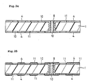
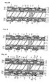
- numeral 1 is a substrate, numeral 2 an interlaminar insulating resin layer (an adhesive layer for electroless plating), numeral 2a an insulating layer, numeral 2b an adhesive layer, numeral 3 a plating resist, numeral 4 an inner layer conductor circuit (an inner layer copper pattern), numeral 5 an outer layer conductor circuit (an outer layer copper pattern), numeral 6 an opening for viahole, numeral 7 a viahole (BVH), numeral 8 a copper foil, numeral 9 a through-hole, numeral 10 a filling resin (a resin filler), numeral 11 a roughened layer, numeral 12 an electroless copper plated film, numeral 13 an electrolytic copper plated film, numeral 14 a solder resist layer, numeral 15 a nickel plated layer, numeral 16 a gold plated layer, numeral 17 a solder bump (a solder body), numeral 18 an alignment mark (used for positioning to a printed mask), numeral 19 an alignment mark (used for positioning to an IC chip mounting), numeral
- the printed circuit board according to the invention lies in a point that the conductor circuit is comprised of an electrolytic plated film and an electroless plated film, and the electroless plated film is located at an inner layer side and the electrolytic plated film is located at an outer layer side (see enlarged views of Fig. 18 and Fig. 19 ).
- the conductor circuit is able to follow to a size change of the interlaminar insulating resin layer as an upper layer even if warping of the board is generated in the heat cycle.
- the conductor circuit since the roughened layer is formed on the surface of the conductor circuit, the conductor circuit is strongly adhered to the interlaminar insulating resin layer as an upper layer and is more easy to follow to a size change of the interlaminar insulating resin layer.
- the roughened layer on at least a side face of the conductor circuit, which can control cracks generated in the interlaminar insulating resin layer starting from the boundary portion between the side face of the conductor circuit and the interlaminar resin contacted therewith.
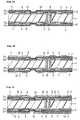
- the printed circuit board according to the invention lies in a point that the viahole is comprised of an electrolytic plated film and an electroless plated film, and the electroless plated film is located at an inner layer side and the electrolytic plated film is located at an outer layer side (see enlarged views of Fig. 18 and Fig. 19 ).
- the viahole in the printed circuit board according to the invention is constructed at the inner layer side with the hard electroless plated film and also such an electroless plated film is adhered to the under layer conductor circuit through the roughened layer, so that the viahole is not peeled off from the under layer conductor circuit in the heat cycle. Because the metal layer encroached by the roughened layer is the harder electroless plated film, and hence the breakage at the metal layer is hardly caused even when the peeling force is applied.
- the viahole when the viahole is comprised of only the electrolytic plated film, even if it is adhered to the under layer conductor circuit through the roughened layer, the electrolytic plated film itself is soft and is apt to peel off due to the heat cycle. While, when the viahole is comprised of only the electroless plated film, it can not follow to the size change of the interlaminar insulating resin layer and hence the crack is caused in the interlaminar insulating resin layer existing on the viahole.
- the viahole is comprised of the electrolytic plated film and the electroless plated film and connected to the under layer conductor circuit through the roughened layer, so that the occurence of cracks generated in the inter laminar insulating resin layer on the viahole, and the peeling between the viahole and the under layer conductor circuit in the heat cycle can be prevented at the same time.
- the interlaminar insulating resin layer is roughened, it is desirable that a plated film encroached into the roughened layer is hard. Because the breakage is hardly caused at the plated film portion when the peeling force is applied.
- the roughened layer may be formed on the surface of the viahole. Because the roughened layer is strongly adhered to the interlaminar insulating resin layer as an upper layer and hence the viahole is more easy to follow to the size change of the interlaminar insulating resin layer. Further, the roughened layer on the under layer conductor circuit may be formed on not only the portion connecting to the viahole but also the whole surface of the under layer conductor circuit. Because the adhesion property of the under layer conductor circuit to the interlaminar insulating resin layer is improved likewise the above structure 1.
- the under layer conductor circuit connecting to the viahole is comprised of the electrolytic plated film and the electroless plated film, and the electroless plated film is located at an inner layer side and the electrolytic plated film is located at an outer layer side. Because the inner layer side of the under layer conductor circuit is adhered to the interlaminar insulating resin layer, so that it is desirable to be a hard electroless plated film in order to ensure peel strength, while the contrary side is connected to the viahole and is desirable to be an electrolytic plated film having an excellent following property to the size change.
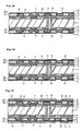
- the printed circuit board according to the invention lies in a point that the roughened layer is formed on at least a part of the surface of the conductor layer as an alignment mark used for positioning to a printed mask or an IC chip mounting and as an alignment mark used for mounting a packaged board obtained by mounting a semiconductor element onto another printed circuit board (see enlarged view of Fig. 41 ).
- the printed circuit board according to the invention lies in a point that the conductor layer as an alignment mark is comprised of the electrolytic plated film and the electroless plated film, and the electroless plated film is located at an inner layer side and the electrolytic plated film is located at an outer layer side, and the alignment mark is used for positioning to a printed mask or an IC chip mounting and for mounting the packaged board obtained by mounting a semiconductor element to another printed circuit board (see enlarged view of Fig. 41 ).
- the conductor layer is able to follow to the size change of the solder resist layer as an upper layer even if warping of the board is generated in a heat cycle. Moreover, when the roughened layer is formed on the surface of the conductor layer, the conductor layer is strongly adhered to the solder resist layer as an upper layer and is easy to follow to the size change of the solder resist layer. Further, the conductor contacting with the interlaminar insulating layer is an electroless plated film and high in the hardness, and hence a peel strength can be increased.
- the roughened layer on at least a side face of the conductor layer, which can control cracks generated in the solder resist layer or the like starting from a boundary between the side face of the conductor layer and the solder resist layer contacting therewith in the heat cycle.
- the metal layer made of nickel-gold is formed on the conductor layer as an alignment mark exposed from the opening portion. Because gold is high in the reflectance and advantageously functions as an alignment mark.
- the metal layer made of nickel-gold may be formed by electroless plating.
- the nickel layer is comprised of a nickel plated film having a thickness of 5 ⁇ m
- the gold layer is comprised of a flash gold plated film having a thickness of 0.1 ⁇ m or a thick gold plated film having a thickness of 0.5 ⁇ m.
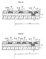
- the printed circuit board is comprised, for example, of an insulating substrate 1, a first layer conductor circuit 4 and an interlaminar insulating layer 2 (an adhesive layer for electroless plating) formed thereon, a pad (a conductor pattern) 21 for a solder bump formation composing a part of a second layer conductor circuit, an alignment mark 18 for positioning to a printed mask and an alignment mark 19 for an IC chip mounting formed on the interlaminar insulating agent 2 through semi-additive process, a solder resist layer 14 formed on a portion other than the alignment mark 18, 19 and the pad 21 for the solder bump formation.
- the alignment mark 18 for positioning to the printed mask is formed on a portion forming no conductor pattern in the vicinity of an outer peripheral portion of the printed circuit board. Concretely, it is formed, for example, on an outside of a product portion A shown in Fig. 41 . Therefore, the alignment mark 19 for the IC chip mounting enables an IC chip mounting without influence of the mark 18. In this case, the vicinity of the outer peripheral portion means an outside portion of the product portion as above mentioned. Further, the alignment mark 19 for the IC chip mounting is formed on each product portion in the printed circuit boards in order to mount an IC chip on each product portion. Further, in case of mounting a semiconductor element to produce a packaged board, the alignment mark 20 used for mounting the packaged board to another printed circuit board is formed on the innermost side as shown Fig. 42 . The alignment mark 20 is desirable to be a cross-shaped mark as shown Fig. 43 . In case of adopting the cross-shaped mark, an opening of a solder resist layer is formed so as to cover the peripheral edge of the cross.
- the alignment marks 18, 19 are preferable to be formed in the opening portions exposing only the surface of the conductor layer from the solder resist layer formed on the conductor layer (including the viahole). Because the peripheral edge of the conductor layer overlaps with the solder resist layer and hence the peeling of the conductor can be prevented by holding the conductor with the solder resist layer as shown Fig. 41 . Moreover, in the heat cycle, cracks generated starting from the boundary portion between the conductor layer and the interlaminar insulating resin layer due to the difference of thermal expansion coefficient can be controlled.
- the alignment mark for positioning to a printed mask has a following effect.
- the opening of the solder resist layer is formed by placing a photomask film and subjecting to light exposure and developing treatments. If the position of the photomask is shifted, the position of the opening is also shifted.
- the conductor layer as an alignment mark is perfectly exposed, since a center of the conductor is recognized as the central position of the alignment mark in a camera, the position shifting of the opening in the solder resist layer cannot be recognized. As a result, the opening portion of the printed mask is not coincident with the opening portion of the solder resist layer, so that an opening volume of the printed mask is decreased due to the solder resist layer and the height of a solder bump become low.
- the alignment mark is shifted to the same direction and amount as mentioned above.
- the opening portion of the printed mask is coincident with the opening portion of the solder resist layer, so that an opening volume of the printed mask is not decreased due to the solder resist layer and the height of a solder bump is not lowed.
- the pad 21 for the solder bump formation may be covered with the opening peripheral edge of the solder resist layer or may perfectly be exposed in the opening portion.
- the inner layer side of the conductor is constructed with the electroless plated film harder than the electrolytic plated film, and hence the peel strength is never lowered. Because the higher the hardness of the portion contacting with an interlaminar insulating layer and located in the inner layer side of the conductor circuit (in case of adopting an adhesive for electroless plating as mentioned later as an interlaminar insulating layer, the portion contacting with a roughened surface), the higher the peel strength.
- the printed circuit board having such a structures 1 ⁇ 4 can easily be produced by the production method according to the invention mentioned later (semi-additive process).
- the roughened layer formed on the surface of the conductor circuit, the surface of the viahole or the surface of the conductor layer for an alignment mark is a roughened surface of copper formed by an etching treatment, a polishing treatment, or a redox treatment, or a roughened surface of a plated film formed by subjecting to a plating treatment.
- the roughened layer is an alloy layer composed of copper-nickel-phosphorus. Because the alloy layer is a needle-shaped crystal layer and is excellent in the adhesion property to the solder resist layer. Further, the alloy layer is electrically conductive, and hence even if the solder body is formed on the surface of the pad, the removal of the alloy layer is not necessary.
- the composition of the alloy layer is desirable to be 90-96 wt% of copper, 1-5 wt% of nickel and 0.5-2 wt% of phosphorus because the needle-shaped structure is obtained in such a composition ratio.
- Fig. 18 is a triangular diagram of three components showing a composition of copper-nickel-phosphorus capable of forming the needle-shaped crystal.
- an oxidizing agent comprising sodium chlorite, sodium hydroxide and sodium phosphate.
- the roughened layer is formed by the redox treatment, it is desirably carried out by immersing a solution of a reducing agent comprising sodium hydroxide and sodium borohydride after the above oxidation treatment.
- the roughened layer formed on the surface of the conductor circuit is desirable to have a thickness of 0.5-10 ⁇ m, preferably 0.5-7 ⁇ m. Because, if the thickness is too thick, the roughened layer itself is apt to be damaged and peeled, while if it is too thin, the adhesion property lowers.
- the electroless plated film constituting the conductor circuit is desirable to have a thickness of 0.1-5 ⁇ m, preferably 0.5-3 ⁇ m. Because, if the thickness is too thick, the following property to the interlaminar insulating resin layer lowers, while if it is too thin, the degradation of peel strength is caused and the electric resistance becomes large in case of being subjected to an electrolytic plating to cause the scattering in the thickness of the plated film.
- the electrolytic plated film constituting the conductor circuit is desirable to have a thickness of 5-30 ⁇ m, preferably 10-20pm. Because, if the thickness is too thick, the degradation of peel strength is caused, while if it is too thin, the following property to the interlaminar insulating resin layer lowers.
- the conductor circuit is comprised of the electrolytic plated film and the electroless plated film, and the roughened layer formed on the surface of the conductor circuit mainly contacts with the electrolytic plated film.
- the electrolytic plated film is apt to be dissolved by the local electrode reaction as comparede with the electroless plated film, so that when the electrolytic plated film forms the local electrode with the roughened layer, it is rapidly dissolved and hence a large hole is apt to be formed in the surface of the conductor circuit.
- it is particularly desirable that the surface of the roughened layer is covered with a layer of a metal having an ionization tendency of more than copper but less than titanium or a noble metal, which is another feature in this point.
- the dissolution of the conductor circuit through the local electrode reaction can be controled.
- the metal having an ionization tendency not lower than that of copper but not higher than that of titanium there is at least one metal selected from the group consisting of titanium, aluminum, zinc, iron, indium, thallium, cobalt, nickel, tin, lead and bismuth.
- the noble metal there is at least one metal selected from the group consisting of gold, silver and platinum.
- Such a metal or noble metal layer covering the roughened layer can prevent the dissolution of the conductor circuit through the local electrode reaction caused in the roughening of the interlaminar insulating layer.
- Such a metal or noble metal layer is desirable to have a thickness of 0.1-2 ⁇ m.
- Tin is preferable. Tin can form a thin layer through an electroless substitution plating and can advantageously follow to the roughened layer.
- the roughened layer is formed on at least a side face of the conductor circuit. Because cracks generated in the interlaminar insulating resin layer due to the heat cycle result from the bad adhesion between the side face of the conductor circuit and the insulating resin layer, but in such a structure according to the invention, the cracks generated in the interlaminar insulating resin layer starting from the boundary between the side face of the conductor circuit and the insulating resin layer can be prevented.
- the adhesive for electroless plating is used as the interlaminar insulating resin layer constituting the above wiring substrate.
- the adhesive for electroless plating is optimum to be obtained by dispersing cured heat-resistant resin particles soluble in acid or oxidizing agent into an uncured heat-resistant resin hardly soluble in acid or oxidizing agent through curing.
- the heat-resistant resin particles can be dissolved and removed by treating with an acid or an oxidizing agent to form a roughened surface of octopus-trap shaped anchors on its surface.
- the cured heat-resistant resin particles are desirable to be selected from 1 heat-resistant resin powder having an average particle size of not more than 10 ⁇ m, 2 aggregated particles formed by aggregating heat-resistant resin powder having an average particle size of not more than 2 ⁇ m, 3 a mixture of heat-resistant resin powder having an average particle size of 2-10 ⁇ m and heat-resistant resin powder having an average particle size of not more than 2 ⁇ m, 4 false particles formed by adhering at least one of heat-resistant resin powder and inorganic powder having an average particle size of not more than 2 ⁇ m onto surfaces of heat-resistant resin powder having an average particle size of 2-10 ⁇ m, and 5 a mixture of heat-resistant resin powder having an average particle size of 0.1-0.8pm and heat-resistant resin powder having an average particle size of more than 0.8 ⁇ m but less than 2 ⁇ m because they can form complicated anchor.
- solder transferring method As a method of feeding the solder body, use may be made of a solder transferring method and a solder printing method.
- the solder transferring method is a method wherein a solder foil is attached to a prepreg and etched so as to leave only a portion corresponding to the opening portion to render into a solder carrier film having a solder pattern, and the solder carrier film is laminated so as to contact the solder pattern with the pad after a flux is applied to the opening portion in the solder resist of the substrate and heated to transfer the solder onto the pad.
- the solder printing method is a method wherein a metal mask having through-holes corresponding to the pads is placed onto the substrate and a solder paste is printed and heated.
- a multilayer printed circuit board having solder bumps is produced in the same manner as in Example 1 except that the roughening of the conductor circuit is carried out by etching.
- an etching solution of Durabond (trade name, made by Meck Co., Ltd.) is used.
- a multilayer printed circuit board having solder bumps is produced in the same manner as in Example 1 except that the roughening of the conductor circuit is carried out by etching.
- an etching solution of Durabond (trade name, made by Meck Co., Ltd.) is used.
- Au layer having a thickness of 0.5 ⁇ m is formed on the surface of the roughened layer by spputtering.
- a printed circuit board having solder bumps is produced in the same manner as in Example 5 except that a metal film is formed at the following conditions instead of tin substitution.
- a dry film photo-resist is laminated on the substrate treated in the step (1)-(8) of Example 1, and exposed and developed to form a plating resist. Then, after the step (9) of Example 1 is carried out, the plating resist is peeled and removed in the same manner as in the step (12) and the whole surface of the conductor circuit is roughened by the step (13) of Example 1. Thereafter, the formation of interlaminar insulating resin layer, roughening treatment, the formation of plating resist and electroless copper plating are carried out in the same manner as in Example 1, and after the plating resist is peeled and removed, a multilayer printed circuit board having solder bumps is produced by carrying the steps (15)-(19) of Example 1.
- the evaluation of these tests are carried out by confirming occurrences of cracks in the multilayer printed circuit board by means of a scanning electron microscope after the test. Further, the presence or absence of the peeling at the boundary between viahole and a lower conductor circuit layer is confirmed in the same manner. Furthermore, the peel strength is measured according to JIS-C-6481.
Landscapes
- Engineering & Computer Science (AREA)
- Microelectronics & Electronic Packaging (AREA)
- Manufacturing & Machinery (AREA)
- Manufacturing Of Printed Wiring (AREA)
- Production Of Multi-Layered Print Wiring Board (AREA)
- Structure Of Printed Boards (AREA)
Applications Claiming Priority (7)
| Application Number | Priority Date | Filing Date | Title |
|---|---|---|---|
| JP35497196 | 1996-12-19 | ||
| JP35795996A JPH10190224A (ja) | 1996-12-27 | 1996-12-27 | 多層プリント配線板およびその製造方法 |
| JP35780196 | 1996-12-28 | ||
| JP2958797A JPH10215060A (ja) | 1997-01-28 | 1997-01-28 | プリント配線板の半田バンプ形成方法、その形成方法において使用するプリント配線板および印刷用マスク |
| JP19752697A JPH10242638A (ja) | 1996-12-19 | 1997-07-23 | 多層プリント配線板およびその製造方法 |
| JP19752797A JPH10242639A (ja) | 1996-12-19 | 1997-07-23 | 多層プリント配線板およびその製造方法 |
| EP97949144A EP0952762B1 (fr) | 1996-12-19 | 1997-12-18 | Carte a circuit imprime et son procede de fabrication |
Related Parent Applications (2)
| Application Number | Title | Priority Date | Filing Date |
|---|---|---|---|
| EP97949144A Division EP0952762B1 (fr) | 1996-12-19 | 1997-12-18 | Carte a circuit imprime et son procede de fabrication |
| EP97949144.6 Division | 1998-06-25 |
Publications (3)
| Publication Number | Publication Date |
|---|---|
| EP1921902A2 true EP1921902A2 (fr) | 2008-05-14 |
| EP1921902A3 EP1921902A3 (fr) | 2009-03-25 |
| EP1921902B1 EP1921902B1 (fr) | 2011-03-02 |
Family
ID=27549470
Family Applications (2)
| Application Number | Title | Priority Date | Filing Date |
|---|---|---|---|
| EP08002134A Expired - Lifetime EP1921902B1 (fr) | 1996-12-19 | 1997-12-18 | Carte à circuit imprimé multicouche |
| EP97949144A Expired - Lifetime EP0952762B1 (fr) | 1996-12-19 | 1997-12-18 | Carte a circuit imprime et son procede de fabrication |
Family Applications After (1)
| Application Number | Title | Priority Date | Filing Date |
|---|---|---|---|
| EP97949144A Expired - Lifetime EP0952762B1 (fr) | 1996-12-19 | 1997-12-18 | Carte a circuit imprime et son procede de fabrication |
Country Status (7)
| Country | Link |
|---|---|
| US (11) | US6835895B1 (fr) |
| EP (2) | EP1921902B1 (fr) |
| KR (1) | KR20000057687A (fr) |
| CN (2) | CN100435605C (fr) |
| DE (1) | DE69740139D1 (fr) |
| MY (2) | MY128039A (fr) |
| WO (1) | WO1998027798A1 (fr) |
Families Citing this family (105)
| Publication number | Priority date | Publication date | Assignee | Title |
|---|---|---|---|---|
| EP1921902B1 (fr) * | 1996-12-19 | 2011-03-02 | Ibiden Co., Ltd. | Carte à circuit imprimé multicouche |
| US6141870A (en) | 1997-08-04 | 2000-11-07 | Peter K. Trzyna | Method for making electrical device |
| MY120077A (en) * | 1998-06-26 | 2005-08-30 | Ibiden Co Ltd | Multilayer printed wiring board having a roughened inner conductor layer and production method thereof |
| WO2000018202A1 (fr) * | 1998-09-17 | 2000-03-30 | Ibiden Co., Ltd. | Tableau de connexions multicouche d'accumulation |
| US6762921B1 (en) * | 1999-05-13 | 2004-07-13 | Ibiden Co., Ltd. | Multilayer printed-circuit board and method of manufacture |
| EP2086299A1 (fr) | 1999-06-02 | 2009-08-05 | Ibiden Co., Ltd. | Carte de circuit imprimé multicouches et procédé de fabrication d'une carte de circuit imprimé multicouches |
| JP4062907B2 (ja) * | 2001-11-12 | 2008-03-19 | 松下電器産業株式会社 | 回路基板およびその製造方法 |
| TWI227102B (en) * | 2002-03-15 | 2005-01-21 | United Test Ct Inc | Fabrication method for circuit carrier |
| US6596384B1 (en) * | 2002-04-09 | 2003-07-22 | International Business Machines Corporation | Selectively roughening conductors for high frequency printed wiring boards |
| TW550800B (en) * | 2002-05-27 | 2003-09-01 | Via Tech Inc | Integrated circuit package without solder mask and method for the same |
| JP2004031586A (ja) * | 2002-06-25 | 2004-01-29 | Sony Corp | 半導体装置の製造方法 |
| US7438969B2 (en) * | 2002-07-10 | 2008-10-21 | Ngk Spark Plug Co., Ltd. | Filling material, multilayer wiring board, and process of producing multilayer wiring board |
| US20050009415A1 (en) * | 2003-02-27 | 2005-01-13 | Johnson Morgan T. | Cable and connector assemblies and methods of making same |
| JP2004260074A (ja) * | 2003-02-27 | 2004-09-16 | Seiko Epson Corp | 半導体装置、半導体装置の製造方法及びその実装方法、回路基板並びに電子機器 |
| US8704359B2 (en) | 2003-04-01 | 2014-04-22 | Ge Embedded Electronics Oy | Method for manufacturing an electronic module and an electronic module |
| FI115601B (fi) * | 2003-04-01 | 2005-05-31 | Imbera Electronics Oy | Menetelmä elektroniikkamoduulin valmistamiseksi ja elektroniikkamoduuli |
| WO2004105454A1 (fr) * | 2003-05-23 | 2004-12-02 | Fujitsu Limited | Procede pour fabriquer un tableau de connexions |
| JP4516320B2 (ja) * | 2004-01-08 | 2010-08-04 | シチズン電子株式会社 | Led基板 |
| AT500807B1 (de) * | 2004-01-23 | 2006-11-15 | Austria Tech & System Tech | Verfahren zum herstellen eines leiterplattenelements sowie leiterplattenelement |
| GB0402960D0 (en) * | 2004-02-10 | 2004-03-17 | Plastic Logic Ltd | Thermal imaging of catalyst in electroless deposition of metal films |
| JP3804803B2 (ja) * | 2004-02-12 | 2006-08-02 | 沖電気工業株式会社 | 電子部品搭載用基板及び半導体装置 |
| JP4361826B2 (ja) * | 2004-04-20 | 2009-11-11 | 新光電気工業株式会社 | 半導体装置 |
| US7307022B2 (en) * | 2004-11-19 | 2007-12-11 | Endicott Interconnect Technologies, Inc. | Method of treating conductive layer for use in a circuitized substrate and method of making said substrate having said conductive layer as part thereof |
| US7583834B2 (en) * | 2005-03-04 | 2009-09-01 | Eastman Kodak Company | Laser etched fiducials in roll-roll display |
| JP4646661B2 (ja) * | 2005-03-18 | 2011-03-09 | 株式会社リコー | プリント配線基板印刷方法と実装方法ならびにプログラム |
| US7170183B1 (en) * | 2005-05-13 | 2007-01-30 | Amkor Technology, Inc. | Wafer level stacked package |
| JP4146864B2 (ja) * | 2005-05-31 | 2008-09-10 | 新光電気工業株式会社 | 配線基板及びその製造方法、並びに半導体装置及び半導体装置の製造方法 |
| TWI294757B (en) * | 2005-07-06 | 2008-03-11 | Delta Electronics Inc | Circuit board with a through hole wire, and forming method thereof |
| JP4123251B2 (ja) * | 2005-07-07 | 2008-07-23 | セイコーエプソン株式会社 | 半導体装置製造用基板、半導体装置の製造方法 |
| JP2007129124A (ja) * | 2005-11-07 | 2007-05-24 | Matsushita Electric Ind Co Ltd | 多層プリント配線基板及びその製造方法 |
| US9486408B2 (en) | 2005-12-01 | 2016-11-08 | University Of Massachusetts Lowell | Botulinum nanoemulsions |
| US7906850B2 (en) * | 2005-12-20 | 2011-03-15 | Unimicron Technology Corp. | Structure of circuit board and method for fabricating same |
| JP4656318B2 (ja) * | 2006-01-31 | 2011-03-23 | ミツミ電機株式会社 | アンテナ装置 |
| CN101466869A (zh) * | 2006-06-16 | 2009-06-24 | 乔治洛德方法研究和开发液化空气有限公司 | 用于铜互连层的无电镀NiP附着和/或覆盖层 |
| US7538429B2 (en) * | 2006-08-21 | 2009-05-26 | Intel Corporation | Method of enabling solder deposition on a substrate and electronic package formed thereby |
| SG177184A1 (en) | 2006-12-01 | 2012-01-30 | Anterios Inc | Amphiphilic entity nanoparticles |
| SG179457A1 (en) | 2006-12-01 | 2012-04-27 | Anterios Inc | Peptide nanoparticles and uses therefor |
| CN101543144B (zh) * | 2007-03-14 | 2012-12-05 | 松下电器产业株式会社 | 识别标志以及电路基板的制造方法 |
| TW200906263A (en) * | 2007-05-29 | 2009-02-01 | Matsushita Electric Industrial Co Ltd | Circuit board and method for manufacturing the same |
| JP4588046B2 (ja) * | 2007-05-31 | 2010-11-24 | 三洋電機株式会社 | 回路装置およびその製造方法 |
| CN101765423B (zh) | 2007-05-31 | 2014-08-06 | 安特里奥公司 | 核酸纳米粒子和其用途 |
| US8647517B2 (en) * | 2007-07-09 | 2014-02-11 | Nitto Denko Corporation | Producing method of suspension board with circuit |
| US8238114B2 (en) * | 2007-09-20 | 2012-08-07 | Ibiden Co., Ltd. | Printed wiring board and method for manufacturing same |
| JP2009099624A (ja) * | 2007-10-12 | 2009-05-07 | Fujitsu Ltd | 配線基板およびその製造方法 |
| US9439293B2 (en) * | 2007-11-21 | 2016-09-06 | Xerox Corporation | Galvanic process for making printed conductive metal markings for chipless RFID applications |
| US8314348B2 (en) * | 2008-03-03 | 2012-11-20 | Ibiden Co., Ltd. | Multilayer printed wiring board and method of manufacturing multilayer printed wiring board |
| US7749814B2 (en) * | 2008-03-13 | 2010-07-06 | Stats Chippac, Ltd. | Semiconductor device with integrated passive circuit and method of making the same using sacrificial substrate |
| JP2009260216A (ja) * | 2008-03-19 | 2009-11-05 | Shinko Electric Ind Co Ltd | 配線基板の製造方法 |
| US8132321B2 (en) * | 2008-08-13 | 2012-03-13 | Unimicron Technology Corp. | Method for making embedded circuit structure |
| JP2010087229A (ja) * | 2008-09-30 | 2010-04-15 | Sanyo Electric Co Ltd | 半導体モジュール、半導体モジュールの製造方法および携帯機器 |
| KR101022912B1 (ko) * | 2008-11-28 | 2011-03-17 | 삼성전기주식회사 | 금속범프를 갖는 인쇄회로기판 및 그 제조방법 |
| US8921705B2 (en) * | 2008-11-28 | 2014-12-30 | Ibiden Co., Ltd. | Wiring board and fabrication method therefor |
| US20100139967A1 (en) * | 2008-12-08 | 2010-06-10 | Ibiden Co., Ltd. | Wiring board and fabrication method therefor |
| JP5142967B2 (ja) * | 2008-12-10 | 2013-02-13 | ルネサスエレクトロニクス株式会社 | 半導体装置 |
| TW201037803A (en) * | 2009-04-13 | 2010-10-16 | High Conduction Scient Co Ltd | Multi-layer packaging substrate, method for making the packaging substrate, and package structure of light-emitting semiconductor |
| US8076776B2 (en) | 2009-06-16 | 2011-12-13 | Intel Corporation | Integrated circuit package having security feature and method of manufacturing same |
| US8161637B2 (en) * | 2009-07-24 | 2012-04-24 | Ibiden Co., Ltd. | Manufacturing method for printed wiring board |
| JP5428667B2 (ja) * | 2009-09-07 | 2014-02-26 | 日立化成株式会社 | 半導体チップ搭載用基板の製造方法 |
| KR101070098B1 (ko) * | 2009-09-15 | 2011-10-04 | 삼성전기주식회사 | 인쇄회로기판 및 그의 제조 방법 |
| KR101070022B1 (ko) * | 2009-09-16 | 2011-10-04 | 삼성전기주식회사 | 다층 세라믹 회로 기판, 다층 세라믹 회로 기판 제조방법 및 이를 이용한 전자 디바이스 모듈 |
| JP5627097B2 (ja) * | 2009-10-07 | 2014-11-19 | ルネサスエレクトロニクス株式会社 | 配線基板 |
| JP5603600B2 (ja) * | 2010-01-13 | 2014-10-08 | 新光電気工業株式会社 | 配線基板及びその製造方法、並びに半導体パッケージ |
| US8581104B2 (en) * | 2010-03-31 | 2013-11-12 | Ibiden Co., Ltd. | Wiring board and method for manufacturing the same |
| US20120211370A1 (en) * | 2011-02-22 | 2012-08-23 | Ibiden Co., Ltd. | Method for manufacturing wiring board |
| JP5856288B2 (ja) | 2011-04-29 | 2016-02-09 | インターコンチネンタル グレート ブランズ エルエルシー | 封入酸、封入酸の調製方法、および封入酸を含むチューインガム |
| TWI430717B (zh) * | 2011-07-15 | 2014-03-11 | 光寶電子(廣州)有限公司 | 基板結構、半導體裝置陣列及其半導體裝置 |
| US20130168132A1 (en) * | 2011-12-29 | 2013-07-04 | Sumsung Electro-Mechanics Co., Ltd. | Printed circuit board and method of manufacturing the same |
| JP5966874B2 (ja) * | 2012-01-27 | 2016-08-10 | Tdk株式会社 | 構造体、及びそれを含む電子部品、プリント配線板 |
| KR20130113376A (ko) * | 2012-04-05 | 2013-10-15 | 타이코에이엠피(유) | 인쇄회로기판 및 그 제조방법 |
| CN103379726A (zh) * | 2012-04-17 | 2013-10-30 | 景硕科技股份有限公司 | 线路积层板的复层线路结构 |
| WO2013168761A1 (fr) * | 2012-05-10 | 2013-11-14 | 日立化成株式会社 | Carte de circuits à couches multiples |
| KR101523840B1 (ko) * | 2012-08-30 | 2015-05-28 | 이비덴 가부시키가이샤 | 프린트 배선판 및 프린트 배선판의 제조 방법 |
| JP5990438B2 (ja) * | 2012-09-13 | 2016-09-14 | ルネサスエレクトロニクス株式会社 | 半導体装置の製造方法 |
| US8847078B2 (en) * | 2012-09-27 | 2014-09-30 | Ibiden Co., Ltd. | Printed wiring board and method for manufacturing printed wiring board |
| KR20140060767A (ko) * | 2012-11-12 | 2014-05-21 | 삼성전기주식회사 | 회로 기판 및 그 제조 방법 |
| CN103906371B (zh) * | 2012-12-27 | 2017-09-19 | 碁鼎科技秦皇岛有限公司 | 具有内埋元件的电路板及其制作方法 |
| WO2014140047A2 (fr) | 2013-03-12 | 2014-09-18 | Micronic Mydata AB | Procédé et dispositif d'écriture de masques photographiques avec réduction des erreurs mura |
| KR102253995B1 (ko) | 2013-03-12 | 2021-05-18 | 마이크로닉 아베 | 기계적으로 생성된 정렬 표식 방법 및 정렬 시스템 |
| KR20140123273A (ko) * | 2013-04-12 | 2014-10-22 | 타이코에이엠피(유) | 인쇄회로기판 및 그 제조방법 |
| JP5754464B2 (ja) * | 2013-05-21 | 2015-07-29 | 株式会社村田製作所 | モジュールおよびその製造方法 |
| JP6266907B2 (ja) * | 2013-07-03 | 2018-01-24 | 新光電気工業株式会社 | 配線基板及び配線基板の製造方法 |
| JP2015023251A (ja) * | 2013-07-23 | 2015-02-02 | ソニー株式会社 | 多層配線基板およびその製造方法、並びに半導体製品 |
| JP6163446B2 (ja) * | 2014-03-27 | 2017-07-12 | 株式会社東芝 | 半導体装置の製造方法 |
| JP2015231003A (ja) * | 2014-06-06 | 2015-12-21 | イビデン株式会社 | 回路基板および回路基板の製造方法 |
| US9520352B2 (en) * | 2014-12-10 | 2016-12-13 | Shinko Electric Industries Co., Ltd. | Wiring board and semiconductor device |
| JP2016207893A (ja) * | 2015-04-24 | 2016-12-08 | イビデン株式会社 | プリント配線板およびその製造方法 |
| US20170064821A1 (en) * | 2015-08-31 | 2017-03-02 | Kristof Darmawikarta | Electronic package and method forming an electrical package |
| JP2017059707A (ja) * | 2015-09-17 | 2017-03-23 | 富士通株式会社 | 積層チップ、積層チップを搭載する基板、及び積層チップの製造方法 |
| US9831147B2 (en) * | 2015-11-30 | 2017-11-28 | Infineon Technologies Austria Ag | Packaged semiconductor device with internal electrical connections to outer contacts |
| MX2019005833A (es) | 2016-11-21 | 2019-10-30 | Eirion Therapeutics Inc | Administracion transdermica de agentes grandes. |
| TWI680473B (zh) * | 2017-01-13 | 2019-12-21 | 日商利特弗日本合同公司 | 機器及防止機器不良的方法 |
| CA3047703C (fr) * | 2017-02-09 | 2023-04-25 | Fluor Technologies Corporation | Absorption en deux etapes pour elimination de gaz acide et de mercaptan |
| FR3065617B1 (fr) * | 2017-04-20 | 2022-01-21 | Auxel | Procede de fabrication d'un circuit multicouches pour la distribution de courant electrique |
| FR3065616B1 (fr) * | 2017-04-20 | 2019-09-06 | Auxel | Procede de fabrication d'un circuit multicouches |
| TWI645483B (zh) * | 2017-06-30 | 2018-12-21 | 同泰電子科技股份有限公司 | 適於形成包括通孔的基板結構的製作方法 |
| JP7139594B2 (ja) * | 2017-11-30 | 2022-09-21 | 凸版印刷株式会社 | ガラスコア、多層配線基板、及びガラスコアの製造方法 |
| TWI665455B (zh) * | 2018-05-30 | 2019-07-11 | 緯穎科技服務股份有限公司 | 用於傳輸並供測試高速訊號的電路板 |
| JP6733941B1 (ja) | 2019-03-22 | 2020-08-05 | 大口マテリアル株式会社 | 半導体素子搭載用基板 |
| JP6736719B1 (ja) * | 2019-03-28 | 2020-08-05 | 大口マテリアル株式会社 | 半導体素子搭載用部品、リードフレーム及び半導体素子搭載用基板 |
| KR102875198B1 (ko) | 2019-08-19 | 2025-10-22 | 아토테크 도이칠란트 게엠베하 운트 콤파니 카게 | 구리로 충전된 마이크로비아들을 포함하는 고밀도 상호연결 인쇄 회로 기판을 제조하는 방법 |
| TWI703903B (zh) * | 2019-12-19 | 2020-09-01 | 頎邦科技股份有限公司 | 可撓性電路板 |
| CN113411962A (zh) * | 2020-03-17 | 2021-09-17 | 广州方邦电子股份有限公司 | 埋阻金属箔、印制板以及埋阻金属箔的制备方法 |
| TWI715492B (zh) * | 2020-05-08 | 2021-01-01 | 頎邦科技股份有限公司 | 線路板 |
| US11842958B2 (en) * | 2022-03-18 | 2023-12-12 | Chun-Ming Lin | Conductive structure including copper-phosphorous alloy and a method of manufacturing conductive structure |
| US12087662B1 (en) | 2023-06-12 | 2024-09-10 | Chun-Ming Lin | Semiconductor package structure having thermal management structure |
Citations (2)
| Publication number | Priority date | Publication date | Assignee | Title |
|---|---|---|---|---|
| JPH0455555B2 (fr) | 1986-11-14 | 1992-09-03 | Ibiden Co Ltd | |
| JPH06283860A (ja) | 1993-01-26 | 1994-10-07 | Ibiden Co Ltd | 多層プリント配線板およびその製造方法 |
Family Cites Families (71)
| Publication number | Priority date | Publication date | Assignee | Title |
|---|---|---|---|---|
| US3612743A (en) * | 1970-10-13 | 1971-10-12 | Nasa | Shielded flat cable |
| US3935041A (en) | 1971-10-18 | 1976-01-27 | Chemcut Corporation | Method for treatment fluid application and removal |
| US3791858A (en) | 1971-12-13 | 1974-02-12 | Ibm | Method of forming multi-layer circuit panels |
| US3996416A (en) | 1975-03-18 | 1976-12-07 | Amp Incorporated | Interconnection system and method of assembly |
| US3996415A (en) * | 1975-07-03 | 1976-12-07 | Clifford Provorse | Easy to install telephone service bracket |
| US4017968A (en) * | 1975-09-18 | 1977-04-19 | Jerobee Industries, Inc. | Method of making plated through hole printed circuit board |
| US4258468A (en) | 1978-12-14 | 1981-03-31 | Western Electric Company, Inc. | Forming vias through multilayer circuit boards |
| US4510276A (en) | 1979-12-13 | 1985-04-09 | Kollmorgen Technologies Corporation | Epoxy resin coating compositions for printed circuit boards |
| JPS5851436B2 (ja) * | 1980-02-29 | 1983-11-16 | 株式会社東芝 | プリント回路板の製造方法 |
| CA1178996A (fr) | 1981-08-17 | 1984-12-04 | Charles W. Daggett | Bloc porte-fusible |
| US4706167A (en) | 1983-11-10 | 1987-11-10 | Telemark Co., Inc. | Circuit wiring disposed on solder mask coating |
| US4628598A (en) * | 1984-10-02 | 1986-12-16 | The United States Of America As Represented By The Secretary Of The Air Force | Mechanical locking between multi-layer printed wiring board conductors and through-hole plating |
| JPS61229389A (ja) | 1985-04-03 | 1986-10-13 | イビデン株式会社 | セラミツク配線板およびその製造方法 |
| CN1003524B (zh) | 1985-10-14 | 1989-03-08 | 株式会社日立制作所 | 无电浸镀金溶液 |
| US5322976A (en) * | 1987-02-24 | 1994-06-21 | Polyonics Corporation | Process for forming polyimide-metal laminates |
| JPH0644669B2 (ja) | 1987-10-31 | 1994-06-08 | イビデン株式会社 | 表面実装部品搭載用プリント配線板 |
| DE3913966B4 (de) | 1988-04-28 | 2005-06-02 | Ibiden Co., Ltd., Ogaki | Klebstoffdispersion zum stromlosen Plattieren, sowie Verwendung zur Herstellung einer gedruckten Schaltung |
| JPH0289633A (ja) | 1988-05-20 | 1990-03-29 | Sumitomo Electric Ind Ltd | フッ素樹脂被覆物 |
| JPH0634448B2 (ja) | 1988-07-25 | 1994-05-02 | 株式会社日立製作所 | 多層プリント配線板及びその製造方法 |
| JPH0628941B2 (ja) * | 1988-09-20 | 1994-04-20 | 株式会社日立製作所 | 回路基板及びその製造方法 |
| US4978423A (en) | 1988-09-26 | 1990-12-18 | At&T Bell Laboratories | Selective solder formation on printed circuit boards |
| JPH02197148A (ja) | 1989-01-26 | 1990-08-03 | Nec Corp | 多層配線基板における配線形成方法 |
| JP3069356B2 (ja) | 1989-05-31 | 2000-07-24 | イビデン株式会社 | 多層プリント配線板およびその製造方法 |
| JPH045844A (ja) * | 1990-04-23 | 1992-01-09 | Nippon Mektron Ltd | Ic搭載用多層回路基板及びその製造法 |
| JPH0455555A (ja) | 1990-06-25 | 1992-02-24 | Misawa Homes Co Ltd | 建物の手摺支柱の設置構造 |
| US5156732A (en) | 1990-07-11 | 1992-10-20 | Sumitomo Metal Mining Co. Ltd. | Polyimide substrate and method of manufacturing a printed wiring board using the substrate |
| JPH04122012A (ja) | 1990-09-12 | 1992-04-22 | Mitsubishi Electric Corp | アライメントマークおよびその形成方法 |
| US5298685A (en) | 1990-10-30 | 1994-03-29 | International Business Machines Corporation | Interconnection method and structure for organic circuit boards |
| US5861076A (en) | 1991-07-19 | 1999-01-19 | Park Electrochemical Corporation | Method for making multi-layer circuit boards |
| GB2258183A (en) | 1991-08-01 | 1993-02-03 | Motorola Inc | Solder mask defined printed circuit board |
| US5209817A (en) | 1991-08-22 | 1993-05-11 | International Business Machines Corporation | Selective plating method for forming integral via and wiring layers |
| JPH05283334A (ja) | 1991-12-04 | 1993-10-29 | Toshiba Corp | 金属配線層の平坦化方法および平坦化装置 |
| JPH05304362A (ja) | 1992-04-28 | 1993-11-16 | Murata Mfg Co Ltd | 多層配線板の製造方法 |
| US5517758A (en) * | 1992-05-29 | 1996-05-21 | Matsushita Electric Industrial Co., Ltd. | Plating method and method for producing a multi-layered printed wiring board using the same |
| JP3361556B2 (ja) | 1992-09-25 | 2003-01-07 | 日本メクトロン株式会社 | 回路配線パタ−ンの形成法 |
| JP2819523B2 (ja) | 1992-10-09 | 1998-10-30 | インターナショナル・ビジネス・マシーンズ・コーポレイション | 印刷配線板及びその製造方法 |
| JP2790956B2 (ja) | 1993-03-03 | 1998-08-27 | 株式会社日立製作所 | 多層配線板の製法 |
| DE69407467T2 (de) | 1993-04-12 | 1998-04-16 | Ibiden Co Ltd | Harzzusammensetzungen und diese verwendende Leiterplatten |
| JP2790416B2 (ja) | 1993-08-26 | 1998-08-27 | 沖電気工業株式会社 | アライメントマーク配置方法 |
| JPH07147483A (ja) | 1993-09-30 | 1995-06-06 | Ibiden Co Ltd | プリント配線板及びその製造方法 |
| JP3536152B2 (ja) | 1993-10-14 | 2004-06-07 | イビデン株式会社 | プリント配線板 |
| US5527998A (en) | 1993-10-22 | 1996-06-18 | Sheldahl, Inc. | Flexible multilayer printed circuit boards and methods of manufacture |
| JP2694802B2 (ja) | 1993-12-28 | 1997-12-24 | 日本電気株式会社 | プリント配線板の製造方法 |
| JPH07249558A (ja) | 1994-03-09 | 1995-09-26 | Nikon Corp | 位置合わせ方法 |
| JP3527965B2 (ja) | 1994-03-29 | 2004-05-17 | イビデン株式会社 | プリント配線板 |
| JPH07273439A (ja) | 1994-03-31 | 1995-10-20 | Du Pont Kk | 半田バンプ形成方法 |
| JPH0823160A (ja) * | 1994-05-06 | 1996-01-23 | Seiko Epson Corp | プリント配線板と電子部品の接続方法 |
| US5495667A (en) | 1994-11-07 | 1996-03-05 | Micron Technology, Inc. | Method for forming contact pins for semiconductor dice and interconnects |
| JP3637613B2 (ja) | 1994-11-10 | 2005-04-13 | 日立化成工業株式会社 | 多層配線板の製造方法 |
| US5745333A (en) * | 1994-11-21 | 1998-04-28 | International Business Machines Corporation | Laminar stackable circuit board structure with capacitor |
| US5929741A (en) | 1994-11-30 | 1999-07-27 | Hitachi Chemical Company, Ltd. | Current protector |
| CN1117512C (zh) | 1994-12-01 | 2003-08-06 | 揖斐电株式会社 | 多层印刷电路板及其制造方法 |
| JP3694796B2 (ja) * | 1994-12-12 | 2005-09-14 | イビデン株式会社 | プリント配線板及びその製造方法 |
| JPH08181436A (ja) | 1994-12-21 | 1996-07-12 | Sumitomo Bakelite Co Ltd | 感光性アディティブ接着剤を用いた多層プリント配線板の製造方法 |
| JPH08181438A (ja) | 1994-12-22 | 1996-07-12 | Sumitomo Bakelite Co Ltd | 感光性アディティブ接着剤を用いた多層プリント配線板の製造方法 |
| US5466349A (en) | 1995-01-06 | 1995-11-14 | Rockwell International Corporation | Potentiometric evaluation of substrate oxidation and coating porosity |
| JPH08242064A (ja) | 1995-03-01 | 1996-09-17 | Ibiden Co Ltd | プリント配線板 |
| JPH08250857A (ja) * | 1995-03-07 | 1996-09-27 | Murata Mfg Co Ltd | 多層配線基板の製造方法 |
| JP3174474B2 (ja) | 1995-03-24 | 2001-06-11 | イビデン株式会社 | プリント配線板の製造方法 |
| JPH08279682A (ja) | 1995-04-05 | 1996-10-22 | Asahi Denka Kogyo Kk | 多層回路基板の製造方法 |
| JP3420391B2 (ja) | 1995-06-20 | 2003-06-23 | キヤノン株式会社 | 電気回路基板におけるアライメントマーク構造 |
| US5699613A (en) | 1995-09-25 | 1997-12-23 | International Business Machines Corporation | Fine dimension stacked vias for a multiple layer circuit board structure |
| US5648125A (en) | 1995-11-16 | 1997-07-15 | Cane; Frank N. | Electroless plating process for the manufacture of printed circuit boards |
| US5826330A (en) * | 1995-12-28 | 1998-10-27 | Hitachi Aic Inc. | Method of manufacturing multilayer printed wiring board |
| US5993945A (en) | 1996-05-30 | 1999-11-30 | International Business Machines Corporation | Process for high resolution photoimageable dielectric |
| TW331698B (en) | 1996-06-18 | 1998-05-11 | Hitachi Chemical Co Ltd | Multi-layered printed circuit board |
| US5827064A (en) | 1996-08-30 | 1998-10-27 | Sonex International Corp. | Orbitally or reciprocally vibrating method for interproximal plaque removal |
| EP1796446B1 (fr) * | 1996-11-20 | 2011-05-11 | Ibiden Co., Ltd. | Circuit imprimé |
| JP2003060342A (ja) | 1996-12-19 | 2003-02-28 | Ibiden Co Ltd | 多層プリント配線板およびその製造方法 |
| EP1921902B1 (fr) | 1996-12-19 | 2011-03-02 | Ibiden Co., Ltd. | Carte à circuit imprimé multicouche |
| US6204454B1 (en) | 1997-12-27 | 2001-03-20 | Tdk Corporation | Wiring board and process for the production thereof |
-
1997
- 1997-12-18 EP EP08002134A patent/EP1921902B1/fr not_active Expired - Lifetime
- 1997-12-18 CN CNB2004101000753A patent/CN100435605C/zh not_active Expired - Lifetime
- 1997-12-18 US US09/319,258 patent/US6835895B1/en not_active Ceased
- 1997-12-18 MY MYPI20043243A patent/MY128039A/en unknown
- 1997-12-18 US US11/595,000 patent/USRE43509E1/en not_active Expired - Lifetime
- 1997-12-18 CN CNB971814473A patent/CN1265691C/zh not_active Expired - Lifetime
- 1997-12-18 EP EP97949144A patent/EP0952762B1/fr not_active Expired - Lifetime
- 1997-12-18 DE DE69740139T patent/DE69740139D1/de not_active Expired - Lifetime
- 1997-12-18 WO PCT/JP1997/004684 patent/WO1998027798A1/fr not_active Ceased
- 1997-12-18 KR KR1019990705543A patent/KR20000057687A/ko not_active Ceased
- 1997-12-18 MY MYPI97006160A patent/MY125599A/en unknown
-
2003
- 2003-01-27 US US10/351,501 patent/US6930255B2/en not_active Expired - Lifetime
-
2005
- 2005-08-15 US US11/203,427 patent/US7449791B2/en not_active Expired - Fee Related
-
2006
- 2006-09-19 US US11/522,960 patent/US7615162B2/en not_active Expired - Fee Related
- 2006-09-19 US US11/522,999 patent/US7388159B2/en not_active Expired - Fee Related
- 2006-09-19 US US11/522,961 patent/US7712212B2/en not_active Expired - Fee Related
- 2006-09-19 US US11/523,000 patent/US7385146B2/en not_active Expired - Fee Related
- 2006-09-19 US US11/522,938 patent/US7585541B2/en not_active Expired - Fee Related
- 2006-09-19 US US11/522,956 patent/US7361849B2/en not_active Expired - Fee Related
- 2006-09-19 US US11/522,940 patent/US7371976B2/en not_active Expired - Fee Related
Patent Citations (2)
| Publication number | Priority date | Publication date | Assignee | Title |
|---|---|---|---|---|
| JPH0455555B2 (fr) | 1986-11-14 | 1992-09-03 | Ibiden Co Ltd | |
| JPH06283860A (ja) | 1993-01-26 | 1994-10-07 | Ibiden Co Ltd | 多層プリント配線板およびその製造方法 |
Also Published As
Similar Documents
| Publication | Publication Date | Title |
|---|---|---|
| EP0952762B1 (fr) | Carte a circuit imprime et son procede de fabrication | |
| EP0844809B1 (fr) | Composition d'un masque de soudure et des panneaux à circuit imprimé | |
| EP1005261B1 (fr) | Adhesif utile pour effectuer le depot autocatalytique, composition de produit de depart utile pour preparer de l'adhesif pour depot catalytique et carte imprimee | |
| EP0999731A1 (fr) | Carte a circuits imprimes et procede de fabrication de ladite carte | |
| US6248428B1 (en) | Adhesive for electroless plating, raw material composition for preparing adhesive for electroless plating and printed wiring board | |
| JP3152633B2 (ja) | 多層プリント配線板およびその製造方法 | |
| JP3098729B2 (ja) | 多層プリント配線板の製造方法 | |
| JP3299243B2 (ja) | 多層プリント配線板の製造方法 | |
| JPH10242639A (ja) | 多層プリント配線板およびその製造方法 | |
| JPH10242638A (ja) | 多層プリント配線板およびその製造方法 | |
| JP2007227959A (ja) | 多層プリント配線板およびその製造方法 | |
| JP2003060342A (ja) | 多層プリント配線板およびその製造方法 | |
| JPH10242640A (ja) | プリント配線板 |
Legal Events
| Date | Code | Title | Description |
|---|---|---|---|
| PUAI | Public reference made under article 153(3) epc to a published international application that has entered the european phase |
Free format text: ORIGINAL CODE: 0009012 |
|
| 17P | Request for examination filed |
Effective date: 20080205 |
|
| AC | Divisional application: reference to earlier application |
Ref document number: 0952762 Country of ref document: EP Kind code of ref document: P |
|
| AK | Designated contracting states |
Kind code of ref document: A2 Designated state(s): DE FI GB NL |
|
| PUAL | Search report despatched |
Free format text: ORIGINAL CODE: 0009013 |
|
| AK | Designated contracting states |
Kind code of ref document: A3 Designated state(s): DE FI GB NL |
|
| AKX | Designation fees paid |
Designated state(s): DE FI GB NL |
|
| RTI1 | Title (correction) |
Free format text: MULTILAYERED PRINTED CIRCUIT BOARD |
|
| GRAP | Despatch of communication of intention to grant a patent |
Free format text: ORIGINAL CODE: EPIDOSNIGR1 |
|
| RAP1 | Party data changed (applicant data changed or rights of an application transferred) |
Owner name: IBIDEN CO., LTD. |
|
| GRAS | Grant fee paid |
Free format text: ORIGINAL CODE: EPIDOSNIGR3 |
|
| GRAA | (expected) grant |
Free format text: ORIGINAL CODE: 0009210 |
|
| AC | Divisional application: reference to earlier application |
Ref document number: 0952762 Country of ref document: EP Kind code of ref document: P |
|
| AK | Designated contracting states |
Kind code of ref document: B1 Designated state(s): DE FI GB NL |
|
| REG | Reference to a national code |
Ref country code: GB Ref legal event code: FG4D |
|
| REF | Corresponds to: |
Ref document number: 69740139 Country of ref document: DE Date of ref document: 20110414 Kind code of ref document: P |
|
| REG | Reference to a national code |
Ref country code: DE Ref legal event code: R096 Ref document number: 69740139 Country of ref document: DE Effective date: 20110414 |
|
| REG | Reference to a national code |
Ref country code: NL Ref legal event code: VDEP Effective date: 20110302 |
|
| PG25 | Lapsed in a contracting state [announced via postgrant information from national office to epo] |
Ref country code: NL Free format text: LAPSE BECAUSE OF FAILURE TO SUBMIT A TRANSLATION OF THE DESCRIPTION OR TO PAY THE FEE WITHIN THE PRESCRIBED TIME-LIMIT Effective date: 20110302 Ref country code: FI Free format text: LAPSE BECAUSE OF FAILURE TO SUBMIT A TRANSLATION OF THE DESCRIPTION OR TO PAY THE FEE WITHIN THE PRESCRIBED TIME-LIMIT Effective date: 20110302 |
|
| PLBE | No opposition filed within time limit |
Free format text: ORIGINAL CODE: 0009261 |
|
| STAA | Information on the status of an ep patent application or granted ep patent |
Free format text: STATUS: NO OPPOSITION FILED WITHIN TIME LIMIT |
|
| 26N | No opposition filed |
Effective date: 20111205 |
|
| REG | Reference to a national code |
Ref country code: DE Ref legal event code: R097 Ref document number: 69740139 Country of ref document: DE Effective date: 20111205 |
|
| PGFP | Annual fee paid to national office [announced via postgrant information from national office to epo] |
Ref country code: DE Payment date: 20161213 Year of fee payment: 20 Ref country code: GB Payment date: 20161214 Year of fee payment: 20 |
|
| REG | Reference to a national code |
Ref country code: DE Ref legal event code: R071 Ref document number: 69740139 Country of ref document: DE |
|
| REG | Reference to a national code |
Ref country code: GB Ref legal event code: PE20 Expiry date: 20171217 |
|
| PG25 | Lapsed in a contracting state [announced via postgrant information from national office to epo] |
Ref country code: GB Free format text: LAPSE BECAUSE OF EXPIRATION OF PROTECTION Effective date: 20171217 |