EP2680193A1 - Dispositif avec circuit RFID - Google Patents
Dispositif avec circuit RFID Download PDFInfo
- Publication number
- EP2680193A1 EP2680193A1 EP20130186179 EP13186179A EP2680193A1 EP 2680193 A1 EP2680193 A1 EP 2680193A1 EP 20130186179 EP20130186179 EP 20130186179 EP 13186179 A EP13186179 A EP 13186179A EP 2680193 A1 EP2680193 A1 EP 2680193A1
- Authority
- EP
- European Patent Office
- Prior art keywords
- radio
- electrode
- feed circuit
- disposed
- radiation plate
- Prior art date
- Legal status (The legal status is an assumption and is not a legal conclusion. Google has not performed a legal analysis and makes no representation as to the accuracy of the status listed.)
- Granted
Links
Images











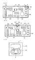

Classifications
-
- G—PHYSICS
- G06—COMPUTING OR CALCULATING; COUNTING
- G06K—GRAPHICAL DATA READING; PRESENTATION OF DATA; RECORD CARRIERS; HANDLING RECORD CARRIERS
- G06K19/00—Record carriers for use with machines and with at least a part designed to carry digital markings
- G06K19/06—Record carriers for use with machines and with at least a part designed to carry digital markings characterised by the kind of the digital marking, e.g. shape, nature, code
- G06K19/067—Record carriers with conductive marks, printed circuits or semiconductor circuit elements, e.g. credit or identity cards also with resonating or responding marks without active components
- G06K19/07—Record carriers with conductive marks, printed circuits or semiconductor circuit elements, e.g. credit or identity cards also with resonating or responding marks without active components with integrated circuit chips
- G06K19/077—Constructional details, e.g. mounting of circuits in the carrier
- G06K19/07749—Constructional details, e.g. mounting of circuits in the carrier the record carrier being capable of non-contact communication, e.g. constructional details of the antenna of a non-contact smart card
-
- G—PHYSICS
- G06—COMPUTING OR CALCULATING; COUNTING
- G06K—GRAPHICAL DATA READING; PRESENTATION OF DATA; RECORD CARRIERS; HANDLING RECORD CARRIERS
- G06K19/00—Record carriers for use with machines and with at least a part designed to carry digital markings
- G06K19/06—Record carriers for use with machines and with at least a part designed to carry digital markings characterised by the kind of the digital marking, e.g. shape, nature, code
- G06K19/06187—Record carriers for use with machines and with at least a part designed to carry digital markings characterised by the kind of the digital marking, e.g. shape, nature, code with magnetically detectable marking
-
- G—PHYSICS
- G06—COMPUTING OR CALCULATING; COUNTING
- G06K—GRAPHICAL DATA READING; PRESENTATION OF DATA; RECORD CARRIERS; HANDLING RECORD CARRIERS
- G06K19/00—Record carriers for use with machines and with at least a part designed to carry digital markings
- G06K19/06—Record carriers for use with machines and with at least a part designed to carry digital markings characterised by the kind of the digital marking, e.g. shape, nature, code
- G06K19/067—Record carriers with conductive marks, printed circuits or semiconductor circuit elements, e.g. credit or identity cards also with resonating or responding marks without active components
- G06K19/07—Record carriers with conductive marks, printed circuits or semiconductor circuit elements, e.g. credit or identity cards also with resonating or responding marks without active components with integrated circuit chips
- G06K19/0723—Record carriers with conductive marks, printed circuits or semiconductor circuit elements, e.g. credit or identity cards also with resonating or responding marks without active components with integrated circuit chips the record carrier comprising an arrangement for non-contact communication, e.g. wireless communication circuits on transponder cards, non-contact smart cards or RFIDs
-
- G—PHYSICS
- G06—COMPUTING OR CALCULATING; COUNTING
- G06K—GRAPHICAL DATA READING; PRESENTATION OF DATA; RECORD CARRIERS; HANDLING RECORD CARRIERS
- G06K19/00—Record carriers for use with machines and with at least a part designed to carry digital markings
- G06K19/06—Record carriers for use with machines and with at least a part designed to carry digital markings characterised by the kind of the digital marking, e.g. shape, nature, code
- G06K19/067—Record carriers with conductive marks, printed circuits or semiconductor circuit elements, e.g. credit or identity cards also with resonating or responding marks without active components
- G06K19/07—Record carriers with conductive marks, printed circuits or semiconductor circuit elements, e.g. credit or identity cards also with resonating or responding marks without active components with integrated circuit chips
- G06K19/077—Constructional details, e.g. mounting of circuits in the carrier
- G06K19/07749—Constructional details, e.g. mounting of circuits in the carrier the record carrier being capable of non-contact communication, e.g. constructional details of the antenna of a non-contact smart card
- G06K19/0775—Constructional details, e.g. mounting of circuits in the carrier the record carrier being capable of non-contact communication, e.g. constructional details of the antenna of a non-contact smart card arrangements for connecting the integrated circuit to the antenna
- G06K19/07756—Constructional details, e.g. mounting of circuits in the carrier the record carrier being capable of non-contact communication, e.g. constructional details of the antenna of a non-contact smart card arrangements for connecting the integrated circuit to the antenna the connection being non-galvanic, e.g. capacitive
-
- G—PHYSICS
- G06—COMPUTING OR CALCULATING; COUNTING
- G06K—GRAPHICAL DATA READING; PRESENTATION OF DATA; RECORD CARRIERS; HANDLING RECORD CARRIERS
- G06K19/00—Record carriers for use with machines and with at least a part designed to carry digital markings
- G06K19/06—Record carriers for use with machines and with at least a part designed to carry digital markings characterised by the kind of the digital marking, e.g. shape, nature, code
- G06K19/067—Record carriers with conductive marks, printed circuits or semiconductor circuit elements, e.g. credit or identity cards also with resonating or responding marks without active components
- G06K19/07—Record carriers with conductive marks, printed circuits or semiconductor circuit elements, e.g. credit or identity cards also with resonating or responding marks without active components with integrated circuit chips
- G06K19/077—Constructional details, e.g. mounting of circuits in the carrier
- G06K19/07749—Constructional details, e.g. mounting of circuits in the carrier the record carrier being capable of non-contact communication, e.g. constructional details of the antenna of a non-contact smart card
- G06K19/07773—Antenna details
-
- G—PHYSICS
- G06—COMPUTING OR CALCULATING; COUNTING
- G06K—GRAPHICAL DATA READING; PRESENTATION OF DATA; RECORD CARRIERS; HANDLING RECORD CARRIERS
- G06K19/00—Record carriers for use with machines and with at least a part designed to carry digital markings
- G06K19/06—Record carriers for use with machines and with at least a part designed to carry digital markings characterised by the kind of the digital marking, e.g. shape, nature, code
- G06K19/067—Record carriers with conductive marks, printed circuits or semiconductor circuit elements, e.g. credit or identity cards also with resonating or responding marks without active components
- G06K19/07—Record carriers with conductive marks, printed circuits or semiconductor circuit elements, e.g. credit or identity cards also with resonating or responding marks without active components with integrated circuit chips
- G06K19/077—Constructional details, e.g. mounting of circuits in the carrier
- G06K19/07749—Constructional details, e.g. mounting of circuits in the carrier the record carrier being capable of non-contact communication, e.g. constructional details of the antenna of a non-contact smart card
- G06K19/07773—Antenna details
- G06K19/07777—Antenna details the antenna being of the inductive type
- G06K19/07779—Antenna details the antenna being of the inductive type the inductive antenna being a coil
-
- G—PHYSICS
- G06—COMPUTING OR CALCULATING; COUNTING
- G06K—GRAPHICAL DATA READING; PRESENTATION OF DATA; RECORD CARRIERS; HANDLING RECORD CARRIERS
- G06K19/00—Record carriers for use with machines and with at least a part designed to carry digital markings
- G06K19/06—Record carriers for use with machines and with at least a part designed to carry digital markings characterised by the kind of the digital marking, e.g. shape, nature, code
- G06K19/067—Record carriers with conductive marks, printed circuits or semiconductor circuit elements, e.g. credit or identity cards also with resonating or responding marks without active components
- G06K19/07—Record carriers with conductive marks, printed circuits or semiconductor circuit elements, e.g. credit or identity cards also with resonating or responding marks without active components with integrated circuit chips
- G06K19/077—Constructional details, e.g. mounting of circuits in the carrier
- G06K19/07749—Constructional details, e.g. mounting of circuits in the carrier the record carrier being capable of non-contact communication, e.g. constructional details of the antenna of a non-contact smart card
- G06K19/07773—Antenna details
- G06K19/07777—Antenna details the antenna being of the inductive type
- G06K19/07779—Antenna details the antenna being of the inductive type the inductive antenna being a coil
- G06K19/07783—Antenna details the antenna being of the inductive type the inductive antenna being a coil the coil being planar
-
- G—PHYSICS
- G06—COMPUTING OR CALCULATING; COUNTING
- G06K—GRAPHICAL DATA READING; PRESENTATION OF DATA; RECORD CARRIERS; HANDLING RECORD CARRIERS
- G06K19/00—Record carriers for use with machines and with at least a part designed to carry digital markings
- G06K19/06—Record carriers for use with machines and with at least a part designed to carry digital markings characterised by the kind of the digital marking, e.g. shape, nature, code
- G06K19/067—Record carriers with conductive marks, printed circuits or semiconductor circuit elements, e.g. credit or identity cards also with resonating or responding marks without active components
- G06K19/07—Record carriers with conductive marks, printed circuits or semiconductor circuit elements, e.g. credit or identity cards also with resonating or responding marks without active components with integrated circuit chips
- G06K19/077—Constructional details, e.g. mounting of circuits in the carrier
- G06K19/07749—Constructional details, e.g. mounting of circuits in the carrier the record carrier being capable of non-contact communication, e.g. constructional details of the antenna of a non-contact smart card
- G06K19/07773—Antenna details
- G06K19/07777—Antenna details the antenna being of the inductive type
- G06K19/07784—Antenna details the antenna being of the inductive type the inductive antenna consisting of a plurality of coils stacked on top of one another
-
- G—PHYSICS
- G06—COMPUTING OR CALCULATING; COUNTING
- G06K—GRAPHICAL DATA READING; PRESENTATION OF DATA; RECORD CARRIERS; HANDLING RECORD CARRIERS
- G06K19/00—Record carriers for use with machines and with at least a part designed to carry digital markings
- G06K19/06—Record carriers for use with machines and with at least a part designed to carry digital markings characterised by the kind of the digital marking, e.g. shape, nature, code
- G06K19/067—Record carriers with conductive marks, printed circuits or semiconductor circuit elements, e.g. credit or identity cards also with resonating or responding marks without active components
- G06K19/07—Record carriers with conductive marks, printed circuits or semiconductor circuit elements, e.g. credit or identity cards also with resonating or responding marks without active components with integrated circuit chips
- G06K19/077—Constructional details, e.g. mounting of circuits in the carrier
- G06K19/07749—Constructional details, e.g. mounting of circuits in the carrier the record carrier being capable of non-contact communication, e.g. constructional details of the antenna of a non-contact smart card
- G06K19/07773—Antenna details
- G06K19/07786—Antenna details the antenna being of the HF type, such as a dipole
-
- H—ELECTRICITY
- H01—ELECTRIC ELEMENTS
- H01Q—ANTENNAS, i.e. RADIO AERIALS
- H01Q1/00—Details of, or arrangements associated with, antennas
- H01Q1/36—Structural form of radiating elements, e.g. cone, spiral, umbrella; Particular materials used therewith
-
- H—ELECTRICITY
- H01—ELECTRIC ELEMENTS
- H01Q—ANTENNAS, i.e. RADIO AERIALS
- H01Q1/00—Details of, or arrangements associated with, antennas
- H01Q1/36—Structural form of radiating elements, e.g. cone, spiral, umbrella; Particular materials used therewith
- H01Q1/38—Structural form of radiating elements, e.g. cone, spiral, umbrella; Particular materials used therewith formed by a conductive layer on an insulating support
-
- H—ELECTRICITY
- H01—ELECTRIC ELEMENTS
- H01Q—ANTENNAS, i.e. RADIO AERIALS
- H01Q1/00—Details of, or arrangements associated with, antennas
- H01Q1/42—Housings not intimately mechanically associated with radiating elements, e.g. radome
-
- H—ELECTRICITY
- H01—ELECTRIC ELEMENTS
- H01Q—ANTENNAS, i.e. RADIO AERIALS
- H01Q1/00—Details of, or arrangements associated with, antennas
- H01Q1/44—Details of, or arrangements associated with, antennas using equipment having another main function to serve additionally as an antenna, e.g. means for giving an antenna an aesthetic aspect
-
- H—ELECTRICITY
- H01—ELECTRIC ELEMENTS
- H01Q—ANTENNAS, i.e. RADIO AERIALS
- H01Q13/00—Waveguide horns or mouths; Slot antennas; Leaky-waveguide antennas; Equivalent structures causing radiation along the transmission path of a guided wave
- H01Q13/10—Resonant slot antennas
-
- H—ELECTRICITY
- H01—ELECTRIC ELEMENTS
- H01Q—ANTENNAS, i.e. RADIO AERIALS
- H01Q7/00—Loop antennas with a substantially uniform current distribution around the loop and having a directional radiation pattern in a plane perpendicular to the plane of the loop
-
- H—ELECTRICITY
- H01—ELECTRIC ELEMENTS
- H01Q—ANTENNAS, i.e. RADIO AERIALS
- H01Q9/00—Electrically-short antennas having dimensions not more than twice the operating wavelength and consisting of conductive active radiating elements
- H01Q9/04—Resonant antennas
- H01Q9/16—Resonant antennas with feed intermediate between the extremities of the antenna, e.g. centre-fed dipole
-
- H—ELECTRICITY
- H01—ELECTRIC ELEMENTS
- H01Q—ANTENNAS, i.e. RADIO AERIALS
- H01Q9/00—Electrically-short antennas having dimensions not more than twice the operating wavelength and consisting of conductive active radiating elements
- H01Q9/04—Resonant antennas
- H01Q9/30—Resonant antennas with feed to end of elongated active element, e.g. unipole
-
- H—ELECTRICITY
- H05—ELECTRIC TECHNIQUES NOT OTHERWISE PROVIDED FOR
- H05K—PRINTED CIRCUITS; CASINGS OR CONSTRUCTIONAL DETAILS OF ELECTRIC APPARATUS; MANUFACTURE OF ASSEMBLAGES OF ELECTRICAL COMPONENTS
- H05K1/00—Printed circuits
- H05K1/02—Details
- H05K1/0213—Electrical arrangements not otherwise provided for
- H05K1/0216—Reduction of cross-talk, noise or electromagnetic interference
-
- H—ELECTRICITY
- H05—ELECTRIC TECHNIQUES NOT OTHERWISE PROVIDED FOR
- H05K—PRINTED CIRCUITS; CASINGS OR CONSTRUCTIONAL DETAILS OF ELECTRIC APPARATUS; MANUFACTURE OF ASSEMBLAGES OF ELECTRICAL COMPONENTS
- H05K1/00—Printed circuits
- H05K1/02—Details
- H05K1/14—Structural association of two or more printed circuits
- H05K1/141—One or more single auxiliary printed circuits mounted on a main printed circuit, e.g. modules, adapters
-
- H—ELECTRICITY
- H05—ELECTRIC TECHNIQUES NOT OTHERWISE PROVIDED FOR
- H05K—PRINTED CIRCUITS; CASINGS OR CONSTRUCTIONAL DETAILS OF ELECTRIC APPARATUS; MANUFACTURE OF ASSEMBLAGES OF ELECTRICAL COMPONENTS
- H05K1/00—Printed circuits
- H05K1/18—Printed circuits structurally associated with non-printed electric components
- H05K1/181—Printed circuits structurally associated with non-printed electric components associated with surface mounted components
-
- H—ELECTRICITY
- H10—SEMICONDUCTOR DEVICES; ELECTRIC SOLID-STATE DEVICES NOT OTHERWISE PROVIDED FOR
- H10W—GENERIC PACKAGES, INTERCONNECTIONS, CONNECTORS OR OTHER CONSTRUCTIONAL DETAILS OF DEVICES COVERED BY CLASS H10
- H10W42/00—Arrangements for protection of devices
- H10W42/20—Arrangements for protection of devices protecting against electromagnetic or particle radiation, e.g. light, X-rays, gamma-rays or electrons
-
- H—ELECTRICITY
- H10—SEMICONDUCTOR DEVICES; ELECTRIC SOLID-STATE DEVICES NOT OTHERWISE PROVIDED FOR
- H10W—GENERIC PACKAGES, INTERCONNECTIONS, CONNECTORS OR OTHER CONSTRUCTIONAL DETAILS OF DEVICES COVERED BY CLASS H10
- H10W44/00—Electrical arrangements for controlling or matching impedance
- H10W44/20—Electrical arrangements for controlling or matching impedance at high-frequency [HF] or radio frequency [RF]
-
- H—ELECTRICITY
- H10—SEMICONDUCTOR DEVICES; ELECTRIC SOLID-STATE DEVICES NOT OTHERWISE PROVIDED FOR
- H10W—GENERIC PACKAGES, INTERCONNECTIONS, CONNECTORS OR OTHER CONSTRUCTIONAL DETAILS OF DEVICES COVERED BY CLASS H10
- H10W70/00—Package substrates; Interposers; Redistribution layers [RDL]
- H10W70/60—Insulating or insulated package substrates; Interposers; Redistribution layers
- H10W70/62—Insulating or insulated package substrates; Interposers; Redistribution layers characterised by their interconnections
- H10W70/65—Shapes or dispositions of interconnections
-
- H—ELECTRICITY
- H05—ELECTRIC TECHNIQUES NOT OTHERWISE PROVIDED FOR
- H05K—PRINTED CIRCUITS; CASINGS OR CONSTRUCTIONAL DETAILS OF ELECTRIC APPARATUS; MANUFACTURE OF ASSEMBLAGES OF ELECTRICAL COMPONENTS
- H05K1/00—Printed circuits
- H05K1/02—Details
- H05K1/0213—Electrical arrangements not otherwise provided for
- H05K1/0237—High frequency adaptations
-
- H—ELECTRICITY
- H05—ELECTRIC TECHNIQUES NOT OTHERWISE PROVIDED FOR
- H05K—PRINTED CIRCUITS; CASINGS OR CONSTRUCTIONAL DETAILS OF ELECTRIC APPARATUS; MANUFACTURE OF ASSEMBLAGES OF ELECTRICAL COMPONENTS
- H05K1/00—Printed circuits
- H05K1/02—Details
- H05K1/0213—Electrical arrangements not otherwise provided for
- H05K1/0237—High frequency adaptations
- H05K1/0239—Signal transmission by AC coupling
-
- H—ELECTRICITY
- H05—ELECTRIC TECHNIQUES NOT OTHERWISE PROVIDED FOR
- H05K—PRINTED CIRCUITS; CASINGS OR CONSTRUCTIONAL DETAILS OF ELECTRIC APPARATUS; MANUFACTURE OF ASSEMBLAGES OF ELECTRICAL COMPONENTS
- H05K1/00—Printed circuits
- H05K1/16—Printed circuits incorporating printed electric components, e.g. printed resistors, capacitors or inductors
-
- H—ELECTRICITY
- H05—ELECTRIC TECHNIQUES NOT OTHERWISE PROVIDED FOR
- H05K—PRINTED CIRCUITS; CASINGS OR CONSTRUCTIONAL DETAILS OF ELECTRIC APPARATUS; MANUFACTURE OF ASSEMBLAGES OF ELECTRICAL COMPONENTS
- H05K2201/00—Indexing scheme relating to printed circuits covered by H05K1/00
- H05K2201/10—Details of components or other objects attached to or integrated in a printed circuit board
- H05K2201/10007—Types of components
- H05K2201/10015—Non-printed capacitor
-
- H—ELECTRICITY
- H05—ELECTRIC TECHNIQUES NOT OTHERWISE PROVIDED FOR
- H05K—PRINTED CIRCUITS; CASINGS OR CONSTRUCTIONAL DETAILS OF ELECTRIC APPARATUS; MANUFACTURE OF ASSEMBLAGES OF ELECTRICAL COMPONENTS
- H05K2201/00—Indexing scheme relating to printed circuits covered by H05K1/00
- H05K2201/10—Details of components or other objects attached to or integrated in a printed circuit board
- H05K2201/10007—Types of components
- H05K2201/10022—Non-printed resistor
-
- H—ELECTRICITY
- H05—ELECTRIC TECHNIQUES NOT OTHERWISE PROVIDED FOR
- H05K—PRINTED CIRCUITS; CASINGS OR CONSTRUCTIONAL DETAILS OF ELECTRIC APPARATUS; MANUFACTURE OF ASSEMBLAGES OF ELECTRICAL COMPONENTS
- H05K2201/00—Indexing scheme relating to printed circuits covered by H05K1/00
- H05K2201/10—Details of components or other objects attached to or integrated in a printed circuit board
- H05K2201/10007—Types of components
- H05K2201/1003—Non-printed inductor
-
- H—ELECTRICITY
- H05—ELECTRIC TECHNIQUES NOT OTHERWISE PROVIDED FOR
- H05K—PRINTED CIRCUITS; CASINGS OR CONSTRUCTIONAL DETAILS OF ELECTRIC APPARATUS; MANUFACTURE OF ASSEMBLAGES OF ELECTRICAL COMPONENTS
- H05K2201/00—Indexing scheme relating to printed circuits covered by H05K1/00
- H05K2201/10—Details of components or other objects attached to or integrated in a printed circuit board
- H05K2201/10007—Types of components
- H05K2201/10098—Components for radio transmission, e.g. radio frequency identification [RFID] tag, printed or non-printed antennas
-
- H—ELECTRICITY
- H05—ELECTRIC TECHNIQUES NOT OTHERWISE PROVIDED FOR
- H05K—PRINTED CIRCUITS; CASINGS OR CONSTRUCTIONAL DETAILS OF ELECTRIC APPARATUS; MANUFACTURE OF ASSEMBLAGES OF ELECTRICAL COMPONENTS
- H05K2201/00—Indexing scheme relating to printed circuits covered by H05K1/00
- H05K2201/10—Details of components or other objects attached to or integrated in a printed circuit board
- H05K2201/10227—Other objects, e.g. metallic pieces
- H05K2201/10371—Shields or metal cases
-
- H—ELECTRICITY
- H05—ELECTRIC TECHNIQUES NOT OTHERWISE PROVIDED FOR
- H05K—PRINTED CIRCUITS; CASINGS OR CONSTRUCTIONAL DETAILS OF ELECTRIC APPARATUS; MANUFACTURE OF ASSEMBLAGES OF ELECTRICAL COMPONENTS
- H05K2201/00—Indexing scheme relating to printed circuits covered by H05K1/00
- H05K2201/10—Details of components or other objects attached to or integrated in a printed circuit board
- H05K2201/10431—Details of mounted components
- H05K2201/10507—Involving several components
- H05K2201/10522—Adjacent components
-
- H—ELECTRICITY
- H10—SEMICONDUCTOR DEVICES; ELECTRIC SOLID-STATE DEVICES NOT OTHERWISE PROVIDED FOR
- H10W—GENERIC PACKAGES, INTERCONNECTIONS, CONNECTORS OR OTHER CONSTRUCTIONAL DETAILS OF DEVICES COVERED BY CLASS H10
- H10W44/00—Electrical arrangements for controlling or matching impedance
- H10W44/20—Electrical arrangements for controlling or matching impedance at high-frequency [HF] or radio frequency [RF]
- H10W44/226—Electrical arrangements for controlling or matching impedance at high-frequency [HF] or radio frequency [RF] for HF amplifiers
- H10W44/234—Arrangements for impedance matching
-
- H—ELECTRICITY
- H10—SEMICONDUCTOR DEVICES; ELECTRIC SOLID-STATE DEVICES NOT OTHERWISE PROVIDED FOR
- H10W—GENERIC PACKAGES, INTERCONNECTIONS, CONNECTORS OR OTHER CONSTRUCTIONAL DETAILS OF DEVICES COVERED BY CLASS H10
- H10W44/00—Electrical arrangements for controlling or matching impedance
- H10W44/20—Electrical arrangements for controlling or matching impedance at high-frequency [HF] or radio frequency [RF]
- H10W44/241—Electrical arrangements for controlling or matching impedance at high-frequency [HF] or radio frequency [RF] for passive devices or passive elements
- H10W44/248—Electrical arrangements for controlling or matching impedance at high-frequency [HF] or radio frequency [RF] for passive devices or passive elements for antennas
-
- H—ELECTRICITY
- H10—SEMICONDUCTOR DEVICES; ELECTRIC SOLID-STATE DEVICES NOT OTHERWISE PROVIDED FOR
- H10W—GENERIC PACKAGES, INTERCONNECTIONS, CONNECTORS OR OTHER CONSTRUCTIONAL DETAILS OF DEVICES COVERED BY CLASS H10
- H10W74/00—Encapsulations, e.g. protective coatings
- H10W74/10—Encapsulations, e.g. protective coatings characterised by their shape or disposition
- H10W74/15—Encapsulations, e.g. protective coatings characterised by their shape or disposition on active surfaces of flip-chip devices, e.g. underfills
-
- H—ELECTRICITY
- H10—SEMICONDUCTOR DEVICES; ELECTRIC SOLID-STATE DEVICES NOT OTHERWISE PROVIDED FOR
- H10W—GENERIC PACKAGES, INTERCONNECTIONS, CONNECTORS OR OTHER CONSTRUCTIONAL DETAILS OF DEVICES COVERED BY CLASS H10
- H10W90/00—Package configurations
- H10W90/701—Package configurations characterised by the relative positions of pads or connectors relative to package parts
- H10W90/721—Package configurations characterised by the relative positions of pads or connectors relative to package parts of bump connectors
- H10W90/724—Package configurations characterised by the relative positions of pads or connectors relative to package parts of bump connectors between a chip and a stacked insulating package substrate, interposer or RDL
-
- H—ELECTRICITY
- H10—SEMICONDUCTOR DEVICES; ELECTRIC SOLID-STATE DEVICES NOT OTHERWISE PROVIDED FOR
- H10W—GENERIC PACKAGES, INTERCONNECTIONS, CONNECTORS OR OTHER CONSTRUCTIONAL DETAILS OF DEVICES COVERED BY CLASS H10
- H10W90/00—Package configurations
- H10W90/701—Package configurations characterised by the relative positions of pads or connectors relative to package parts
- H10W90/731—Package configurations characterised by the relative positions of pads or connectors relative to package parts of die-attach connectors
- H10W90/734—Package configurations characterised by the relative positions of pads or connectors relative to package parts of die-attach connectors between a chip and a stacked insulating package substrate, interposer or RDL
-
- H—ELECTRICITY
- H10—SEMICONDUCTOR DEVICES; ELECTRIC SOLID-STATE DEVICES NOT OTHERWISE PROVIDED FOR
- H10W—GENERIC PACKAGES, INTERCONNECTIONS, CONNECTORS OR OTHER CONSTRUCTIONAL DETAILS OF DEVICES COVERED BY CLASS H10
- H10W90/00—Package configurations
- H10W90/701—Package configurations characterised by the relative positions of pads or connectors relative to package parts
- H10W90/751—Package configurations characterised by the relative positions of pads or connectors relative to package parts of bond wires
- H10W90/754—Package configurations characterised by the relative positions of pads or connectors relative to package parts of bond wires between a chip and a stacked insulating package substrate, interposer or RDL
Definitions
- the present invention relates to radio IC devices, and particularly to a radio IC device including a radio IC used for an RFID (Radio Frequency Identification) system.
- RFID Radio Frequency Identification
- a RFID system has been developed for commodity management in recent years.
- information is transmitted by non-contact communication between a reader/writer generating an induction field and an IC chip (may be referred to as IC tag or radio IC chip) storing commodity information and other information attached on the package or the like of the commodity.
- Patent Document 1 discloses a transmitter/receiver unit including an IC chip-including radio IC device together with other chip components.
- a circuit board on which the IC chip is mounted is enclosed in a shielding case, and an antenna element is further disposed on the circuit board.
- Patent Document 1 Japanese Unexamined Patent Application Publication No. 2002-232221
- an object of the present invention is to provide a radio IC device miniaturized without reducing the radiation characteristics.
- a radio IC device includes a high frequency device being an electromagnetic coupling module or a radio IC chip, and a radiation plate disposed so as to be coupled to the high frequency device.
- the electromagnetic coupling module includes a radio IC processing transmitted and received signals and a feed circuit board including a feed circuit having an inductance element continued to or electromagnetically coupled to the radio IC and coupled to an external circuit.
- the radiation electrode is defined by a case of an apparatus and/or a metal component disposed in the apparatus.
- the radio IC device includes a high frequency device and a radiation plate
- the high frequency device includes an electromagnetic coupling module or a radio IC chip.
- the electromagnetic coupling module may include a feed circuit board containing the radio IC, or a feed circuit board on which the radio IC is disposed. If the high frequency device is a radio IC chip, the radio IC chip and the radiation plate are coupled to each other with a coupling electrode, such as a loop electrode.
- the metal component doubling as the radiation plate can be any metal portion, such as a wiring electrode disposed in an apparatus, a shielding case, a ground electrode, and a metal portion of a connector, or a metal case of a switching module used in the apparatus.
- the feed circuit board may have a resonance circuit and/or a matching circuit.
- the radio IC is operated by a signal received by the radiation plate through the resonance circuit and/or the matching circuit, and the answer signal from the radio IC is radiated from the radiation plate to the outside through the resonance circuit and/or the matching circuit.
- the apparatus and/or any metal component in the apparatus can be used as the radiation plate, another component is not required to be disposed as an antenna element. Consequently, the size of the apparatus is not increased. In addition, the metal components such as the case, the wiring electrode and the ground electrode are relatively large, and accordingly, desired radiation characteristics can be obtained.
- the apparatus used herein refers to an electronic apparatus in which the radio IC device is to be mounted, such as cellular phone. If the case of the apparatus is a shielding case made of a metal, the case can function as the radiation plate by itself. If the case is made of a nonconductive material, an electroconductive electrode film can be formed on the case so that the electrode film functions as the radiation plate.
- a miniature radio IC chip can easily be mounted on a small feed circuit board by preparing an electromagnetic coupling module including a radio IC chip disposed on a feed circuit board. If the radio IC is modified according to the working frequency of the RFID system, all that is required is to modify the design of the feed circuit of the feed circuit board. It is not necessary to change the shape, size or arrangement of the radiation plate or the coupling state between the radiation plate and the feed circuit board.
- the radio IC device does not require that an antenna element be disposed as an additional independent component.
- the radio IC device and apparatuses including the radio IC device can be miniaturized without degrading the radiation characteristics.
- the feed circuit board can be formed small. Accordingly, even a very small radio IC chip can be easily mounted on the small feed circuit board with a conventionally used IC mounter. Consequently, the packaging cost is reduced. All that is required to change the working frequency is to modify the design of the feed circuit.
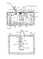
- Fig. 1 shows essential parts of an electronic apparatus including a radio IC device according to a first embodiment of the present invention.
- the electronic apparatus contains a printed wiring board 20 on which an electromagnetic coupling module 1 and other electronic components 26 such as a chip resistor and a chip capacitor, are mounted.
- the printed wiring board also includes a shielding electrode 27 therein.
- the electromagnetic coupling module 1 includes a radio IC chip 5 processing a transmitted/received signal having a predetermined frequency and a feed circuit board 10 on which the radio IC chip 5 is disposed, as shown in Fig. 2 .
- a shielding case 28 of an apparatus doubles as a radiation plate functioning as an antenna element, and is electrically continued to second wiring electrodes 21a and 21b (see Figs. 2 and 4 ) magnetically coupled to the electromagnetic coupling module 1 on the printed wiring board 20.
- the electromagnetic coupling module 1 and the radiation plate (shielding case 28) define the radio IC device.
- the radio IC chip 5 includes a clock circuit, a logic circuit, a memory circuit or the like, and stores necessary information.
- input/output terminal electrodes 6 and packaging terminal electrodes 7 are disposed, as shown in Fig. 3 .
- the input/output terminal electrodes 6 are electrically connected to electrodes 12a and 12b (see Figs. 7 and 8 ) disposed on the surface of the feed circuit board 10 through metal bumps 8.
- the packaging terminal electrodes 7 are electrically connected to electrodes 12c and 12d through metal bumps 8.
- the material of the metal bumps 8 can be Au, Ag, solder or the like.
- a protective film 9 is provided between the surface of the feed circuit board 10 and the rear surface of the radio IC chip 5 to enhance the bonding strength between the feed circuit board 10 and the radio IC chip 5 and to protect the bumps 8.
- the shielding case 28 is made of a metal and disposed so as to cover the electromagnetic coupling module 1 and the electronic components 26 on the printed wiring board 20. In addition, the shielding case functions as a radiation plate of the electromagnetic coupling module 1, as will be described below. If the case 28 is made of a nonconductive material, an electroconductive electrode film 28' is formed on the internal surface of the case 28, as indicated by oblique lines shown in Fig. 4 , and the electrode film 28' functions as the radiation plate.
- the feed circuit board 10 contains a feed circuit (including a resonance circuit having an inductance element and a matching circuit, not shown in Fig. 2 ), and is provided with external electrodes 19a and 19b from the rear surface to the sides. Also, the connection electrodes 12a and 12d (see Figs. 7 and 8 ) are formed on the surface of the feed circuit board 10. The external electrodes 19a and 19b are electromagnetically coupled to the resonance circuit contained in the feed circuit board 10 and electrically connected to the second wiring electrodes 21a and 21b with an electroconductive adhesive 29. The electrical connection may be established by soldering.
- the feed circuit board 10 contains a resonance circuit having a predetermined resonance frequency that transmits a signal having the predetermined frequency generated from the radio IC chip 5 to the shielding case 28 (or the electrode film 28') through the external electrodes 19a and 19b and the wiring electrodes 21a and 21b, and supplies a signal having the predetermined frequency selected from the signals received by the shielding case 28 (or the electrode film 28') to the radio IC chip 5.
- the radio IC chip 5 operates according to the signal received by the shielding case 28 (or the electrode film 28'), and an answer signal from the radio IC chip 5 is radiated from the shielding case 28 (or the electrode film 28').
- the external electrodes 19a and 19b disposed on the surface of the feed circuit board 10 are electromagnetically coupled to the resonance circuit contained in the feed circuit board 10 and electrically continued to the shielding case 28 functioning as an antenna.
- the electromagnetic coupling module 1 does not require a relatively large antenna element separately, and accordingly can be small. Since the feed circuit board 10 has been miniaturized, the radio IC chip 5 can be mounted on a miniaturized feed circuit board 10 by a conventionally used IC mounter or the like, and thus the packaging cost can be reduced. All that is required to change the working frequency is to modify the design of the feed circuit, and the shielding case 28 may be used without being modified.
- the shielding case 28 is relatively large and can ensure desired radiation characteristics.
- the electroconductive adhesive 29 for bonding the external electrodes 19a and 19b with the second wiring electrodes 21a and 21b contains metal particles.
- Such an adhesive 29 exhibits a small difference in thermal expansion from the external electrodes 19 and 19b and the wiring electrodes 21a and 21b when they undergo temperature changes, and accordingly the bonding reliability is enhanced.
- the second wiring electrodes 21a and 21b may be formed within the printed wiring board 20.
- the second wiring electrodes 21a and 21b are electrically connected to the electrodes on the surface of the wiring board 20 through a known via hole conductor.
- the printed wiring board 20 may be a ceramic multilayer substrate or a resin substrate.
- Fig. 5 shows essential parts of an electronic apparatus including a radio IC device according to a second embodiment of the present invention.
- the electronic apparatus contains a plurality of printed wiring boards 31 and 32 covered with a case 33.
- the printed wiring boards 31 and 32 are disposed on a substrate 30.
- One printed wiring board 31 is provided with an electromagnetic coupling module 1 and other electronic components thereon, and the other printed wiring board 32 is provided with other electronic components thereon.
- the external electrodes 19a and 19b (see Fig. 2 ) of the electromagnetic coupling module 1 are electrically connected to second wiring electrodes 21a and 21b disposed on the printed wiring board 31, as shown in Fig. 6 .
- the wiring electrodes 21a and 21b are connected to one end of a wiring cable 36 acting as a first wiring electrode provided to a known wiring connector 35.
- the other end of the wiring cable 36 is fixed to a securing member 37 disposed on the printed wiring board 32 and is electrically open.
- the wiring cable 36 between the wiring boards 31 and 32 functions as a radiation plate of the electromagnetic coupling module 1.
- an RFID system is defined, and transmits and receives high-frequency signals to and from a reader/writer.
- the same effects are produced as in the first embodiment.
- Fig. 7 shows a resonance circuit according to a first embodiment, in which the feed circuit board 10 contains the resonance circuit.
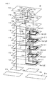
- the feed circuit board 10 is prepared by stacking dielectric ceramic sheets 11A to 11H, and pressing and firing the stack.
- the sheet 11A is provided with connection electrodes 12a and 12b, electrodes 12c and 12d, and via hole conductors 13a and 13b.
- the sheet 11B is provided with a capacitor electrode 18a, conductor patterns 15a and 15b, and via hole conductors 13c to 13e.
- the sheet 11C is provided with a capacitor electrode 18b and via hole conductors 13d to 13f.
- the sheet 11D is provided with conductor patterns 16a and 16b and via hole conductors 13e, 13f, 14a, 14b and 14d.
- the sheet 11E is provided with conductor patterns 16a and 16b and via hole conductors 13e, 13f, 14a, 14c and 14e.
- the sheet 11F is provided with a capacitor electrode 17, conductor patterns 16a and 16b and via hole conductors 13e, 13f, 14f and 14g.
- the sheet 11G is provided with conductor patterns 16a and 16b and via hole conductors 13e, 13f, 14f and 14g.
- the sheet 11H is provided with conductor patterns 16a and 16b and a via hole conductor 13f.
- a conductor pattern 16a is formed in a spiral manner continuing through the via hole conductors 14c, 14d and 14g, thus defining an inductance element L1
- a conductor pattern 16b is formed in a spiral manner continuing through the via hole conductors 14b, 14e and 14f, thus defining an inductance element L2.
- a capacitance element C1 is defined by capacitor electrodes 18a and 18b
- a capacitance element C2 is defined by capacitor electrodes 18b and 17.
- One end of the inductance element L1 is connected to the capacitor electrode 18b through the via hole conductor 13d, conductor pattern 15a and the via hole conductor 13c, and one end of the inductance element L2 is connected to the capacitor electrode 17 through the via hole conductor 14a.
- the other ends of the inductance elements L1 and L2 are brought together on the sheet 11H and connected to the connection electrode 12a through the via hole conductor 13e, the conductor pattern 15b and the via hole conductor 13a.
- the capacitor electrode 18a is electrically connected to the connection electrode 12b through the via hole conductor 13b.
- connection electrodes 12a and 12b are electrically connected to the input/output terminal electrodes 6 (see Fig. 3 ) of the radio IC chip 5 through the metal bumps 8 (see Fig. 2 ).
- the electrodes 12c and 12d are connected to the packing terminal electrodes 7 of the radio IC chip 5.
- the external electrodes 19a and 19b are formed on the rear surface of the feed circuit board 10 by applying a conductive paste.
- the external electrode 19a is coupled to the inductance elements L (L1 and L2) by a magnetic field, and the external electrode 19b is connected to the capacitor electrode 18b through the via hole conductor 13f.
- the external electrodes 19a and 19b are electrically connected to the wiring electrodes 21a and 21b, as described above.
- the inductance elements L1 and L2 are arranged in such a manner that two conductor patterns 16a and 16b are disposed in parallel.
- the two conductor patterns 16a and 16b have different line lengths from each other to have different resonance frequencies.
- the radio IC device can be used for a wide range of frequencies.
- the ceramic sheets 11A to 11H may be made of a magnetic ceramic material, and the feed circuit board 10 can be easily produced by a known process for forming a multilayer substrate, such as stacking sheets or printing into a thick film.
- the sheets 11A to 11H may be flexible sheets made of, for example, a dielectric material such as polyimide or liquid crystal polymer. Electrodes or conductors are formed on such flexible sheets by a thick film forming process, and then the sheets are stacked one on top of another and thermally compressed into a multilayer composite. Thus, the inductance elements L1 and L2 and the capacitance elements C1 and C2 may be disposed within the circuit board.
- the inductance elements L1 and L2 and the capacitance elements C1 and C2 are disposed at different positions when viewed from above.
- the inductance elements L1 and L2 are coupled to the external electrode 19a (wiring electrode 21a) by a magnetic field
- the capacitance element C1 is coupled to the external electrode 19b (wiring electrode 21b) by an electric field.
- the electromagnetic coupling module 1 including the radio IC chip 5 on the feed circuit board 10 receives high-frequency signals (for example, UHF frequencies) radiated from a reader/writer (not shown) with a shielding case 28 or a wiring cable 36, so that the resonance circuit coupled to the external electrodes 19a and 19b through the wiring electrodes 21a and 21b by a magnetic field and an electric field resonates to supply only a received signal having a predetermined frequency to the radio IC chip 5. A predetermined energy is extracted from the received signal.
- high-frequency signals for example, UHF frequencies
- the energy is used as a driving source to match the information stored in the radio IC chip 5 with a predetermined frequency by a resonance circuit, and to transmit the information to the shielding case 28 or the wiring cable 36 through the external electrodes 19a and 19b and the wiring electrodes 21a and 21b, and further transmit or transfer the information to the reader/writer from the case 28 or the cable 36.
- the resonance frequency characteristics of the feed circuit board 10 depend on the resonance circuit including the inductance elements L1 and L2 and the capacitance elements C1 and C2.
- the resonance frequency of the signal radiated from the shielding case 28 or the wiring cable 36 substantially depends on the self resonant frequency of the resonance circuit. It is accordingly not necessary to redesign the resonance circuit even if the shielding case 28 or the wiring cable 36 is changed in shape or material. Thus, the resonance circuit can be applied to various electronic apparatuses.
- the resonance circuit doubles as a matching circuit for matching the impedances between the radio IC chip 5 and the radiation plate (shielding case 28 or wiring cable 36).
- the feed circuit board 10 may include a matching circuit provided in addition to the resonance circuit including the inductance elements and the capacitance elements (in this sense, the resonance circuit may be referred to as matching circuit).
- the design for a resonance circuit doubling as a matching circuit tends to be complicated. A structure in which a matching circuit is provided apart from the resonance circuit allows the resonance circuit and the matching circuit to be designed independently.
- the resonance circuit may be replaced with a matching circuit.
- the resonance circuit may be designed in view of the shape and size of the radiation plate, or the shielding case 28 or the wiring cable 36.
- Fig. 8 shows a resonance circuit according to a second embodiment, in which the resonance circuit is disposed on a feed circuit board 40.
- This feed circuit board 40 is made of a flexible PET film or the like, and on which a spiral conductor pattern 42 defining inductance elements L and a capacitor electrode 43 defining a capacitance element C are disposed.
- Electrodes 12a and 12b extending from the conductor pattern 42 and the capacitor electrode 43 are electrically connected to the terminal electrodes 6 of the radio IC chip 5.
- Electrodes 12c and 12d formed on the circuit board 40 act as terminal ground electrodes and are electrically connected to the terminal electrodes 7 of the radio IC chip 5.
- the feed circuit board 40 is the same as that of the first embodiment in that the inductance elements L and the capacitance element C define a resonance circuit and are coupled to the respectively opposing second wiring electrodes 21a and 21b by a magnetic field and an electric field to transmit and receive a high-frequency signal having a predetermined frequency.
- the feed circuit board 40 made of a flexible film leads to a thin electromagnetic coupling module 1.
- the inductances of the inductance elements L can be varied by varying the line width or the line pitch of the conductor pattern 42, and thus the resonance frequency can be precisely adjusted.
- the conductor pattern 42 defining the inductance elements L includes two spiral lines that are connected to each other at the center of the spirals.
- the two lines of the conductor pattern 42 have respective inductances L1 and L2 and their resonance frequencies can be set to different values.
- the resulting radio IC device can be used in a wide range of frequencies as that of the first embodiment.
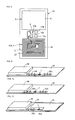
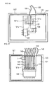
- second wiring electrodes 22a and 22b are formed in a meandering manner on the printed wiring board 20 of an electronic apparatus.
- the electromagnetic coupling module 1 is mounted on one end of each of the wiring electrodes 22a and 22b, as shown in Fig. 9 .
- a metal case 50 of a battery or liquid crystal panel is disposed close to the electrode 22b on the printed wiring board 20.
- the electromagnetic coupling module 1 is coupled to the wiring electrodes 22a and 22b in the same manner as in the first and the second embodiment.
- the second wiring electrodes 22a and 22b function as the radiation plate, and the metal case 50 by the wiring electrode 22b is coupled to the wiring electrode 22b to function as the radiation palate.
- the wiring electrodes 22a and 22b themselves can function as the radiation plate, and, in addition, the metal case 50 is also used as the radiation plate. Consequently, the radiation characteristics and the antenna gain are enhanced.
- the radio IC device of the third embodiment can function without the metal case 50. By matching the resonance frequency of the metal case 50 to the working frequency of the radio IC device, the antenna gain can further be enhanced.
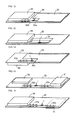
- the radio IC device has the same structure as that of the third embodiment except that part of the metal case 50 used in the third embodiment is disposed on the wiring electrode 22b, as shown in Fig. 10 .
- the fourth embodiment produces the same effects as the third embodiment. Since the metal case 50 overlaps the wiring electrode 22b, particularly the degree of their coupling is increased.
- the wiring electrode 22a is electrically connected to a ground electrode 23 disposed on the printed wiring board 20, and the other wiring electrode 22b is disposed close to the metal case 50, as shown in Fig. 11 .
- the ground electrode 23 may be contained in the printed wiring board 20.
- the wiring electrode 22a may be connected to the ground electrode 23 through a via-hole conductor, or may be formed in a meandering manner as shown in Fig. 9 and overlap the ground electrode 23.
- the wiring electrode 22b and the metal case 50 function as a radiation plate, and, in addition, the ground electrode 23 connected to the wiring electrode 22a also function as a radiation plate. Since the ground electrode 23 has a large area, the radiation characteristics and the antenna gain are enhanced.
- the radio IC device has the same structure as that of the fifth embodiment except that part of the metal case 50 used in the fifth embodiment is disposed on the wiring electrode 22b, as shown in Fig. 12 .
- the sixth embodiment produces the same effects as the fifth embodiment. Since the metal case 50 overlaps the wiring electrode 22b, particularly the degree of their coupling is increased.
- a loop electrode 24 acting as the second wiring electrode is disposed on the printed wiring board 20, and the electromagnetic coupling module 1 is disposed on both ends of the line of the loop electrode 24, as shown in Fig. 13 .
- the metal case 50 is disposed close to the loop electrode 24 on the printed wiring board 20.
- the electromagnetic coupling module 1 is coupled to the loop electrodes 24 in the same manner as in the first and the second embodiment.
- the loop electrode 24 functions as a radiation plate, and the metal case 50 coupled to the loop electrode 24 also functions as a radiation plate.
- the loop electrode 24 can match the impedances between the radio IC chip 5 and the radiation plate, and thus enhances the signal transmission efficiency between the radio IC chip 5 and the radiation plate without requiring an additional matching portion.
- the metal case 50 used in the sixth embodiment (see Fig. 12 ) is disposed on the rear surface of the printed wiring board 20, as shown in Fig. 14 . Part of the metal case 50 is coupled to the wiring electrode 22b with the printed wiring board 20 therebetween.
- the other structure is the same as in the sixth embodiment.
- the eighth embodiment produces the same effects as the sixth embodiment. Since the metal case 50 is disposed on the rear surface of the printed wiring board 20, the ground electrode 23 can be formed with a large area.
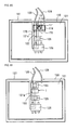
- another metal case 51 is added close to the wiring electrode 22a on the surface of the printed wiring board 20 of the third embodiment (see Fig. 9 ), as shown in Fig. 15 .
- the metal case 51 is coupled to the wiring electrode 22a to function as a radiation plate, and, thus, the antenna gain is further enhanced.
- the metal case 51 used in the ninth embodiment is disposed on the rear surface of the printed wiring board 20, as shown in Fig. 16 .
- the metal case 51 is coupled to the wiring electrode 22a with the printed wiring board 20 therebetween.
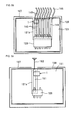
- the printed wiring board 20 is enclosed by an upper and a lower metal case 52 and 53, as shown in Figs. 17 and 18 , and the metal cases 52 and 53 function as radiation plates.
- Wiring electrodes 22a and 22b are formed on the printed wiring board 20 and coupled to the electromagnetic coupling module 1.
- the wiring electrode 22a is disposed on the rear side and connected to the front side through a via hole conductor.
- the wiring electrode 22b is disposed on the front side.
- the metal case 52 has a coupling conductor 52a to help the metal case 52 couple efficiently to the wiring electrode 22b
- the metal case 53 has a coupling conductor 53a to help the metal case 53 couple efficiently to the wiring electrode 22a.
- the wiring electrodes 22a and 22b function as radiation plates, and the metal cases 52 and 53 coupled to the respective wiring electrodes 22a and 22b also function as the radiation plates.
- the radiation characteristics and the antenna gain are enhanced.
- part of the metal case 50 is disposed on the ground electrode 23 connected to the wiring electrode 22a as shown in the fifth embodiment (see Fig. 11 ), as shown in Fig. 20 .
- the ground electrode 23 and the metal case 50 are coupled to each other to function as a radiation plate.
- the area of the loop electrode 25 provided as the second wiring electrode is increased as shown in Fig. 21 so that the loop electrode 25 can be used as a ground electrode 23 or a power supply electrode.
- the metal case 50 is disposed on part of the loop electrode 25. In the 13th embodiment, the loop electrode 25 and the metal case 50 function as a radiation plate.
- the loop electrode 25 provided as the second wiring electrode and the ground electrode 23 are integrated to function as a radiation plate, and a metal case 54 electrically connected to the ground electrode 23 is disposed on the printed wiring board 20 so as to cover the radiation plate, as shown in Fig. 22 .
- the metal case 54 has a notch 55 in a region corresponding to the loop electrode 25 when viewed from above. Since a magnetic field is generated around the loop electrode 25, the magnetic field is radiated out of the metal case 54 through the notch 55 over the loop electrode 25. Thus, the radiation characteristics are enhanced.
- the metal case 54 may be disposed so as to cover at least one of other electronic components (not shown).
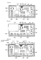
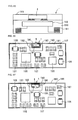
- a ground electrode 101 having an opening 102 is disposed on a printed wiring board 100, and a pair of loop electrodes 103 functioning as inductance elements are formed in the opening 102, as shown in Fig. 23 .
- the electromagnetic coupling module 1 (or radio IC chip 5 alone) is coupled to the end of each loop electrode 103.
- the printed wiring board 100 has switching modules 105, ICs 106, and other elements 107 such as chip resistors and chip capacitors thereon.
- the printed wiring board 100 is covered with a shielding case 109.
- a USB connector 110 is connected to the printed wiring board 100.
- the metal portion of the connector 110 is electrically continued to the ground electrode 101 and functions as a radiation plate of the electromagnetic coupling module 1.
- the ground electrode 101 has a slit 104 by the connector 110, so that electromagnetic waves through the connector 110 can efficiently propagate to the loop electrodes 103.
- Fig. 24 shows a state before the shielding case 109 and the connector 110 are disposed on the printed wiring board 100.
- the ground electrode 101 functions as a radiation plate.
- the structure of the 15th embodiment can function as a radio IC device from a stage shown in Fig. 24 to the final stage shown in Fig. 23 of the manufacturing process.
- the shielding wire 111a of a coaxial cable (power supply cable) 111 is electrically connected to the ground electrode 101 disposed on the printed wiring board 100, as shown in Fig. 25 .
- the other structure is the same as in the 15th embodiment.
- the shielding wire 111a of the coaxial cable 111 electrically connected to the ground electrode 101 functions as a radiation plate of the electromagnetic coupling module 1. Since the shielding wire 111a is long, communication can be performed even with weak electromagnetic waves.
- a slot case 112 of a USB card is electrically connected to the ground electrode 101 disposed on the printed wiring board 100, as shown in Fig. 26 .
- the other structure is the same as in the 15th embodiment.
- the slot case 112 is a metal component, and is electrically continued to the ground electrode 101 to function as a radiation plate of the electromagnetic coupling module 1.
- the metal case of a battery 113 is electrically connected to the ground electrode 101 disposed on the printed wiring board 100, as shown in Fig. 27 .
- the other structure is the same as in the 15th embodiment.
- the metal case of the battery 113 is electrically continued to the ground electrode 101 to function as the radiation plate of the electromagnetic coupling module 1.
- the shielding case 109 of the 15th embodiment shown in Fig. 23 is electrically connected to the ground electrode 101 through a conductor portion 109a, as shown in Fig. 28 .
- the other structure is the same as in the 15th embodiment.
- the shielding case 109 as well as the metal portion of the connector 110 functions as a radiation plate.
- the ground electrode 101 has a slit 104 by the conductor portion 109a, so that electromagnetic waves through the shielding case 109 can efficiently propagate to the loop electrode 103.
- the shielding case 109 of the 16th embodiment shown in Fig. 25 is electrically connected to the ground electrode 101 through a conductor portion 109a, as shown in Fig. 29 .
- the other structure is the same as in the 16th embodiment.
- the shielding case 109 as well as the shielding wire 111a of the coaxial cable 111 functions as a radiation plate.
- the ground electrode 101 has a slit 104 by the conductor portion 109a, so that electromagnetic waves through the shielding case 109 can efficiently propagate to the loop electrode 103.
- a ground electrode 121 disposed on a printed wiring board 120 has a slit opening 121a, as shown in Fig. 30 .
- a wiring electrode (hereinafter referred to as power line 122) is provided in the slit opening 121a.
- a power supply cable 128 is connected to the ground electrode 121, and another power supply cable 129 is connected to the power line 122.
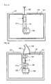
- the electromagnetic coupling module 1 is bonded on the power line 122.
- the printed wiring board 120 is covered with a shielding case 127 and the power supply cables 128 and 129 extend long out of the shielding case 127.
- the power line 122 is provided with a capacitor 125 for rejecting high-frequency noises, a voltage regulator 126 and the like to stabilize the voltage.
- the electromagnetic coupling module 1 includes a feed circuit board 130 containing a coil (inductance element) 131, a radio IC chip 5 on the feed circuit board 130, and a resin protecting member 141 covering the feed circuit board 130 and the radio IC chip 5, as shown in Fig. 32 .
- the coil 131 is disposed in such a manner that the coil axis extends parallel to the power line 122, and each end of which is electrically connected to the radio IC chip 5.
- the radio IC device of the 21st embodiment when the power supply cable 129 receives magnetic waves from a reader/writer (not shown), the power line 122 generates a current, as shown in Fig. 31 .
- the current flows to the ground electrode 121 through the capacitor 125 to generate a magnetic field ⁇ at the power line 122.
- the magnetic field ⁇ is coupled to the coil 131 of the feed circuit board 130, thus operating the radio IC chip 5.
- the power supply cable 129 functions as a radiation plate. Also, the power line 122 functions as a radiation plate in the course of the manufacturing process in which the shielding case 127 or the power supply cable 129 is not provided.
- the power supply cable 129 may be directly connected to the reader/writer.
- the feed circuit board 130 of the electromagnetic coupling module 1 is provided with a matching circuit/resonance circuit 132 in addition to the coil 131, as shown in Fig. 33 .
- the other structure is the same as in the 21st embodiment.
- the 22nd embodiment produces the same effects as the 21st embodiment.
- the circuit 132 is a matching circuit
- the matching with the coil 131 can be made, so that the radio IC chip 5 can be operated even at a low power.
- the radio IC chip can be frequency-selective, and accordingly the variation in frequency can be reduced.
- the radio IC chip can work in a wide range of frequencies.
- the feed circuit board 130 of the electromagnetic coupling module 1 is provided with a pair of external terminal electrodes 133 on the rear surface thereof, as shown in Fig. 34 .
- the other structure is the same as in the 21st embodiment.
- the 23rd embodiment produces the same effects as the 21st embodiment.
- the external terminal electrodes 133 formed on the rear surface of the feed circuit board 130 allow the electromagnetic coupling module 1 to be joined to the power line 122 with solder; hence, the electromagnetic coupling module 1 can be mounted simultaneously with other surface mount components.
- only a single external terminal electrode 133 may be formed at substantially the center of the rear surface of the feed circuit board 130.
- the feed circuit board 130 of the electromagnetic coupling module 1 is provided with a pair of external terminal electrodes 133 on the rear surface thereof, as shown in Fig. 35 .
- a conductor 134 is disposed within the feed circuit board 130 on the rear surface side, and the power line 122 is cut under the conductor 134.
- the other structure is the same as in the 21st and the 23rd embodiment.
- the 24th embodiment produces the same effects as the 21st and the 23rd embodiment. Since the current running in the power line 122 is conducted to flow near the coil 131 by the conductor 134, the degree of coupling is enhanced, and accordingly the radio IC chip can operate at a low power. In addition, the variation in coupling degree is reduced.
- an auxiliary substrate 140 is provided on which an electromagnetic coupling module 1 is mounted, as shown in Fig. 36 .
- a coupling electrode 141 having an opening 142 is formed on the auxiliary substrate 140, and a pair of loop electrodes 143 functioning as inductance elements is formed in the opening 142.
- the electromagnetic coupling module 1 (or radio IC chip 5 alone) is coupled to the end of each loop electrode 143.
- the other structure is the same as in the 21st embodiment.
- the electromagnetic coupling module 1 is coupled to the loop electrodes 143, and in addition, the coupling electrode 141 is coupled to the power line 122.
- the use of the auxiliary substrate 140 allows the use of a large coupling electrode 141 or the increase of the coil 131 in the feed circuit board 130.
- the degree of coupling to the power line 122 can be increased.
- the coupling electrode 141 on the auxiliary substrate 140 can function as the radiation plate by itself, and can be disposed anywhere on the printed wiring board 120.
- a power line 122 on which the electromagnetic coupling module 1 is mounted is formed so as to extend long in the lateral direction along an edge of the printed wiring board 120, as shown in Fig. 37 .
- the other structure is the same as in the 21st embodiment (see Fig. 30 ).
- the 26th embodiment produces the same effects as the 21st embodiment.
- the lengthened power line 122 can more function as the radiation plate and allows the radio IC device to function before the shielding case 127 or the power supply cable 129 is provided.
- the power line 122 shown in Fig. 37 is branched so as to extend long in the lateral direction along an edge of the printed wiring board 120, as shown in Fig. 38 .
- the other structure is the same as in the 21st and the 26th embodiment. Since the power line 122 functioning as a radiation plate of the 27th embodiment is longer than that of the 26th embodiment, electromagnetic waves can be more efficiently transmitted and received, and the operation can be performed at a low power.
- the power line 122 has such a length as can resonate.
- the extensions of the power line 122 shown in Fig. 38 are formed in a meandering manner, as shown in Fig. 39 .
- the other structure is the same as in the 21st embodiment.
- the power line 122 functioning as a radiation plate is substantially large, and accordingly electromagnetic waves can be transmitted and received more efficiently.
- the ground electrode 121 disposed on the printed wiring board 120 has a relatively large opening 121b in which a plurality of line electrodes 145 are formed in parallel with each other.
- the line electrodes 145 are connected to signal lines 146, such as for a USB, and one of which is coupled to the electromagnetic coupling module 1, as shown in Fig. 40 .
- a regulator 126 is disposed between the line electrodes 145 and the ground electrode 121.
- the signal lines 146 functions as a radiation plate, and the same effects are produced as in the 21st embodiment and other embodiments.
- the radio IC device can function even though it is driven by a battery and does not have a power supply cable.
- the electrode 121 disposed on the printed wiring board 120 has a slit opening 121a, as shown in Fig. 41 .
- An antenna line 151 is disposed in the slit opening 121a, and an antenna wire 152 is connected to the antenna line 151.
- the electromagnetic coupling module 1 is coupled to the antenna line 151.
- the regulator 126 is disposed between the antenna line 151 and the ground electrode 121.
- the antenna wire 152 functions as a radiation plate, and the same effects are produced as in the 21st embodiment and other embodiments.
- the electromagnetic coupling module 1 is provided with a resonance circuit or a matching circuit so that energy is transmitted to the radio IC chip 5 only at a frequency at which the IC chip 5 operates as an RFID, thus preventing the interference with the operation of the antenna.
- the antenna wire 152 intended to receive electromagnetic waves efficiently is used as a radiation plate. Accordingly, the operation can be performed at a low power.
- an anti-ESD device such as a varistor 153
- the electromagnetic coupling module 1 is disposed downstream from the varistor 153, as shown in Fig. 42 .
- the other structure is the same as in the 21st embodiment (see Fig. 30 ).
- the 31st embodiment produces the same effects as the 21st embodiment.
- the presence of the varistor 153 enhances the electrostatic surge resistance.
- the radio IC device is the same as that of the 21st embodiment (see Fig. 30 ) in that the electromagnetic coupling module 1 is coupled to the power line 122, as shown in Fig. 43 .
- the two embodiments have a difference in that the coil 131 provided on the feed circuit board 130 is disposed in such a manner that the coil axis extends in the direction perpendicular to the power line 122.
- the 32nd embodiment produces the same effects as the 21st embodiment.
- the coil 131 is formed in such a manner that the coil axis extends in the direction in which the sheets of the feed circuit board 130 are stacked, and this facilitates the formation of the coil 131.
- the ground electrode 121 disposed on the printed wiring board 120 has a slit opening 121a, as shown in Fig. 44 .
- a power line 122 is disposed in the slit opening 121a.
- a power supply cable 128 is connected to the ground electrode 121, and another power supply cable 129 is connected to the power line 122.
- an electromagnetic coupling module 1 is bonded across the region between the power line 122 and the ground electrode 121.
- the printed wiring board 120 is covered with a shielding case 127 and the power supply cables 128 and 129 extend long out of the shielding case 127.
- the power line 122 is provided with a capacitor 125 for rejecting high-frequency noises, a voltage regulator 126 and the like to stabilize the voltage.
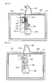
- the electromagnetic coupling module 1 includes the radio IC chip 5 and a feed circuit board 160, as shown in Fig. 45 .
- the feed circuit board 160 contains inductance elements L11 and L12 magnetically coupled to each other, and a resonance circuit having a predetermined resonance frequency with capacitors defined by an internal electrode 161 and a ground electrode 121 and by an internal electrode 162 and a power line 122.
- the radio IC chip 5 is electrically connected to the resonance circuit with solder bumps.
- reference numeral 156 designates an adhesive
- reference numeral 166 designates a protective layer for the solder bumps.
- the power line 122 when the power supply cable 129 receives magnetic waves from a reader/writer (not shown), the power line 122 generates a current.
- the power line 122 and the ground electrode 121 have a potential difference therebetween, because of the presence of an inductance component (in a coil form) as shown in Fig. 44 in view of high frequency.
- the occurrence of the potential difference allows the internal electrodes 161 and 162 of the feed circuit board 160 to be electromagnetically coupled to the ground electrode 121 and the power line 122, so that a signal operates the radio IC chip 5 through the resonance circuit.
- the power supply cable 129 functions as a radiation plate, and basically the same effects are produced as in the 21st embodiment (see Fig. 30 ). Since the feed circuit board 160 contains the resonance circuit including the inductance elements L11 and L12 and the capacitor, the feed circuit board has a function for matching with the radio IC chip 5 and a function for selecting frequency. Thus, signals can be transmitted in a wide range of frequencies.
- the electromagnetic coupling module 1 may be replaced with only a radio IC chip 5.
- the resonance circuit provided in the feed circuit board 160 of the electromagnetic coupling module 1 is defined by inductance elements L11, L12 and L13 coupled to each other, as shown in Fig. 46 .
- the other structure is the same as in the 33rd embodiment, and the same effects are produced as in the 33rd embodiment.
- the resonance circuit is bilaterally symmetrical, the electromagnetic coupling module 1 can be mounted without considering the directivity.
- external terminal electrodes 163 and 164 opposing the internal electrodes 161 and 162 are formed on the rear surface of the feed circuit board 160, as shown in Fig. 47 .
- the other structure is the same as in the 34th embodiment, and the same effects are produced as in the 34th embodiment.
- the electromagnetic coupling module 1 can be bonded on the printed wiring board 120 with solder, and thus can be mounted simultaneously with other surface mount components.
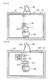
- a power line 122 on which the electromagnetic coupling module 1 is mounted is formed so as to extend long in the lateral direction along an edge of the printed wiring board 120, as shown in Fig. 48 .
- the other structure is the same as in the 33rd embodiment (see Fig. 44 ).
- the 36th embodiment produces the same effects as the 33rd embodiment.
- the lengthened power line 122 can more function as the radiation plate and allows the radio IC device to function before the shielding case 127 or the power supply cable 129 is provided.
- the extension of the power line 122 shown in Fig. 48 is formed in a meandering manner, as shown in Fig. 49 .
- the other structure is the same as in the 33rd embodiment.
- the power line 122 functioning as a radiation plate is substantially large, and accordingly electromagnetic waves can be transmitted and received more efficiently.
- the power line 122 shown in Fig. 48 is branched so as to extend long in the lateral direction along an edge of the printed wiring board 120, as shown in Fig. 50 .
- the other structure is the same as in the 33rd and the 36th embodiment. Since the power line 122 functioning as a radiation plate of the 38th embodiment is longer than that of the 36th embodiment, electromagnetic waves can be more efficiently transmitted and received, and the operation can be performed at a low power.
- the power line 122 has such a length as can resonate.
- the extensions to both sides of the power line 122 are formed in a meandering manner, as shown in Fig. 51 .
- the other structure is the same as in the 33rd embodiment.
- the power line 122 functioning as a radiation plate is substantially large, and accordingly electromagnetic waves can be transmitted and received more efficiently.
- part of the power line 122 is formed under the printed wiring board 120, as shown in Fig. 52 , and the electromagnetic coupling module 1 is mounted across the region between the power line 122 exposed at the surface and the ground electrode 121.
- the power supply cable 129 is connected to an end 122a of the power line exposed at the surface.
- the other structure is the same as in the 33rd embodiment, and the same effects are produced as in the 33rd embodiment.
- the power line 122 is partially disposed under the printed wiring board 120, the flexibility of wiring on the surface is enhanced.
- the power line 122 is bent in a C shape and both ends of the electromagnetic coupling module 1 are connected to the bent portions, as shown in Fig. 53 .
- the other structure is the same as in the 33rd embodiment, and the same effects are produced as in the 33rd embodiment.
- the electromagnetic coupling module 1 is mounted across the power line 122 from one end of the ground electrode 121 to the opposing end, as shown in Fig. 54 .
- the other structure is the same as in the 33rd embodiment, and the electromagnetic coupling module 1 is operated by a difference in potential produced on the ground electrode 121.
- the feed circuit board 160 contains a coil 167 coupled by a magnetic field ⁇ generated by the current flowing in the power line 122 in addition to the inductance elements L11 and L12, as shown in Fig. 55 .
- the coil 167 is connected in series with the inductance elements L11 and L12, and is thus operated by the current flowing in the power line 122.
- the coil 167 functions as a matching inductance element. Even if the power line cannot sufficiently receive magnetic waves, the ground electrode 121 can function as a radiation palate, and even if either element of the feed circuit is broken, the other element ensures the operation.
- part 121c of the ground electrode 121 coupled to the feed circuit of the electromagnetic coupling module 1 is formed in a loop, as shown in Fig. 56 .
- the other structure is the same as in the 33rd and the 42nd embodiment, and the same effects are produced as in the 33rd and the 42nd embodiments.
- the ground electrode 121 disposed on the printed wiring board 120 has a relatively large opening 121b in which a plurality of line electrodes 145 are formed in parallel with each other.
- the line electrodes 145 are connected to signal lines 146, such as for a USB, and the electromagnetic coupling module 1 is disposed across the region between the ground electrode 121 and one of the line electrodes 145 to be coupled to that one line electrode, as shown in Fig. 57 .
- a regulator 126 is disposed between the line electrodes 145 and the ground electrode 121.
- the signal lines 146 function as a radiation plate using the difference in potential between the line electrode 145 and the ground electrode 121, and the same effects are produced as in the 33rd and the 29th embodiment.
- the electromagnetic coupling module 1 is coupled so as to be disposed across the region between two adjacent line electrodes 145, as shown in Fig. 58 .
- the other structure is the same as in the 44th embodiment and the same effects are produced as in the 44th embodiment.
- the 45th embodiment uses the difference in potential between the two adjacent line electrodes 145.
- the ground electrode 121 disposed on the printed wiring board 120 has a slit opening 121a, as shown in Fig. 59 .
- An antenna line 151 is disposed in the slit opening 121a, and an antenna wire 152 is connected to the antenna line 151.
- the electromagnetic coupling module 1 is coupled so as to be disposed across a region between the antenna line 151 and the ground electrode 121.
- the regulator 126 is disposed between the antenna line 151 and the ground electrode 121.
- the antenna wire 152 functions as the radiation plate, and the same effects are produced as in the 33rd and the 30th embodiment.
- an auxiliary substrate 170 is provided on which the electromagnetic coupling module 1 is mounted, as shown in Fig. 60 .
- a coupling electrode 171 is formed on the auxiliary substrate 170, and a pair of loop electrodes 173 functioning as inductance elements is formed to the coupling electrode 171.
- the electromagnetic coupling module 1 (or radio IC chip 5 alone) is coupled to each end of the loop electrodes 173.
- the ends of the coupling electrode 171 are connected to the power line 122 and the ground electrode 121 with solder 175.
- the other structure is the same as in the 33rd embodiment.
- the electromagnetic coupling module 1 is coupled to the loop electrodes 173, and in addition, the coupling electrode 171 is disposed across the region between the power line 122 and the ground electrode 121 so as to be coupled to the power line 122 and the ground electrode 121.
- the same effects are produced as in the 33rd embodiment.
- the use of the auxiliary substrate 170 allows even a small electromagnetic coupling module 1 to be disposed across the region between the power line 122 and the ground electrode 121.
- an inductance element or the like may be formed on the auxiliary substrate 170 to reduce the size of the feed circuit board 160.
- the coupling electrode 171 on the auxiliary substrate 170 functions as a radiation plate by itself.
- an anti-ESD device such as a varistor 153
- a varistor 153 is disposed between the power line 122 and the ground electrode 121, and an electromagnetic coupling module 1 is disposed downstream from the varistor 153, as shown in Fig. 61 .
- the other structure is the same as in the 33rd embodiment (see Fig. 44 ).
- the 48th embodiment produces the same effects as the 33rd and the 31st embodiment.
- a ground electrode 181 disposed on a printed wiring board 180 has an opening 182 to define a loop electrode 183, and the electromagnetic coupling module 1 is mounted on the loop electrode 183, as shown in Fig. 62 .
- the electromagnetic coupling module 1 includes the radio IC chip 5 and a feed circuit board 190.
- the feed circuit board 190 contains a coil (inductance element) 191, as shown in Fig. 64 .
- the coil 191 is disposed in such a manner that the coil axis extends parallel to the loop electrode 183, and each end of the coil 191 is electrically connected to the radio IC chip 5.
- the loop electrode 183 when the ground electrode 181 receives magnetic waves from a reader/writer (not shown), the loop electrode 183 generates a current.
- the magnetic field ⁇ generated by the current is coupled to the coil 191 of the feed circuit board 190, thus operating the radio IC chip 5.
- the electromagnetic coupling module 1 is disposed in such a manner that a magnetic field ⁇ intersects only one side of the coil 191.
- a matching circuit/resonance circuit 192 may be provided within the feed circuit board 190, as shown on Fig. 65 .
- the elements 105, 106 and 107 disposed on the printed wiring board 180 are the same as in the 15th embodiment (see Fig. 23 ).
- the loop electrode 183 formed on the ground electrode 181 is bent in a C shape, and the electromagnetic coupling module 1 is mounted in such a manner that the coil 191 is disposed along the loop electrode 183, as shown in Fig. 66 .
- the other structure is the same as in the 49th embodiment.
- the 50th embodiment produces the same effects as the 49th embodiment.
- the degree of coupling between the coil 191 and the loop electrode 183 is enhanced and the energy can be efficiently transmitted.
- the electromagnetic coupling module 1 hardly protrudes from the edge of the printed wiring board 180.
- the electromagnetic coupling module 1 is disposed in a reverse orientation to that in the 49th embodiment (see Fig. 62 ) on the printed wiring board 180, as shown in Fig. 67 .
- the other structure is the same as in the 49th embodiment, and the same effects are produced as in the 49th embodiment.
- the feed circuit board 190 contains a coil 191 in such a manner that the coil axis extends perpendicular to the loop electrode 183, as shown in Fig. 68 .
- the 52nd embodiment produces the same effects as the 49th embodiment.
- the coil 191 is formed in such a manner that the coil axis extends in the direction in which the sheets of the feed circuit board 190 are stacked, and this facilitates the formation of the coil 191.
- the electromagnetic coupling module 1 is mounted at an edge of the ground electrode 181 without forming a loop electrode 183 on the ground electrode 181, as shown in Fig. 69 .
- the other structure is the same as in the 49th embodiment, and the same effects are produced as in the 49th embodiment.
- the electromagnetic coupling module 1 is operated by being coupled with a magnetic field generated by the current flowing in the edge of the ground electrode 181.
- a notch 184 is formed in the printed wiring board 180, and the ground electrode 181 has a loop electrode 183 at the edge around the notch 184, as shown in Fig. 70 .
- the other structure is the same as in the 49th embodiment, and the same effects are produced as in the 49th embodiment.
- the electromagnetic coupling module 1 is disposed in a corner of the ground electrode 181 as shown in Fig. 71 , unlike the 53rd embodiment in which the electromagnetic coupling module 1 is disposed substantially at the center of an edge of the ground electrode 181.
- the other structure is the same as in the 49th and the 53rd embodiment, and the same effects are produced as in the 49th and 53rd embodiment.
- the electromagnetic coupling module 1 can be disposed anywhere on the edge of the ground electrode 181.
- a notch may be formed in the corner of the printed wiring board 180 on which the electromagnetic coupling module 1 is disposed, as disclosed in the 54th embodiment, and the ground electrode 181 has a loop electrode at the edge around the notch.
- a coil 195 in a feed circuit board 190 forms a figure of 8, as shown in Fig. 72 , and the other structure is the same as in the 49th embodiment (see Fig. 62 ).
- the electromagnetic coupling module 1 is disposed on the printed wiring board 180 in such a manner that the magnetic flux ⁇ generated from the loop electrode 183 can pass through the loops of the coil 195 functioning as inductance elements, as shown in Fig. 73 .
- the ground electrode 181 functioning as a radiation plate and the electromagnetic coupling module 1 can be highly coupled.
- the electromagnetic coupling module 1 may include a square feed circuit board 200, as shown in Fig. 74 .
- the coil 201 functioning as an inductance element also has a square shape. This electromagnetic coupling module 1 can be applied to any embodiment of the present invention.
- a slit 185 is formed in the ground electrode 181 disposed on the printed wiring board 180, extending from the edge to the center.
- the slit 185 has an opening 185a at the end thereof, and the electromagnetic coupling module 1 is disposed over the opening 185a, as shown in Fig. 75 .
- the coil 191 formed on the feed circuit board 190 and the opening 185a have substantially the same shape in plan view.
- the surrounding of the opening 185a functions as a loop electrode to be magnetically coupled to the coil 191.
- the presence of the slit 185 helps the concentration of the current produced by the electromagnetic waves received by the ground electrode 181 around the opening 185a to generate a strong magnetic field, thus enhancing the degree of coupling.
- the slit 185 does not necessarily communicate with the edge of the ground electrode 181. If the slit 185 is to be formed according to the design of the printed wiring board 180, another slit is not necessarily formed for the electromagnetic coupling module 1.
- the feed circuit board may have a resonance circuit through which the radio IC is operated by the signal received by the radiation plate, and through which the answer signal from the radio IC is radiated from the radiation plate to the outside.
- the feed circuit board may include a matching circuit.
- the inductance element may be defined by a spiral electrode, and the spiral electrode may be coupled with a magnetic field generated at the wiring electrode on the wiring board.
- the wiring electrode and the ground electrode on the wiring board may be isolated from each other, and the feed circuit board may be disposed across a region between the wiring electrode and the ground electrode. If the case is a metal, the case can function as a radiation plate by itself. If the case is nonconductive, an electroconductive electrode film may be formed on the case and the electrode film is used as the radiation plate.
- the printed wiring board may include an electromagnetic coupling module and other electronic components, and a case doubling as the radiation plate is disposed so as to cover the high frequency device and other electronic components.
- the printed wiring board may include a second wiring electrode for coupling the feed circuit and the radiation plate.
- the impedances can be matched between the radio IC and the radiation plate without providing an additional matching portion, and the signal transmission efficiency can be enhanced between the radio IC and the radiation plate.
- the loop electrode may be formed in an auxiliary substrate disposed on the feed circuit board.
- a plurality of printed wiring boards may be used, and a high frequency device is disposed on at least one of the printed wiring boards.
- a case may be disposed so as to cover the high frequency device and at least one of other electronic components.
- the printed wiring board may include a second wiring electrode for coupling the feed circuit and the radiation plate, and a case may be disposed so as to cover all the electronic components and high frequency device mounted on the printed wiring board.
- the second wiring electrode may serve as part of the radiation plate. In this instance, the radiation characteristics can be enhanced, and the directivity can be changed depending on the arrangement of the second wiring electrode. At least part of the electronic components may serve as part of a radiation plate to enhance the radiation characteristics.
- the printed wiring board may include a ground electrode, and a second wiring electrode is electrically connected to the ground electrode.
- a ground electrode having a large area as a radiation plate, the radiation characteristics can further be enhanced.
- the second wiring electrode may be formed on the surface of or within the printed wiring board.
- the printed wiring board may be made of a resin or a ceramic.
- An external electrode coupled to the feed circuit may be formed on the surface of the feed circuit board.
- the feed circuit board may be made of a ceramic or liquid crystal polymer multilayer substrate, or a flexible substrate.
- a multilayer substrate allows an inductance element or a capacitance element to be disposed precisely within the feed circuit board, thus enhancing the flexibility in forming electrodes.
- the use of a flexible substrate facilitates the reduction of the thickness or profile of the feed circuit board.
- the radio IC may be rewritable as well as storing information of the commodity on which the radio IC device is attached, and may have other functions in addition to the function for an RFID system.
- radio IC device is not limited to the above-described embodiments, and various modifications may be made without departing from the scope of the invention.
- the radio IC chip can be mounted on the feed circuit board by any method other than using a metal bump.
- the radio IC chip and the feed circuit may be connected by electromagnetic coupling instead of electrical direct connection.
- the feed circuit board may include a radio IC.
- the electromagnetic coupling module may be used in a variety of apparatuses including household electrical appliances, such as TV set and refrigerator, without limiting to radio communication apparatuses, such as cellular phone.
- the present invention is useful to radio IC devices used in RFID systems, and is particularly advantageous in miniaturization without reducing the radiation characteristics.
Landscapes
- Engineering & Computer Science (AREA)
- Microelectronics & Electronic Packaging (AREA)
- Physics & Mathematics (AREA)
- General Physics & Mathematics (AREA)
- Theoretical Computer Science (AREA)
- Computer Hardware Design (AREA)
- Computer Networks & Wireless Communication (AREA)
- Electromagnetism (AREA)
- Details Of Aerials (AREA)
- Shielding Devices Or Components To Electric Or Magnetic Fields (AREA)
- Support Of Aerials (AREA)
- Aerials With Secondary Devices (AREA)
- Geometry (AREA)
- Health & Medical Sciences (AREA)
- Toxicology (AREA)
- Variable-Direction Aerials And Aerial Arrays (AREA)
Applications Claiming Priority (3)
| Application Number | Priority Date | Filing Date | Title |
|---|---|---|---|
| JP2007186391 | 2007-07-18 | ||
| JP2008044338 | 2008-02-26 | ||
| EP08791334.9A EP2166616B1 (fr) | 2007-07-18 | 2008-07-18 | Dispositif ci sans fil |
Related Parent Applications (2)
| Application Number | Title | Priority Date | Filing Date |
|---|---|---|---|
| EP08791334.9A Division EP2166616B1 (fr) | 2007-07-18 | 2008-07-18 | Dispositif ci sans fil |
| EP08791334.9 Division | 2008-07-18 |
Publications (2)
| Publication Number | Publication Date |
|---|---|
| EP2680193A1 true EP2680193A1 (fr) | 2014-01-01 |
| EP2680193B1 EP2680193B1 (fr) | 2015-11-18 |
Family
ID=40259749
Family Applications (3)
| Application Number | Title | Priority Date | Filing Date |
|---|---|---|---|
| EP08791334.9A Active EP2166616B1 (fr) | 2007-07-18 | 2008-07-18 | Dispositif ci sans fil |
| EP13186179.1A Active EP2680193B1 (fr) | 2007-07-18 | 2008-07-18 | Dispositif avec circuit RFID |
| EP12195562.9A Active EP2568419B1 (fr) | 2007-07-18 | 2008-07-18 | Dispositif avec circuit RFID |
Family Applications Before (1)
| Application Number | Title | Priority Date | Filing Date |
|---|---|---|---|
| EP08791334.9A Active EP2166616B1 (fr) | 2007-07-18 | 2008-07-18 | Dispositif ci sans fil |
Family Applications After (1)
| Application Number | Title | Priority Date | Filing Date |
|---|---|---|---|
| EP12195562.9A Active EP2568419B1 (fr) | 2007-07-18 | 2008-07-18 | Dispositif avec circuit RFID |
Country Status (5)
| Country | Link |
|---|---|
| US (4) | US9460376B2 (fr) |
| EP (3) | EP2166616B1 (fr) |
| JP (7) | JP5104865B2 (fr) |
| CN (2) | CN101682113B (fr) |
| WO (1) | WO2009011423A1 (fr) |
Families Citing this family (122)
| Publication number | Priority date | Publication date | Assignee | Title |
|---|---|---|---|---|
| US7519328B2 (en) | 2006-01-19 | 2009-04-14 | Murata Manufacturing Co., Ltd. | Wireless IC device and component for wireless IC device |
| US9064198B2 (en) | 2006-04-26 | 2015-06-23 | Murata Manufacturing Co., Ltd. | Electromagnetic-coupling-module-attached article |
| JP4281850B2 (ja) | 2006-06-30 | 2009-06-17 | 株式会社村田製作所 | 光ディスク |
| DE112007002024B4 (de) | 2006-09-26 | 2010-06-10 | Murata Mfg. Co., Ltd., Nagaokakyo-shi | Induktiv gekoppeltes Modul und Element mit induktiv gekoppeltem Modul |
| US8235299B2 (en) | 2007-07-04 | 2012-08-07 | Murata Manufacturing Co., Ltd. | Wireless IC device and component for wireless IC device |
| WO2008136226A1 (fr) | 2007-04-26 | 2008-11-13 | Murata Manufacturing Co., Ltd. | Dispositif à circuit intégré sans fil |
| JP4666102B2 (ja) | 2007-05-11 | 2011-04-06 | 株式会社村田製作所 | 無線icデバイス |
| WO2009008296A1 (fr) | 2007-07-09 | 2009-01-15 | Murata Manufacturing Co., Ltd. | Dispositif à circuit intégré sans fil |
| CN104540317B (zh) | 2007-07-17 | 2018-11-02 | 株式会社村田制作所 | 印制布线基板 |
| EP2086052B1 (fr) * | 2007-07-18 | 2012-05-02 | Murata Manufacturing Co. Ltd. | Dispositif à circuit intégré sans fil |
| JP5104865B2 (ja) | 2007-07-18 | 2012-12-19 | 株式会社村田製作所 | 無線icデバイス |
| EP2251934B1 (fr) | 2008-03-03 | 2018-05-02 | Murata Manufacturing Co. Ltd. | Dispositif à ci sans fil et système de communication sans fil |
| CN103295056B (zh) | 2008-05-21 | 2016-12-28 | 株式会社村田制作所 | 无线ic器件 |
| CN104077622B (zh) | 2008-05-26 | 2016-07-06 | 株式会社村田制作所 | 无线ic器件系统及无线ic器件的真伪判定方法 |
| WO2010021217A1 (fr) | 2008-08-19 | 2010-02-25 | 株式会社村田製作所 | Dispositif à circuit intégré sans fil et procédé de fabrication de celui-ci |
| DE112009002399B4 (de) * | 2008-10-29 | 2022-08-18 | Murata Manufacturing Co., Ltd. | Funk-IC-Bauelement |
| DE112009002384B4 (de) | 2008-11-17 | 2021-05-06 | Murata Manufacturing Co., Ltd. | Antenne und Drahtlose-IC-Bauelement |
| CN102273012B (zh) | 2009-01-09 | 2013-11-20 | 株式会社村田制作所 | 无线ic器件及无线ic模块 |
| EP2385580B1 (fr) | 2009-01-30 | 2014-04-09 | Murata Manufacturing Co., Ltd. | Antenne et dispositif de circuit intégré sans fil |
| JP5510450B2 (ja) * | 2009-04-14 | 2014-06-04 | 株式会社村田製作所 | 無線icデバイス |
| EP2424041B1 (fr) | 2009-04-21 | 2018-11-21 | Murata Manufacturing Co., Ltd. | Appareil d'antenne et procédé de réglage de la fréquence de résonance de celui-ci |
| WO2010140429A1 (fr) | 2009-06-03 | 2010-12-09 | 株式会社村田製作所 | Dispositif de circuit intégré sans fil et son procédé de production |
| JP5516580B2 (ja) | 2009-06-19 | 2014-06-11 | 株式会社村田製作所 | 無線icデバイス及び給電回路と放射板との結合方法 |
| WO2011001709A1 (fr) | 2009-07-03 | 2011-01-06 | 株式会社村田製作所 | Antenne et module d'antenne |
| JP5286195B2 (ja) * | 2009-08-18 | 2013-09-11 | トッパン・フォームズ株式会社 | 非接触通信部内蔵型金属製筐体 |
| JP5291571B2 (ja) * | 2009-08-18 | 2013-09-18 | トッパン・フォームズ株式会社 | 非接触通信部内蔵型金属製筐体 |
| JP5291570B2 (ja) * | 2009-08-18 | 2013-09-18 | トッパン・フォームズ株式会社 | 非接触通信部内蔵型金属製筐体 |
| JP5182431B2 (ja) | 2009-09-28 | 2013-04-17 | 株式会社村田製作所 | 無線icデバイスおよびそれを用いた環境状態検出方法 |
| CN102577646B (zh) | 2009-09-30 | 2015-03-04 | 株式会社村田制作所 | 电路基板及其制造方法 |
| JP5304580B2 (ja) | 2009-10-02 | 2013-10-02 | 株式会社村田製作所 | 無線icデバイス |
| CN102576939B (zh) | 2009-10-16 | 2015-11-25 | 株式会社村田制作所 | 天线及无线ic器件 |
| JP5418600B2 (ja) | 2009-10-27 | 2014-02-19 | 株式会社村田製作所 | 送受信装置及び無線タグ読み取り装置 |
| JP5327334B2 (ja) | 2009-11-04 | 2013-10-30 | 株式会社村田製作所 | 通信端末及び情報処理システム |
| CN102576930A (zh) | 2009-11-04 | 2012-07-11 | 株式会社村田制作所 | 通信终端及信息处理系统 |
| WO2011055702A1 (fr) | 2009-11-04 | 2011-05-12 | 株式会社村田製作所 | Étiquette à circuit radio intégré, lecteur/enregistreur, et système de traitement d'information |
| GB2487491B (en) | 2009-11-20 | 2014-09-03 | Murata Manufacturing Co | Antenna device and mobile communication terminal |
| JP4978756B2 (ja) | 2009-12-24 | 2012-07-18 | 株式会社村田製作所 | 通信端末 |
| WO2011093438A1 (fr) * | 2010-01-29 | 2011-08-04 | 株式会社村田製作所 | Dispositif de réception d'énergie électrique et dispositif d'émission d'énergie électrique |
| GB2477358A (en) | 2010-02-02 | 2011-08-03 | Thales Holdings Uk Plc | RF testing an integrated circuit assembly during manufacture using a interposed adaptor layer which is removed after test to attach the IC to a BGA |
| US8576561B2 (en) * | 2010-02-02 | 2013-11-05 | Apple Inc. | Handheld device enclosure |
| WO2011099973A1 (fr) * | 2010-02-11 | 2011-08-18 | Soundcraft, Inc. | Étiquette d'identification radiofréquence renforcée |
| GB2490268A (en) * | 2010-02-19 | 2012-10-24 | Murata Manufacturing Co | Composite printed wiring board and wireless communication system |
| JP5652470B2 (ja) | 2010-03-03 | 2015-01-14 | 株式会社村田製作所 | 無線通信モジュール及び無線通信デバイス |
| WO2011108341A1 (fr) | 2010-03-03 | 2011-09-09 | 株式会社村田製作所 | Dispositif de radiocommunication et terminal de radiocommunication |
| CN102576940B (zh) | 2010-03-12 | 2016-05-04 | 株式会社村田制作所 | 无线通信器件及金属制物品 |
| JP5018918B2 (ja) * | 2010-03-17 | 2012-09-05 | パナソニック株式会社 | アンテナ装置およびそれを用いた携帯端末装置 |
| CN102668241B (zh) | 2010-03-24 | 2015-01-28 | 株式会社村田制作所 | Rfid系统 |
| JP5630499B2 (ja) | 2010-03-31 | 2014-11-26 | 株式会社村田製作所 | アンテナ装置及び無線通信デバイス |
| CN102238808B (zh) * | 2010-04-22 | 2016-01-20 | 鸿富锦精密工业(深圳)有限公司 | 胶纸粘贴方法和利用该方法粘贴形成的主板 |
| JP5333366B2 (ja) * | 2010-07-07 | 2013-11-06 | オムロン株式会社 | ネットワーク機器および通信モジュール |
| JP5376060B2 (ja) | 2010-07-08 | 2013-12-25 | 株式会社村田製作所 | アンテナ及びrfidデバイス |
| GB2495418B (en) * | 2010-07-28 | 2017-05-24 | Murata Manufacturing Co | Antenna apparatus and communication terminal instrument |
| WO2012020748A1 (fr) | 2010-08-10 | 2012-02-16 | 株式会社村田製作所 | Carte de circuit imprimé et système de communication sans fil |
| CN103038939B (zh) | 2010-09-30 | 2015-11-25 | 株式会社村田制作所 | 无线ic器件 |
| CN105226382B (zh) | 2010-10-12 | 2019-06-11 | 株式会社村田制作所 | 天线装置及终端装置 |
| GB2501385B (en) | 2010-10-21 | 2015-05-27 | Murata Manufacturing Co | Communication terminal device |
| CN103026370A (zh) * | 2010-12-01 | 2013-04-03 | 株式会社村田制作所 | 电气产品 |
| CN105048058B (zh) | 2011-01-05 | 2017-10-27 | 株式会社村田制作所 | 无线通信器件 |
| JP5304956B2 (ja) | 2011-01-14 | 2013-10-02 | 株式会社村田製作所 | Rfidチップパッケージ及びrfidタグ |
| CN104899639B (zh) | 2011-02-28 | 2018-08-07 | 株式会社村田制作所 | 无线通信器件 |
| JP5630566B2 (ja) | 2011-03-08 | 2014-11-26 | 株式会社村田製作所 | アンテナ装置及び通信端末機器 |
| JP5273326B2 (ja) | 2011-04-05 | 2013-08-28 | 株式会社村田製作所 | 無線通信デバイス |
| WO2012141070A1 (fr) | 2011-04-13 | 2012-10-18 | 株式会社村田製作所 | Dispositif à circuit intégré sans fil et terminal de communication sans fil |
| WO2012157596A1 (fr) | 2011-05-16 | 2012-11-22 | 株式会社村田製作所 | Dispositif à ic sans fil |
| US9147145B2 (en) | 2011-05-31 | 2015-09-29 | United Technologies Corporation | RFID tag system |
| US8899488B2 (en) | 2011-05-31 | 2014-12-02 | United Technologies Corporation | RFID tag system |
| WO2013008874A1 (fr) | 2011-07-14 | 2013-01-17 | 株式会社村田製作所 | Dispositif de communication sans fil |
| JP5333707B2 (ja) | 2011-07-15 | 2013-11-06 | 株式会社村田製作所 | 無線通信デバイス |
| WO2013011865A1 (fr) | 2011-07-19 | 2013-01-24 | 株式会社村田製作所 | Module d'antenne, dispositif d'antenne, étiquette rfid et dispositif terminal de communication |
| JP5338875B2 (ja) * | 2011-08-25 | 2013-11-13 | 株式会社村田製作所 | Dc−dcコンバータ |
| US8941550B2 (en) * | 2011-09-09 | 2015-01-27 | Blackberry Limited | Mobile wireless communications device including a slot antenna and related methods |
| JP5418737B2 (ja) | 2011-09-09 | 2014-02-19 | 株式会社村田製作所 | アンテナ装置および無線デバイス |
| DE102012101606B4 (de) * | 2011-10-28 | 2024-11-21 | Tdk Electronics Ag | ESD-Schutzbauelement und Bauelement mit einem ESD-Schutzbauelement und einer LED |
| DE102011087588A1 (de) * | 2011-12-01 | 2013-06-06 | Endress + Hauser Conducta Gesellschaft für Mess- und Regeltechnik mbH + Co. KG | Feldgerät für die Automatisierungstechnik |
| CN103380432B (zh) | 2011-12-01 | 2016-10-19 | 株式会社村田制作所 | 无线ic器件及其制造方法 |
| JP5354137B1 (ja) | 2012-01-30 | 2013-11-27 | 株式会社村田製作所 | 無線icデバイス |
| WO2013125610A1 (fr) | 2012-02-24 | 2013-08-29 | 株式会社村田製作所 | Dispositif d'antenne et dispositif de communication sans fil |
| WO2013153697A1 (fr) | 2012-04-13 | 2013-10-17 | 株式会社村田製作所 | Procédé d'inspection d'étiquette d'identification par radiofréquence (rfid) et dispositif d'inspection |
| JP5664823B2 (ja) * | 2012-10-26 | 2015-02-04 | 株式会社村田製作所 | 通信端末及びプログラム |
| EP2937937B1 (fr) * | 2012-12-21 | 2020-01-08 | Murata Manufacturing Co., Ltd. | Dispositif d'antenne et dispositif électronique |
| JP2014179543A (ja) * | 2013-03-15 | 2014-09-25 | Hosiden Corp | 非接触給電装置および非接触受電装置 |
| US10015916B1 (en) * | 2013-05-21 | 2018-07-03 | Xilinx, Inc. | Removal of electrostatic charges from an interposer via a ground pad thereof for die attach for formation of a stacked die |
| US9583821B2 (en) * | 2013-09-04 | 2017-02-28 | Apple Inc. | Antenna related features of a mobile phone or computing device |
| US9960227B2 (en) | 2013-09-11 | 2018-05-01 | Xilinx, Inc. | Removal of electrostatic charges from interposer for die attachment |
| US9761945B2 (en) * | 2013-10-18 | 2017-09-12 | Taoglas Group Holdings Limited | Ultra-low profile monopole antenna for 2.4GHz band |
| JP6007448B2 (ja) * | 2014-01-23 | 2016-10-12 | 株式会社村田製作所 | 無線通信タグ付き物品および無線通信タグ |
| CN106471673B (zh) * | 2014-07-02 | 2019-04-23 | 株式会社村田制作所 | 天线装置、天线模块以及通信终端装置 |
| US9582750B2 (en) * | 2014-12-22 | 2017-02-28 | Avery Dennison Retail Information Services, Llc | RFID devices with multi-frequency antennae |
| US10218053B2 (en) * | 2015-09-15 | 2019-02-26 | Htc Corporation | Antenna device |
| US9825597B2 (en) | 2015-12-30 | 2017-11-21 | Skyworks Solutions, Inc. | Impedance transformation circuit for amplifier |
| JP6593202B2 (ja) * | 2016-01-29 | 2019-10-23 | セイコーエプソン株式会社 | 電子部品および腕時計 |
| US10062670B2 (en) | 2016-04-18 | 2018-08-28 | Skyworks Solutions, Inc. | Radio frequency system-in-package with stacked clocking crystal |
| KR102629723B1 (ko) | 2016-04-19 | 2024-01-30 | 스카이워크스 솔루션즈, 인코포레이티드 | 무선 주파수 모듈의 선택적 차폐 |
| US9999121B2 (en) * | 2016-04-25 | 2018-06-12 | Laird Technologies, Inc. | Board level shields with virtual grounding capability |
| US10297913B2 (en) | 2016-05-04 | 2019-05-21 | Skyworks Solutions, Inc. | Shielded radio frequency component with integrated antenna |
| JP6500859B2 (ja) * | 2016-08-22 | 2019-04-17 | 株式会社村田製作所 | 無線モジュール |
| JP2017045469A (ja) * | 2016-11-07 | 2017-03-02 | 富士通コンポーネント株式会社 | メモリカード |
| JP2018081422A (ja) * | 2016-11-15 | 2018-05-24 | 大日本印刷株式会社 | 情報記録媒体、装着体、補助アンテナ |
| JP6408540B2 (ja) * | 2016-12-01 | 2018-10-17 | 太陽誘電株式会社 | 無線モジュール及び無線モジュールの製造方法 |
| JP6449837B2 (ja) * | 2016-12-01 | 2019-01-09 | 太陽誘電株式会社 | 無線モジュール及び無線モジュールの製造方法 |
| KR102364013B1 (ko) * | 2016-12-07 | 2022-02-16 | 웨이퍼 엘엘씨 | 저손실 전기 전송 메커니즘과 이를 이용한 안테나 |
| WO2018123698A1 (fr) * | 2016-12-27 | 2018-07-05 | 株式会社村田製作所 | Module haute fréquence et dispositif de communication |
| TWI907080B (zh) | 2016-12-29 | 2025-12-01 | 美商天工方案公司 | 封裝模組、無線通信裝置及射頻信號傳輸方法 |
| JP6683289B2 (ja) * | 2017-02-28 | 2020-04-15 | 株式会社村田製作所 | 薄膜シールド層付き電子部品 |
| US10515924B2 (en) | 2017-03-10 | 2019-12-24 | Skyworks Solutions, Inc. | Radio frequency modules |
| WO2018173666A1 (fr) * | 2017-03-22 | 2018-09-27 | 株式会社村田製作所 | Substrat multicouche |
| JP6888999B2 (ja) * | 2017-03-28 | 2021-06-18 | 京セラ株式会社 | Rfid用基板およびrfidタグ |
| JP6555501B1 (ja) * | 2017-09-05 | 2019-08-07 | 株式会社村田製作所 | 電子モジュール |
| GB2567812A (en) * | 2017-10-19 | 2019-05-01 | Raspberry Pi Trading Ltd | Radio module |
| WO2019159745A1 (fr) * | 2018-02-16 | 2019-08-22 | 株式会社村田製作所 | Dispositif d'antenne et équipement électronique |
| DE102018105383B4 (de) | 2018-03-08 | 2021-12-30 | Infineon Technologies Ag | Antennenmodul, Antennenvorrichtung und Verfahren zum Herstellen eines Antennenmoduls |
| JP7077796B2 (ja) * | 2018-06-07 | 2022-05-31 | 大日本印刷株式会社 | Rfタグ構造体 |
| WO2020066086A1 (fr) * | 2018-09-25 | 2020-04-02 | 株式会社村田製作所 | Module de circuit de réception d'énergie sans fil |
| CN110113871B (zh) * | 2019-05-05 | 2020-07-07 | Oppo广东移动通信有限公司 | 电路板组件及电子设备 |
| JP7310496B2 (ja) * | 2019-09-26 | 2023-07-19 | 住友大阪セメント株式会社 | 光変調器及びそれを用いた光送信装置 |
| US11333686B2 (en) * | 2019-10-21 | 2022-05-17 | Tegam, Inc. | Non-directional in-line suspended PCB power sensing coupler |
| JP7315104B2 (ja) * | 2020-07-03 | 2023-07-26 | 株式会社村田製作所 | アンテナ装置及び電子機器 |
| JP2022040623A (ja) * | 2020-08-31 | 2022-03-11 | 日東電工株式会社 | 配線回路基板 |
| CN113346239B (zh) * | 2021-04-28 | 2022-07-26 | 荣耀终端有限公司 | 电子设备及通信系统 |
| CN117677029A (zh) * | 2022-08-31 | 2024-03-08 | 华为技术有限公司 | 信号传输结构及制作方法 |
| CN116683157B (zh) * | 2023-08-02 | 2023-10-13 | 上海博应信息技术有限公司 | 基于模块化的小型柔性抗金属标签天线 |
| WO2026038398A1 (fr) * | 2024-08-13 | 2026-02-19 | アルプスアルパイン株式会社 | Module de communication sans fil |
Citations (5)
| Publication number | Priority date | Publication date | Assignee | Title |
|---|---|---|---|---|
| JP2002232221A (ja) | 2001-01-30 | 2002-08-16 | Alps Electric Co Ltd | 送受信ユニット |
| US20060043198A1 (en) * | 2004-09-01 | 2006-03-02 | Forster Ian J | RFID device with combined reactive coupler |
| WO2007125683A1 (fr) * | 2006-04-26 | 2007-11-08 | Murata Manufacturing Co., Ltd. | Article ayant un module couple de maniere electromagnetique |
| WO2008007606A1 (fr) * | 2006-07-11 | 2008-01-17 | Murata Manufacturing Co., Ltd. | Dispositif à antenne et circuit résonnant |
| EP2264831A1 (fr) * | 2008-04-14 | 2010-12-22 | Murata Manufacturing Co. Ltd. | Dispositif de circuit intégré radio, dispositif électronique et procédé d'ajustement de fréquence de résonance de dispositif de circuit intégré radio |
Family Cites Families (579)
| Publication number | Priority date | Publication date | Assignee | Title |
|---|---|---|---|---|
| US3364564A (en) | 1965-06-28 | 1968-01-23 | Gregory Ind Inc | Method of producing welding studs dischargeable in end-to-end relationship |
| JPS5754964B2 (fr) | 1974-05-08 | 1982-11-20 | ||
| JPS5188145U (fr) | 1975-01-10 | 1976-07-14 | ||
| JPS6193701A (ja) | 1984-10-13 | 1986-05-12 | Toyota Motor Corp | 自動車用アンテナ装置 |
| JPS61123303A (ja) | 1984-11-20 | 1986-06-11 | Matsushita Electric Ind Co Ltd | 小形無線機のアンテナ |
| JPS61284102A (ja) | 1985-06-11 | 1986-12-15 | Oki Electric Ind Co Ltd | 携帯形無線機のアンテナ |
| JPS62127140U (fr) | 1986-02-03 | 1987-08-12 | ||
| US4737789A (en) * | 1986-12-02 | 1988-04-12 | X Cyte, Inc. | Inductive antenna coupling for a surface acoustic wave transponder |
| NL8700369A (nl) * | 1987-02-16 | 1988-09-16 | Nedap Nv | Werkwijze voor het plaatsen van een elektronische responder in een omgeving van metaal. |
| JPH01212035A (ja) | 1987-08-13 | 1989-08-25 | Secom Co Ltd | 電磁界ダイバ−シチ受信方式 |
| ZA89872B (en) | 1988-02-04 | 1990-10-31 | Uniscan Ltd | Concentrator |
| JPH0744114B2 (ja) | 1988-12-16 | 1995-05-15 | 株式会社村田製作所 | 積層チップコイル |
| JPH02164105A (ja) | 1988-12-19 | 1990-06-25 | Mitsubishi Electric Corp | スパイラルアンテナ |
| US5253969A (en) | 1989-03-10 | 1993-10-19 | Sms Schloemann-Siemag Aktiengesellschaft | Feeding system for strip material, particularly in treatment plants for metal strips |
| JPH03171385A (ja) | 1989-11-30 | 1991-07-24 | Sony Corp | 情報カード |
| JP2662742B2 (ja) | 1990-03-13 | 1997-10-15 | 株式会社村田製作所 | バンドパスフィルタ |
| JP2763664B2 (ja) | 1990-07-25 | 1998-06-11 | 日本碍子株式会社 | 分布定数回路用配線基板 |
| JPH04150011A (ja) | 1990-10-12 | 1992-05-22 | Tdk Corp | 複合電子部品 |
| JPH04167500A (ja) | 1990-10-30 | 1992-06-15 | Omron Corp | プリント基板管理システム |
| JP2539367Y2 (ja) | 1991-01-30 | 1997-06-25 | 株式会社村田製作所 | 積層型電子部品 |
| NL9100176A (nl) | 1991-02-01 | 1992-03-02 | Nedap Nv | Antenne met transformator voor contactloze informatieoverdracht vanuit integrated circuit-kaart. |
| JP2558330Y2 (ja) | 1991-02-06 | 1997-12-24 | オムロン株式会社 | 電磁結合型電子機器 |
| NL9100347A (nl) | 1991-02-26 | 1992-03-02 | Nedap Nv | Geintegreerde transformator voor een contactloze identificatiekaart. |
| JPH04321190A (ja) | 1991-04-22 | 1992-11-11 | Mitsubishi Electric Corp | 非接触型携帯記憶装置のアンテナ回路 |
| JPH0745933Y2 (ja) | 1991-06-07 | 1995-10-18 | 太陽誘電株式会社 | 積層セラミックインダクタンス素子 |
| DE69215283T2 (de) | 1991-07-08 | 1997-03-20 | Nippon Telegraph & Telephone | Ausfahrbares Antennensystem |
| JP2839782B2 (ja) | 1992-02-14 | 1998-12-16 | 三菱電機株式会社 | プリント化スロットアンテナ |
| JPH0591013U (ja) | 1992-05-11 | 1993-12-10 | セイコー電子工業株式会社 | 小型無線機用アンテナ |
| JPH05327331A (ja) | 1992-05-15 | 1993-12-10 | Matsushita Electric Works Ltd | プリントアンテナ |
| US5444452A (en) * | 1992-07-13 | 1995-08-22 | Matsushita Electric Works, Ltd. | Dual frequency antenna |
| JP3186235B2 (ja) | 1992-07-30 | 2001-07-11 | 株式会社村田製作所 | 共振器アンテナ |
| JPH0677729A (ja) | 1992-08-25 | 1994-03-18 | Mitsubishi Electric Corp | アンテナ一体化マイクロ波回路 |
| JP2592328Y2 (ja) | 1992-09-09 | 1999-03-17 | 神鋼電機株式会社 | アンテナ装置 |
| JPH06177635A (ja) | 1992-12-07 | 1994-06-24 | Mitsubishi Electric Corp | クロスダイポールアンテナ装置 |
| JPH06260949A (ja) * | 1993-03-03 | 1994-09-16 | Seiko Instr Inc | 無線機器 |
| US5430441A (en) * | 1993-10-12 | 1995-07-04 | Motorola, Inc. | Transponding tag and method |
| JPH07183836A (ja) | 1993-12-22 | 1995-07-21 | San'eisha Mfg Co Ltd | 配電線搬送通信用結合フィルタ装置 |
| US5491483A (en) | 1994-01-05 | 1996-02-13 | Texas Instruments Incorporated | Single loop transponder system and method |
| JPH07221529A (ja) | 1994-01-27 | 1995-08-18 | Sony Corp | アンテナ装置 |
| JPH07321688A (ja) | 1994-05-25 | 1995-12-08 | Funai Denki Kenkyusho:Kk | 無線装置の内蔵アンテナ |
| US6096431A (en) | 1994-07-25 | 2000-08-01 | Toppan Printing Co., Ltd. | Biodegradable cards |
| JP3427527B2 (ja) | 1994-12-26 | 2003-07-22 | 凸版印刷株式会社 | 生分解性積層体及び生分解性カード |
| JP2999374B2 (ja) | 1994-08-10 | 2000-01-17 | 太陽誘電株式会社 | 積層チップインダクタ |
| JP3141692B2 (ja) | 1994-08-11 | 2001-03-05 | 松下電器産業株式会社 | ミリ波用検波器 |
| DE4431754C1 (de) | 1994-09-06 | 1995-11-23 | Siemens Ag | Trägerelement |
| US5528222A (en) | 1994-09-09 | 1996-06-18 | International Business Machines Corporation | Radio frequency circuit and memory in thin flexible package |
| JPH0887580A (ja) | 1994-09-14 | 1996-04-02 | Omron Corp | データキャリア及びボールゲーム |
| JP3064840B2 (ja) | 1994-12-22 | 2000-07-12 | ソニー株式会社 | Icカード |
| JP3369019B2 (ja) | 1995-01-31 | 2003-01-20 | セイコーインスツルメンツ株式会社 | 携帯電話機用アンテナ |
| JP2837829B2 (ja) | 1995-03-31 | 1998-12-16 | 松下電器産業株式会社 | 半導体装置の検査方法 |
| JPH08279027A (ja) | 1995-04-04 | 1996-10-22 | Toshiba Corp | 無線通信カード |
| US5955723A (en) | 1995-05-03 | 1999-09-21 | Siemens Aktiengesellschaft | Contactless chip card |
| JPH08307126A (ja) | 1995-05-09 | 1996-11-22 | Kyocera Corp | アンテナの収納構造 |
| JP3637982B2 (ja) | 1995-06-27 | 2005-04-13 | 株式会社荏原電産 | インバータ駆動ポンプの制御システム |
| US5629241A (en) | 1995-07-07 | 1997-05-13 | Hughes Aircraft Company | Microwave/millimeter wave circuit structure with discrete flip-chip mounted elements, and method of fabricating the same |
| JP3150575B2 (ja) | 1995-07-18 | 2001-03-26 | 沖電気工業株式会社 | タグ装置及びその製造方法 |
| GB2305075A (en) | 1995-09-05 | 1997-03-26 | Ibm | Radio Frequency Tag for Electronic Apparatus |
| DE19534229A1 (de) | 1995-09-15 | 1997-03-20 | Licentia Gmbh | Transponderanordnung |
| JPH0993029A (ja) * | 1995-09-21 | 1997-04-04 | Matsushita Electric Ind Co Ltd | アンテナ装置 |
| US6104611A (en) | 1995-10-05 | 2000-08-15 | Nortel Networks Corporation | Packaging system for thermally controlling the temperature of electronic equipment |
| JPH09232854A (ja) | 1996-02-20 | 1997-09-05 | Matsushita Electric Ind Co Ltd | 移動無線機用小型平面アンテナ装置 |
| JP3882218B2 (ja) | 1996-03-04 | 2007-02-14 | ソニー株式会社 | 光ディスク |
| JP3471160B2 (ja) | 1996-03-18 | 2003-11-25 | 株式会社東芝 | モノリシックアンテナ |
| JPH09270623A (ja) | 1996-03-29 | 1997-10-14 | Murata Mfg Co Ltd | アンテナ装置 |
| JPH09284038A (ja) | 1996-04-17 | 1997-10-31 | Nhk Spring Co Ltd | 非接触データキャリアのアンテナ装置 |
| JPH09294374A (ja) | 1996-04-26 | 1997-11-11 | Hitachi Ltd | 電源回路 |
| JP3427663B2 (ja) | 1996-06-18 | 2003-07-22 | 凸版印刷株式会社 | 非接触icカード |
| AUPO055296A0 (en) | 1996-06-19 | 1996-07-11 | Integrated Silicon Design Pty Ltd | Enhanced range transponder system |
| US6104311A (en) | 1996-08-26 | 2000-08-15 | Addison Technologies | Information storage and identification tag |
| JP3767030B2 (ja) | 1996-09-09 | 2006-04-19 | 三菱電機株式会社 | 折畳式無線通信装置 |
| JP3392016B2 (ja) | 1996-09-13 | 2003-03-31 | 株式会社日立製作所 | 電力伝送システム並びに電力伝送および情報通信システム |
| ATE210864T1 (de) | 1996-10-09 | 2001-12-15 | Pav Card Gmbh | Verfahren und verbindungsanordnung zum herstellen einer chipkarte |
| JPH10171954A (ja) | 1996-12-05 | 1998-06-26 | Hitachi Maxell Ltd | 非接触式icカード |
| JP3279205B2 (ja) | 1996-12-10 | 2002-04-30 | 株式会社村田製作所 | 表面実装型アンテナおよび通信機 |
| JPH10193849A (ja) | 1996-12-27 | 1998-07-28 | Rohm Co Ltd | 回路チップ搭載カードおよび回路チップモジュール |
| JPH10193851A (ja) | 1997-01-08 | 1998-07-28 | Denso Corp | 非接触カード |
| DE19703029A1 (de) | 1997-01-28 | 1998-07-30 | Amatech Gmbh & Co Kg | Übertragungsmodul für eine Transpondervorrichtung sowie Transpondervorrichtung und Verfahren zum Betrieb einer Transpondervorrichtung |
| JPH10242742A (ja) | 1997-02-26 | 1998-09-11 | Harada Ind Co Ltd | 送受信アンテナ |
| US6181287B1 (en) | 1997-03-10 | 2001-01-30 | Precision Dynamics Corporation | Reactively coupled elements in circuits on flexible substrates |
| JPH10293828A (ja) | 1997-04-18 | 1998-11-04 | Omron Corp | データキャリア、コイルモジュール、リーダライタ及び衣服データ取得方法 |
| JP3900593B2 (ja) | 1997-05-27 | 2007-04-04 | 凸版印刷株式会社 | Icカードおよびicモジュール |
| JPH11346114A (ja) | 1997-06-11 | 1999-12-14 | Matsushita Electric Ind Co Ltd | アンテナ装置 |
| JPH1125244A (ja) | 1997-06-27 | 1999-01-29 | Toshiba Chem Corp | 非接触データキャリアパッケージ |
| JP3621560B2 (ja) | 1997-07-24 | 2005-02-16 | 三菱電機株式会社 | 電磁誘導型データキャリアシステム |
| JPH1175329A (ja) | 1997-08-29 | 1999-03-16 | Hitachi Ltd | 非接触icカードシステム |
| JPH1185937A (ja) | 1997-09-02 | 1999-03-30 | Nippon Lsi Card Kk | 非接触式lsiカード及びその検査方法 |
| JPH1188241A (ja) | 1997-09-04 | 1999-03-30 | Nippon Steel Corp | データキャリアシステム |
| JPH11103209A (ja) | 1997-09-26 | 1999-04-13 | Fujitsu Ten Ltd | 電波受信装置 |
| JP3853930B2 (ja) | 1997-09-26 | 2006-12-06 | 株式会社マースエンジニアリング | 非接触データキャリアパッケージおよびその製造方法 |
| JP3037226B2 (ja) | 1997-09-30 | 2000-04-24 | 静岡日本電気株式会社 | 携帯無線機のアンテナ装置 |
| JPH11149536A (ja) | 1997-11-14 | 1999-06-02 | Toppan Printing Co Ltd | 複合icカード |
| JP3800766B2 (ja) | 1997-11-14 | 2006-07-26 | 凸版印刷株式会社 | 複合icモジュールおよび複合icカード |
| WO1999026195A1 (fr) | 1997-11-14 | 1999-05-27 | Toppan Printing Co., Ltd. | Module ci composite et carte ci composite |
| JP3800765B2 (ja) | 1997-11-14 | 2006-07-26 | 凸版印刷株式会社 | 複合icカード |
| JPH11175678A (ja) | 1997-12-09 | 1999-07-02 | Toppan Printing Co Ltd | Icモジュールとそのモジュールを搭載したicカード |
| JPH11220319A (ja) | 1998-01-30 | 1999-08-10 | Sharp Corp | アンテナ装置 |
| JPH11219420A (ja) | 1998-02-03 | 1999-08-10 | Tokin Corp | Icカードモジュール、icカード及びそれらの製造方法 |
| JP2001084463A (ja) | 1999-09-14 | 2001-03-30 | Miyake:Kk | 共振回路 |
| JPH11261325A (ja) | 1998-03-10 | 1999-09-24 | Shiro Sugimura | コイル素子と、その製造方法 |
| JP4260917B2 (ja) | 1998-03-31 | 2009-04-30 | 株式会社東芝 | ループアンテナ |
| EP0987789A4 (fr) | 1998-03-31 | 2004-09-22 | Matsushita Electric Industrial Co Ltd | Antenne et televiseur numerique |
| US5936150A (en) | 1998-04-13 | 1999-08-10 | Rockwell Science Center, Llc | Thin film resonant chemical sensor with resonant acoustic isolator |
| CN1267267A (zh) | 1998-04-14 | 2000-09-20 | 德克萨斯黎伯迪纸板箱公司 | 用于压缩机和其它货物的容器 |
| JP4030651B2 (ja) | 1998-05-12 | 2008-01-09 | 三菱電機株式会社 | 携帯型電話機 |
| JPH11328352A (ja) | 1998-05-19 | 1999-11-30 | Tokin Corp | アンテナとicチップとの接続構造、及びicカード |
| US6246327B1 (en) * | 1998-06-09 | 2001-06-12 | Motorola, Inc. | Radio frequency identification tag circuit chip having printed interconnection pads |
| US6018299A (en) | 1998-06-09 | 2000-01-25 | Motorola, Inc. | Radio frequency identification tag having a printed antenna and method |
| US6107920A (en) | 1998-06-09 | 2000-08-22 | Motorola, Inc. | Radio frequency identification tag having an article integrated antenna |
| JP2000021639A (ja) | 1998-07-02 | 2000-01-21 | Sharp Corp | インダクター、これを用いた共振回路、整合回路、アンテナ回路及び発振回路 |
| JP2000022421A (ja) | 1998-07-03 | 2000-01-21 | Murata Mfg Co Ltd | チップアンテナ及びそれを搭載した無線機器 |
| JP2000021128A (ja) | 1998-07-03 | 2000-01-21 | Nippon Steel Corp | 円盤状記憶媒体及びその収納ケース |
| AUPP473898A0 (en) | 1998-07-20 | 1998-08-13 | Integrated Silicon Design Pty Ltd | Metal screened electronic labelling system |
| JP2000311226A (ja) | 1998-07-28 | 2000-11-07 | Toshiba Corp | 無線icカード及びその製造方法並びに無線icカード読取り書込みシステム |
| EP0977145A3 (fr) | 1998-07-28 | 2002-11-06 | Kabushiki Kaisha Toshiba | Carte à puce radio |
| JP3956172B2 (ja) | 1998-07-31 | 2007-08-08 | 吉川アールエフシステム株式会社 | データキャリア及びデータキャリア用アンテナ |
| JP2000059260A (ja) | 1998-08-04 | 2000-02-25 | Sony Corp | 記憶装置 |
| CN100492388C (zh) | 1998-08-14 | 2009-05-27 | 3M创新有限公司 | 射频识别系统应用 |
| DE69909301T2 (de) | 1998-08-14 | 2004-04-22 | 3M Innovative Properties Co., St. Paul | Verwendung für ein hochfrequenz-identifikationssystem |
| JP4411670B2 (ja) | 1998-09-08 | 2010-02-10 | 凸版印刷株式会社 | 非接触icカードの製造方法 |
| JP4508301B2 (ja) | 1998-09-16 | 2010-07-21 | 大日本印刷株式会社 | 非接触icカード |
| JP3632466B2 (ja) | 1998-10-23 | 2005-03-23 | 凸版印刷株式会社 | 非接触icカード用の検査装置および検査方法 |
| JP2000137779A (ja) | 1998-10-30 | 2000-05-16 | Hitachi Maxell Ltd | 非接触情報媒体とその製造方法 |
| JP3924962B2 (ja) | 1998-10-30 | 2007-06-06 | 株式会社デンソー | 皿状物品用idタグ |
| US6837438B1 (en) | 1998-10-30 | 2005-01-04 | Hitachi Maxell, Ltd. | Non-contact information medium and communication system utilizing the same |
| JP2000137785A (ja) | 1998-10-30 | 2000-05-16 | Sony Corp | 非接触型icカードの製造方法および非接触型icカード |
| JP2000148948A (ja) | 1998-11-05 | 2000-05-30 | Sony Corp | 非接触型icラベルおよびその製造方法 |
| JP2000172812A (ja) | 1998-12-08 | 2000-06-23 | Hitachi Maxell Ltd | 非接触情報媒体 |
| FR2787640B1 (fr) | 1998-12-22 | 2003-02-14 | Gemplus Card Int | Agencement d'une antenne dans un environnement metallique |
| JP3088404B2 (ja) * | 1999-01-14 | 2000-09-18 | 埼玉日本電気株式会社 | 移動無線端末および内蔵アンテナ |
| JP2000222540A (ja) | 1999-02-03 | 2000-08-11 | Hitachi Maxell Ltd | 非接触型半導体タグ |
| JP2000228602A (ja) | 1999-02-08 | 2000-08-15 | Alps Electric Co Ltd | 共振線路 |
| JP2000243797A (ja) | 1999-02-18 | 2000-09-08 | Sanken Electric Co Ltd | 半導体ウエハ及びその切断法並びに半導体ウエハ組立体及びその切断法 |
| JP3967487B2 (ja) | 1999-02-23 | 2007-08-29 | 株式会社東芝 | Icカード |
| WO2000052783A1 (fr) * | 1999-02-27 | 2000-09-08 | Rangestar International Corporation | Antenne a large bande d'un circuit d'adaptation et element radiant sur plaque de masse |
| JP2000251049A (ja) | 1999-03-03 | 2000-09-14 | Konica Corp | カード及びその製造方法 |
| JP4106673B2 (ja) | 1999-03-05 | 2008-06-25 | 株式会社エフ・イー・シー | コイルユニットを使用するアンテナ装置、プリント回路基板 |
| JP4349597B2 (ja) | 1999-03-26 | 2009-10-21 | 大日本印刷株式会社 | Icチップの製造方法及びそれを内蔵したメモリー媒体の製造方法 |
| JP2000286634A (ja) | 1999-03-30 | 2000-10-13 | Ngk Insulators Ltd | アンテナ装置及びアンテナ装置の製造方法 |
| US6542050B1 (en) | 1999-03-30 | 2003-04-01 | Ngk Insulators, Ltd. | Transmitter-receiver |
| JP3751178B2 (ja) * | 1999-03-30 | 2006-03-01 | 日本碍子株式会社 | 送受信機 |
| JP3067764B1 (ja) | 1999-03-31 | 2000-07-24 | 株式会社豊田自動織機製作所 | 移動体通信用結合器、移動体及び移動体の通信方法 |
| JP2000321984A (ja) | 1999-05-12 | 2000-11-24 | Hitachi Ltd | Rf−idタグ付きラベル |
| JP4286977B2 (ja) | 1999-07-02 | 2009-07-01 | 大日本印刷株式会社 | 非接触型icカードとそのアンテナ特性調整方法 |
| JP3557130B2 (ja) | 1999-07-14 | 2004-08-25 | 新光電気工業株式会社 | 半導体装置の製造方法 |
| JP2001034725A (ja) | 1999-07-22 | 2001-02-09 | Hitachi Maxell Ltd | 非接触icモジュール及びその製造方法、並びに、非接触情報媒体 |
| JP2001043340A (ja) | 1999-07-29 | 2001-02-16 | Toppan Printing Co Ltd | 複合icカード |
| JP2001066990A (ja) | 1999-08-31 | 2001-03-16 | Sumitomo Bakelite Co Ltd | Icタグの保護フィルム及び保護方法 |
| US6259369B1 (en) | 1999-09-30 | 2001-07-10 | Moore North America, Inc. | Low cost long distance RFID reading |
| JP2001101369A (ja) | 1999-10-01 | 2001-04-13 | Matsushita Electric Ind Co Ltd | Rfタグ |
| JP2001111321A (ja) * | 1999-10-13 | 2001-04-20 | Sony Corp | アンテナ装置及び通信端末装置 |
| JP3451373B2 (ja) | 1999-11-24 | 2003-09-29 | オムロン株式会社 | 電磁波読み取り可能なデータキャリアの製造方法 |
| JP4186149B2 (ja) | 1999-12-06 | 2008-11-26 | 株式会社エフ・イー・シー | Icカード用の補助アンテナ |
| JP2001188890A (ja) | 2000-01-05 | 2001-07-10 | Omron Corp | 非接触タグ |
| JP2001209767A (ja) | 2000-01-27 | 2001-08-03 | Hitachi Maxell Ltd | 非接触icモジュールを備えた被アクセス体 |
| US7334734B2 (en) | 2000-01-27 | 2008-02-26 | Hitachi Maxwell, Ltd. | Non-contact IC module |
| JP2001240046A (ja) | 2000-02-25 | 2001-09-04 | Toppan Forms Co Ltd | 容器及びその製造方法 |
| JP4514880B2 (ja) | 2000-02-28 | 2010-07-28 | 大日本印刷株式会社 | 書籍の配送、返品および在庫管理システム |
| JP2001251118A (ja) | 2000-03-07 | 2001-09-14 | Nec Corp | 携帯無線機 |
| JP2001257292A (ja) | 2000-03-10 | 2001-09-21 | Hitachi Maxell Ltd | 半導体装置 |
| JP2001256457A (ja) | 2000-03-13 | 2001-09-21 | Toshiba Corp | 半導体装置及びその製造方法、icカード通信システム |
| JP2001274719A (ja) | 2000-03-24 | 2001-10-05 | Murata Mfg Co Ltd | 無線通信機 |
| US6796508B2 (en) | 2000-03-28 | 2004-09-28 | Lucatron Ag | Rfid-label with an element for regulating the resonance frequency |
| JP4624536B2 (ja) | 2000-04-04 | 2011-02-02 | 大日本印刷株式会社 | 非接触式データキャリア装置 |
| JP4624537B2 (ja) | 2000-04-04 | 2011-02-02 | 大日本印刷株式会社 | 非接触式データキャリア装置、収納体 |
| JP2001291181A (ja) | 2000-04-07 | 2001-10-19 | Ricoh Elemex Corp | センサ装置及びセンサシステム |
| JP2001320137A (ja) | 2000-05-10 | 2001-11-16 | Nec Corp | 電子装置搭載機器 |
| JP2001319380A (ja) | 2000-05-11 | 2001-11-16 | Mitsubishi Materials Corp | Rfid付光ディスク |
| JP2001331976A (ja) | 2000-05-17 | 2001-11-30 | Casio Comput Co Ltd | 光記録型記録媒体 |
| JP4223174B2 (ja) | 2000-05-19 | 2009-02-12 | Dxアンテナ株式会社 | フィルムアンテナ |
| JP2001339226A (ja) * | 2000-05-26 | 2001-12-07 | Nec Saitama Ltd | アンテナ装置 |
| JP2001344574A (ja) | 2000-05-30 | 2001-12-14 | Mitsubishi Materials Corp | 質問器のアンテナ装置 |
| JP2001352176A (ja) | 2000-06-05 | 2001-12-21 | Fuji Xerox Co Ltd | 多層プリント配線基板および多層プリント配線基板製造方法 |
| AU2001275117A1 (en) | 2000-06-06 | 2001-12-17 | Battelle Memorial Institute | Remote communication system and method |
| JP2001358527A (ja) | 2000-06-12 | 2001-12-26 | Matsushita Electric Ind Co Ltd | アンテナ装置 |
| JP2002157564A (ja) | 2000-11-21 | 2002-05-31 | Toyo Aluminium Kk | Icカード用アンテナコイルとその製造方法 |
| DE60139036D1 (de) | 2000-06-23 | 2009-07-30 | Toyo Aluminium Kk | Antennenspule für Chipkarten und Herstellungsverfahren |
| US6894624B2 (en) | 2000-07-04 | 2005-05-17 | Credipass Co., Ltd. | Passive transponder identification and credit-card type transponder |
| JP4138211B2 (ja) | 2000-07-06 | 2008-08-27 | 株式会社村田製作所 | 電子部品およびその製造方法、集合電子部品、電子部品の実装構造、ならびに電子装置 |
| JP2002024776A (ja) | 2000-07-07 | 2002-01-25 | Nippon Signal Co Ltd:The | Icカード用リーダライタ |
| JP2001076111A (ja) | 2000-07-12 | 2001-03-23 | Hitachi Kokusai Electric Inc | 共振回路 |
| JP2002032731A (ja) | 2000-07-14 | 2002-01-31 | Sony Corp | 非接触式情報交換カード |
| KR100758100B1 (ko) | 2000-07-19 | 2007-09-11 | 가부시키가이샤 하넥스 | Rfid태그 하우징구조물, rfid태그 설치구조물 및rfid태그 통신 방법 |
| RU2163739C1 (ru) | 2000-07-20 | 2001-02-27 | Криштопов Александр Владимирович | Антенна |
| JP2002042076A (ja) | 2000-07-21 | 2002-02-08 | Dainippon Printing Co Ltd | 非接触型データキャリア及び非接触型データキャリアを有する冊子 |
| JP2002042083A (ja) | 2000-07-27 | 2002-02-08 | Hitachi Maxell Ltd | 非接触通信式情報担体 |
| JP3075400U (ja) | 2000-08-03 | 2001-02-16 | 昌栄印刷株式会社 | 非接触型icカード |
| US6466007B1 (en) | 2000-08-14 | 2002-10-15 | Teradyne, Inc. | Test system for smart card and indentification devices and the like |
| JP2002063557A (ja) | 2000-08-21 | 2002-02-28 | Mitsubishi Materials Corp | Rfid用タグ |
| JP2002076750A (ja) | 2000-08-24 | 2002-03-15 | Murata Mfg Co Ltd | アンテナ装置およびそれを備えた無線機 |
| JP2002143826A (ja) | 2000-08-30 | 2002-05-21 | Denso Corp | 廃棄物のリサイクルシステムおよび不法投棄検出システム |
| JP3481575B2 (ja) | 2000-09-28 | 2003-12-22 | 寛児 川上 | アンテナ |
| JP4615695B2 (ja) * | 2000-10-19 | 2011-01-19 | 三星エスディーエス株式会社 | Icカード用のicモジュールと、それを使用するicカード |
| US6634564B2 (en) * | 2000-10-24 | 2003-10-21 | Dai Nippon Printing Co., Ltd. | Contact/noncontact type data carrier module |
| JP4628611B2 (ja) | 2000-10-27 | 2011-02-09 | 三菱マテリアル株式会社 | アンテナ |
| US6424300B1 (en) * | 2000-10-27 | 2002-07-23 | Telefonaktiebolaget L.M. Ericsson | Notch antennas and wireless communicators incorporating same |
| JP2002141726A (ja) | 2000-11-02 | 2002-05-17 | Yokowo Co Ltd | 電子部品一体型のアンテナ |
| JP4432254B2 (ja) | 2000-11-20 | 2010-03-17 | 株式会社村田製作所 | 表面実装型アンテナ構造およびそれを備えた通信機 |
| JP2002185358A (ja) | 2000-11-24 | 2002-06-28 | Supersensor Pty Ltd | 容器にrfトランスポンダを装着する方法 |
| JP4641096B2 (ja) | 2000-12-07 | 2011-03-02 | 大日本印刷株式会社 | 非接触式データキャリア装置とブースターアンテナ部用配線部材 |
| JP2002183676A (ja) | 2000-12-08 | 2002-06-28 | Hitachi Ltd | 情報読み取り装置 |
| JP2002175920A (ja) | 2000-12-08 | 2002-06-21 | Murata Mfg Co Ltd | 高周波用フィルタ素子 |
| JP2002183690A (ja) | 2000-12-11 | 2002-06-28 | Hitachi Maxell Ltd | 非接触icタグ装置 |
| US20060071084A1 (en) | 2000-12-15 | 2006-04-06 | Electrox Corporation | Process for manufacture of novel, inexpensive radio frequency identification devices |
| JP3788325B2 (ja) | 2000-12-19 | 2006-06-21 | 株式会社村田製作所 | 積層型コイル部品及びその製造方法 |
| TW531976B (en) | 2001-01-11 | 2003-05-11 | Hanex Co Ltd | Communication apparatus and installing structure, manufacturing method and communication method |
| JP3621655B2 (ja) | 2001-04-23 | 2005-02-16 | 株式会社ハネックス中央研究所 | Rfidタグ構造及びその製造方法 |
| KR20020061103A (ko) | 2001-01-12 | 2002-07-22 | 후루까와덴끼고오교 가부시끼가이샤 | 안테나 장치 및 이 안테나 장치가 부착된 단말기기 |
| JP2002280821A (ja) * | 2001-01-12 | 2002-09-27 | Furukawa Electric Co Ltd:The | アンテナ装置および端末機器 |
| JP2002222398A (ja) | 2001-01-25 | 2002-08-09 | Jstm Kk | 非接触データキャリア |
| JPWO2002061675A1 (ja) | 2001-01-31 | 2004-06-03 | 株式会社ルネサステクノロジ | 非接触識別媒体 |
| JP4662400B2 (ja) | 2001-02-05 | 2011-03-30 | 大日本印刷株式会社 | コイルオンチップ型の半導体モジュール付き物品 |
| JP2002246828A (ja) | 2001-02-15 | 2002-08-30 | Mitsubishi Materials Corp | トランスポンダのアンテナ |
| JP2004519916A (ja) * | 2001-03-02 | 2004-07-02 | コーニンクレッカ フィリップス エレクトロニクス エヌ ヴィ | モジュール及び電子デバイス |
| JP4712986B2 (ja) | 2001-03-06 | 2011-06-29 | 大日本印刷株式会社 | Rfidタグ付き液体容器 |
| JP4433629B2 (ja) * | 2001-03-13 | 2010-03-17 | 株式会社日立製作所 | 半導体装置及びその製造方法 |
| JP2002290130A (ja) | 2001-03-28 | 2002-10-04 | Aiwa Co Ltd | 無線通信機器 |
| JP3570386B2 (ja) | 2001-03-30 | 2004-09-29 | 松下電器産業株式会社 | 無線機能内蔵携帯用情報端末 |
| JP3772778B2 (ja) | 2001-03-30 | 2006-05-10 | 三菱マテリアル株式会社 | アンテナコイル及びそれを用いた識別タグ、リーダライタ装置、リーダ装置及びライタ装置 |
| JP2002298109A (ja) | 2001-03-30 | 2002-10-11 | Toppan Forms Co Ltd | 非接触型icメディアおよびその製造方法 |
| JP2002308437A (ja) | 2001-04-16 | 2002-10-23 | Dainippon Printing Co Ltd | Rfidタグを用いた検査システム |
| JP2002319812A (ja) | 2001-04-20 | 2002-10-31 | Oji Paper Co Ltd | データキャリヤ貼着方法 |
| JP4700831B2 (ja) | 2001-04-23 | 2011-06-15 | 株式会社ハネックス | Rfidタグの通信距離拡大方法 |
| JP2002325013A (ja) | 2001-04-26 | 2002-11-08 | Mitsubishi Materials Corp | アンテナコイル |
| JP3830773B2 (ja) | 2001-05-08 | 2006-10-11 | 三菱電機株式会社 | 携帯電話機 |
| JP2005236339A (ja) | 2001-07-19 | 2005-09-02 | Oji Paper Co Ltd | Icチップ実装体 |
| FI112550B (fi) | 2001-05-31 | 2003-12-15 | Rafsec Oy | Älytarra ja älytarraraina |
| JP2002366917A (ja) | 2001-06-07 | 2002-12-20 | Hitachi Ltd | アンテナを内蔵するicカード |
| JP2002362613A (ja) | 2001-06-07 | 2002-12-18 | Toppan Printing Co Ltd | 非接触icが積層された積層包装材及びこれを用いた包装容器、並びに包装容器の開封検出方法 |
| JP4710174B2 (ja) | 2001-06-13 | 2011-06-29 | 株式会社村田製作所 | バランス型lcフィルタ |
| JP2002373029A (ja) | 2001-06-18 | 2002-12-26 | Hitachi Ltd | Icタグによるソフトウェアの不正コピーの防止方法 |
| JP4882167B2 (ja) | 2001-06-18 | 2012-02-22 | 大日本印刷株式会社 | 非接触icチップ付きカード一体型フォーム |
| JP4759854B2 (ja) | 2001-06-19 | 2011-08-31 | 株式会社寺岡精工 | Icタグの金属物への装着方法及びicタグ内蔵マーカー |
| JP2003087008A (ja) | 2001-07-02 | 2003-03-20 | Ngk Insulators Ltd | 積層型誘電体フィルタ |
| JP4058919B2 (ja) | 2001-07-03 | 2008-03-12 | 日立化成工業株式会社 | 非接触式icラベル、非接触式icカード、非接触式icラベルまたは非接触式icカード用icモジュール |
| JP2003026177A (ja) | 2001-07-12 | 2003-01-29 | Toppan Printing Co Ltd | 非接触方式icチップ付き包装体 |
| JP2003030612A (ja) | 2001-07-19 | 2003-01-31 | Oji Paper Co Ltd | Icチップ実装体 |
| JP4670195B2 (ja) | 2001-07-23 | 2011-04-13 | 凸版印刷株式会社 | 非接触式icカードを備えた携帯電話機用筐体 |
| US7274285B2 (en) | 2001-07-24 | 2007-09-25 | Hewlett-Packard Development Company, L.P. | System and method for improved object identification |
| ES2295105T3 (es) | 2001-07-26 | 2008-04-16 | Irdeto Access B.V. | Sistema para la validacion de tiempo horario. |
| JP3629448B2 (ja) | 2001-07-27 | 2005-03-16 | Tdk株式会社 | アンテナ装置及びそれを備えた電子機器 |
| JP4731060B2 (ja) | 2001-07-31 | 2011-07-20 | トッパン・フォームズ株式会社 | Rf−idの検査方法およびその検査システム |
| JP2003058840A (ja) | 2001-08-14 | 2003-02-28 | Hirano Design Sekkei:Kk | Rfid搭載コンピュータ記録媒体利用の情報保護管理プログラム |
| JP2003069335A (ja) | 2001-08-28 | 2003-03-07 | Hitachi Kokusai Electric Inc | 補助アンテナ |
| JP2003067711A (ja) | 2001-08-29 | 2003-03-07 | Toppan Forms Co Ltd | Icチップ実装体あるいはアンテナ部を備えた物品 |
| JP2003078336A (ja) | 2001-08-30 | 2003-03-14 | Tokai Univ | 積層スパイラルアンテナ |
| JP2003078333A (ja) * | 2001-08-30 | 2003-03-14 | Murata Mfg Co Ltd | 無線通信機 |
| JP4843885B2 (ja) | 2001-08-31 | 2011-12-21 | 凸版印刷株式会社 | Icメモリチップ付不正防止ラベル |
| JP4514374B2 (ja) | 2001-09-05 | 2010-07-28 | トッパン・フォームズ株式会社 | Rf−idの検査システム |
| JP4747467B2 (ja) | 2001-09-07 | 2011-08-17 | 大日本印刷株式会社 | 非接触icタグ |
| JP2003085520A (ja) | 2001-09-11 | 2003-03-20 | Oji Paper Co Ltd | Icカードの製造方法 |
| JP2003087044A (ja) | 2001-09-12 | 2003-03-20 | Mitsubishi Materials Corp | Rfid用アンテナ及び該アンテナを備えたrfidシステム |
| JP4698096B2 (ja) | 2001-09-25 | 2011-06-08 | トッパン・フォームズ株式会社 | Rf−idの検査システム |
| JP4845306B2 (ja) | 2001-09-25 | 2011-12-28 | トッパン・フォームズ株式会社 | Rf−idの検査システム |
| JP2003099184A (ja) | 2001-09-25 | 2003-04-04 | Sharp Corp | 情報処理システム、それに用いる情報処理装置および入力ペン |
| JP2003110344A (ja) | 2001-09-26 | 2003-04-11 | Hitachi Metals Ltd | 表面実装型アンテナおよびそれを搭載したアンテナ装置 |
| JP2003132330A (ja) | 2001-10-25 | 2003-05-09 | Sato Corp | Rfidラベルプリンタ |
| JP2003134007A (ja) | 2001-10-30 | 2003-05-09 | Auto Network Gijutsu Kenkyusho:Kk | 車載機器間における信号送受信システム及び車載機器間における信号送受信方法 |
| JP3908514B2 (ja) | 2001-11-20 | 2007-04-25 | 大日本印刷株式会社 | Icタグ付き包装体とicタグ付き包装体の製造方法 |
| JP3984458B2 (ja) | 2001-11-20 | 2007-10-03 | 大日本印刷株式会社 | Icタグ付き包装体の製造方法 |
| US6812707B2 (en) | 2001-11-27 | 2004-11-02 | Mitsubishi Materials Corporation | Detection element for objects and detection device using the same |
| JP3894540B2 (ja) | 2001-11-30 | 2007-03-22 | トッパン・フォームズ株式会社 | 導電接続部を有するインターポーザ |
| JP2003179426A (ja) | 2001-12-13 | 2003-06-27 | Matsushita Electric Ind Co Ltd | アンテナ装置及び携帯無線装置 |
| JP2003188338A (ja) | 2001-12-13 | 2003-07-04 | Sony Corp | 回路基板装置及びその製造方法 |
| JP3700777B2 (ja) | 2001-12-17 | 2005-09-28 | 三菱マテリアル株式会社 | Rfid用タグの電極構造及び該電極を用いた共振周波数の調整方法 |
| JP2003188620A (ja) * | 2001-12-19 | 2003-07-04 | Murata Mfg Co Ltd | モジュール一体型アンテナ |
| JP4028224B2 (ja) | 2001-12-20 | 2007-12-26 | 大日本印刷株式会社 | 非接触通信機能を有する紙製icカード用基材 |
| JP3895175B2 (ja) | 2001-12-28 | 2007-03-22 | Ntn株式会社 | 誘電性樹脂統合アンテナ |
| JP2003209421A (ja) | 2002-01-17 | 2003-07-25 | Dainippon Printing Co Ltd | 透明アンテナを有するrfidタグ、及びその製造方法 |
| JP3915092B2 (ja) | 2002-01-21 | 2007-05-16 | 株式会社エフ・イー・シー | Icカード用のブースタアンテナ |
| JP2003216919A (ja) | 2002-01-23 | 2003-07-31 | Toppan Forms Co Ltd | Rf−idメディア |
| JP2003233780A (ja) | 2002-02-06 | 2003-08-22 | Mitsubishi Electric Corp | データ通信装置 |
| JP3998992B2 (ja) | 2002-02-14 | 2007-10-31 | 大日本印刷株式会社 | ウェブに実装されたicチップへのアンテナパターン形成方法とicタグ付き包装体 |
| JP2003243918A (ja) | 2002-02-18 | 2003-08-29 | Dainippon Printing Co Ltd | 非接触icタグ用アンテナと非接触icタグ |
| JP2003249813A (ja) | 2002-02-25 | 2003-09-05 | Tecdia Kk | ループアンテナ付きrfid用タグ |
| GB2388744A (en) * | 2002-03-01 | 2003-11-19 | Btg Int Ltd | An RFID tag |
| US7119693B1 (en) | 2002-03-13 | 2006-10-10 | Celis Semiconductor Corp. | Integrated circuit with enhanced coupling |
| JP2003288560A (ja) | 2002-03-27 | 2003-10-10 | Toppan Forms Co Ltd | 帯電防止機能を有するインターポーザおよびインレットシート |
| US7129834B2 (en) | 2002-03-28 | 2006-10-31 | Kabushiki Kaisha Toshiba | String wireless sensor and its manufacturing method |
| JP2003309418A (ja) | 2002-04-17 | 2003-10-31 | Alps Electric Co Ltd | ダイポールアンテナ |
| JP2003308363A (ja) | 2002-04-18 | 2003-10-31 | Oki Electric Ind Co Ltd | 製品及び関連情報管理方法 |
| JP2003317060A (ja) | 2002-04-22 | 2003-11-07 | Dainippon Printing Co Ltd | Icカード |
| US7135974B2 (en) | 2002-04-22 | 2006-11-14 | Symbol Technologies, Inc. | Power source system for RF location/identification tags |
| JP2003317052A (ja) | 2002-04-24 | 2003-11-07 | Smart Card:Kk | Icタグシステム |
| JP3879098B2 (ja) | 2002-05-10 | 2007-02-07 | 株式会社エフ・イー・シー | Icカード用のブースタアンテナ |
| JP3979178B2 (ja) | 2002-05-14 | 2007-09-19 | 凸版印刷株式会社 | 非接触ic媒体用モジュール及び非接触ic媒体 |
| US6753814B2 (en) | 2002-06-27 | 2004-06-22 | Harris Corporation | Dipole arrangements using dielectric substrates of meta-materials |
| JP3863464B2 (ja) | 2002-07-05 | 2006-12-27 | 株式会社ヨコオ | フィルタ内蔵アンテナ |
| JP3803085B2 (ja) | 2002-08-08 | 2006-08-02 | 株式会社日立製作所 | 無線icタグ |
| JP4100993B2 (ja) | 2002-08-09 | 2008-06-11 | キヤノン株式会社 | 電子機器 |
| JP2004088218A (ja) | 2002-08-23 | 2004-03-18 | Tokai Univ | 平面アンテナ |
| JP4107381B2 (ja) | 2002-08-23 | 2008-06-25 | 横浜ゴム株式会社 | 空気入りタイヤ |
| JP4273724B2 (ja) | 2002-08-29 | 2009-06-03 | カシオ電子工業株式会社 | 消耗品不正使用防止システム |
| JP2004096566A (ja) | 2002-09-02 | 2004-03-25 | Toenec Corp | 誘導通信装置 |
| JP3925364B2 (ja) | 2002-09-03 | 2007-06-06 | 株式会社豊田中央研究所 | アンテナ及びダイバーシチ受信装置 |
| JP3645239B2 (ja) | 2002-09-06 | 2005-05-11 | シャープ株式会社 | ダイポールアンテナ、それを用いたタグ及び移動体識別システム |
| GB2393076A (en) * | 2002-09-12 | 2004-03-17 | Rf Tags Ltd | Radio frequency identification tag which has a ground plane not substantially larger than the area spanned by the patch antenna |
| KR101148268B1 (ko) | 2002-09-20 | 2012-05-21 | 페어차일드 세미컨덕터 코포레이션 | Rfid 태그 광대역 로그 나선 안테나 시스템 및 rf신호 수신 방법 |
| JP3975918B2 (ja) | 2002-09-27 | 2007-09-12 | ソニー株式会社 | アンテナ装置 |
| JP2004121412A (ja) | 2002-09-30 | 2004-04-22 | Toppan Printing Co Ltd | 手術用ガーゼ及びその管理装置 |
| JP2004126750A (ja) | 2002-09-30 | 2004-04-22 | Toppan Forms Co Ltd | 情報書込/読出装置、アンテナ及びrf−idメディア |
| JP3958667B2 (ja) | 2002-10-16 | 2007-08-15 | 株式会社日立国際電気 | リーダライタ用ループアンテナ、及びそれを備えた物品管理棚及び図書管理システム |
| EP1552678A2 (fr) | 2002-10-17 | 2005-07-13 | Ambient Corporation | Repeteurs partageant un support commun pour des communications |
| JP4158483B2 (ja) | 2002-10-22 | 2008-10-01 | ソニー株式会社 | Icモジュール |
| JP3659956B2 (ja) | 2002-11-11 | 2005-06-15 | 松下電器産業株式会社 | 圧力測定装置および圧力測定システム |
| JP3789424B2 (ja) | 2002-11-20 | 2006-06-21 | 埼玉日本電気株式会社 | 携帯端末 |
| JP2004213582A (ja) | 2003-01-09 | 2004-07-29 | Mitsubishi Materials Corp | Rfidタグ及びリーダ/ライタ並びに該タグを備えたrfidシステム |
| JP2004234595A (ja) | 2003-02-03 | 2004-08-19 | Matsushita Electric Ind Co Ltd | 情報記録媒体読取装置 |
| EP1594188B1 (fr) | 2003-02-03 | 2010-04-14 | Panasonic Corporation | Dispositif d'antenne et dispositif de communication sans fil utilisant celui-ci |
| EP1445821A1 (fr) | 2003-02-06 | 2004-08-11 | Matsushita Electric Industrial Co., Ltd. | Appareil de communication radio portable muni d'un bras de support |
| US7225992B2 (en) | 2003-02-13 | 2007-06-05 | Avery Dennison Corporation | RFID device tester and method |
| JP2004253858A (ja) | 2003-02-18 | 2004-09-09 | Minerva:Kk | Icタグ用のブースタアンテナ装置 |
| JP2004280390A (ja) | 2003-03-14 | 2004-10-07 | Toppan Forms Co Ltd | Rf−idメディア及びrf−idメディアの製造方法 |
| JP4010263B2 (ja) | 2003-03-14 | 2007-11-21 | 富士電機ホールディングス株式会社 | アンテナ、及びデータ読取装置 |
| JP4034676B2 (ja) | 2003-03-20 | 2008-01-16 | 日立マクセル株式会社 | 非接触通信式情報担体 |
| JP4097139B2 (ja) | 2003-03-26 | 2008-06-11 | Necトーキン株式会社 | 無線タグ |
| JP2004297249A (ja) | 2003-03-26 | 2004-10-21 | Matsushita Electric Ind Co Ltd | 異相線間カプラーとその装着方法、及び、異相線間のカップリング方法 |
| JP2004297681A (ja) | 2003-03-28 | 2004-10-21 | Toppan Forms Co Ltd | 非接触型情報記録媒体 |
| JP2004304370A (ja) | 2003-03-28 | 2004-10-28 | Sony Corp | アンテナコイル及び通信機器 |
| JP4208631B2 (ja) | 2003-04-17 | 2009-01-14 | 日本ミクロン株式会社 | 半導体装置の製造方法 |
| JP2004326380A (ja) | 2003-04-24 | 2004-11-18 | Dainippon Printing Co Ltd | Rfidタグ |
| JP2004334268A (ja) | 2003-04-30 | 2004-11-25 | Dainippon Printing Co Ltd | 紙片icタグと紙片icタグ付き書籍・雑誌、紙片icタグ付き書籍 |
| JP2004336250A (ja) | 2003-05-02 | 2004-11-25 | Taiyo Yuden Co Ltd | アンテナ整合回路、アンテナ整合回路を有する移動体通信装置、アンテナ整合回路を有する誘電体アンテナ |
| JP2004343000A (ja) | 2003-05-19 | 2004-12-02 | Fujikura Ltd | 半導体モジュールとそれを備えた非接触icタグ及び半導体モジュールの製造方法 |
| JP2004362190A (ja) | 2003-06-04 | 2004-12-24 | Hitachi Ltd | 半導体装置 |
| JP4828088B2 (ja) | 2003-06-05 | 2011-11-30 | 凸版印刷株式会社 | Icタグ |
| JP2005005866A (ja) * | 2003-06-10 | 2005-01-06 | Alps Electric Co Ltd | アンテナ一体型モジュール |
| JP4210559B2 (ja) | 2003-06-23 | 2009-01-21 | 大日本印刷株式会社 | Icタグ付シートおよびその製造方法 |
| JP2005033461A (ja) | 2003-07-11 | 2005-02-03 | Mitsubishi Materials Corp | Rfidシステム及び該システムにおけるアンテナの構造 |
| JP2005050581A (ja) | 2003-07-30 | 2005-02-24 | Seiko Epson Corp | 電源コード、電源コード検査装置及び電源コード検査方法 |
| JP2005064799A (ja) | 2003-08-11 | 2005-03-10 | Toppan Printing Co Ltd | 携帯型情報端末機器用rfidアンテナ |
| JP3982476B2 (ja) | 2003-10-01 | 2007-09-26 | ソニー株式会社 | 通信システム |
| JP4062233B2 (ja) | 2003-10-20 | 2008-03-19 | トヨタ自動車株式会社 | ループアンテナ装置 |
| JP4680489B2 (ja) | 2003-10-21 | 2011-05-11 | 三菱電機株式会社 | 情報記録読取システム |
| JP2005130188A (ja) | 2003-10-23 | 2005-05-19 | Alps Electric Co Ltd | 無線ネットワークカード |
| JP2005134942A (ja) | 2003-10-28 | 2005-05-26 | Mitsubishi Materials Corp | Rfidリーダ/ライタ及びアンテナの構造 |
| JP3570430B1 (ja) | 2003-10-29 | 2004-09-29 | オムロン株式会社 | ループコイルアンテナ |
| JP4402426B2 (ja) | 2003-10-30 | 2010-01-20 | 大日本印刷株式会社 | 温度変化感知検出システム |
| JP4343655B2 (ja) | 2003-11-12 | 2009-10-14 | 株式会社日立製作所 | アンテナ |
| JP4451125B2 (ja) | 2003-11-28 | 2010-04-14 | シャープ株式会社 | 小型アンテナ |
| JP4177241B2 (ja) | 2003-12-04 | 2008-11-05 | 株式会社日立情報制御ソリューションズ | 無線icタグ用アンテナ、無線icタグ及び無線icタグ付き容器 |
| JP2005165839A (ja) | 2003-12-04 | 2005-06-23 | Nippon Signal Co Ltd:The | リーダライタ、icタグ、物品管理装置、及び光ディスク装置 |
| JP4217596B2 (ja) | 2003-12-05 | 2009-02-04 | アルプス電気株式会社 | アンテナ一体型モジュール |
| US7494066B2 (en) | 2003-12-19 | 2009-02-24 | Semiconductor Energy Laboratory Co., Ltd. | Semiconductor device |
| JP4916658B2 (ja) | 2003-12-19 | 2012-04-18 | 株式会社半導体エネルギー研究所 | 半導体装置 |
| US6999028B2 (en) | 2003-12-23 | 2006-02-14 | 3M Innovative Properties Company | Ultra high frequency radio frequency identification tag |
| JP4326936B2 (ja) | 2003-12-24 | 2009-09-09 | シャープ株式会社 | 無線タグ |
| EP1978595B1 (fr) | 2003-12-25 | 2011-03-23 | Mitsubishi Materials Corporation | Dispositif d'antenne et appareil de communication |
| JP4089680B2 (ja) | 2003-12-25 | 2008-05-28 | 三菱マテリアル株式会社 | アンテナ装置 |
| JP2005210676A (ja) | 2003-12-25 | 2005-08-04 | Hitachi Ltd | 無線用icタグ、無線用icタグの製造方法、及び、無線用icタグの製造装置 |
| EP1548674A1 (fr) | 2003-12-25 | 2005-06-29 | Hitachi, Ltd. | Etiquette interrogeable par radio, procédé de production et appareil pour fabrication d'une telle étiquette |
| JP4218519B2 (ja) | 2003-12-26 | 2009-02-04 | 戸田工業株式会社 | 磁界アンテナ、それを用いて構成したワイヤレスシステムおよび通信システム |
| JP2005190417A (ja) | 2003-12-26 | 2005-07-14 | Taketani Shoji:Kk | 固定物管理システム及びこのシステムに用いる個体識別子 |
| JP4174801B2 (ja) | 2004-01-15 | 2008-11-05 | 株式会社エフ・イー・シー | 識別タグのリーダライタ用アンテナ |
| FR2865329B1 (fr) | 2004-01-19 | 2006-04-21 | Pygmalyon | Dispositif recepteur-emetteur passif alimente par une onde electromagnetique |
| JP2005210223A (ja) | 2004-01-20 | 2005-08-04 | Tdk Corp | アンテナ装置 |
| KR101107555B1 (ko) | 2004-01-22 | 2012-01-31 | 미코 코포레이션 | 모듈러 무선 주파수 식별 태깅 방법 |
| KR101270180B1 (ko) | 2004-01-30 | 2013-05-31 | 가부시키가이샤 한도오따이 에네루기 켄큐쇼 | 검사장치 및 검사방법과, 반도체장치 제작방법 |
| JP4271591B2 (ja) | 2004-01-30 | 2009-06-03 | 双信電機株式会社 | アンテナ装置 |
| JP2005229474A (ja) | 2004-02-16 | 2005-08-25 | Olympus Corp | 情報端末装置 |
| JP4393228B2 (ja) | 2004-02-27 | 2010-01-06 | シャープ株式会社 | 小型アンテナ及びそれを備えた無線タグ |
| JP2005252853A (ja) | 2004-03-05 | 2005-09-15 | Fec Inc | Rf−id用アンテナ |
| JP2005277579A (ja) | 2004-03-23 | 2005-10-06 | Kyocera Corp | 高周波モジュールおよびそれを用いた通信機器 |
| CN1926721A (zh) | 2004-03-24 | 2007-03-07 | 株式会社内田洋行 | 记录介质用ic标签粘贴片及记录介质 |
| JP2005275870A (ja) | 2004-03-25 | 2005-10-06 | Matsushita Electric Ind Co Ltd | 挿入型無線通信媒体装置および電子機器 |
| JP2005284352A (ja) | 2004-03-26 | 2005-10-13 | Toshiba Corp | 携帯可能電子装置 |
| JP2005284455A (ja) | 2004-03-29 | 2005-10-13 | Fujita Denki Seisakusho:Kk | Rfidシステム |
| JP4067510B2 (ja) | 2004-03-31 | 2008-03-26 | シャープ株式会社 | テレビジョン受信装置 |
| JP2005293537A (ja) | 2004-04-05 | 2005-10-20 | Fuji Xynetics Kk | Icタグ付き段ボ−ル |
| US8139759B2 (en) | 2004-04-16 | 2012-03-20 | Panasonic Corporation | Line state detecting apparatus and transmitting apparatus and receiving apparatus of balanced transmission system |
| JP2005311205A (ja) | 2004-04-23 | 2005-11-04 | Nec Corp | 半導体装置 |
| JP2005306696A (ja) | 2004-04-26 | 2005-11-04 | Matsushita Electric Ind Co Ltd | 磁性フェライトおよびそれを用いたコモンモードノイズフィルタ並びにチップトランス |
| JP2005340759A (ja) | 2004-04-27 | 2005-12-08 | Sony Corp | アンテナモジュール用磁芯部材、アンテナモジュールおよびこれを備えた携帯情報端末 |
| JP2005322119A (ja) | 2004-05-11 | 2005-11-17 | Ic Brains Co Ltd | Icタグ付き物品の不正持ち出し防止装置 |
| JP2005321305A (ja) | 2004-05-10 | 2005-11-17 | Murata Mfg Co Ltd | 電子部品測定治具 |
| JP3867085B2 (ja) | 2004-05-13 | 2007-01-10 | 東芝テック株式会社 | 無線通信装置、rfタグリーダ/ライタおよびプリンタ |
| JP4191088B2 (ja) | 2004-05-14 | 2008-12-03 | 株式会社デンソー | 電子装置 |
| JP2005333244A (ja) | 2004-05-18 | 2005-12-02 | Mitsubishi Electric Corp | 携帯電話機 |
| JP4360276B2 (ja) | 2004-06-02 | 2009-11-11 | 船井電機株式会社 | 無線icタグを有する光ディスク及び光ディスク再生装置 |
| JP4551122B2 (ja) | 2004-05-26 | 2010-09-22 | 株式会社岩田レーベル | Rfidラベルの貼付装置 |
| US7317396B2 (en) | 2004-05-26 | 2008-01-08 | Funai Electric Co., Ltd. | Optical disc having RFID tag, optical disc apparatus, and system for preventing unauthorized copying |
| JP2005345802A (ja) | 2004-06-03 | 2005-12-15 | Casio Comput Co Ltd | 撮像装置、この撮像装置に用いられる交換ユニット、交換ユニット使用制御方法及びプログラム |
| JP2005352858A (ja) | 2004-06-11 | 2005-12-22 | Hitachi Maxell Ltd | 通信式記録担体 |
| JP4348282B2 (ja) | 2004-06-11 | 2009-10-21 | 株式会社日立製作所 | 無線用icタグ、及び無線用icタグの製造方法 |
| JP4530140B2 (ja) | 2004-06-28 | 2010-08-25 | Tdk株式会社 | 軟磁性体及びそれを用いたアンテナ装置 |
| JP4359198B2 (ja) | 2004-06-30 | 2009-11-04 | 株式会社日立製作所 | Icタグ実装基板の製造方法 |
| US7274297B2 (en) * | 2004-07-01 | 2007-09-25 | Intermec Ip Corp. | RFID tag and method of manufacture |
| JP4328682B2 (ja) | 2004-07-13 | 2009-09-09 | 富士通株式会社 | 光記録媒体用の無線タグアンテナ構造および無線タグアンテナ付き光記録媒体の収納ケース |
| JP2006033312A (ja) | 2004-07-15 | 2006-02-02 | Matsushita Electric Ind Co Ltd | アンテナ及びアンテナ取り付け方法 |
| JP2004362602A (ja) | 2004-07-26 | 2004-12-24 | Hitachi Ltd | Rfidタグ |
| JP2006039947A (ja) | 2004-07-27 | 2006-02-09 | Daido Steel Co Ltd | 複合磁性シート |
| JP2006039902A (ja) | 2004-07-27 | 2006-02-09 | Ntn Corp | Uhf帯無線icタグ |
| JP2006042059A (ja) | 2004-07-28 | 2006-02-09 | Tdk Corp | 無線通信装置及びそのインピ−ダンス調整方法 |
| JP2006042097A (ja) | 2004-07-29 | 2006-02-09 | Kyocera Corp | アンテナ配線基板 |
| JP2006050200A (ja) | 2004-08-04 | 2006-02-16 | Matsushita Electric Ind Co Ltd | リーダライタ |
| JP4653440B2 (ja) | 2004-08-13 | 2011-03-16 | 富士通株式会社 | Rfidタグおよびその製造方法 |
| US7411507B2 (en) * | 2004-08-20 | 2008-08-12 | Soundcraft, Inc. | Metal housing with integral antenna for RFID reader/writer |
| JP4482403B2 (ja) | 2004-08-30 | 2010-06-16 | 日本発條株式会社 | 非接触情報媒体 |
| JP4186895B2 (ja) | 2004-09-01 | 2008-11-26 | 株式会社デンソーウェーブ | 非接触通信装置用コイルアンテナおよびその製造方法 |
| US7615856B2 (en) * | 2004-09-01 | 2009-11-10 | Sanyo Electric Co., Ltd. | Integrated antenna type circuit apparatus |
| JP4125275B2 (ja) | 2004-09-02 | 2008-07-30 | 日本電信電話株式会社 | 非接触ic媒体制御システム |
| JP2005129019A (ja) | 2004-09-03 | 2005-05-19 | Sony Chem Corp | Icカード |
| JP2006080367A (ja) | 2004-09-10 | 2006-03-23 | Brother Ind Ltd | インダクタンス素子、無線タグ回路素子、タグテープロール、及びインダクタンス素子の製造方法 |
| US20060055531A1 (en) | 2004-09-14 | 2006-03-16 | Honeywell International, Inc. | Combined RF tag and SAW sensor |
| JP2006092630A (ja) | 2004-09-22 | 2006-04-06 | Sony Corp | 光ディスクおよびその製造方法 |
| JP4600742B2 (ja) | 2004-09-30 | 2010-12-15 | ブラザー工業株式会社 | 印字ヘッド及びタグラベル作成装置 |
| JP2006107296A (ja) | 2004-10-08 | 2006-04-20 | Dainippon Printing Co Ltd | 非接触icタグおよび非接触icタグ用アンテナ |
| GB2419779A (en) | 2004-10-29 | 2006-05-03 | Hewlett Packard Development Co | Document having conductive tracks for coupling to a memory tag and a reader |
| JP2008519347A (ja) | 2004-11-05 | 2008-06-05 | キネテイツク・リミテツド | 離調可能な無線周波数タグ |
| JPWO2006049068A1 (ja) | 2004-11-08 | 2008-05-29 | 松下電器産業株式会社 | アンテナ装置およびそれを用いた無線通信システム |
| JP4088797B2 (ja) | 2004-11-18 | 2008-05-21 | 日本電気株式会社 | Rfidタグ |
| JP2006148518A (ja) | 2004-11-19 | 2006-06-08 | Matsushita Electric Works Ltd | 非接触icカードの調整装置および調整方法 |
| JP2006151402A (ja) | 2004-11-25 | 2006-06-15 | Rengo Co Ltd | 無線タグを備えた段ボール箱 |
| WO2006059487A1 (fr) | 2004-11-30 | 2006-06-08 | Matsushita Electric Industrial Co., Ltd. | Terminal portable |
| US7545328B2 (en) | 2004-12-08 | 2009-06-09 | Electronics And Telecommunications Research Institute | Antenna using inductively coupled feeding method, RFID tag using the same and antenna impedance matching method thereof |
| JP4281683B2 (ja) | 2004-12-16 | 2009-06-17 | 株式会社デンソー | Icタグの取付構造 |
| JP4942998B2 (ja) | 2004-12-24 | 2012-05-30 | 株式会社半導体エネルギー研究所 | 半導体装置及び半導体装置の作製方法 |
| JP4541246B2 (ja) | 2004-12-24 | 2010-09-08 | トッパン・フォームズ株式会社 | 非接触icモジュール |
| US8716834B2 (en) | 2004-12-24 | 2014-05-06 | Semiconductor Energy Laboratory Co., Ltd. | Semiconductor device including antenna |
| JP4737505B2 (ja) | 2005-01-14 | 2011-08-03 | 日立化成工業株式会社 | Icタグインレット及びicタグインレットの製造方法 |
| US7714794B2 (en) | 2005-01-19 | 2010-05-11 | Behzad Tavassoli Hozouri | RFID antenna |
| JP4711692B2 (ja) | 2005-02-01 | 2011-06-29 | 富士通株式会社 | メアンダラインアンテナ |
| JP2006237674A (ja) | 2005-02-22 | 2006-09-07 | Suncall Corp | パッチアンテナ及びrfidインレット |
| JP2006232292A (ja) | 2005-02-22 | 2006-09-07 | Nippon Sheet Glass Co Ltd | 電子タグ付き容器およびrfidシステム |
| JP2006238282A (ja) | 2005-02-28 | 2006-09-07 | Matsushita Electric Ind Co Ltd | アンテナユニット、送受信装置、無線タグ読み取り装置、及び無線タグ読み取りシステム |
| JP2006242736A (ja) | 2005-03-03 | 2006-09-14 | Teruya:Kk | 非接触式プリント基板検査システム |
| JP4639857B2 (ja) | 2005-03-07 | 2011-02-23 | 富士ゼロックス株式会社 | Rfidタグが取り付けられた物品を収納する収納箱、その配置方法、通信方法、通信確認方法および包装構造。 |
| US7964413B2 (en) | 2005-03-10 | 2011-06-21 | Gen-Probe Incorporated | Method for continuous mode processing of multiple reaction receptacles in a real-time amplification assay |
| JP4330575B2 (ja) | 2005-03-17 | 2009-09-16 | 富士通株式会社 | タグアンテナ |
| JP4437965B2 (ja) | 2005-03-22 | 2010-03-24 | Necトーキン株式会社 | 無線タグ |
| JP2006270681A (ja) | 2005-03-25 | 2006-10-05 | Sony Corp | 携帯機器 |
| JP4087859B2 (ja) | 2005-03-25 | 2008-05-21 | 東芝テック株式会社 | 無線タグ |
| JP2006287659A (ja) | 2005-03-31 | 2006-10-19 | Tdk Corp | アンテナ装置 |
| KR100973243B1 (ko) | 2005-04-01 | 2010-07-30 | 후지쯔 가부시끼가이샤 | 금속 대응 rfid 태그 및 그 rfid 태그부 |
| JP4750450B2 (ja) | 2005-04-05 | 2011-08-17 | 富士通株式会社 | Rfidタグ |
| JP2006302219A (ja) | 2005-04-25 | 2006-11-02 | Fujita Denki Seisakusho:Kk | Rfidタグ通信範囲設定装置 |
| WO2006115363A1 (fr) | 2005-04-26 | 2006-11-02 | E.M.W. Antenna Co., Ltd. | Antenne à bande ultralarge ayant une caractéristique de bande étroite |
| JP4771115B2 (ja) | 2005-04-27 | 2011-09-14 | 日立化成工業株式会社 | Icタグ |
| JP4529786B2 (ja) | 2005-04-28 | 2010-08-25 | 株式会社日立製作所 | 信号処理回路、及びこれを用いた非接触icカード並びにタグ |
| JP4452865B2 (ja) | 2005-04-28 | 2010-04-21 | 智三 太田 | 無線icタグ装置及びrfidシステム |
| US8111143B2 (en) | 2005-04-29 | 2012-02-07 | Hewlett-Packard Development Company, L.P. | Assembly for monitoring an environment |
| JP4740645B2 (ja) | 2005-05-17 | 2011-08-03 | 富士通株式会社 | 半導体装置の製造方法 |
| JP2007013120A (ja) | 2005-05-30 | 2007-01-18 | Semiconductor Energy Lab Co Ltd | 半導体装置 |
| US7688272B2 (en) | 2005-05-30 | 2010-03-30 | Semiconductor Energy Laboratory Co., Ltd. | Semiconductor device |
| JP4255931B2 (ja) | 2005-06-01 | 2009-04-22 | 日本電信電話株式会社 | 非接触ic媒体及び制御装置 |
| JP2007006123A (ja) | 2005-06-23 | 2007-01-11 | Kourin Giken:Kk | 携帯機器 |
| JP2007007888A (ja) | 2005-06-28 | 2007-01-18 | Oji Paper Co Ltd | 非接触icチップ実装体装着ダンボールおよびその製造方法 |
| JP2007018067A (ja) | 2005-07-05 | 2007-01-25 | Kobayashi Kirokushi Co Ltd | Rfidタグ、及びrfidシステム |
| JP4286813B2 (ja) | 2005-07-08 | 2009-07-01 | 富士通株式会社 | アンテナ及びこれを搭載するrfid用タグ |
| JP2007028002A (ja) | 2005-07-13 | 2007-02-01 | Matsushita Electric Ind Co Ltd | リーダライタのアンテナ、及び通信システム |
| JP2007040702A (ja) | 2005-07-29 | 2007-02-15 | Oki Electric Ind Co Ltd | 半導体集積回路、無線タグ及びセンサ |
| EP1912284B1 (fr) | 2005-07-29 | 2012-04-11 | Fujitsu Ltd. | Étiquette rf et procédé de fabrication correspondant |
| JP4720348B2 (ja) | 2005-08-04 | 2011-07-13 | パナソニック株式会社 | Rf−idリーダーライター装置用アンテナ及びそれを用いたrf−idリーダーライター装置並びにrf−idシステム |
| JP4737716B2 (ja) | 2005-08-11 | 2011-08-03 | ブラザー工業株式会社 | 無線タグic回路保持体、タグテープロール、無線タグカートリッジ |
| JP4801951B2 (ja) | 2005-08-18 | 2011-10-26 | 富士通フロンテック株式会社 | Rfidタグ |
| US7199762B2 (en) * | 2005-08-24 | 2007-04-03 | Motorola Inc. | Wireless device with distributed load |
| US7336236B2 (en) * | 2005-08-24 | 2008-02-26 | Arcadyan Technology Corporation | Triangular dipole antenna |
| JP2007065822A (ja) | 2005-08-30 | 2007-03-15 | Sofueru:Kk | 無線icタグ、中間icタグ体、中間icタグ体セットおよび無線icタグの製造方法 |
| DE102005042444B4 (de) * | 2005-09-06 | 2007-10-11 | Ksw Microtec Ag | Anordnung für eine RFID - Transponder - Antenne |
| JP4725261B2 (ja) | 2005-09-12 | 2011-07-13 | オムロン株式会社 | Rfidタグの検査方法 |
| JP4384102B2 (ja) | 2005-09-13 | 2009-12-16 | 株式会社東芝 | 携帯無線機およびアンテナ装置 |
| JP2007081632A (ja) | 2005-09-13 | 2007-03-29 | Nec Tokin Corp | 無線icタグ |
| JP2007096655A (ja) | 2005-09-28 | 2007-04-12 | Oji Paper Co Ltd | Rfidタグ用アンテナおよびrfidタグ |
| JP4075919B2 (ja) | 2005-09-29 | 2008-04-16 | オムロン株式会社 | アンテナユニットおよび非接触icタグ |
| JP4826195B2 (ja) | 2005-09-30 | 2011-11-30 | 大日本印刷株式会社 | Rfidタグ |
| JP2007116347A (ja) | 2005-10-19 | 2007-05-10 | Mitsubishi Materials Corp | タグアンテナ及び携帯無線機 |
| JP4774273B2 (ja) | 2005-10-31 | 2011-09-14 | 株式会社サトー | Rfidラベルおよびrfidラベルの貼付方法 |
| JP2007159083A (ja) * | 2005-11-09 | 2007-06-21 | Alps Electric Co Ltd | アンテナ整合回路 |
| JP4899446B2 (ja) | 2005-11-24 | 2012-03-21 | Tdk株式会社 | 複合電子部品及びその製造方法 |
| JP2007150642A (ja) | 2005-11-28 | 2007-06-14 | Hitachi Ulsi Systems Co Ltd | 無線タグ用質問器、無線タグ用アンテナ、無線タグシステムおよび無線タグ選別装置 |
| JP2007150868A (ja) | 2005-11-29 | 2007-06-14 | Renesas Technology Corp | 電子装置およびその製造方法 |
| US7573388B2 (en) | 2005-12-08 | 2009-08-11 | The Kennedy Group, Inc. | RFID device with augmented grain |
| JP4560480B2 (ja) | 2005-12-13 | 2010-10-13 | Necトーキン株式会社 | 無線タグ |
| JP4815211B2 (ja) | 2005-12-22 | 2011-11-16 | 株式会社サトー | Rfidラベルおよびrfidラベルの貼付方法 |
| JP4848764B2 (ja) | 2005-12-26 | 2011-12-28 | 大日本印刷株式会社 | 非接触式データキャリア装置 |
| KR101010834B1 (ko) | 2006-01-19 | 2011-01-25 | 가부시키가이샤 무라타 세이사쿠쇼 | 무선ic디바이스 및 무선ic디바이스용 부품 |
| US7519328B2 (en) | 2006-01-19 | 2009-04-14 | Murata Manufacturing Co., Ltd. | Wireless IC device and component for wireless IC device |
| WO2007083575A1 (fr) | 2006-01-19 | 2007-07-26 | Murata Manufacturing Co., Ltd. | Dispositif de circuit intégré radio |
| US20090231106A1 (en) | 2006-01-27 | 2009-09-17 | Totoku Electric Co., Ltd. | Tag Apparatus,Transceiver Apparatus, and Tag System |
| JP5055261B2 (ja) | 2006-02-19 | 2012-10-24 | 日本写真印刷株式会社 | アンテナ付き筐体の給電構造 |
| CN101948025B (zh) | 2006-02-22 | 2012-05-30 | 东洋制罐株式会社 | 带rfid标签的金属盖及使用其的金属物品 |
| JP4524674B2 (ja) | 2006-02-23 | 2010-08-18 | ブラザー工業株式会社 | 無線タグ通信システムの質問器 |
| JP4026080B2 (ja) | 2006-02-24 | 2007-12-26 | オムロン株式会社 | アンテナ、およびrfidタグ |
| JP4755921B2 (ja) | 2006-02-24 | 2011-08-24 | 富士通株式会社 | Rfidタグ |
| WO2007099602A1 (fr) | 2006-02-28 | 2007-09-07 | Matsushita Electric Industrial Co., Ltd. | Appareil radio portable |
| JP5055478B2 (ja) | 2006-02-28 | 2012-10-24 | 凸版印刷株式会社 | Icタグ |
| JP3121577U (ja) | 2006-03-02 | 2006-05-18 | 株式会社スマート | 偏心磁性体コイルシステム |
| KR20080098412A (ko) | 2006-03-06 | 2008-11-07 | 미쓰비시덴키 가부시키가이샤 | Rfid태그, rfid태그의 제조 방법 및 rfid태그의 설치 방법 |
| JP2007241789A (ja) | 2006-03-10 | 2007-09-20 | Ic Brains Co Ltd | 無線タグリーダ/ライタ、通信装置及び通信システム |
| JP3933191B1 (ja) | 2006-03-13 | 2007-06-20 | 株式会社村田製作所 | 携帯電子機器 |
| JP2007249620A (ja) | 2006-03-16 | 2007-09-27 | Nec Tokin Corp | 無線タグ |
| JP2007287128A (ja) | 2006-03-22 | 2007-11-01 | Orient Sokki Computer Kk | 非接触ic媒体 |
| JP4735368B2 (ja) | 2006-03-28 | 2011-07-27 | 富士通株式会社 | 平面アンテナ |
| JP4854362B2 (ja) | 2006-03-30 | 2012-01-18 | 富士通株式会社 | Rfidタグ及びその製造方法 |
| JP4927625B2 (ja) | 2006-03-31 | 2012-05-09 | ニッタ株式会社 | 磁気シールドシート、非接触icカード通信改善方法および非接触icカード収容容器 |
| JP2007279782A (ja) | 2006-04-03 | 2007-10-25 | Dainippon Printing Co Ltd | Icチップ破壊防止構造を有する非接触icタグと非接触icタグ連接体、非接触icタグ連接体の製造方法 |
| WO2007122870A1 (fr) | 2006-04-10 | 2007-11-01 | Murata Manufacturing Co., Ltd. | Dispositif à circuits intégrés sans fil |
| WO2007119304A1 (fr) | 2006-04-14 | 2007-10-25 | Murata Manufacturing Co., Ltd. | Composant a circuit integre sans fil |
| CN102780085A (zh) | 2006-04-14 | 2012-11-14 | 株式会社村田制作所 | 天线 |
| JP4853095B2 (ja) | 2006-04-24 | 2012-01-11 | 大日本印刷株式会社 | 非接触データキャリア、非接触データキャリア用配線基板 |
| US9064198B2 (en) | 2006-04-26 | 2015-06-23 | Murata Manufacturing Co., Ltd. | Electromagnetic-coupling-module-attached article |
| JP4803253B2 (ja) | 2006-04-26 | 2011-10-26 | 株式会社村田製作所 | 給電回路基板付き物品 |
| JP2007295395A (ja) | 2006-04-26 | 2007-11-08 | Fujitsu Ltd | タグ用アンテナ及びそれを用いたタグ |
| US20080068132A1 (en) | 2006-05-16 | 2008-03-20 | Georges Kayanakis | Contactless radiofrequency device featuring several antennas and related antenna selection circuit |
| US7589675B2 (en) | 2006-05-19 | 2009-09-15 | Industrial Technology Research Institute | Broadband antenna |
| JP2007324865A (ja) | 2006-05-31 | 2007-12-13 | Sony Chemical & Information Device Corp | アンテナ回路及びトランスポンダ |
| EP2023275B1 (fr) | 2006-06-01 | 2011-04-27 | Murata Manufacturing Co. Ltd. | Dispositif à circuits intégrés radiofréquence et ses composant composite |
| KR101132447B1 (ko) * | 2006-06-23 | 2012-03-30 | 엘지전자 주식회사 | 휴대 단말기 |
| JP4281850B2 (ja) | 2006-06-30 | 2009-06-17 | 株式会社村田製作所 | 光ディスク |
| JP2008033716A (ja) | 2006-07-31 | 2008-02-14 | Sankyo Kk | コイン型rfidタグ |
| KR100797172B1 (ko) | 2006-08-08 | 2008-01-23 | 삼성전자주식회사 | 정합회로가 일체로 형성된 루프 안테나 |
| US7981528B2 (en) | 2006-09-05 | 2011-07-19 | Panasonic Corporation | Magnetic sheet with stripe-arranged magnetic grains, RFID magnetic sheet, magnetic shielding sheet and method of manufacturing the same |
| JP4836899B2 (ja) | 2006-09-05 | 2011-12-14 | パナソニック株式会社 | 磁性体ストライプ状配列シート、rfid磁性シート、電磁遮蔽シートおよびそれらの製造方法 |
| JP4770655B2 (ja) | 2006-09-12 | 2011-09-14 | 株式会社村田製作所 | 無線icデバイス |
| US8120462B2 (en) | 2006-09-25 | 2012-02-21 | Sensomatic Electronics, LLC | Method and system for standing wave detection for radio frequency identification marker readers |
| JP2008083867A (ja) | 2006-09-26 | 2008-04-10 | Matsushita Electric Works Ltd | メモリカード用ソケット |
| JP2008092131A (ja) | 2006-09-29 | 2008-04-17 | Tdk Corp | アンテナ素子及び携帯情報端末 |
| JP2008098993A (ja) | 2006-10-12 | 2008-04-24 | Dx Antenna Co Ltd | アンテナ装置 |
| JP4913529B2 (ja) | 2006-10-13 | 2012-04-11 | トッパン・フォームズ株式会社 | Rfidメディア |
| JP2008107947A (ja) | 2006-10-24 | 2008-05-08 | Toppan Printing Co Ltd | Rfidタグ |
| US7605761B2 (en) | 2006-11-30 | 2009-10-20 | Semiconductor Energy Laboratory Co., Ltd. | Antenna and semiconductor device having the same |
| DE102006057369A1 (de) | 2006-12-04 | 2008-06-05 | Airbus Deutschland Gmbh | RFID-Etikett, sowie dessen Verwendung und ein damit gekennzeichnetes Objekt |
| US8237622B2 (en) | 2006-12-28 | 2012-08-07 | Philtech Inc. | Base sheet |
| JP2008167190A (ja) | 2006-12-28 | 2008-07-17 | Philtech Inc | 基体シート |
| JP2008182438A (ja) | 2007-01-24 | 2008-08-07 | Nec Tokin Corp | 無線タグ |
| US7886315B2 (en) | 2007-01-30 | 2011-02-08 | Sony Corporation | Optical disc case, optical disc tray, card member, and manufacturing method |
| JP2008207875A (ja) | 2007-01-30 | 2008-09-11 | Sony Corp | 光ディスクケース、光ディスクトレイ、カード部材、および製造方法 |
| JP2008197714A (ja) | 2007-02-08 | 2008-08-28 | Dainippon Printing Co Ltd | 非接触データキャリア装置及び非接触データキャリア用補助アンテナ |
| JP4872713B2 (ja) | 2007-02-27 | 2012-02-08 | 大日本印刷株式会社 | 非接触式データキャリア装置 |
| JP5061657B2 (ja) | 2007-03-05 | 2012-10-31 | 大日本印刷株式会社 | 非接触式データキャリア装置 |
| JP2008226099A (ja) | 2007-03-15 | 2008-09-25 | Dainippon Printing Co Ltd | 非接触式データキャリア装置 |
| JP4867753B2 (ja) | 2007-03-30 | 2012-02-01 | Tdk株式会社 | アンテナ装置及びこれを用いた無線通信機器 |
| JP5024372B2 (ja) | 2007-04-06 | 2012-09-12 | 株式会社村田製作所 | 無線icデバイス |
| EP2165385A4 (fr) * | 2007-04-10 | 2013-01-23 | Nokia Corp | Dispositif d'antenne et logement d'antenne |
| JP5170087B2 (ja) | 2007-04-13 | 2013-03-27 | 株式会社村田製作所 | 携帯電子機器 |
| JP4904196B2 (ja) * | 2007-05-08 | 2012-03-28 | パナソニック株式会社 | 不平衡給電広帯域スロットアンテナ |
| DE112008000065B4 (de) | 2007-05-10 | 2011-07-07 | Murata Manufacturing Co., Ltd., Kyoto-fu | Drahtloses IC-Bauelement |
| JP4666102B2 (ja) | 2007-05-11 | 2011-04-06 | 株式会社村田製作所 | 無線icデバイス |
| JP4770792B2 (ja) | 2007-05-18 | 2011-09-14 | パナソニック電工株式会社 | アンテナ装置 |
| JP4867787B2 (ja) | 2007-05-22 | 2012-02-01 | Tdk株式会社 | アンテナ装置 |
| JP4885093B2 (ja) | 2007-06-11 | 2012-02-29 | 株式会社タムラ製作所 | ブースターアンテナコイル |
| JP2009017284A (ja) | 2007-07-05 | 2009-01-22 | Panasonic Corp | アンテナ装置 |
| WO2009008296A1 (fr) | 2007-07-09 | 2009-01-15 | Murata Manufacturing Co., Ltd. | Dispositif à circuit intégré sans fil |
| CN104540317B (zh) | 2007-07-17 | 2018-11-02 | 株式会社村田制作所 | 印制布线基板 |
| JP5167709B2 (ja) | 2007-07-17 | 2013-03-21 | 株式会社村田製作所 | 無線icデバイス、その検査システム及び該検査システムを用いた無線icデバイスの製造方法 |
| JP5104865B2 (ja) | 2007-07-18 | 2012-12-19 | 株式会社村田製作所 | 無線icデバイス |
| EP2086052B1 (fr) | 2007-07-18 | 2012-05-02 | Murata Manufacturing Co. Ltd. | Dispositif à circuit intégré sans fil |
| US7830311B2 (en) | 2007-07-18 | 2010-11-09 | Murata Manufacturing Co., Ltd. | Wireless IC device and electronic device |
| US20090021352A1 (en) | 2007-07-18 | 2009-01-22 | Murata Manufacturing Co., Ltd. | Radio frequency ic device and electronic apparatus |
| JP4867830B2 (ja) | 2007-07-18 | 2012-02-01 | 株式会社村田製作所 | 無線icデバイス |
| JP2009037413A (ja) | 2007-08-01 | 2009-02-19 | Murata Mfg Co Ltd | 無線icデバイス |
| JP4702336B2 (ja) | 2007-08-10 | 2011-06-15 | 株式会社デンソーウェーブ | 携帯型rfidタグ読取器 |
| JP4885092B2 (ja) | 2007-09-06 | 2012-02-29 | 株式会社タムラ製作所 | ブースターアンテナコイル |
| US8717244B2 (en) | 2007-10-11 | 2014-05-06 | 3M Innovative Properties Company | RFID tag with a modified dipole antenna |
| JP2009110144A (ja) | 2007-10-29 | 2009-05-21 | Oji Paper Co Ltd | コイン型rfidタグ |
| TW200919327A (en) | 2007-10-29 | 2009-05-01 | China Steel Corp | Three-dimensional wireless identification label adhered onto metal |
| JP5155642B2 (ja) | 2007-11-28 | 2013-03-06 | ルネサスエレクトロニクス株式会社 | Idタグ |
| JP2009135166A (ja) | 2007-11-29 | 2009-06-18 | Nikon Corp | 露光方法及び装置、露光ユニット、並びにデバイス製造方法 |
| CN101595599B (zh) | 2007-12-20 | 2013-05-01 | 株式会社村田制作所 | 无线ic器件 |
| JP2009181246A (ja) | 2008-01-29 | 2009-08-13 | Toppan Forms Co Ltd | Rfid検査システム |
| JP2009182630A (ja) | 2008-01-30 | 2009-08-13 | Dainippon Printing Co Ltd | ブースタアンテナ基板、ブースタアンテナ基板シート及び非接触式データキャリア装置 |
| JP4518211B2 (ja) | 2008-03-03 | 2010-08-04 | 株式会社村田製作所 | 複合アンテナ |
| EP2251934B1 (fr) | 2008-03-03 | 2018-05-02 | Murata Manufacturing Co. Ltd. | Dispositif à ci sans fil et système de communication sans fil |
| JP4404166B2 (ja) | 2008-03-26 | 2010-01-27 | 株式会社村田製作所 | 無線icデバイス |
| JP2009260758A (ja) | 2008-04-18 | 2009-11-05 | Murata Mfg Co Ltd | 無線icデバイス |
| US8629650B2 (en) | 2008-05-13 | 2014-01-14 | Qualcomm Incorporated | Wireless power transfer using multiple transmit antennas |
| CN103295056B (zh) | 2008-05-21 | 2016-12-28 | 株式会社村田制作所 | 无线ic器件 |
| JP5078022B2 (ja) | 2008-05-22 | 2012-11-21 | Necトーキン株式会社 | 無線タグおよび無線タグの使用方法 |
| JP4557186B2 (ja) | 2008-06-25 | 2010-10-06 | 株式会社村田製作所 | 無線icデバイスとその製造方法 |
| JP2010015342A (ja) | 2008-07-03 | 2010-01-21 | Dainippon Printing Co Ltd | アンテナシート、インレットおよびicタグ |
| JP2010050844A (ja) | 2008-08-22 | 2010-03-04 | Sony Corp | ループアンテナ及び通信装置 |
| JP5319313B2 (ja) | 2008-08-29 | 2013-10-16 | 峰光電子株式会社 | ループアンテナ |
| JP4618459B2 (ja) | 2008-09-05 | 2011-01-26 | オムロン株式会社 | Rfidタグ、rfidタグセット及びrfidシステム |
| JP3148168U (ja) | 2008-10-21 | 2009-02-05 | 株式会社村田製作所 | 無線icデバイス |
| DE112009002399B4 (de) | 2008-10-29 | 2022-08-18 | Murata Manufacturing Co., Ltd. | Funk-IC-Bauelement |
| CN102273012B (zh) | 2009-01-09 | 2013-11-20 | 株式会社村田制作所 | 无线ic器件及无线ic模块 |
| JP5510450B2 (ja) | 2009-04-14 | 2014-06-04 | 株式会社村田製作所 | 無線icデバイス |
| JP2011015395A (ja) | 2009-06-03 | 2011-01-20 | Nippon Information System:Kk | Rfidタグ付き布およびrfidタグ付き布管理システム |
| JP5521686B2 (ja) | 2010-03-25 | 2014-06-18 | 株式会社村田製作所 | アンテナ装置及び無線通信デバイス |
| JP5558960B2 (ja) | 2010-07-30 | 2014-07-23 | トッパン・フォームズ株式会社 | Rf−idメディア検査装置 |
-
2008
- 2008-07-18 JP JP2009523685A patent/JP5104865B2/ja active Active
- 2008-07-18 CN CN2008800210267A patent/CN101682113B/zh active Active
- 2008-07-18 EP EP08791334.9A patent/EP2166616B1/fr active Active
- 2008-07-18 EP EP13186179.1A patent/EP2680193B1/fr active Active
- 2008-07-18 CN CN201210328138.5A patent/CN102915462B/zh active Active
- 2008-07-18 EP EP12195562.9A patent/EP2568419B1/fr active Active
- 2008-07-18 WO PCT/JP2008/063025 patent/WO2009011423A1/fr not_active Ceased
-
2010
- 2010-01-15 US US12/688,072 patent/US9460376B2/en active Active
-
2012
- 2012-07-23 JP JP2012162403A patent/JP5105022B2/ja active Active
- 2012-10-04 JP JP2012221761A patent/JP2013013148A/ja active Pending
-
2013
- 2013-08-12 US US13/964,234 patent/US9830552B2/en active Active
-
2014
- 2014-08-11 JP JP2014163278A patent/JP5794361B2/ja active Active
-
2015
- 2015-06-12 JP JP2015118934A patent/JP2015159623A/ja active Pending
-
2016
- 2016-08-24 US US15/245,291 patent/US10373043B2/en active Active
-
2017
- 2017-01-25 JP JP2017011260A patent/JP6414606B2/ja active Active
- 2017-05-05 US US15/587,425 patent/US20170236049A1/en not_active Abandoned
-
2018
- 2018-10-04 JP JP2018189009A patent/JP6540870B2/ja active Active
Patent Citations (7)
| Publication number | Priority date | Publication date | Assignee | Title |
|---|---|---|---|---|
| JP2002232221A (ja) | 2001-01-30 | 2002-08-16 | Alps Electric Co Ltd | 送受信ユニット |
| US20060043198A1 (en) * | 2004-09-01 | 2006-03-02 | Forster Ian J | RFID device with combined reactive coupler |
| WO2007125683A1 (fr) * | 2006-04-26 | 2007-11-08 | Murata Manufacturing Co., Ltd. | Article ayant un module couple de maniere electromagnetique |
| EP2012258A1 (fr) * | 2006-04-26 | 2009-01-07 | Murata Manufacturing Co. Ltd. | Article ayant un module couple de maniere electromagnetique |
| WO2008007606A1 (fr) * | 2006-07-11 | 2008-01-17 | Murata Manufacturing Co., Ltd. | Dispositif à antenne et circuit résonnant |
| US20090109102A1 (en) * | 2006-07-11 | 2009-04-30 | Murata Manufacturing Co., Ltd. | Antenna and radio ic device |
| EP2264831A1 (fr) * | 2008-04-14 | 2010-12-22 | Murata Manufacturing Co. Ltd. | Dispositif de circuit intégré radio, dispositif électronique et procédé d'ajustement de fréquence de résonance de dispositif de circuit intégré radio |
Also Published As
| Publication number | Publication date |
|---|---|
| EP2166616B1 (fr) | 2013-11-27 |
| EP2166616A1 (fr) | 2010-03-24 |
| JP2012239205A (ja) | 2012-12-06 |
| JP5794361B2 (ja) | 2015-10-14 |
| EP2680193B1 (fr) | 2015-11-18 |
| JP5105022B2 (ja) | 2012-12-19 |
| US20160358064A1 (en) | 2016-12-08 |
| JP6414606B2 (ja) | 2018-10-31 |
| JP2014241626A (ja) | 2014-12-25 |
| EP2568419A1 (fr) | 2013-03-13 |
| US9460376B2 (en) | 2016-10-04 |
| WO2009011423A1 (fr) | 2009-01-22 |
| US9830552B2 (en) | 2017-11-28 |
| JP2013013148A (ja) | 2013-01-17 |
| US20100103058A1 (en) | 2010-04-29 |
| CN101682113B (zh) | 2013-02-13 |
| US10373043B2 (en) | 2019-08-06 |
| JP6540870B2 (ja) | 2019-07-10 |
| JP2015159623A (ja) | 2015-09-03 |
| CN102915462A (zh) | 2013-02-06 |
| EP2166616A4 (fr) | 2011-08-24 |
| JP2017073833A (ja) | 2017-04-13 |
| JP2019030020A (ja) | 2019-02-21 |
| EP2568419B1 (fr) | 2015-02-25 |
| US20130334321A1 (en) | 2013-12-19 |
| JPWO2009011423A1 (ja) | 2010-09-24 |
| CN102915462B (zh) | 2017-03-01 |
| CN101682113A (zh) | 2010-03-24 |
| JP5104865B2 (ja) | 2012-12-19 |
| US20170236049A1 (en) | 2017-08-17 |
Similar Documents
| Publication | Publication Date | Title |
|---|---|---|
| EP2568419B1 (fr) | Dispositif avec circuit RFID | |
| JP4535209B2 (ja) | 無線icデバイス、電子機器及び無線icデバイスの共振周波数の調整方法 | |
| US8400307B2 (en) | Radio frequency IC device and electronic apparatus | |
| EP2928015B1 (fr) | Dispositif à circuit intégré à radiofréquence et appareil électronique | |
| US8177138B2 (en) | Radio IC device | |
| EP2086052A1 (fr) | Dispositif à circuit intégré sans fil | |
| JP4840275B2 (ja) | 無線icデバイス及び電子機器 |
Legal Events
| Date | Code | Title | Description |
|---|---|---|---|
| PUAI | Public reference made under article 153(3) epc to a published international application that has entered the european phase |
Free format text: ORIGINAL CODE: 0009012 |
|
| AC | Divisional application: reference to earlier application |
Ref document number: 2166616 Country of ref document: EP Kind code of ref document: P |
|
| AK | Designated contracting states |
Kind code of ref document: A1 Designated state(s): AT BE BG CH CY CZ DE DK EE ES FI FR GB GR HR HU IE IS IT LI LT LU LV MC MT NL NO PL PT RO SE SI SK TR |
|
| 17P | Request for examination filed |
Effective date: 20140620 |
|
| RBV | Designated contracting states (corrected) |
Designated state(s): AT BE BG CH CY CZ DE DK EE ES FI FR GB GR HR HU IE IS IT LI LT LU LV MC MT NL NO PL PT RO SE SI SK TR |
|
| 17Q | First examination report despatched |
Effective date: 20141006 |
|
| GRAP | Despatch of communication of intention to grant a patent |
Free format text: ORIGINAL CODE: EPIDOSNIGR1 |
|
| INTG | Intention to grant announced |
Effective date: 20150601 |
|
| RIN1 | Information on inventor provided before grant (corrected) |
Inventor name: IKEMOTO, NOBUO Inventor name: DOKAI, YUYA Inventor name: KATO, NOBORU Inventor name: ISHINO, SATOSHI Inventor name: KATAYA, TAKESHI Inventor name: KIMURA, IKUHEI |
|
| GRAS | Grant fee paid |
Free format text: ORIGINAL CODE: EPIDOSNIGR3 |
|
| GRAA | (expected) grant |
Free format text: ORIGINAL CODE: 0009210 |
|
| AC | Divisional application: reference to earlier application |
Ref document number: 2166616 Country of ref document: EP Kind code of ref document: P |
|
| AK | Designated contracting states |
Kind code of ref document: B1 Designated state(s): AT BE BG CH CY CZ DE DK EE ES FI FR GB GR HR HU IE IS IT LI LT LU LV MC MT NL NO PL PT RO SE SI SK TR |
|
| REG | Reference to a national code |
Ref country code: GB Ref legal event code: FG4D |
|
| REG | Reference to a national code |
Ref country code: CH Ref legal event code: EP |
|
| REG | Reference to a national code |
Ref country code: AT Ref legal event code: REF Ref document number: 761887 Country of ref document: AT Kind code of ref document: T Effective date: 20151215 |
|
| REG | Reference to a national code |
Ref country code: IE Ref legal event code: FG4D |
|
| REG | Reference to a national code |
Ref country code: DE Ref legal event code: R096 Ref document number: 602008041305 Country of ref document: DE |
|
| REG | Reference to a national code |
Ref country code: NL Ref legal event code: MP Effective date: 20160218 |
|
| REG | Reference to a national code |
Ref country code: LT Ref legal event code: MG4D |
|
| REG | Reference to a national code |
Ref country code: AT Ref legal event code: MK05 Ref document number: 761887 Country of ref document: AT Kind code of ref document: T Effective date: 20151118 |
|
| PG25 | Lapsed in a contracting state [announced via postgrant information from national office to epo] |
Ref country code: NL Free format text: LAPSE BECAUSE OF FAILURE TO SUBMIT A TRANSLATION OF THE DESCRIPTION OR TO PAY THE FEE WITHIN THE PRESCRIBED TIME-LIMIT Effective date: 20151118 Ref country code: ES Free format text: LAPSE BECAUSE OF FAILURE TO SUBMIT A TRANSLATION OF THE DESCRIPTION OR TO PAY THE FEE WITHIN THE PRESCRIBED TIME-LIMIT Effective date: 20151118 Ref country code: IS Free format text: LAPSE BECAUSE OF FAILURE TO SUBMIT A TRANSLATION OF THE DESCRIPTION OR TO PAY THE FEE WITHIN THE PRESCRIBED TIME-LIMIT Effective date: 20160318 Ref country code: IT Free format text: LAPSE BECAUSE OF FAILURE TO SUBMIT A TRANSLATION OF THE DESCRIPTION OR TO PAY THE FEE WITHIN THE PRESCRIBED TIME-LIMIT Effective date: 20151118 Ref country code: NO Free format text: LAPSE BECAUSE OF FAILURE TO SUBMIT A TRANSLATION OF THE DESCRIPTION OR TO PAY THE FEE WITHIN THE PRESCRIBED TIME-LIMIT Effective date: 20160218 Ref country code: LT Free format text: LAPSE BECAUSE OF FAILURE TO SUBMIT A TRANSLATION OF THE DESCRIPTION OR TO PAY THE FEE WITHIN THE PRESCRIBED TIME-LIMIT Effective date: 20151118 Ref country code: HR Free format text: LAPSE BECAUSE OF FAILURE TO SUBMIT A TRANSLATION OF THE DESCRIPTION OR TO PAY THE FEE WITHIN THE PRESCRIBED TIME-LIMIT Effective date: 20151118 |
|
| PG25 | Lapsed in a contracting state [announced via postgrant information from national office to epo] |
Ref country code: GR Free format text: LAPSE BECAUSE OF FAILURE TO SUBMIT A TRANSLATION OF THE DESCRIPTION OR TO PAY THE FEE WITHIN THE PRESCRIBED TIME-LIMIT Effective date: 20160219 Ref country code: AT Free format text: LAPSE BECAUSE OF FAILURE TO SUBMIT A TRANSLATION OF THE DESCRIPTION OR TO PAY THE FEE WITHIN THE PRESCRIBED TIME-LIMIT Effective date: 20151118 Ref country code: PT Free format text: LAPSE BECAUSE OF FAILURE TO SUBMIT A TRANSLATION OF THE DESCRIPTION OR TO PAY THE FEE WITHIN THE PRESCRIBED TIME-LIMIT Effective date: 20160318 Ref country code: LV Free format text: LAPSE BECAUSE OF FAILURE TO SUBMIT A TRANSLATION OF THE DESCRIPTION OR TO PAY THE FEE WITHIN THE PRESCRIBED TIME-LIMIT Effective date: 20151118 Ref country code: FI Free format text: LAPSE BECAUSE OF FAILURE TO SUBMIT A TRANSLATION OF THE DESCRIPTION OR TO PAY THE FEE WITHIN THE PRESCRIBED TIME-LIMIT Effective date: 20151118 Ref country code: SE Free format text: LAPSE BECAUSE OF FAILURE TO SUBMIT A TRANSLATION OF THE DESCRIPTION OR TO PAY THE FEE WITHIN THE PRESCRIBED TIME-LIMIT Effective date: 20151118 Ref country code: PL Free format text: LAPSE BECAUSE OF FAILURE TO SUBMIT A TRANSLATION OF THE DESCRIPTION OR TO PAY THE FEE WITHIN THE PRESCRIBED TIME-LIMIT Effective date: 20151118 |
|
| REG | Reference to a national code |
Ref country code: FR Ref legal event code: PLFP Year of fee payment: 9 |
|
| PG25 | Lapsed in a contracting state [announced via postgrant information from national office to epo] |
Ref country code: CZ Free format text: LAPSE BECAUSE OF FAILURE TO SUBMIT A TRANSLATION OF THE DESCRIPTION OR TO PAY THE FEE WITHIN THE PRESCRIBED TIME-LIMIT Effective date: 20151118 |
|
| REG | Reference to a national code |
Ref country code: DE Ref legal event code: R097 Ref document number: 602008041305 Country of ref document: DE |
|
| PG25 | Lapsed in a contracting state [announced via postgrant information from national office to epo] |
Ref country code: EE Free format text: LAPSE BECAUSE OF FAILURE TO SUBMIT A TRANSLATION OF THE DESCRIPTION OR TO PAY THE FEE WITHIN THE PRESCRIBED TIME-LIMIT Effective date: 20151118 Ref country code: DK Free format text: LAPSE BECAUSE OF FAILURE TO SUBMIT A TRANSLATION OF THE DESCRIPTION OR TO PAY THE FEE WITHIN THE PRESCRIBED TIME-LIMIT Effective date: 20151118 Ref country code: SK Free format text: LAPSE BECAUSE OF FAILURE TO SUBMIT A TRANSLATION OF THE DESCRIPTION OR TO PAY THE FEE WITHIN THE PRESCRIBED TIME-LIMIT Effective date: 20151118 Ref country code: RO Free format text: LAPSE BECAUSE OF FAILURE TO SUBMIT A TRANSLATION OF THE DESCRIPTION OR TO PAY THE FEE WITHIN THE PRESCRIBED TIME-LIMIT Effective date: 20151118 |
|
| PLBE | No opposition filed within time limit |
Free format text: ORIGINAL CODE: 0009261 |
|
| STAA | Information on the status of an ep patent application or granted ep patent |
Free format text: STATUS: NO OPPOSITION FILED WITHIN TIME LIMIT |
|
| 26N | No opposition filed |
Effective date: 20160819 |
|
| PG25 | Lapsed in a contracting state [announced via postgrant information from national office to epo] |
Ref country code: SI Free format text: LAPSE BECAUSE OF FAILURE TO SUBMIT A TRANSLATION OF THE DESCRIPTION OR TO PAY THE FEE WITHIN THE PRESCRIBED TIME-LIMIT Effective date: 20151118 |
|
| PG25 | Lapsed in a contracting state [announced via postgrant information from national office to epo] |
Ref country code: BE Free format text: LAPSE BECAUSE OF FAILURE TO SUBMIT A TRANSLATION OF THE DESCRIPTION OR TO PAY THE FEE WITHIN THE PRESCRIBED TIME-LIMIT Effective date: 20151118 |
|
| REG | Reference to a national code |
Ref country code: CH Ref legal event code: PL |
|
| PG25 | Lapsed in a contracting state [announced via postgrant information from national office to epo] |
Ref country code: MC Free format text: LAPSE BECAUSE OF FAILURE TO SUBMIT A TRANSLATION OF THE DESCRIPTION OR TO PAY THE FEE WITHIN THE PRESCRIBED TIME-LIMIT Effective date: 20151118 |
|
| PG25 | Lapsed in a contracting state [announced via postgrant information from national office to epo] |
Ref country code: LI Free format text: LAPSE BECAUSE OF NON-PAYMENT OF DUE FEES Effective date: 20160731 Ref country code: CH Free format text: LAPSE BECAUSE OF NON-PAYMENT OF DUE FEES Effective date: 20160731 |
|
| REG | Reference to a national code |
Ref country code: IE Ref legal event code: MM4A |
|
| REG | Reference to a national code |
Ref country code: FR Ref legal event code: PLFP Year of fee payment: 10 |
|
| PG25 | Lapsed in a contracting state [announced via postgrant information from national office to epo] |
Ref country code: IE Free format text: LAPSE BECAUSE OF NON-PAYMENT OF DUE FEES Effective date: 20160718 |
|
| PG25 | Lapsed in a contracting state [announced via postgrant information from national office to epo] |
Ref country code: LU Free format text: LAPSE BECAUSE OF NON-PAYMENT OF DUE FEES Effective date: 20160718 |
|
| PG25 | Lapsed in a contracting state [announced via postgrant information from national office to epo] |
Ref country code: CY Free format text: LAPSE BECAUSE OF FAILURE TO SUBMIT A TRANSLATION OF THE DESCRIPTION OR TO PAY THE FEE WITHIN THE PRESCRIBED TIME-LIMIT Effective date: 20151118 Ref country code: HU Free format text: LAPSE BECAUSE OF FAILURE TO SUBMIT A TRANSLATION OF THE DESCRIPTION OR TO PAY THE FEE WITHIN THE PRESCRIBED TIME-LIMIT; INVALID AB INITIO Effective date: 20080718 |
|
| PG25 | Lapsed in a contracting state [announced via postgrant information from national office to epo] |
Ref country code: TR Free format text: LAPSE BECAUSE OF FAILURE TO SUBMIT A TRANSLATION OF THE DESCRIPTION OR TO PAY THE FEE WITHIN THE PRESCRIBED TIME-LIMIT Effective date: 20151118 Ref country code: MT Free format text: LAPSE BECAUSE OF NON-PAYMENT OF DUE FEES Effective date: 20160731 |
|
| REG | Reference to a national code |
Ref country code: FR Ref legal event code: PLFP Year of fee payment: 11 |
|
| PG25 | Lapsed in a contracting state [announced via postgrant information from national office to epo] |
Ref country code: BG Free format text: LAPSE BECAUSE OF FAILURE TO SUBMIT A TRANSLATION OF THE DESCRIPTION OR TO PAY THE FEE WITHIN THE PRESCRIBED TIME-LIMIT Effective date: 20151118 |
|
| PGFP | Annual fee paid to national office [announced via postgrant information from national office to epo] |
Ref country code: DE Payment date: 20250722 Year of fee payment: 18 |
|
| PGFP | Annual fee paid to national office [announced via postgrant information from national office to epo] |
Ref country code: GB Payment date: 20250722 Year of fee payment: 18 |
|
| PGFP | Annual fee paid to national office [announced via postgrant information from national office to epo] |
Ref country code: FR Payment date: 20250725 Year of fee payment: 18 |