KR20120042811A - 장치 패키지, 그 제조 방법 및 테스트 방법 - Google Patents
장치 패키지, 그 제조 방법 및 테스트 방법 Download PDFInfo
- Publication number
- KR20120042811A KR20120042811A KR1020120030590A KR20120030590A KR20120042811A KR 20120042811 A KR20120042811 A KR 20120042811A KR 1020120030590 A KR1020120030590 A KR 1020120030590A KR 20120030590 A KR20120030590 A KR 20120030590A KR 20120042811 A KR20120042811 A KR 20120042811A
- Authority
- KR
- South Korea
- Prior art keywords
- lead
- wafer
- optical
- layer
- optoelectronic device
- Prior art date
- Legal status (The legal status is an assumption and is not a legal conclusion. Google has not performed a legal analysis and makes no representation as to the accuracy of the status listed.)
- Granted
Links
Images






















Classifications
-
- G—PHYSICS
- G02—OPTICS
- G02B—OPTICAL ELEMENTS, SYSTEMS OR APPARATUS
- G02B6/00—Light guides; Structural details of arrangements comprising light guides and other optical elements, e.g. couplings
- G02B6/24—Coupling light guides
- G02B6/42—Coupling light guides with opto-electronic elements
- G02B6/4201—Packages, e.g. shape, construction, internal or external details
- G02B6/4248—Feed-through connections for the hermetical passage of fibres through a package wall
-
- H—ELECTRICITY
- H10—SEMICONDUCTOR DEVICES; ELECTRIC SOLID-STATE DEVICES NOT OTHERWISE PROVIDED FOR
- H10P—GENERIC PROCESSES OR APPARATUS FOR THE MANUFACTURE OR TREATMENT OF DEVICES COVERED BY CLASS H10
- H10P74/00—Testing or measuring during manufacture or treatment of wafers, substrates or devices
-
- G—PHYSICS
- G01—MEASURING; TESTING
- G01B—MEASURING LENGTH, THICKNESS OR SIMILAR LINEAR DIMENSIONS; MEASURING ANGLES; MEASURING AREAS; MEASURING IRREGULARITIES OF SURFACES OR CONTOURS
- G01B11/00—Measuring arrangements characterised by the use of optical techniques
- G01B11/16—Measuring arrangements characterised by the use of optical techniques for measuring the deformation in a solid, e.g. optical strain gauge
-
- G—PHYSICS
- G01—MEASURING; TESTING
- G01B—MEASURING LENGTH, THICKNESS OR SIMILAR LINEAR DIMENSIONS; MEASURING ANGLES; MEASURING AREAS; MEASURING IRREGULARITIES OF SURFACES OR CONTOURS
- G01B11/00—Measuring arrangements characterised by the use of optical techniques
- G01B11/26—Measuring arrangements characterised by the use of optical techniques for measuring angles or tapers; for testing the alignment of axes
-
- G—PHYSICS
- G02—OPTICS
- G02B—OPTICAL ELEMENTS, SYSTEMS OR APPARATUS
- G02B6/00—Light guides; Structural details of arrangements comprising light guides and other optical elements, e.g. couplings
- G02B6/24—Coupling light guides
- G02B6/36—Mechanical coupling means
- G02B6/3628—Mechanical coupling means for mounting fibres to supporting carriers
- G02B6/3684—Mechanical coupling means for mounting fibres to supporting carriers characterised by the manufacturing process of surface profiling of the supporting carrier
- G02B6/3692—Mechanical coupling means for mounting fibres to supporting carriers characterised by the manufacturing process of surface profiling of the supporting carrier with surface micromachining involving etching, e.g. wet or dry etching steps
-
- G—PHYSICS
- G02—OPTICS
- G02B—OPTICAL ELEMENTS, SYSTEMS OR APPARATUS
- G02B6/00—Light guides; Structural details of arrangements comprising light guides and other optical elements, e.g. couplings
- G02B6/24—Coupling light guides
- G02B6/42—Coupling light guides with opto-electronic elements
- G02B6/4201—Packages, e.g. shape, construction, internal or external details
-
- G—PHYSICS
- G02—OPTICS
- G02B—OPTICAL ELEMENTS, SYSTEMS OR APPARATUS
- G02B6/00—Light guides; Structural details of arrangements comprising light guides and other optical elements, e.g. couplings
- G02B6/24—Coupling light guides
- G02B6/42—Coupling light guides with opto-electronic elements
- G02B6/4201—Packages, e.g. shape, construction, internal or external details
- G02B6/4204—Packages, e.g. shape, construction, internal or external details the coupling comprising intermediate optical elements, e.g. lenses, holograms
-
- G—PHYSICS
- G02—OPTICS
- G02B—OPTICAL ELEMENTS, SYSTEMS OR APPARATUS
- G02B6/00—Light guides; Structural details of arrangements comprising light guides and other optical elements, e.g. couplings
- G02B6/24—Coupling light guides
- G02B6/42—Coupling light guides with opto-electronic elements
- G02B6/4201—Packages, e.g. shape, construction, internal or external details
- G02B6/4204—Packages, e.g. shape, construction, internal or external details the coupling comprising intermediate optical elements, e.g. lenses, holograms
- G02B6/4206—Optical features
-
- G—PHYSICS
- G02—OPTICS
- G02B—OPTICAL ELEMENTS, SYSTEMS OR APPARATUS
- G02B6/00—Light guides; Structural details of arrangements comprising light guides and other optical elements, e.g. couplings
- G02B6/24—Coupling light guides
- G02B6/42—Coupling light guides with opto-electronic elements
- G02B6/4201—Packages, e.g. shape, construction, internal or external details
- G02B6/4204—Packages, e.g. shape, construction, internal or external details the coupling comprising intermediate optical elements, e.g. lenses, holograms
- G02B6/421—Packages, e.g. shape, construction, internal or external details the coupling comprising intermediate optical elements, e.g. lenses, holograms the intermediate optical component consisting of a short length of fibre, e.g. fibre stub
-
- G—PHYSICS
- G02—OPTICS
- G02B—OPTICAL ELEMENTS, SYSTEMS OR APPARATUS
- G02B6/00—Light guides; Structural details of arrangements comprising light guides and other optical elements, e.g. couplings
- G02B6/24—Coupling light guides
- G02B6/42—Coupling light guides with opto-electronic elements
- G02B6/4201—Packages, e.g. shape, construction, internal or external details
- G02B6/4204—Packages, e.g. shape, construction, internal or external details the coupling comprising intermediate optical elements, e.g. lenses, holograms
- G02B6/4214—Packages, e.g. shape, construction, internal or external details the coupling comprising intermediate optical elements, e.g. lenses, holograms the intermediate optical element having redirecting reflective means, e.g. mirrors, prisms for deflecting the radiation from horizontal to down- or upward direction toward a device
-
- G—PHYSICS
- G02—OPTICS
- G02B—OPTICAL ELEMENTS, SYSTEMS OR APPARATUS
- G02B6/00—Light guides; Structural details of arrangements comprising light guides and other optical elements, e.g. couplings
- G02B6/24—Coupling light guides
- G02B6/42—Coupling light guides with opto-electronic elements
- G02B6/4201—Packages, e.g. shape, construction, internal or external details
- G02B6/4219—Mechanical fixtures for holding or positioning the elements relative to each other in the couplings; Alignment methods for the elements, e.g. measuring or observing methods especially used therefor
- G02B6/4228—Passive alignment, i.e. without a detection of the degree of coupling or the position of the elements
- G02B6/423—Passive alignment, i.e. without a detection of the degree of coupling or the position of the elements using guiding surfaces for the alignment
-
- G—PHYSICS
- G02—OPTICS
- G02B—OPTICAL ELEMENTS, SYSTEMS OR APPARATUS
- G02B6/00—Light guides; Structural details of arrangements comprising light guides and other optical elements, e.g. couplings
- G02B6/24—Coupling light guides
- G02B6/42—Coupling light guides with opto-electronic elements
- G02B6/4201—Packages, e.g. shape, construction, internal or external details
- G02B6/4219—Mechanical fixtures for holding or positioning the elements relative to each other in the couplings; Alignment methods for the elements, e.g. measuring or observing methods especially used therefor
- G02B6/4236—Fixing or mounting methods of the aligned elements
- G02B6/4239—Adhesive bonding; Encapsulation with polymer material
-
- G—PHYSICS
- G02—OPTICS
- G02B—OPTICAL ELEMENTS, SYSTEMS OR APPARATUS
- G02B6/00—Light guides; Structural details of arrangements comprising light guides and other optical elements, e.g. couplings
- G02B6/24—Coupling light guides
- G02B6/42—Coupling light guides with opto-electronic elements
- G02B6/4201—Packages, e.g. shape, construction, internal or external details
- G02B6/4219—Mechanical fixtures for holding or positioning the elements relative to each other in the couplings; Alignment methods for the elements, e.g. measuring or observing methods especially used therefor
- G02B6/4236—Fixing or mounting methods of the aligned elements
- G02B6/424—Mounting of the optical light guide
- G02B6/4243—Mounting of the optical light guide into a groove
-
- G—PHYSICS
- G02—OPTICS
- G02B—OPTICAL ELEMENTS, SYSTEMS OR APPARATUS
- G02B6/00—Light guides; Structural details of arrangements comprising light guides and other optical elements, e.g. couplings
- G02B6/24—Coupling light guides
- G02B6/42—Coupling light guides with opto-electronic elements
- G02B6/4201—Packages, e.g. shape, construction, internal or external details
- G02B6/4219—Mechanical fixtures for holding or positioning the elements relative to each other in the couplings; Alignment methods for the elements, e.g. measuring or observing methods especially used therefor
- G02B6/4236—Fixing or mounting methods of the aligned elements
- G02B6/4244—Mounting of the optical elements
-
- G—PHYSICS
- G02—OPTICS
- G02B—OPTICAL ELEMENTS, SYSTEMS OR APPARATUS
- G02B6/00—Light guides; Structural details of arrangements comprising light guides and other optical elements, e.g. couplings
- G02B6/24—Coupling light guides
- G02B6/42—Coupling light guides with opto-electronic elements
- G02B6/4201—Packages, e.g. shape, construction, internal or external details
- G02B6/4256—Details of housings
- G02B6/4257—Details of housings having a supporting carrier or a mounting substrate or a mounting plate
-
- G—PHYSICS
- G02—OPTICS
- G02B—OPTICAL ELEMENTS, SYSTEMS OR APPARATUS
- G02B6/00—Light guides; Structural details of arrangements comprising light guides and other optical elements, e.g. couplings
- G02B6/24—Coupling light guides
- G02B6/42—Coupling light guides with opto-electronic elements
- G02B6/4201—Packages, e.g. shape, construction, internal or external details
- G02B6/4266—Thermal aspects, temperature control or temperature monitoring
- G02B6/4268—Cooling
- G02B6/4271—Cooling with thermo electric cooling
-
- G—PHYSICS
- G02—OPTICS
- G02B—OPTICAL ELEMENTS, SYSTEMS OR APPARATUS
- G02B6/00—Light guides; Structural details of arrangements comprising light guides and other optical elements, e.g. couplings
- G02B6/24—Coupling light guides
- G02B6/42—Coupling light guides with opto-electronic elements
- G02B6/4292—Coupling light guides with opto-electronic elements the light guide being disconnectable from the opto-electronic element, e.g. mutually self aligning arrangements
-
- H—ELECTRICITY
- H01—ELECTRIC ELEMENTS
- H01S—DEVICES USING THE PROCESS OF LIGHT AMPLIFICATION BY STIMULATED EMISSION OF RADIATION [LASER] TO AMPLIFY OR GENERATE LIGHT; DEVICES USING STIMULATED EMISSION OF ELECTROMAGNETIC RADIATION IN WAVE RANGES OTHER THAN OPTICAL
- H01S5/00—Semiconductor lasers
- H01S5/0014—Measuring characteristics or properties thereof
-
- H—ELECTRICITY
- H01—ELECTRIC ELEMENTS
- H01S—DEVICES USING THE PROCESS OF LIGHT AMPLIFICATION BY STIMULATED EMISSION OF RADIATION [LASER] TO AMPLIFY OR GENERATE LIGHT; DEVICES USING STIMULATED EMISSION OF ELECTROMAGNETIC RADIATION IN WAVE RANGES OTHER THAN OPTICAL
- H01S5/00—Semiconductor lasers
- H01S5/02—Structural details or components not essential to laser action
- H01S5/022—Mountings; Housings
- H01S5/02208—Mountings; Housings characterised by the shape of the housings
-
- H—ELECTRICITY
- H01—ELECTRIC ELEMENTS
- H01S—DEVICES USING THE PROCESS OF LIGHT AMPLIFICATION BY STIMULATED EMISSION OF RADIATION [LASER] TO AMPLIFY OR GENERATE LIGHT; DEVICES USING STIMULATED EMISSION OF ELECTROMAGNETIC RADIATION IN WAVE RANGES OTHER THAN OPTICAL
- H01S5/00—Semiconductor lasers
- H01S5/02—Structural details or components not essential to laser action
- H01S5/022—Mountings; Housings
- H01S5/02218—Material of the housings; Filling of the housings
-
- H—ELECTRICITY
- H01—ELECTRIC ELEMENTS
- H01S—DEVICES USING THE PROCESS OF LIGHT AMPLIFICATION BY STIMULATED EMISSION OF RADIATION [LASER] TO AMPLIFY OR GENERATE LIGHT; DEVICES USING STIMULATED EMISSION OF ELECTROMAGNETIC RADIATION IN WAVE RANGES OTHER THAN OPTICAL
- H01S5/00—Semiconductor lasers
- H01S5/02—Structural details or components not essential to laser action
- H01S5/022—Mountings; Housings
- H01S5/0225—Out-coupling of light
- H01S5/02251—Out-coupling of light using optical fibres
-
- H—ELECTRICITY
- H01—ELECTRIC ELEMENTS
- H01S—DEVICES USING THE PROCESS OF LIGHT AMPLIFICATION BY STIMULATED EMISSION OF RADIATION [LASER] TO AMPLIFY OR GENERATE LIGHT; DEVICES USING STIMULATED EMISSION OF ELECTROMAGNETIC RADIATION IN WAVE RANGES OTHER THAN OPTICAL
- H01S5/00—Semiconductor lasers
- H01S5/02—Structural details or components not essential to laser action
- H01S5/022—Mountings; Housings
- H01S5/0225—Out-coupling of light
- H01S5/02253—Out-coupling of light using lenses
-
- H—ELECTRICITY
- H01—ELECTRIC ELEMENTS
- H01S—DEVICES USING THE PROCESS OF LIGHT AMPLIFICATION BY STIMULATED EMISSION OF RADIATION [LASER] TO AMPLIFY OR GENERATE LIGHT; DEVICES USING STIMULATED EMISSION OF ELECTROMAGNETIC RADIATION IN WAVE RANGES OTHER THAN OPTICAL
- H01S5/00—Semiconductor lasers
- H01S5/02—Structural details or components not essential to laser action
- H01S5/022—Mountings; Housings
- H01S5/023—Mount members, e.g. sub-mount members
- H01S5/02325—Mechanically integrated components on mount members or optical micro-benches
- H01S5/02326—Arrangements for relative positioning of laser diodes and optical components, e.g. grooves in the mount to fix optical fibres or lenses
-
- H—ELECTRICITY
- H01—ELECTRIC ELEMENTS
- H01S—DEVICES USING THE PROCESS OF LIGHT AMPLIFICATION BY STIMULATED EMISSION OF RADIATION [LASER] TO AMPLIFY OR GENERATE LIGHT; DEVICES USING STIMULATED EMISSION OF ELECTROMAGNETIC RADIATION IN WAVE RANGES OTHER THAN OPTICAL
- H01S5/00—Semiconductor lasers
- H01S5/02—Structural details or components not essential to laser action
- H01S5/022—Mountings; Housings
- H01S5/0235—Method for mounting laser chips
- H01S5/02355—Fixing laser chips on mounts
- H01S5/0237—Fixing laser chips on mounts by soldering
-
- H—ELECTRICITY
- H01—ELECTRIC ELEMENTS
- H01S—DEVICES USING THE PROCESS OF LIGHT AMPLIFICATION BY STIMULATED EMISSION OF RADIATION [LASER] TO AMPLIFY OR GENERATE LIGHT; DEVICES USING STIMULATED EMISSION OF ELECTROMAGNETIC RADIATION IN WAVE RANGES OTHER THAN OPTICAL
- H01S5/00—Semiconductor lasers
- H01S5/02—Structural details or components not essential to laser action
- H01S5/024—Arrangements for thermal management
- H01S5/02407—Active cooling, e.g. the laser temperature is controlled by a thermo-electric cooler or water cooling
- H01S5/02415—Active cooling, e.g. the laser temperature is controlled by a thermo-electric cooler or water cooling by using a thermo-electric cooler [TEC], e.g. Peltier element
-
- H—ELECTRICITY
- H01—ELECTRIC ELEMENTS
- H01S—DEVICES USING THE PROCESS OF LIGHT AMPLIFICATION BY STIMULATED EMISSION OF RADIATION [LASER] TO AMPLIFY OR GENERATE LIGHT; DEVICES USING STIMULATED EMISSION OF ELECTROMAGNETIC RADIATION IN WAVE RANGES OTHER THAN OPTICAL
- H01S5/00—Semiconductor lasers
- H01S5/02—Structural details or components not essential to laser action
- H01S5/024—Arrangements for thermal management
- H01S5/02469—Passive cooling, e.g. where heat is removed by the housing as a whole or by a heat pipe without any active cooling element like a TEC
-
- H—ELECTRICITY
- H01—ELECTRIC ELEMENTS
- H01S—DEVICES USING THE PROCESS OF LIGHT AMPLIFICATION BY STIMULATED EMISSION OF RADIATION [LASER] TO AMPLIFY OR GENERATE LIGHT; DEVICES USING STIMULATED EMISSION OF ELECTROMAGNETIC RADIATION IN WAVE RANGES OTHER THAN OPTICAL
- H01S5/00—Semiconductor lasers
- H01S5/06—Arrangements for controlling the laser output parameters, e.g. by operating on the active medium
- H01S5/068—Stabilisation of laser output parameters
- H01S5/0683—Stabilisation of laser output parameters by monitoring the optical output parameters
-
- H—ELECTRICITY
- H10—SEMICONDUCTOR DEVICES; ELECTRIC SOLID-STATE DEVICES NOT OTHERWISE PROVIDED FOR
- H10W—GENERIC PACKAGES, INTERCONNECTIONS, CONNECTORS OR OTHER CONSTRUCTIONAL DETAILS OF DEVICES COVERED BY CLASS H10
- H10W72/00—Interconnections or connectors in packages
-
- H—ELECTRICITY
- H01—ELECTRIC ELEMENTS
- H01S—DEVICES USING THE PROCESS OF LIGHT AMPLIFICATION BY STIMULATED EMISSION OF RADIATION [LASER] TO AMPLIFY OR GENERATE LIGHT; DEVICES USING STIMULATED EMISSION OF ELECTROMAGNETIC RADIATION IN WAVE RANGES OTHER THAN OPTICAL
- H01S5/00—Semiconductor lasers
- H01S5/02—Structural details or components not essential to laser action
- H01S5/022—Mountings; Housings
- H01S5/02208—Mountings; Housings characterised by the shape of the housings
- H01S5/02216—Butterfly-type, i.e. with electrode pins extending horizontally from the housings
-
- H—ELECTRICITY
- H01—ELECTRIC ELEMENTS
- H01S—DEVICES USING THE PROCESS OF LIGHT AMPLIFICATION BY STIMULATED EMISSION OF RADIATION [LASER] TO AMPLIFY OR GENERATE LIGHT; DEVICES USING STIMULATED EMISSION OF ELECTROMAGNETIC RADIATION IN WAVE RANGES OTHER THAN OPTICAL
- H01S5/00—Semiconductor lasers
- H01S5/02—Structural details or components not essential to laser action
- H01S5/022—Mountings; Housings
- H01S5/02218—Material of the housings; Filling of the housings
- H01S5/0222—Gas-filled housings
-
- H—ELECTRICITY
- H10—SEMICONDUCTOR DEVICES; ELECTRIC SOLID-STATE DEVICES NOT OTHERWISE PROVIDED FOR
- H10W—GENERIC PACKAGES, INTERCONNECTIONS, CONNECTORS OR OTHER CONSTRUCTIONAL DETAILS OF DEVICES COVERED BY CLASS H10
- H10W20/00—Interconnections in chips, wafers or substrates
- H10W20/20—Interconnections within wafers or substrates, e.g. through-silicon vias [TSV]
Landscapes
- Physics & Mathematics (AREA)
- General Physics & Mathematics (AREA)
- Optics & Photonics (AREA)
- Condensed Matter Physics & Semiconductors (AREA)
- Electromagnetism (AREA)
- Semiconductor Lasers (AREA)
- Optical Couplings Of Light Guides (AREA)
- Internal Circuitry In Semiconductor Integrated Circuit Devices (AREA)
- Testing Of Individual Semiconductor Devices (AREA)
Abstract
Description
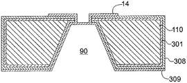
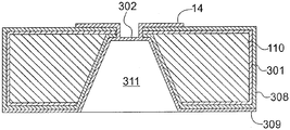
도 2a 및 도 2b는 본 발명의 바람직한 일 실시예에 따른 라인 2a 및 2b를 따라 절단된 도 1a 및 도 1c의 마이크로벤치들을 개략적으로 도시한 측단면도.
도 3a 및 도 3c는 본 발명의 바람직한 일 실시예에 따른 도 1a 내지 도 1c에 도시된 것보다 리세스된 영역들의 다른 배치를 가지는 마이크로벤치들의 부가적인 배열들을 도시한 측단면도.
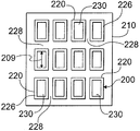
도 4a는 본 발명의 바람직한 일 실시예에 따른 복수의 광학 마이크로벤치들을 포함하는 베이스 웨이퍼를 개략적으로 도시한 평면도.
도 4b는 본 발명의 바람직한 일 실시예에 따른 복수의 리드들을 포함하는 웨이퍼를 개략적으로 도시한 평면도.
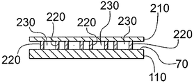
도 4c는 일련의 마이크로벤치들 중 하나를 따라 절단된 단면과 함께 도 4a의 베이스 웨이퍼 위로 밀봉된 도 4b의 리드 웨이퍼를 개략적으로 도시한 측단면도.
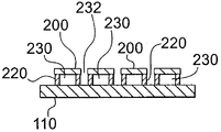
도 4d 내지 도 4f는 상기 리드들이 상기 리드 웨이퍼로부터 싱귤레이트된(singulated) 후 상기 조립된 리드 웨이퍼 및 도 4c의 베이스 웨이퍼를 각기 개략적으로 도시한 평면도 및 측단면도.
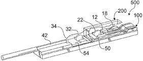
도 5b는 본 발명의 바람직한 일 실시예에 따른 도 5a에 도시된 구성 요소들로부터 조립된 마이크로 광학 장치 패키지를 개략적으로 도시한 사시도.
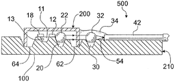
도 6a는 도 5a의 상기 마이크로 광학 장치 패키지의 광학축을 따라 절단된 측단면도를 개략적으로 도시한 도면.
도 6b는 도 6a에 도시된 것과 비슷한 마이크로 광학 장치 패키지의 광학축을 따라 절단된 측단면을 개략적으로 도시한 도면으로서, 레이저의 빛 발산 영역(light emitting region)을 섬유의 엔드페이스(endface) 위에 초점을 맞춘 싱글 렌즈들을 가지는 것을 도시함.
도 7a 내지 도 7c는 본 발명의 바람직한 일 실시예에 따른 다양한 냉각 구조들을 가지는 마이크로 광학 장치 패키지들을 개략적으로 도시한 측단면도.
도 8a 및 도 8b는 본 발명의 바람직한 일 실시예에 따른 마이크로 광학 장치 패키지들을 개략적으로 도시한 측단면도.
도 9a 및 도 9b는 본 발명의 바람직한 일 실시예에 따른 밀봉된 캐비티로부터 상기 패키지의 외부로 연장된 밀봉한 비아들(hermetic vias)을 가지는 마이크로 광학 장치 패키지들을 각기 개략적으로 도시한 측면도 및 평면도.
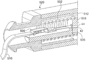
도 10a 및 도 10b는 본 발명의 바람직한 일 실시예에 따른 마이크로 광학 장치 패키지가 수용된(housed) 커넥터를 각기 개략적으로 도시한 측단면도 및 사시도
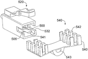
도 11a 내지 도 11c는 본 발명의 바람직한 일 실시예에 따른 마이크로 광학 장치 패키지를 냉각시키는 히트 싱크들(heat sinks)을 가지는 마이크로 광학 장치 패키지를 수용하는 커넥터들을 개략적으로 도시한 사시도.
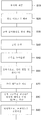
도 12a 및 도 12b는 본 발명의 바람직한 일 실시예에 따른 전도성 리드 라인들(conductive lead lines)을 가지는 광학 마이크로벤치를 제조하는 과정을 도시한 순서도.
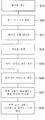
도 13a 내지 도 13c는 본 발명의 바람직한 일 실시예에 따른 도전성 밀봉 비아들(conductive hermetically sealed vias)을 가지는 광학 마이크로벤치를 제조하는 과정을 도시한 순서도.
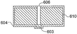
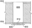
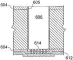
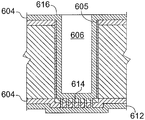
도 14a 내지 도 14g는 본 발명의 바람직한 일 실시예에 따른 도전성 밀봉 비아들을 제조하는 과정을 개략적으로 도시한 도면.
도 15a 내지 도 15i는 본 발명의 바람직한 일 실시예에 따른 도전성 밀봉 비아를 제조하는 다른 과정을 개략적으로 도시한 도면.
도 16a 내지 도 16d는 본 발명의 바람직한 일 실시예에 따른 리드 웨이퍼 위에 캐비테이트된 리드들(cavitated lids)을 제조하는 과정을 개략적으로 도시한 평면도.
도 17a 및 도 17b는 본 발명의 바람직한 다른 실시예에 따른 리드 웨이퍼 위에 캐비테이트된 리드들을 제조하는 다른 과정을 각기 개략적으로 도시한 평면도.
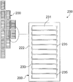
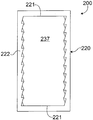
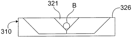
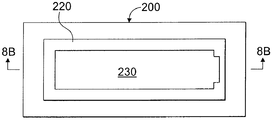
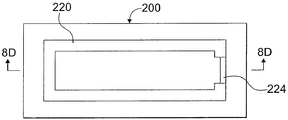
도 18a 내지 도 18d는 유리질의 측벽 부분을 가지는 리드를 개략적으로 도시한 도면.
12 광전자 장치
20, 30 피트
40 섬유 홈
50, 52, 54 리쎄스된 클리어런스 표면
60 리드 장착 영역
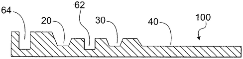
100 광학 마이크로벤치
110 베이스 웨이퍼
200 리드
220 측벽
300 리드
321 측벽
500 마이크로 광학 장치 패키지
Claims (7)
- 광전자 장치 장착 영역 및 리드 장착 영역을 각각 포함하는 다수의 베이스 다이를 포함하는 베이스 웨이퍼 또는 베이스 그리드;
각 광전자 장치 장착 영역 상에 장착된 광전자 장치; 및
베이스 웨이퍼 또는 베이스 그리드에 부착되며, 베이스 다이와 리드 다이 사이에 둘러싸여진 체적을 형성하기 위하여 각각의 리드 장착 영역 상에 각각 장착된 다수의 리드 다이를 포함하는 리드 웨이퍼 또는 리드 그리드를 포함하되,
각각의 광전자 장치는 둘러싸여진 체적 내에 있으며, 각 리드 다이는 광전자 장치로 또는 광전자 장치로부터 광학 경로를 따라 주어진 파장의 광을 전달하도록 구성된 광학적인 전달 영역을 갖는 웨이퍼 또는 그리드 레벨 광전자 장치 패키지. - 제 1 항에 있어서, 리드 웨이퍼 또는 리드 그리드는 실리콘 층들 사이에 배치된 글라스 층을 포함하는 실리콘-온-절연체 웨이퍼를 포함하며, 각 리드 다이는 실리콘 측벽 및 글라스를 포함하는 루프를 포함하는 웨이퍼 또는 그리드 레벨 광전자 장치 패키지.
- 다수의 다이를 포함하는 실리콘 웨이퍼 또는 그리드를 구비하며, 상기 다이의 각각은 다수의 측벽들 및 이 측벽들에 연결되어 캐비티를 형성하는 루프를 포함하여, 하나 또는 그 이상의 측벽은 측벽을 통하는 광학축을 따라 주어진 파장의 광을 전달하도록 구성된 광학적인 전달 영역을 포함하는 웨이퍼-또는 그리드-레벨 광전자 장치 패키지 리드.
- 제 3 항에 있어서, 광학적인 전달 영역 상의 비반사 코팅을 더 포함하는 웨이퍼-또는 그리드-레벨 광전자 장치 패키지 리드.
- 다수의 다이를 포함하는 실리콘 웨이퍼 또는 그리드를 제공하는 단계; 및
각 리드 구조체가 다수의 측벽들 및 이 측벽들에 연결되어 캐비티를 형성하는 루프를 포함하는 다수의 리드 구조체를 상기 웨이퍼 또는 그리드를 에칭하여 제조하는 단계를 구비하며,
각 리드 구조체의 하나 또는 그 이상의 측벽은 측벽을 통하는 광학축을 따라 주어진 파장의 광을 전달하도록 구성된 광학적인 전달 영역을 포함하는 웨이퍼 또는 그리드 레벨 상에 광전자 장치를 형성하는 방법. - 내부 캐비티와 광학 포트를 갖는 커넥터; 및
광학 포트와 광 연결 상태에서 캐비티 내에 배치된 광전자 장치 패키지를 포함하는 커넥터화된(connectorized) 광전자 장치. - 제6항에 있어서, 상기 광전자 장치 패키지는
광전자 장착 영역 및 리드 장착 영역을 포함하는 베이스 기판;
광전자 장착 영역 상에 장착된 광전자 장치; 및
베이스 기판과의 사이에 둘러싸여진 체적을 형성하기 위하여 리드 장착 영역 상에 장착된 리드를 포함하되,
상기 리드는 광전자 장치로 또는 광전자 장치로부터 광학 축을 따라 주어진 파장의 광을 전달하도록 구성된 광학적 전달 영역을 갖는 커넥터화된(connectorized) 광전자 장치.
Applications Claiming Priority (2)
| Application Number | Priority Date | Filing Date | Title |
|---|---|---|---|
| US50286803P | 2003-09-15 | 2003-09-15 | |
| US60/502,868 | 2003-09-15 |
Related Parent Applications (1)
| Application Number | Title | Priority Date | Filing Date |
|---|---|---|---|
| KR1020040073927A Division KR101146019B1 (ko) | 2003-09-15 | 2004-09-15 | 장치 패키지 및, 그 제조 방법 및 테스트 방법 |
Publications (2)
| Publication Number | Publication Date |
|---|---|
| KR20120042811A true KR20120042811A (ko) | 2012-05-03 |
| KR101264048B1 KR101264048B1 (ko) | 2013-05-21 |
Family
ID=34135393
Family Applications (4)
| Application Number | Title | Priority Date | Filing Date |
|---|---|---|---|
| KR1020040073927A Expired - Fee Related KR101146019B1 (ko) | 2003-09-15 | 2004-09-15 | 장치 패키지 및, 그 제조 방법 및 테스트 방법 |
| KR1020040073928A Expired - Fee Related KR101131654B1 (ko) | 2003-09-15 | 2004-09-15 | 장치 패키지 및, 그 제조 방법 및 테스트 방법 |
| KR1020110095176A Expired - Fee Related KR101194532B1 (ko) | 2003-09-15 | 2011-09-21 | 장치 패키지 및, 그 제조 방법 및 테스트 방법 |
| KR1020120030590A Expired - Fee Related KR101264048B1 (ko) | 2003-09-15 | 2012-03-26 | 장치 패키지, 그 제조 방법 및 테스트 방법 |
Family Applications Before (3)
| Application Number | Title | Priority Date | Filing Date |
|---|---|---|---|
| KR1020040073927A Expired - Fee Related KR101146019B1 (ko) | 2003-09-15 | 2004-09-15 | 장치 패키지 및, 그 제조 방법 및 테스트 방법 |
| KR1020040073928A Expired - Fee Related KR101131654B1 (ko) | 2003-09-15 | 2004-09-15 | 장치 패키지 및, 그 제조 방법 및 테스트 방법 |
| KR1020110095176A Expired - Fee Related KR101194532B1 (ko) | 2003-09-15 | 2011-09-21 | 장치 패키지 및, 그 제조 방법 및 테스트 방법 |
Country Status (7)
| Country | Link |
|---|---|
| US (11) | US7329056B2 (ko) |
| EP (3) | EP1515364B1 (ko) |
| JP (3) | JP4911885B2 (ko) |
| KR (4) | KR101146019B1 (ko) |
| CN (4) | CN100386867C (ko) |
| CA (5) | CA2843395C (ko) |
| TW (2) | TWI253761B (ko) |
Cited By (3)
| Publication number | Priority date | Publication date | Assignee | Title |
|---|---|---|---|---|
| KR20150136104A (ko) * | 2013-03-28 | 2015-12-04 | 오스람 옵토 세미컨덕터스 게엠베하 | 레이저 부품 및 그 제조 방법 |
| WO2017183851A1 (en) * | 2016-04-19 | 2017-10-26 | Opticis Co., Ltd. | Optical connector |
| WO2021003306A1 (en) * | 2019-07-02 | 2021-01-07 | Aayuna Inc. | Laser engine supporting multiple laser sources |
Families Citing this family (281)
| Publication number | Priority date | Publication date | Assignee | Title |
|---|---|---|---|---|
| US7233027B2 (en) * | 2001-04-30 | 2007-06-19 | Merge Optics Gmbh | Arrangement comprising at least two different electronic semiconductor circuits |
| US7073954B1 (en) * | 2001-09-17 | 2006-07-11 | Stratos International, Inc. | Transceiver assembly for use in fiber optics communications |
| AU2002360464A1 (en) | 2001-12-03 | 2003-06-17 | Memgen Corporation | Miniature rf and microwave components and methods for fabricating such components |
| US9614266B2 (en) | 2001-12-03 | 2017-04-04 | Microfabrica Inc. | Miniature RF and microwave components and methods for fabricating such components |
| US8971679B2 (en) * | 2002-08-28 | 2015-03-03 | Optonet Inc. | Apparatus and method for passive alignment of optical devices |
| ATE475999T1 (de) | 2003-03-04 | 2010-08-15 | Rohm & Haas Elect Mat | Koaxiale wellenleitermikrostrukturen und verfahern zu ihrer bildung |
| US10297421B1 (en) | 2003-05-07 | 2019-05-21 | Microfabrica Inc. | Plasma etching of dielectric sacrificial material from reentrant multi-layer metal structures |
| EP1515364B1 (en) | 2003-09-15 | 2016-04-13 | Nuvotronics, LLC | Device package and methods for the fabrication and testing thereof |
| US6985645B2 (en) * | 2003-09-24 | 2006-01-10 | International Business Machines Corporation | Apparatus and methods for integrally packaging optoelectronic devices, IC chips and optical transmission lines |
| US20050083982A1 (en) * | 2003-10-20 | 2005-04-21 | Binoptics Corporation | Surface emitting and receiving photonic device |
| US7333521B1 (en) * | 2003-12-04 | 2008-02-19 | National Semiconductor Corporation | Method of sensing VCSEL light output power by monitoring electrical characteristics of the VCSEL |
| US7616444B2 (en) | 2004-06-04 | 2009-11-10 | Cooligy Inc. | Gimballed attachment for multiple heat exchangers |
| US7045827B2 (en) * | 2004-06-24 | 2006-05-16 | Gallup Kendra J | Lids for wafer-scale optoelectronic packages |
| DE102004031878B3 (de) * | 2004-07-01 | 2005-10-06 | Epcos Ag | Elektrisches Mehrschichtbauelement mit zuverlässigem Lötkontakt |
| KR100594716B1 (ko) * | 2004-07-27 | 2006-06-30 | 삼성전자주식회사 | 공동부를 구비한 캡 웨이퍼, 이를 이용한 반도체 칩, 및그 제조방법 |
| US20060046501A1 (en) * | 2004-08-27 | 2006-03-02 | Texas Instruments Incorporated | Screening of electroless nickel/immersion gold-plated substrates with black pad defect |
| US7833834B2 (en) * | 2004-09-30 | 2010-11-16 | Sharp Kabushiki Kaisha | Method for producing nitride semiconductor laser light source and apparatus for producing nitride semiconductor laser light source |
| JP2006119024A (ja) * | 2004-10-22 | 2006-05-11 | Tokyo Electron Ltd | プローブおよびその製造方法 |
| JP4451371B2 (ja) * | 2004-12-20 | 2010-04-14 | シャープ株式会社 | 窒化物半導体レーザ素子 |
| US20060132544A1 (en) * | 2004-12-21 | 2006-06-22 | Corley Richard E Jr | Laser tacking and singulating method and system |
| US7630422B1 (en) | 2005-01-14 | 2009-12-08 | National Semiconductor Corporation | Driver for vertical-cavity surface-emitting laser and method |
| US8050526B2 (en) * | 2005-02-08 | 2011-11-01 | Samsung Electronics Co., Ltd. | Micro-optical device and method of making same |
| KR20060104531A (ko) * | 2005-03-30 | 2006-10-09 | 삼성에스디아이 주식회사 | 발광표시장치의 제조방법 |
| US7750356B2 (en) | 2005-05-04 | 2010-07-06 | Avago Technologies Fiber Ip (Singapore) Pte. Ltd. | Silicon optical package with 45 degree turning mirror |
| CA2548857C (en) * | 2005-06-01 | 2015-01-06 | Rohm And Haas Electronic Materials Llc | Optical assemblies |
| US7790484B2 (en) * | 2005-06-08 | 2010-09-07 | Sharp Kabushiki Kaisha | Method for manufacturing laser devices |
| US20070012661A1 (en) * | 2005-07-13 | 2007-01-18 | Vasilyeva Irina V | Silicon nitride passivation layers having oxidized interface |
| CA2556117A1 (en) * | 2005-08-15 | 2007-02-15 | Rohm And Haas Electronic Materials Llc | Bonding methods and optical assemblies |
| US7772116B2 (en) | 2005-09-01 | 2010-08-10 | Micron Technology, Inc. | Methods of forming blind wafer interconnects |
| US7572572B2 (en) * | 2005-09-01 | 2009-08-11 | Micron Technology, Inc. | Methods for forming arrays of small, closely spaced features |
| KR100713121B1 (ko) * | 2005-09-27 | 2007-05-02 | 한국전자통신연구원 | 칩과 이를 이용한 칩 스택 및 그 제조방법 |
| US7619312B2 (en) * | 2005-10-03 | 2009-11-17 | Sun Microsystems, Inc. | Method and apparatus for precisely aligning integrated circuit chips |
| TWI309313B (en) * | 2005-10-11 | 2009-05-01 | Rohm & Haas Elect Mat | Micro-optical device |
| US7913719B2 (en) * | 2006-01-30 | 2011-03-29 | Cooligy Inc. | Tape-wrapped multilayer tubing and methods for making the same |
| US7807547B2 (en) * | 2006-03-28 | 2010-10-05 | Innovative Micro Technology | Wafer bonding material with embedded rigid particles |
| JP2007294523A (ja) * | 2006-04-21 | 2007-11-08 | Oki Electric Ind Co Ltd | 表面実装型光結合器、その実装方法、及び、その製造方法 |
| US20070262051A1 (en) * | 2006-05-12 | 2007-11-15 | Advanced Chip Engineering Technology Inc. | Method of plasma etching with pattern mask |
| US20070279885A1 (en) * | 2006-05-31 | 2007-12-06 | Basavanhally Nagesh R | Backages with buried electrical feedthroughs |
| JP2008010659A (ja) * | 2006-06-29 | 2008-01-17 | Disco Abrasive Syst Ltd | ビアホールの加工方法 |
| EP2043204B1 (en) * | 2006-07-19 | 2016-05-04 | Nikon Corporation | Cassette for optical fiber amplifier, optical fiber amplifier and light source device |
| JP2008028143A (ja) * | 2006-07-21 | 2008-02-07 | Sumitomo Electric Ind Ltd | 光モジュール |
| US7531445B2 (en) * | 2006-09-26 | 2009-05-12 | Hymite A/S | Formation of through-wafer electrical interconnections and other structures using a thin dielectric membrane |
| US7589009B1 (en) * | 2006-10-02 | 2009-09-15 | Newport Fab, Llc | Method for fabricating a top conductive layer in a semiconductor die and related structure |
| US20080083611A1 (en) * | 2006-10-06 | 2008-04-10 | Tegal Corporation | High-adhesive backside metallization |
| US20080157353A1 (en) * | 2006-12-29 | 2008-07-03 | Texas Instruments Incorporated | Control of Standoff Height Between Packages with a Solder-Embedded Tape |
| JP2008188755A (ja) | 2006-12-30 | 2008-08-21 | Rohm & Haas Electronic Materials Llc | 三次元微細構造体およびその形成方法 |
| US20080181558A1 (en) * | 2007-01-31 | 2008-07-31 | Hartwell Peter G | Electronic and optical circuit integration through wafer bonding |
| JP4919984B2 (ja) * | 2007-02-25 | 2012-04-18 | サムスン エレクトロニクス カンパニー リミテッド | 電子デバイスパッケージとその形成方法 |
| JP5010948B2 (ja) * | 2007-03-06 | 2012-08-29 | オリンパス株式会社 | 半導体装置 |
| US7994594B2 (en) | 2007-03-15 | 2011-08-09 | Seiko Epson Corporation | Electronic device, resonator, oscillator and method for manufacturing electronic device |
| US7887243B2 (en) | 2007-03-16 | 2011-02-15 | Honeywell Federal Manufacturing & Technologies, Llc | Miniature mechanical transfer optical coupler |
| EP1973190A1 (en) | 2007-03-20 | 2008-09-24 | Rohm and Haas Electronic Materials LLC | Integrated electronic components and methods of formation thereof |
| EP1973189B1 (en) | 2007-03-20 | 2012-12-05 | Nuvotronics, LLC | Coaxial transmission line microstructures and methods of formation thereof |
| EP1986028A3 (en) * | 2007-03-27 | 2008-11-05 | Rohm and Haas Electronic Materials LLC | Optical assemblies and their methods of formation |
| US9018724B2 (en) * | 2007-03-28 | 2015-04-28 | Advancedmems Llp | Method of producing optical MEMS |
| SG148054A1 (en) * | 2007-05-17 | 2008-12-31 | Micron Technology Inc | Semiconductor packages and method for fabricating semiconductor packages with discrete components |
| US7923373B2 (en) | 2007-06-04 | 2011-04-12 | Micron Technology, Inc. | Pitch multiplication using self-assembling materials |
| US7919973B2 (en) * | 2007-06-22 | 2011-04-05 | Microchip Technology Incorporated | Method and apparatus for monitoring via's in a semiconductor fab |
| US20090026619A1 (en) * | 2007-07-24 | 2009-01-29 | Northrop Grumman Space & Mission Systems Corp. | Method for Backside Metallization for Semiconductor Substrate |
| USD597039S1 (en) * | 2007-11-09 | 2009-07-28 | Sanyo Electric Co., Ltd. | Light-emitting diode(LED) |
| USD597040S1 (en) * | 2007-11-09 | 2009-07-28 | Sanyo Electric Co., Ltd. | Light-emitting diode (LED) |
| US8217482B2 (en) * | 2007-12-21 | 2012-07-10 | Avago Technologies General Ip (Singapore) Pte. Ltd. | Infrared proximity sensor package with reduced crosstalk |
| JP2009259595A (ja) * | 2008-04-16 | 2009-11-05 | Hitachi Cable Ltd | 電気接点層付金属材およびその製造方法 |
| US20090279172A1 (en) * | 2008-05-12 | 2009-11-12 | Higashi Robert E | Microelectromechanical lamellar grating |
| US8490678B2 (en) * | 2008-06-02 | 2013-07-23 | Gerald Ho Kim | Silicon-based thermal energy transfer device and apparatus |
| JP2010010447A (ja) * | 2008-06-27 | 2010-01-14 | Disco Abrasive Syst Ltd | 半導体デバイスの電極形成方法 |
| WO2010009358A1 (en) * | 2008-07-17 | 2010-01-21 | Lawrence Pumps, Inc. | Apparatus for simultaneous support of pressurized and unpressurized mechanical shaft sealing barrier fluid systems |
| US8238401B2 (en) * | 2008-08-25 | 2012-08-07 | Gerald Ho Kim | Silicon-based lens support structure for diode laser |
| US7943411B2 (en) * | 2008-09-10 | 2011-05-17 | Analog Devices, Inc. | Apparatus and method of wafer bonding using compatible alloy |
| US8956904B2 (en) | 2008-09-10 | 2015-02-17 | Analog Devices, Inc. | Apparatus and method of wafer bonding using compatible alloy |
| DE102008058003B4 (de) * | 2008-11-19 | 2012-04-05 | Infineon Technologies Ag | Verfahren zur Herstellung eines Halbleitermoduls und Halbleitermodul |
| US20100127407A1 (en) * | 2008-11-25 | 2010-05-27 | Leblanc John | Two-sided substrateless multichip module and method of manufacturing same |
| JP5509216B2 (ja) * | 2008-12-12 | 2014-06-04 | フレゼニウス メディカル ケアー ドイチュラント ゲゼルシャフト ミット ベシュレンクテル ハフツング | 医療液体の処理装置及びその漏れ密封の試験方法 |
| JP5532611B2 (ja) * | 2009-01-23 | 2014-06-25 | 富士通セミコンダクター株式会社 | 半導体装置の製造方法及び設計支援装置 |
| JP5302020B2 (ja) * | 2009-01-26 | 2013-10-02 | 浜松ホトニクス株式会社 | 光モジュール |
| JP5389464B2 (ja) * | 2009-02-10 | 2014-01-15 | フリースケール セミコンダクター インコーポレイテッド | 半導体装置の製造方法 |
| US8659371B2 (en) * | 2009-03-03 | 2014-02-25 | Bae Systems Information And Electronic Systems Integration Inc. | Three-dimensional matrix structure for defining a coaxial transmission line channel |
| US8580596B2 (en) * | 2009-04-10 | 2013-11-12 | Nxp, B.V. | Front end micro cavity |
| US20100283138A1 (en) * | 2009-05-06 | 2010-11-11 | Analog Devices, Inc. | Nickel-Based Bonding of Semiconductor Wafers |
| US8420999B2 (en) * | 2009-05-08 | 2013-04-16 | Avago Technologies Ecbu Ip (Singapore) Pte. Ltd. | Metal shield and housing for optical proximity sensor with increased resistance to mechanical deformation |
| US8779361B2 (en) * | 2009-06-30 | 2014-07-15 | Avago Technologies General Ip (Singapore) Pte. Ltd. | Optical proximity sensor package with molded infrared light rejection barrier and infrared pass components |
| US8957380B2 (en) * | 2009-06-30 | 2015-02-17 | Avago Technologies General Ip (Singapore) Pte. Ltd. | Infrared attenuating or blocking layer in optical proximity sensor |
| US9525093B2 (en) | 2009-06-30 | 2016-12-20 | Avago Technologies General Ip (Singapore) Pte. Ltd. | Infrared attenuating or blocking layer in optical proximity sensor |
| US8143608B2 (en) * | 2009-09-10 | 2012-03-27 | Avago Technologies Ecbu Ip (Singapore) Pte. Ltd. | Package-on-package (POP) optical proximity sensor |
| US8350216B2 (en) * | 2009-09-10 | 2013-01-08 | Avago Technologies Ecbu Ip (Singapore) Pte. Ltd. | Miniaturized optical proximity sensor |
| US8716665B2 (en) * | 2009-09-10 | 2014-05-06 | Avago Technologies General Ip (Singapore) Pte. Ltd. | Compact optical proximity sensor with ball grid array and windowed substrate |
| US9733357B2 (en) * | 2009-11-23 | 2017-08-15 | Avago Technologies General Ip (Singapore) Pte. Ltd. | Infrared proximity sensor package with improved crosstalk isolation |
| US20110123783A1 (en) * | 2009-11-23 | 2011-05-26 | David Sherrer | Multilayer build processses and devices thereof |
| US8917150B2 (en) * | 2010-01-22 | 2014-12-23 | Nuvotronics, Llc | Waveguide balun having waveguide structures disposed over a ground plane and having probes located in channels |
| KR101917052B1 (ko) * | 2010-01-22 | 2019-01-30 | 누보트로닉스, 인크. | 열관리 |
| US8669569B2 (en) * | 2010-02-04 | 2014-03-11 | Yu-Nung Shen | Light emitting diode package and method for fabricating the same |
| CN102148202B (zh) * | 2010-02-09 | 2016-06-08 | 精材科技股份有限公司 | 晶片封装体及其形成方法 |
| JP2013519917A (ja) * | 2010-02-12 | 2013-05-30 | エーゲンライト・コーポレーション | 一列に並んだ光ファイバーデバイス用のリード線付き貫通接続部を有する気密性パッケージおよび作製方法 |
| TWI419383B (zh) * | 2010-03-08 | 2013-12-11 | Harvatek Corp | 具有高效率散熱效果之發光二極體結構及其製作方法 |
| KR101637581B1 (ko) * | 2010-03-09 | 2016-07-07 | 엘지이노텍 주식회사 | 발광 소자 패키지 및 그 제조방법 |
| CN102237632A (zh) * | 2010-04-26 | 2011-11-09 | 无锡亮源激光技术有限公司 | 户外用半导体激光模块 |
| US20110285840A1 (en) * | 2010-05-20 | 2011-11-24 | Applied Materials, Inc. | Solder bonding and inspection method and apparatus |
| DE102010029760B4 (de) * | 2010-06-07 | 2019-02-21 | Robert Bosch Gmbh | Bauelement mit einer Durchkontaktierung und Verfahren zu seiner Herstellung |
| US9341792B2 (en) | 2010-06-29 | 2016-05-17 | Cisco Technology, Inc. | Vent structures for encapsulated components on an SOI-based photonics platform |
| WO2012020380A1 (en) | 2010-08-11 | 2012-02-16 | Primesense Ltd. | Scanning projectors and image capture modules for 3d mapping |
| US10739460B2 (en) | 2010-08-11 | 2020-08-11 | Apple Inc. | Time-of-flight detector with single-axis scan |
| US8528397B2 (en) * | 2010-08-18 | 2013-09-10 | International Business Machines Corporation | Hermeticity sensor and related method |
| CN101997269B (zh) * | 2010-09-15 | 2012-02-08 | 山东华光光电子有限公司 | 一种半导体激光器巴条制作方法 |
| GB2484486A (en) * | 2010-10-12 | 2012-04-18 | Oclaro Technology Ltd | Component Temperature Control |
| KR101430634B1 (ko) | 2010-11-19 | 2014-08-18 | 한국전자통신연구원 | 광 모듈 |
| CN102055132A (zh) * | 2010-11-26 | 2011-05-11 | 中国科学院物理研究所 | 可深度冷却的半导体激光器装置及其密封装置 |
| JP2012137597A (ja) * | 2010-12-27 | 2012-07-19 | Fujitsu Ltd | 光デバイス、光送受信ユニットおよび光通信システム |
| US8841597B2 (en) | 2010-12-27 | 2014-09-23 | Avago Technologies Ip (Singapore) Pte. Ltd. | Housing for optical proximity sensor |
| US8582618B2 (en) | 2011-01-18 | 2013-11-12 | Avago Technologies General Ip (Singapore) Pte. Ltd. | Surface-emitting semiconductor laser device in which an edge-emitting laser is integrated with a diffractive or refractive lens on the semiconductor laser device |
| JP5964813B2 (ja) | 2011-03-24 | 2016-08-03 | シスメックス株式会社 | 検体分析装置、検体情報処理装置および検体分析方法 |
| US8315287B1 (en) | 2011-05-03 | 2012-11-20 | Avago Technologies Fiber Ip (Singapore) Pte. Ltd | Surface-emitting semiconductor laser device in which an edge-emitting laser is integrated with a diffractive lens, and a method for making the device |
| JP5583632B2 (ja) * | 2011-05-13 | 2014-09-03 | Nttエレクトロニクス株式会社 | 光モジュール |
| US8866300B1 (en) | 2011-06-05 | 2014-10-21 | Nuvotronics, Llc | Devices and methods for solder flow control in three-dimensional microstructures |
| US8814601B1 (en) | 2011-06-06 | 2014-08-26 | Nuvotronics, Llc | Batch fabricated microconnectors |
| US20120319710A1 (en) * | 2011-06-15 | 2012-12-20 | Probelogic, Inc. | Method and apparatus for implementing probes for electronic circuit testing |
| JP6335782B2 (ja) | 2011-07-13 | 2018-05-30 | ヌボトロニクス、インク. | 電子的および機械的な構造を製作する方法 |
| GB2494640A (en) * | 2011-09-13 | 2013-03-20 | Zinir Ltd | Optical substrate with recesses for passive alignment of optical components |
| US9052445B2 (en) | 2011-10-19 | 2015-06-09 | Cisco Technology, Inc. | Molded glass lid for wafer level packaging of opto-electronic assemblies |
| JP6040253B2 (ja) * | 2011-10-20 | 2016-12-07 | シーウェア システムズSi−Ware Systems | 3d湾曲光素子を含む集積化されたモノリシック光ベンチ、及びその作製方法 |
| US8426227B1 (en) | 2011-11-18 | 2013-04-23 | LuxVue Technology Corporation | Method of forming a micro light emitting diode array |
| US8349116B1 (en) | 2011-11-18 | 2013-01-08 | LuxVue Technology Corporation | Micro device transfer head heater assembly and method of transferring a micro device |
| CN103163361B (zh) * | 2011-12-13 | 2015-10-21 | 英业达股份有限公司 | 电子元件与检测系统的组合与电子元件的检测方法 |
| US9773750B2 (en) * | 2012-02-09 | 2017-09-26 | Apple Inc. | Method of transferring and bonding an array of micro devices |
| US9651417B2 (en) * | 2012-02-15 | 2017-05-16 | Apple Inc. | Scanning depth engine |
| US9981844B2 (en) * | 2012-03-08 | 2018-05-29 | Infineon Technologies Ag | Method of manufacturing semiconductor device with glass pieces |
| CN104205366B (zh) * | 2012-03-30 | 2018-08-31 | 亮锐控股有限公司 | 密封的半导体发光器件 |
| CN107565374B (zh) | 2012-05-08 | 2020-08-07 | 镁可微波技术有限公司 | 具有光束形状修改的激光器 |
| US9500808B2 (en) | 2012-05-09 | 2016-11-22 | The Boeing Company | Ruggedized photonic crystal sensor packaging |
| WO2013183272A1 (ja) * | 2012-06-05 | 2013-12-12 | 株式会社エンプラス | 光レセプタクルおよびこれを備えた光モジュール |
| US9165723B2 (en) | 2012-08-23 | 2015-10-20 | Harris Corporation | Switches for use in microelectromechanical and other systems, and processes for making same |
| US9053873B2 (en) | 2012-09-20 | 2015-06-09 | Harris Corporation | Switches for use in microelectromechanical and other systems, and processes for making same |
| US9053874B2 (en) | 2012-09-20 | 2015-06-09 | Harris Corporation | MEMS switches and other miniaturized devices having encapsulating enclosures, and processes for fabricating same |
| US20140082935A1 (en) * | 2012-09-27 | 2014-03-27 | Volex Plc | Method for passive alignment of optical components to a substrate |
| KR102094995B1 (ko) * | 2012-10-08 | 2020-03-31 | 삼성전자주식회사 | 열전모듈, 이를 구비한 열전장치, 및 열전모듈의 제조방법 |
| JP6247495B2 (ja) * | 2012-11-26 | 2017-12-13 | キヤノン株式会社 | 半導体装置、及びその製造方法 |
| US9325044B2 (en) | 2013-01-26 | 2016-04-26 | Nuvotronics, Inc. | Multi-layer digital elliptic filter and method |
| TW201430430A (zh) * | 2013-01-31 | 2014-08-01 | Hon Hai Prec Ind Co Ltd | 光通訊模組 |
| US9306254B1 (en) | 2013-03-15 | 2016-04-05 | Nuvotronics, Inc. | Substrate-free mechanical interconnection of electronic sub-systems using a spring configuration |
| EP2972081B1 (en) | 2013-03-15 | 2020-04-22 | Apple Inc. | Depth scanning with multiple emitters |
| US9306255B1 (en) | 2013-03-15 | 2016-04-05 | Nuvotronics, Inc. | Microstructure including microstructural waveguide elements and/or IC chips that are mechanically interconnected to each other |
| US9090461B2 (en) | 2013-04-30 | 2015-07-28 | Hewlett-Packard Development Company, L.P. | Temporary optical wave diffusion-promoting film adhered to lidded MEMS wafer for testing using interferometer |
| US9040386B2 (en) * | 2013-07-23 | 2015-05-26 | Maxim Integrated Products, Inc. | Method for varied topographic MEMS cap process |
| US9246592B2 (en) * | 2013-08-19 | 2016-01-26 | International Business Machines Corporation | Structured substrate for optical fiber alignment |
| CN103454052B (zh) * | 2013-08-29 | 2017-03-01 | 上海华虹宏力半导体制造有限公司 | Mems器件及晶圆级密封性的测量方法 |
| US9810641B2 (en) * | 2013-09-03 | 2017-11-07 | Kulicke & Soffa Industries, Inc. | Systems and methods for measuring physical characteristics of semiconductor device elements using structured light |
| CN103647004B (zh) * | 2013-11-28 | 2016-05-11 | 苏州百奥丽光电科技有限公司 | Led灯管的烘烤装置 |
| US10056294B2 (en) * | 2013-12-02 | 2018-08-21 | Maxim Integrated Products, Inc. | Techniques for adhesive control between a substrate and a die |
| WO2015104715A1 (en) * | 2014-01-13 | 2015-07-16 | Corning Optical Communications Wireless Ltd. | Dissipating heat from electronic devices |
| US9308596B2 (en) * | 2014-01-17 | 2016-04-12 | Alcatel Lucent | Method and assembly including a connection between metal layers and a fusible material |
| WO2015109208A2 (en) | 2014-01-17 | 2015-07-23 | Nuvotronics, Llc | Wafer scale test interface unit: low loss and high isolation devices and methods for high speed and high density mixed signal interconnects and contactors |
| US9389378B2 (en) * | 2014-02-03 | 2016-07-12 | Luxtera, Inc. | Method and system for optical power monitoring of a light source assembly coupled to a silicon photonically-enabled integrated circuit |
| US9563021B2 (en) | 2014-03-17 | 2017-02-07 | Lumentum Operations Llc | Optical switching device |
| US9930793B2 (en) | 2014-03-27 | 2018-03-27 | Intel Corporation | Electric circuit on flexible substrate |
| CN104948476B (zh) * | 2014-03-31 | 2020-06-02 | 台达电子工业股份有限公司 | 薄型风扇、电子系统及薄型风扇的制造方法 |
| US8999816B1 (en) * | 2014-04-18 | 2015-04-07 | Applied Materials, Inc. | Pre-patterned dry laminate mask for wafer dicing processes |
| US10847469B2 (en) | 2016-04-26 | 2020-11-24 | Cubic Corporation | CTE compensation for wafer-level and chip-scale packages and assemblies |
| US10511073B2 (en) | 2014-12-03 | 2019-12-17 | Cubic Corporation | Systems and methods for manufacturing stacked circuits and transmission lines |
| US20160302335A1 (en) * | 2015-04-10 | 2016-10-13 | Mettler-Toledo Autochem, Inc. | Precision mounting systems and methods |
| US9525863B2 (en) | 2015-04-29 | 2016-12-20 | Apple Inc. | Time-of-flight depth mapping with flexible scan pattern |
| US9478494B1 (en) | 2015-05-12 | 2016-10-25 | Harris Corporation | Digital data device interconnects |
| US9551831B1 (en) * | 2015-05-18 | 2017-01-24 | Alliance Fiber Optic Products, Inc. | Pluggable LC adaptor having optical passive element |
| US9437911B1 (en) | 2015-05-21 | 2016-09-06 | Harris Corporation | Compliant high speed interconnects |
| JP6661901B2 (ja) * | 2015-06-22 | 2020-03-11 | 住友電気工業株式会社 | 光モジュール、光モジュールを作製する方法 |
| US10315915B2 (en) * | 2015-07-02 | 2019-06-11 | Kionix, Inc. | Electronic systems with through-substrate interconnects and MEMS device |
| JP6551008B2 (ja) * | 2015-07-27 | 2019-07-31 | 住友電気工業株式会社 | 光モジュール、光学装置 |
| JP6354704B2 (ja) * | 2015-08-25 | 2018-07-11 | 日亜化学工業株式会社 | 光学部材の製造方法、半導体レーザ装置の製造方法及び半導体レーザ装置 |
| DE102015114292A1 (de) | 2015-08-27 | 2017-03-02 | Osram Opto Semiconductors Gmbh | Laserbauelement und Verfahren zu seiner Herstellung |
| US10508345B2 (en) * | 2015-10-08 | 2019-12-17 | Taiwan Semiconductor Manufacturing Company Ltd. | Sensor in an internet-of-things and manufacturing method of the same |
| JP6854242B2 (ja) * | 2015-10-20 | 2021-04-07 | ヌヴォトンテクノロジージャパン株式会社 | 光源装置及び投光装置 |
| CN105304586A (zh) * | 2015-11-20 | 2016-02-03 | 江阴长电先进封装有限公司 | 一种带有加强结构的芯片嵌入式封装结构及其封装方法 |
| JP6489001B2 (ja) * | 2015-12-09 | 2019-03-27 | 住友電気工業株式会社 | 光モジュール、光モジュールを作製する方法、及び光学装置 |
| US10120133B2 (en) * | 2015-12-18 | 2018-11-06 | Mellanox Technologies Silicon Photonics Inc. | Edge construction on optical devices |
| US10324171B2 (en) | 2015-12-20 | 2019-06-18 | Apple Inc. | Light detection and ranging sensor |
| US9773764B2 (en) * | 2015-12-22 | 2017-09-26 | Intel Corporation | Solid state device miniaturization |
| US9638859B1 (en) | 2016-01-12 | 2017-05-02 | Elenion Technologies, Llc | Optical fiber alignment device |
| US10234626B2 (en) * | 2016-02-08 | 2019-03-19 | Skorpios Technologies, Inc. | Stepped optical bridge for connecting semiconductor waveguides |
| FR3047842B1 (fr) * | 2016-02-12 | 2018-05-18 | Commissariat A L'energie Atomique Et Aux Energies Alternatives | Composant electronique a resistance metallique suspendue dans une cavite fermee |
| US10453760B2 (en) * | 2016-04-08 | 2019-10-22 | Advanced Semiconductor Engineering, Inc. | Lid array panel, package with lid and method of making the same |
| JP6636377B2 (ja) * | 2016-04-08 | 2020-01-29 | 株式会社ディスコ | パッケージウェーハの製造方法及びデバイスチップの製造方法 |
| CN109075526B (zh) * | 2016-04-18 | 2022-05-31 | 京瓷株式会社 | 发光元件收纳用构件及发光装置 |
| US9684141B1 (en) * | 2016-04-25 | 2017-06-20 | Applied Optoelectronics, Inc. | Techniques for reducing ingress of foreign matter into an optical subassembly |
| WO2017203785A1 (ja) * | 2016-05-23 | 2017-11-30 | オリンパス株式会社 | 光信号送信モジュール |
| WO2017203786A1 (ja) * | 2016-05-23 | 2017-11-30 | オリンパス株式会社 | 光信号送信モジュール |
| US10082271B2 (en) | 2016-06-29 | 2018-09-25 | Nichia Corporation | Laser light optical module utilizing reflective films for improved efficiency |
| US10168555B1 (en) | 2016-06-30 | 2019-01-01 | Google Llc | Wiring in a head-mountable device |
| US10298913B2 (en) | 2016-08-18 | 2019-05-21 | Apple Inc. | Standalone depth camera |
| US10539815B2 (en) | 2016-09-22 | 2020-01-21 | Mellanox Technologies Silicon Photonics Inc. | Edge construction on optical devices |
| US9835801B1 (en) | 2016-09-22 | 2017-12-05 | Mellanox Technologies Silicon Photonics Inc. | Edge construction on optical devices |
| KR101929465B1 (ko) * | 2016-10-18 | 2019-03-14 | 주식회사 옵텔라 | 광학모듈 |
| EP4166060A3 (en) * | 2016-12-22 | 2023-07-26 | Magic Leap, Inc. | Methods and systems for fabrication of shaped fiber elements for scanning fiber displays |
| US10782315B2 (en) | 2017-04-17 | 2020-09-22 | Rosemount Aerospace Inc. | Apparatus and method for packaging, handling or testing of sensors |
| US10193302B2 (en) * | 2017-05-10 | 2019-01-29 | Applied Optoelectronics, Inc. | Light engine with integrated turning mirror for direct coupling to photonically-enabled complementary metal-oxide semiconductor (CMOS) die |
| US10209477B1 (en) * | 2017-05-25 | 2019-02-19 | Lockheed Martin Coherent Technologies, Inc. | Systems and methods for reconfigurable micro-optic assemblies |
| EP3662311A1 (en) * | 2017-08-01 | 2020-06-10 | Rockley Photonics Limited | Module with transmit optical subassembly and receive optical subassembly |
| JP6958098B2 (ja) * | 2017-08-10 | 2021-11-02 | 住友電気工業株式会社 | 光モジュール |
| CN107422433A (zh) * | 2017-09-08 | 2017-12-01 | 中航海信光电技术有限公司 | 一种集成多光口的psm光电收发器件 |
| RU181835U1 (ru) * | 2017-09-14 | 2018-07-26 | Российская Федерация, от имени которой выступает ФОНД ПЕРСПЕКТИВНЫХ ИССЛЕДОВАНИЙ | Защитные покрытия различного назначения места установки датчиков на поверхности конструкции |
| US10634717B2 (en) * | 2017-09-29 | 2020-04-28 | Taiwan Semiconductor Manufacturing Co., Ltd. | Testing apparatus and testing method |
| US10514511B2 (en) * | 2017-11-02 | 2019-12-24 | Panduit Corp. | Optical fiber termination using a reference source |
| US10319654B1 (en) | 2017-12-01 | 2019-06-11 | Cubic Corporation | Integrated chip scale packages |
| CN108323151B (zh) * | 2018-01-29 | 2023-12-19 | 广东利元亨智能装备有限公司 | 一种烟雾报警器自动组装生产线 |
| US10921447B2 (en) | 2018-01-29 | 2021-02-16 | Rohm Co., Ltd. | Control circuit of light emitting and receiving device |
| US20190278036A1 (en) * | 2018-03-07 | 2019-09-12 | Lightwave Logic Inc. | Embedded hermetic capsule and method |
| US11427731B2 (en) | 2018-03-23 | 2022-08-30 | Teledyne Micralyne, Inc. | Adhesive silicon oxynitride film |
| US11373849B2 (en) | 2018-05-31 | 2022-06-28 | Micromass Uk Limited | Mass spectrometer having fragmentation region |
| WO2019229469A1 (en) | 2018-05-31 | 2019-12-05 | Micromass Uk Limited | Mass spectrometer |
| GB201808936D0 (en) | 2018-05-31 | 2018-07-18 | Micromass Ltd | Bench-top time of flight mass spectrometer |
| GB201808912D0 (en) | 2018-05-31 | 2018-07-18 | Micromass Ltd | Bench-top time of flight mass spectrometer |
| GB201808894D0 (en) | 2018-05-31 | 2018-07-18 | Micromass Ltd | Mass spectrometer |
| GB201808949D0 (en) | 2018-05-31 | 2018-07-18 | Micromass Ltd | Bench-top time of flight mass spectrometer |
| GB201808932D0 (en) | 2018-05-31 | 2018-07-18 | Micromass Ltd | Bench-top time of flight mass spectrometer |
| GB201808892D0 (en) | 2018-05-31 | 2018-07-18 | Micromass Ltd | Mass spectrometer |
| GB201808890D0 (en) | 2018-05-31 | 2018-07-18 | Micromass Ltd | Bench-top time of flight mass spectrometer |
| GB201808893D0 (en) | 2018-05-31 | 2018-07-18 | Micromass Ltd | Bench-top time of flight mass spectrometer |
| US11953728B2 (en) | 2018-08-06 | 2024-04-09 | Rockley Photonics Limited | Method for III-v/silicon hybrid integration |
| US11036005B2 (en) * | 2018-08-06 | 2021-06-15 | Rockley Photonics Limited | Method for III-V/silicon hybrid integration |
| US11378762B2 (en) | 2018-08-06 | 2022-07-05 | Rockley Photonics Limited | Method for III-V/silicon hybrid integration |
| US11398406B2 (en) * | 2018-09-28 | 2022-07-26 | Taiwan Semiconductor Manufacturing Company, Ltd. | Selective deposition of metal barrier in damascene processes |
| US12009633B2 (en) * | 2018-10-17 | 2024-06-11 | Osram Opto Semiconductors Gmbh | Laser device and method for manufacturing a laser device |
| US10712500B2 (en) * | 2018-10-17 | 2020-07-14 | Taiwan Semiconductor Manufacturing Company Ltd. | Semiconductor device and manufacturing method of the same |
| CN108957649B (zh) * | 2018-10-17 | 2023-08-22 | 四川光恒通信技术有限公司 | 一种平行光结构双收双发盒型密封封装光器件 |
| US11075173B2 (en) * | 2018-10-31 | 2021-07-27 | Taiwan Semiconductor Manufacturing Company, Ltd. | Semiconductor device and method of forming same |
| RU2698561C1 (ru) * | 2018-12-03 | 2019-08-28 | Федеральное государственное бюджетное образовательное учреждение высшего образования "Саратовский национальный исследовательский государственный университет имени Н.Г. Чернышевского" | СВЧ фотонный кристалл |
| KR102052737B1 (ko) * | 2018-12-15 | 2020-01-08 | 김현철 | 번인 공정용 포켓캐리어 플레이트 제조방법 및 이를 이용한 포켓캐리어 플레이트와 지그 조립체 |
| RU187926U1 (ru) * | 2019-01-10 | 2019-03-25 | Закрытое акционерное общество "ГРУППА КРЕМНИЙ ЭЛ" | Выводная рамка полупроводникового прибора |
| US11342256B2 (en) | 2019-01-24 | 2022-05-24 | Applied Materials, Inc. | Method of fine redistribution interconnect formation for advanced packaging applications |
| IT201900006736A1 (it) | 2019-05-10 | 2020-11-10 | Applied Materials Inc | Procedimenti di fabbricazione di package |
| IT201900006740A1 (it) | 2019-05-10 | 2020-11-10 | Applied Materials Inc | Procedimenti di strutturazione di substrati |
| EP3971623A4 (en) * | 2019-05-13 | 2023-09-06 | Lipac Co., Ltd. | CONNECTOR PLUG AND ACTIVE OPTICAL CABLE ASSEMBLY USING THE SAME |
| CN110296648B (zh) * | 2019-06-12 | 2024-07-09 | 浙江万向精工有限公司 | 轮毂轴承单元密封圈接触状态观测装置与方法 |
| US11931855B2 (en) | 2019-06-17 | 2024-03-19 | Applied Materials, Inc. | Planarization methods for packaging substrates |
| CN112114207B (zh) * | 2019-06-19 | 2024-05-10 | 泰克元有限公司 | 测试板及测试腔室 |
| JP7339062B2 (ja) * | 2019-08-09 | 2023-09-05 | 東京エレクトロン株式会社 | 載置台及び基板処理装置 |
| US11258229B2 (en) * | 2019-08-16 | 2022-02-22 | Cisco Technology, Inc. | Thermal gel application on electronic and optical components |
| US11862546B2 (en) | 2019-11-27 | 2024-01-02 | Applied Materials, Inc. | Package core assembly and fabrication methods |
| US11367664B2 (en) * | 2019-12-19 | 2022-06-21 | Amkor Technology Japan, Inc. | Semiconductor devices and methods of manufacturing semiconductor devices |
| KR102732446B1 (ko) * | 2020-01-17 | 2024-11-21 | 삼성전자주식회사 | 배선 구조물 및 이를 포함하는 수직형 메모리 장치 |
| JP7470517B2 (ja) * | 2020-02-05 | 2024-04-18 | 古河電気工業株式会社 | 光学装置 |
| US11257790B2 (en) | 2020-03-10 | 2022-02-22 | Applied Materials, Inc. | High connectivity device stacking |
| CN113410747B (zh) * | 2020-03-17 | 2022-07-12 | 潍坊华光光电子有限公司 | 一种半导体激光器管脚快速修复装置及修复方法 |
| US11454884B2 (en) | 2020-04-15 | 2022-09-27 | Applied Materials, Inc. | Fluoropolymer stamp fabrication method |
| EP4136719A1 (en) * | 2020-04-15 | 2023-02-22 | Excelitas Canada, Inc. | Hermetic surface mount package for semiconductor side emitting laser and method forming same |
| US11400545B2 (en) | 2020-05-11 | 2022-08-02 | Applied Materials, Inc. | Laser ablation for package fabrication |
| US11994718B2 (en) * | 2020-05-20 | 2024-05-28 | Lumentum Operations Llc | Mach-Zehnder interferometer with mirrored facet |
| US11676955B2 (en) | 2020-06-10 | 2023-06-13 | Micron Technology, Inc. | Separation method and assembly for chip-on-wafer processing |
| US11232951B1 (en) | 2020-07-14 | 2022-01-25 | Applied Materials, Inc. | Method and apparatus for laser drilling blind vias |
| US11676832B2 (en) | 2020-07-24 | 2023-06-13 | Applied Materials, Inc. | Laser ablation system for package fabrication |
| US11747396B2 (en) * | 2020-07-30 | 2023-09-05 | Openlight Photonics, Inc. | Optical interconnections for hybrid testing using automated testing equipment |
| US12206032B2 (en) | 2020-07-31 | 2025-01-21 | Apple Inc. | Wideband back-illuminated electromagnetic radiation detectors |
| CN114077016B (zh) | 2020-08-11 | 2023-09-01 | 美国莫列斯有限公司 | 具有光子集成电路的封装结构 |
| TWI725908B (zh) | 2020-08-18 | 2021-04-21 | 合晶科技股份有限公司 | 半極性氮化鎵的製作方法 |
| US12298573B1 (en) * | 2020-10-12 | 2025-05-13 | Poet Technologies, Inc. | Self-aligned structure and method on interposer-based PIC |
| CN112504574A (zh) * | 2020-10-28 | 2021-03-16 | 北京中科科仪股份有限公司 | 一种光阑调节装置的检测工装及检测系统 |
| US11521937B2 (en) | 2020-11-16 | 2022-12-06 | Applied Materials, Inc. | Package structures with built-in EMI shielding |
| US11404318B2 (en) | 2020-11-20 | 2022-08-02 | Applied Materials, Inc. | Methods of forming through-silicon vias in substrates for advanced packaging |
| DE102020215033A1 (de) * | 2020-11-30 | 2022-06-02 | Robert Bosch Gesellschaft mit beschränkter Haftung | Laserdiodenvorrichtung |
| JP2022094172A (ja) * | 2020-12-14 | 2022-06-24 | パナソニックIpマネジメント株式会社 | 発光装置、製造方法、及び導波構造体 |
| US11474301B2 (en) * | 2021-01-07 | 2022-10-18 | Advanced Semiconductor Engineering, Inc. | Device for communication |
| US12125865B2 (en) | 2021-03-31 | 2024-10-22 | Apple Inc. | Electromagnetic radiation detectors integrated with immersion lenses |
| CN113295382B (zh) * | 2021-04-29 | 2022-06-10 | 成都新锐鑫光通信技术有限公司 | 一种能够进行自适应检测的光纤连接器 |
| CN115342842A (zh) * | 2021-05-14 | 2022-11-15 | 中国海洋大学 | 一种微光纤同轴马赫泽德干涉仪传感器的封装方法 |
| US11705365B2 (en) | 2021-05-18 | 2023-07-18 | Applied Materials, Inc. | Methods of micro-via formation for advanced packaging |
| US11502757B1 (en) * | 2021-07-28 | 2022-11-15 | QuantumZ Inc. | Method of manufacturing device with optical component disposed thereon and transmission device manufactured by the same |
| US12094986B1 (en) | 2021-08-25 | 2024-09-17 | Apple Inc. | Quantum-efficiency enhanced optical detector pixel having one or more optical scattering structures |
| CN113834527B (zh) * | 2021-09-18 | 2024-09-27 | 重庆大学 | 一种压接型功率半导体结构及其内部压力在线测量方法 |
| US12399334B2 (en) | 2021-09-22 | 2025-08-26 | Intel Corporation | Photonic integrated circuit packaging architectures |
| US20230089877A1 (en) * | 2021-09-22 | 2023-03-23 | Intel Corporation | Photonic integrated circuit packaging architectures |
| US12392970B2 (en) | 2021-09-22 | 2025-08-19 | Intel Corporation | Photonic integrated circuit packaging architectures |
| US20250226637A1 (en) * | 2021-10-15 | 2025-07-10 | Ams-Osram International Gmbh | Optoelectronic device |
| US12183684B2 (en) | 2021-10-26 | 2024-12-31 | Applied Materials, Inc. | Semiconductor device packaging methods |
| US20230238770A1 (en) * | 2022-01-24 | 2023-07-27 | Materion Corporation | Semiconductor package for an edge emitting laser diode |
| CN114705229A (zh) * | 2022-03-29 | 2022-07-05 | 深圳市联创杰科技有限公司 | 一种基于敏感材料的基底可调光纤fp复合温湿度传感器芯片 |
| CN115032741A (zh) * | 2022-05-22 | 2022-09-09 | 上海图灵智算量子科技有限公司 | 波导及包含其的光芯片 |
| CN115767948B (zh) * | 2022-11-14 | 2024-04-02 | 北京自动化控制设备研究所 | Mems惯性系统高密度低应力集成方法 |
| WO2025026974A1 (en) * | 2023-08-01 | 2025-02-06 | Ams-Osram International Gmbh | Method for producing an electronic device and electronic device |
| TWI853720B (zh) * | 2023-09-26 | 2024-08-21 | 前鼎光電股份有限公司 | 電子裝置 |
| CN117103697A (zh) * | 2023-10-20 | 2023-11-24 | 成都光创联科技有限公司 | 一种气密光器件的生产方法 |
| WO2025155980A1 (en) * | 2024-01-19 | 2025-07-24 | The Johns Hopkins University | System and method for ultrahigh temperature testing of a physical property of a sample |
| CN118096767B (zh) * | 2024-04-28 | 2024-07-23 | 成都数之联科技股份有限公司 | 一种晶圆切割不良缺陷检测方法、系统、设备及存储介质 |
| CN119310684A (zh) * | 2024-12-19 | 2025-01-14 | 中国科学院长春光学精密机械与物理研究所 | 全玻璃单模保偏光纤准直器及其制备方法 |
| CN119456460B (zh) * | 2025-01-10 | 2025-05-09 | 珠海市申科谱工业科技有限公司 | 光波导片检测分选设备 |
Family Cites Families (172)
| Publication number | Priority date | Publication date | Assignee | Title |
|---|---|---|---|---|
| US73145A (en) | 1868-01-07 | wellman | ||
| US731445A (en) * | 1902-09-16 | 1903-06-23 | Willis M Esterly | Laundry clothes-drier. |
| GB2136203B (en) | 1983-03-02 | 1986-10-15 | Standard Telephones Cables Ltd | Through-wafer integrated circuit connections |
| US4771630A (en) | 1985-12-20 | 1988-09-20 | Warner-Lambert Company | Method and apparatus for testing hermetic seal integrity of sealed packages and containers |
| JPH0620705Y2 (ja) | 1987-09-29 | 1994-06-01 | 油谷重工株式会社 | 内装材の取付構造 |
| US4897711A (en) * | 1988-03-03 | 1990-01-30 | American Telephone And Telegraph Company | Subassembly for optoelectronic devices |
| US5082339A (en) * | 1988-07-11 | 1992-01-21 | Telefunken Electronic Gmbh | Optical read-write head with diffraction grating structure |
| EP0448713B1 (en) | 1988-07-22 | 1993-10-27 | Nippondenso Co., Ltd. | Semiconductor device |
| JPH0253007A (ja) * | 1988-08-18 | 1990-02-22 | Matsushita Electric Ind Co Ltd | 半導体レーザと光ファイバとの結合方法 |
| US4893499A (en) * | 1988-12-05 | 1990-01-16 | Unisys Corporation | Method and apparatus for detecting leaks in IC packages by sensing package deflections |
| JPH0620930Y2 (ja) | 1989-01-17 | 1994-06-01 | 栃木富士産業株式会社 | 滑り制限差動装置 |
| JPH0766982B2 (ja) * | 1989-03-29 | 1995-07-19 | シャープ株式会社 | 波長選択性受光素子 |
| WO1990014607A1 (en) | 1989-05-19 | 1990-11-29 | E.I. Du Pont De Nemours And Company | Housing for an opto-electronic device |
| JPH0620766Y2 (ja) | 1989-06-16 | 1994-06-01 | 忠 庄司 | 吸着具 |
| US4961821A (en) | 1989-11-22 | 1990-10-09 | Xerox Corporation | Ode through holes and butt edges without edge dicing |
| US5032897A (en) * | 1990-02-28 | 1991-07-16 | International Business Machines Corp. | Integrated thermoelectric cooling |
| DE4010193C3 (de) * | 1990-03-30 | 1998-03-26 | Rheinmetall Ind Ag | Leiterkarte für eine Leistungs-Elektronikschaltung |
| JPH04782A (ja) * | 1990-04-18 | 1992-01-06 | Nec Corp | 半導体レーザ用パッケージ |
| DE4012396A1 (de) * | 1990-04-19 | 1991-10-31 | Roland Man Druckmasch | Druckmaschinenanlage |
| US5201987A (en) | 1990-06-04 | 1993-04-13 | Xerox Corporation | Fabricating method for silicon structures |
| JPH0448674A (ja) | 1990-06-14 | 1992-02-18 | Rohm Co Ltd | 半導体レーザ |
| US5113404A (en) | 1990-07-05 | 1992-05-12 | At&T Bell Laboratories | Silicon-based optical subassembly |
| US5082366A (en) | 1990-08-30 | 1992-01-21 | Laser Technology, Inc. | Apparatus and method for detecting leaks in packages |
| US5080353A (en) * | 1990-11-08 | 1992-01-14 | Lee Tench | Aerobic exercise chair |
| EP0512186A1 (en) * | 1991-05-03 | 1992-11-11 | International Business Machines Corporation | Cooling structures and package modules for semiconductors |
| JP3143493B2 (ja) * | 1991-06-21 | 2001-03-07 | キヤノン株式会社 | 表示制御装置 |
| US5327443A (en) | 1991-10-30 | 1994-07-05 | Rohm Co., Ltd. | Package-type semiconductor laser device |
| US5259054A (en) | 1992-01-10 | 1993-11-02 | At&T Bell Laboratories | Self-aligned optical subassembly |
| JP3235256B2 (ja) * | 1992-03-31 | 2001-12-04 | 凸版印刷株式会社 | メンブレンの製造方法とメンブレン |
| JP3398165B2 (ja) | 1992-06-30 | 2003-04-21 | 日立マクセル株式会社 | 無機非水電解液電池 |
| JP3198628B2 (ja) | 1992-07-07 | 2001-08-13 | 松下電器産業株式会社 | コードレス機器 |
| US5231686A (en) | 1992-07-17 | 1993-07-27 | Honeywell Inc. | Optical connector configured to facilitate active alignment of a photoelectric device with an optical fiber |
| JPH0786693B2 (ja) | 1992-08-31 | 1995-09-20 | スタンレー電気株式会社 | 電子写真用感光体 |
| DE4232327A1 (de) | 1992-09-26 | 1994-03-31 | Sel Alcatel Ag | Halbleiter-Lasermodul |
| JPH06149483A (ja) | 1992-11-13 | 1994-05-27 | Ricoh Co Ltd | コンピュータシステム |
| JPH0786693A (ja) * | 1993-09-16 | 1995-03-31 | Toshiba Corp | 光半導体モジュール |
| US5412748A (en) * | 1992-12-04 | 1995-05-02 | Kabushiki Kaisha Toshiba | Optical semiconductor module |
| US5351163A (en) * | 1992-12-30 | 1994-09-27 | Westinghouse Electric Corporation | High Q monolithic MIM capacitor |
| US5291572A (en) * | 1993-01-14 | 1994-03-01 | At&T Bell Laboratories | Article comprising compression bonded parts |
| US5308442A (en) | 1993-01-25 | 1994-05-03 | Hewlett-Packard Company | Anisotropically etched ink fill slots in silicon |
| US5448014A (en) | 1993-01-27 | 1995-09-05 | Trw Inc. | Mass simultaneous sealing and electrical connection of electronic devices |
| CN1094450A (zh) | 1993-04-28 | 1994-11-02 | 德拉费有限公司 | 合金迁移烧结方法 |
| US5390271A (en) * | 1993-05-03 | 1995-02-14 | Litton Systems, Inc. | Optical interface for hybrid circuit |
| US5432998A (en) | 1993-07-27 | 1995-07-18 | International Business Machines, Corporation | Method of solder bonding processor package |
| KR970005712B1 (ko) * | 1994-01-11 | 1997-04-19 | 삼성전자 주식회사 | 고 열방출용 반도체 패키지 |
| US5479540A (en) | 1994-06-30 | 1995-12-26 | The Whitaker Corporation | Passively aligned bi-directional optoelectronic transceiver module assembly |
| US5542602A (en) | 1994-12-30 | 1996-08-06 | International Business Machines Corporation | Stabilization of conductive adhesive by metallurgical bonding |
| JP3343875B2 (ja) | 1995-06-30 | 2002-11-11 | キヤノン株式会社 | インクジェットヘッドの製造方法 |
| US5881193A (en) | 1995-12-22 | 1999-03-09 | Lucent Technologies Inc. | Low profile optical subassembly |
| US5812717A (en) | 1996-01-18 | 1998-09-22 | Methode Electronics, Inc. | Optical package with alignment means and method of assembling an optical package |
| JPH10115556A (ja) * | 1996-10-11 | 1998-05-06 | Mitsubishi Electric Corp | 赤外線検出器 |
| DE19616969A1 (de) | 1996-04-27 | 1997-10-30 | Bosch Gmbh Robert | Optische Baugruppe zur Ankopplung eines Lichtwellenleiters und Verfahren zur Herstellung derselben |
| JPH09307122A (ja) * | 1996-05-17 | 1997-11-28 | Shinko Electric Ind Co Ltd | 光素子モジュール |
| JPH09318849A (ja) | 1996-05-24 | 1997-12-12 | Fujitsu Ltd | 光伝送モジュールおよびその製造方法 |
| US5891354A (en) | 1996-07-26 | 1999-04-06 | Fujitsu Limited | Methods of etching through wafers and substrates with a composite etch stop layer |
| US6354747B1 (en) * | 1996-08-26 | 2002-03-12 | Sumitomo Electric Industries, Ltd. | Optical module |
| US5798557A (en) | 1996-08-29 | 1998-08-25 | Harris Corporation | Lid wafer bond packaging and micromachining |
| WO1998014813A1 (en) | 1996-09-30 | 1998-04-09 | The Whitaker Corporation | Fiber optic array transmitter/receiver based on flexible circuit technology |
| DE19643717A1 (de) * | 1996-10-23 | 1998-04-30 | Asea Brown Boveri | Flüssigkeits-Kühlvorrichtung für ein Hochleistungshalbleitermodul |
| DE19645636C1 (de) * | 1996-11-06 | 1998-03-12 | Telefunken Microelectron | Leistungsmodul zur Ansteuerung von Elektromotoren |
| US5740261A (en) | 1996-11-21 | 1998-04-14 | Knowles Electronics, Inc. | Miniature silicon condenser microphone |
| JP3359517B2 (ja) * | 1996-12-13 | 2002-12-24 | 京セラ株式会社 | 光モジュール |
| SE511377C2 (sv) * | 1996-12-19 | 1999-09-20 | Ericsson Telefon Ab L M | Viaanordning |
| US5997890A (en) | 1997-05-23 | 1999-12-07 | The Procter & Gamble Company | Skin care compositions and method of improving skin appearance |
| US6133631A (en) * | 1997-05-30 | 2000-10-17 | Hewlett-Packard Company | Semiconductor package lid with internal heat pipe |
| EP0895111A1 (en) | 1997-07-22 | 1999-02-03 | Lucent Technologies Inc. | Bonding of aluminum oxide components to silicon substrates |
| JPH1186312A (ja) | 1997-08-29 | 1999-03-30 | Mitsumi Electric Co Ltd | 光ピックアップ |
| US6180261B1 (en) * | 1997-10-21 | 2001-01-30 | Nitto Denko Corporation | Low thermal expansion circuit board and multilayer wiring circuit board |
| US5990560A (en) | 1997-10-22 | 1999-11-23 | Lucent Technologies Inc. | Method and compositions for achieving a kinetically controlled solder bond |
| FR2770339B1 (fr) * | 1997-10-27 | 2003-06-13 | Commissariat Energie Atomique | Structure munie de contacts electriques formes a travers le substrat de cette structure et procede d'obtention d'une telle structure |
| DE69737262T2 (de) * | 1997-11-26 | 2007-11-08 | Stmicroelectronics S.R.L., Agrate Brianza | Herstellungsverfahren für einen Vorder-Hinterseiten-Durchkontakt in mikro-integrierten Schaltungen |
| US6167751B1 (en) | 1997-11-26 | 2001-01-02 | Thermedics Detection, Inc. | Leak analysis |
| US5899836A (en) * | 1998-01-08 | 1999-05-04 | Chen; Paul | Exerciser for pulling and stepping exercises |
| US6359333B1 (en) | 1998-03-31 | 2002-03-19 | Honeywell International Inc. | Wafer-pair having deposited layer sealed chambers |
| US6036872A (en) | 1998-03-31 | 2000-03-14 | Honeywell Inc. | Method for making a wafer-pair having sealed chambers |
| JPH11295560A (ja) | 1998-04-09 | 1999-10-29 | Matsushita Electric Ind Co Ltd | 光通信用モジュール及びその検査方法 |
| DE19823691A1 (de) * | 1998-05-27 | 1999-12-02 | Siemens Ag | Gehäuseanordnung für Lasermodul |
| US6196358B1 (en) | 1998-07-08 | 2001-03-06 | Shimano Inc. | Detachable fluid cooling system for bicycle disc brake |
| US6110081A (en) * | 1998-08-06 | 2000-08-29 | Barrett; Marilyn | Portable resistance-based exercise apparatus |
| US6342442B1 (en) | 1998-11-20 | 2002-01-29 | Agere Systems Guardian Corp. | Kinetically controlled solder bonding |
| US7208725B2 (en) | 1998-11-25 | 2007-04-24 | Rohm And Haas Electronic Materials Llc | Optoelectronic component with encapsulant |
| US20030034438A1 (en) | 1998-11-25 | 2003-02-20 | Sherrer David W. | Optoelectronic device-optical fiber connector having micromachined pit for passive alignment of the optoelectronic device |
| WO2000031771A1 (en) | 1998-11-25 | 2000-06-02 | Act Micro Devices | Optoelectronic module and method of making same |
| KR100379350B1 (ko) | 1998-12-16 | 2003-04-08 | 세이코 엡슨 가부시키가이샤 | 반도체 칩, 반도체 장치, 회로 기판 및 전자기기 및 그제조 방법 |
| US6094919A (en) * | 1999-01-04 | 2000-08-01 | Intel Corporation | Package with integrated thermoelectric module for cooling of integrated circuits |
| US6227724B1 (en) * | 1999-01-11 | 2001-05-08 | Lightlogic, Inc. | Method for constructing an optoelectronic assembly |
| US6221769B1 (en) | 1999-03-05 | 2001-04-24 | International Business Machines Corporation | Method for integrated circuit power and electrical connections via through-wafer interconnects |
| JP3567793B2 (ja) * | 1999-04-27 | 2004-09-22 | オムロン株式会社 | 半導体素子の製造方法 |
| US6275513B1 (en) | 1999-06-04 | 2001-08-14 | Bandwidth 9 | Hermetically sealed semiconductor laser device |
| US6228675B1 (en) | 1999-07-23 | 2001-05-08 | Agilent Technologies, Inc. | Microcap wafer-level package with vias |
| US6522762B1 (en) | 1999-09-07 | 2003-02-18 | Microtronic A/S | Silicon-based sensor system |
| US6091603A (en) * | 1999-09-30 | 2000-07-18 | International Business Machines Corporation | Customizable lid for improved thermal performance of modules using flip chips |
| IL133453A0 (en) | 1999-12-10 | 2001-04-30 | Shellcase Ltd | Methods for producing packaged integrated circuit devices and packaged integrated circuit devices produced thereby |
| JP2001174671A (ja) * | 1999-12-16 | 2001-06-29 | Japan Aviation Electronics Industry Ltd | 光素子モジュール |
| US6468891B2 (en) | 2000-02-24 | 2002-10-22 | Micron Technology, Inc. | Stereolithographically fabricated conductive elements, semiconductor device components and assemblies including such conductive elements, and methods |
| US6351027B1 (en) * | 2000-02-29 | 2002-02-26 | Agilent Technologies, Inc. | Chip-mounted enclosure |
| JP3518491B2 (ja) | 2000-06-26 | 2004-04-12 | 株式会社日立製作所 | 光結合装置 |
| JP4134499B2 (ja) * | 2000-08-07 | 2008-08-20 | 住友電気工業株式会社 | 光学装置 |
| PT2040054E (pt) | 2000-09-26 | 2014-04-29 | Wilco Ag | Método e aparelho para verificação de fugas em recipientes fechados |
| US7345316B2 (en) | 2000-10-25 | 2008-03-18 | Shipley Company, L.L.C. | Wafer level packaging for optoelectronic devices |
| US6932519B2 (en) | 2000-11-16 | 2005-08-23 | Shipley Company, L.L.C. | Optical device package |
| JP3704467B2 (ja) * | 2000-12-05 | 2005-10-12 | 松下電器産業株式会社 | 半導体装置の製造方法 |
| AUPR245701A0 (en) | 2001-01-10 | 2001-02-01 | Silverbrook Research Pty Ltd | An apparatus (WSM10) |
| JP4092914B2 (ja) * | 2001-01-26 | 2008-05-28 | セイコーエプソン株式会社 | マスクの製造方法、有機エレクトロルミネッセンス装置の製造方法 |
| KR100396551B1 (ko) | 2001-02-03 | 2003-09-03 | 삼성전자주식회사 | 웨이퍼 레벨 허메틱 실링 방법 |
| US6358066B1 (en) | 2001-02-28 | 2002-03-19 | Stratos Lightwave, Inc. | Surface mountable transceiver |
| US6894903B2 (en) * | 2001-02-28 | 2005-05-17 | Sumitomo Electric Industries, Ltd. | Optical data link |
| US6477056B1 (en) * | 2001-03-12 | 2002-11-05 | Phillip J. Edwards | Optoelectric mounting and interconnect apparatus |
| JP4000782B2 (ja) | 2001-03-22 | 2007-10-31 | 株式会社ジェイテクト | 電動パワーステアリング装置 |
| JP2002341189A (ja) * | 2001-05-17 | 2002-11-27 | Hitachi Ltd | 光モジュール |
| JP4583662B2 (ja) | 2001-06-01 | 2010-11-17 | 三菱電機株式会社 | 光モジュールパッケージおよびその製造方法 |
| JP3519720B2 (ja) * | 2001-06-11 | 2004-04-19 | 松下電器産業株式会社 | 電子デバイス |
| US6890834B2 (en) * | 2001-06-11 | 2005-05-10 | Matsushita Electric Industrial Co., Ltd. | Electronic device and method for manufacturing the same |
| US6776623B1 (en) | 2001-06-11 | 2004-08-17 | Picolight Incorporated | Transceiver mounting adapters |
| JP4703061B2 (ja) * | 2001-08-30 | 2011-06-15 | 富士通株式会社 | 薄膜回路基板の製造方法およびビア形成基板の形成方法 |
| US6452798B1 (en) * | 2001-09-12 | 2002-09-17 | Harris Corporation | Electronic module including a cooling substrate having a fluid cooling circuit therein and related methods |
| US6818464B2 (en) * | 2001-10-17 | 2004-11-16 | Hymite A/S | Double-sided etching technique for providing a semiconductor structure with through-holes, and a feed-through metalization process for sealing the through-holes |
| US6611052B2 (en) * | 2001-11-16 | 2003-08-26 | Micron Technology, Inc. | Wafer level stackable semiconductor package |
| WO2003046640A1 (en) | 2001-11-27 | 2003-06-05 | Matsushita Electric Industrial Co., Ltd. | Single-panel projection type image display apparatus |
| JP2005510756A (ja) * | 2001-11-28 | 2005-04-21 | アイギス セミコンダクター インコーポレイテッド | 電気光学構成部品用パッケージ |
| KR100442830B1 (ko) | 2001-12-04 | 2004-08-02 | 삼성전자주식회사 | 저온의 산화방지 허메틱 실링 방법 |
| US7006426B2 (en) * | 2001-12-18 | 2006-02-28 | Stmicroelectronics, Inc. | Integrated optical unit for use with miniature optical discs |
| US6660564B2 (en) | 2002-01-25 | 2003-12-09 | Sony Corporation | Wafer-level through-wafer packaging process for MEMS and MEMS package produced thereby |
| GB2384554A (en) | 2002-01-25 | 2003-07-30 | Sepha Ltd | Detecting leaks from sealed packages |
| US6746158B2 (en) | 2002-01-31 | 2004-06-08 | Agilent Technologies, Inc. | Pull detach mechanism for fiber optic transceiver module |
| US20030161363A1 (en) * | 2002-02-27 | 2003-08-28 | Optronx, Inc. | Optical transmitter and transponder that operate without thermoelectric cooler |
| US6646777B2 (en) * | 2002-02-27 | 2003-11-11 | Jds Uniphase Corporation | Optical isolator with improved mounting characteristics |
| US6773532B2 (en) | 2002-02-27 | 2004-08-10 | Jds Uniphase Corporation | Method for improving heat dissipation in optical transmitter |
| US20030161133A1 (en) * | 2002-02-27 | 2003-08-28 | Optronx | Optical transmitter header having passive electrical component |
| US20030161603A1 (en) * | 2002-02-27 | 2003-08-28 | Nadeau Mary J. | Receiver optical bench formed using passive alignment |
| US6916122B2 (en) | 2002-03-05 | 2005-07-12 | Jds Uniphase Corporation | Modular heat sinks |
| US6962834B2 (en) | 2002-03-22 | 2005-11-08 | Stark David H | Wafer-level hermetic micro-device packages |
| US7026223B2 (en) | 2002-03-28 | 2006-04-11 | M/A-Com, Inc | Hermetic electric component package |
| JP2003318178A (ja) * | 2002-04-24 | 2003-11-07 | Seiko Epson Corp | 半導体装置及びその製造方法、回路基板並びに電子機器 |
| JP2003046014A (ja) * | 2002-04-25 | 2003-02-14 | Hitachi Kokusai Electric Inc | 素子の気密封止方法 |
| US6869231B2 (en) * | 2002-05-01 | 2005-03-22 | Jds Uniphase Corporation | Transmitters, receivers, and transceivers including an optical bench |
| TWI229435B (en) * | 2002-06-18 | 2005-03-11 | Sanyo Electric Co | Manufacture of semiconductor device |
| US6977187B2 (en) | 2002-06-19 | 2005-12-20 | Foster-Miller, Inc. | Chip package sealing method |
| US7090412B2 (en) | 2002-08-02 | 2006-08-15 | Sumitomo Electric Industries, Ltd. | Optical module |
| US6843107B2 (en) | 2002-08-29 | 2005-01-18 | John W. Newman | System and process for detecting leaks in sealed articles |
| US7138293B2 (en) | 2002-10-04 | 2006-11-21 | Dalsa Semiconductor Inc. | Wafer level packaging technique for microdevices |
| US6929974B2 (en) | 2002-10-18 | 2005-08-16 | Motorola, Inc. | Feedthrough design and method for a hermetically sealed microdevice |
| US20050250253A1 (en) | 2002-10-23 | 2005-11-10 | Cheung Kin P | Processes for hermetically packaging wafer level microscopic structures |
| US20040091268A1 (en) | 2002-11-01 | 2004-05-13 | Jds Uniphase Corporation | Transmitter optical sub-assembly |
| US6969204B2 (en) * | 2002-11-26 | 2005-11-29 | Hymite A/S | Optical package with an integrated lens and optical assemblies incorporating the package |
| JP4072677B2 (ja) * | 2003-01-15 | 2008-04-09 | セイコーエプソン株式会社 | 半導体チップ、半導体ウエハ、半導体装置及びその製造方法、回路基板並びに電子機器 |
| JP2004235440A (ja) * | 2003-01-30 | 2004-08-19 | Mitsubishi Electric Corp | マイクロパッケージとその製造方法 |
| JP2004267167A (ja) * | 2003-03-12 | 2004-09-30 | Kanagawa Prefecture | 老化上皮幹細胞の取得方法 |
| JP4617636B2 (ja) | 2003-03-19 | 2011-01-26 | 住友電気工業株式会社 | 光モジュール |
| US6860652B2 (en) * | 2003-05-23 | 2005-03-01 | Intel Corporation | Package for housing an optoelectronic assembly |
| JP2005055670A (ja) * | 2003-08-04 | 2005-03-03 | Seiko Epson Corp | Memsデバイス及びその製造方法並びにmemsモジュール |
| EP1515364B1 (en) * | 2003-09-15 | 2016-04-13 | Nuvotronics, LLC | Device package and methods for the fabrication and testing thereof |
| US20050063431A1 (en) * | 2003-09-19 | 2005-03-24 | Gallup Kendra J. | Integrated optics and electronics |
| SG120123A1 (en) * | 2003-09-30 | 2006-03-28 | Micron Technology Inc | Castellated chip-scale packages and methods for fabricating the same |
| US6992887B2 (en) * | 2003-10-15 | 2006-01-31 | Visteon Global Technologies, Inc. | Liquid cooled semiconductor device |
| US7160039B2 (en) | 2004-01-26 | 2007-01-09 | Jds Uniphase Corporation | Compact optical sub-assembly with integrated flexible circuit |
| US20070278666A1 (en) | 2004-04-13 | 2007-12-06 | Jean-Charles Garcia | Method for Production of Electronic and Optoelectronic Circuits |
| US7410307B2 (en) | 2004-06-04 | 2008-08-12 | Finisar Corporation | Modular optical device package compatible with multiple fiber connectors |
| US8244085B2 (en) | 2004-07-02 | 2012-08-14 | Finisar Corporation | Optical transceiver interface for multimode fibers |
| JP4809353B2 (ja) * | 2004-09-13 | 2011-11-09 | 台湾積體電路製造股▲ふん▼有限公司 | マイクロマシン構造体に気密パッケージされた光学モジュール |
| KR100618343B1 (ko) | 2004-10-28 | 2006-08-31 | 삼성전자주식회사 | 패키징 기판의 제조방법 및 이를 이용한 패키징 방법. |
| US7081408B2 (en) * | 2004-10-28 | 2006-07-25 | Intel Corporation | Method of creating a tapered via using a receding mask and resulting structure |
| US7149405B2 (en) | 2004-10-29 | 2006-12-12 | Avago Technologies General Ip (Singapore) Pte. Ltd. | Electro-optical subassemblies and method for assembly thereof |
| US7553695B2 (en) | 2005-03-17 | 2009-06-30 | Hymite A/S | Method of fabricating a package for a micro component |
| CA2548857C (en) | 2005-06-01 | 2015-01-06 | Rohm And Haas Electronic Materials Llc | Optical assemblies |
| US7280181B2 (en) | 2005-06-30 | 2007-10-09 | Intel Corporation | Liquid crystal polymer optical filter carrier |
| JP5114017B2 (ja) * | 2006-05-11 | 2013-01-09 | オリンパス株式会社 | 半導体装置、該半導体装置の製造方法 |
| US7531445B2 (en) * | 2006-09-26 | 2009-05-12 | Hymite A/S | Formation of through-wafer electrical interconnections and other structures using a thin dielectric membrane |
| JP4919984B2 (ja) * | 2007-02-25 | 2012-04-18 | サムスン エレクトロニクス カンパニー リミテッド | 電子デバイスパッケージとその形成方法 |
| KR101538648B1 (ko) * | 2007-07-31 | 2015-07-22 | 인벤사스 코포레이션 | 실리콘 쓰루 비아를 사용하는 반도체 패키지 공정 |
| DE102009018603B9 (de) * | 2008-04-25 | 2021-01-14 | Samsung Electronics Co., Ltd. | Leuchtvorrichtung und Herstellungsverfahren derselben |
| US7704796B2 (en) * | 2008-06-04 | 2010-04-27 | Stats Chippac, Ltd. | Semiconductor device and method of forming recessed conductive vias in saw streets |
-
2004
- 2004-09-13 EP EP04255517.7A patent/EP1515364B1/en not_active Expired - Lifetime
- 2004-09-13 EP EP04255516.9A patent/EP1517166B1/en not_active Expired - Lifetime
- 2004-09-13 EP EP15171706.3A patent/EP2937897A3/en not_active Withdrawn
- 2004-09-14 JP JP2004267295A patent/JP4911885B2/ja not_active Expired - Fee Related
- 2004-09-14 JP JP2004267167A patent/JP5002123B2/ja not_active Expired - Fee Related
- 2004-09-15 US US10/941,668 patent/US7329056B2/en not_active Expired - Lifetime
- 2004-09-15 CA CA2843395A patent/CA2843395C/en not_active Expired - Fee Related
- 2004-09-15 CN CNB2004100820736A patent/CN100386867C/zh not_active Expired - Fee Related
- 2004-09-15 KR KR1020040073927A patent/KR101146019B1/ko not_active Expired - Fee Related
- 2004-09-15 US US10/941,667 patent/US7129163B2/en not_active Expired - Lifetime
- 2004-09-15 CN CNB2004100820740A patent/CN100378938C/zh not_active Expired - Fee Related
- 2004-09-15 CA CA2481637A patent/CA2481637C/en not_active Expired - Fee Related
- 2004-09-15 KR KR1020040073928A patent/KR101131654B1/ko not_active Expired - Fee Related
- 2004-09-15 CA CA2481616A patent/CA2481616C/en not_active Expired - Fee Related
- 2004-09-15 CA CA2793031A patent/CA2793031C/en not_active Expired - Fee Related
- 2004-09-15 CN CNB2007101264596A patent/CN100511624C/zh not_active Expired - Fee Related
- 2004-09-15 TW TW093127827A patent/TWI253761B/zh not_active IP Right Cessation
- 2004-09-15 CN CNB2007101040720A patent/CN100539127C/zh not_active Expired - Fee Related
- 2004-09-15 TW TW093127829A patent/TWI241722B/zh not_active IP Right Cessation
- 2004-09-15 CA CA2884972A patent/CA2884972C/en not_active Expired - Fee Related
-
2006
- 2006-10-31 US US11/590,592 patent/US7449784B2/en not_active Expired - Fee Related
- 2006-10-31 US US11/590,099 patent/US7888793B2/en not_active Expired - Fee Related
- 2006-10-31 US US11/590,629 patent/US7508065B2/en not_active Expired - Fee Related
-
2010
- 2010-11-11 US US12/944,040 patent/US8703603B2/en not_active Expired - Fee Related
-
2011
- 2011-09-21 KR KR1020110095176A patent/KR101194532B1/ko not_active Expired - Fee Related
-
2012
- 2012-03-23 JP JP2012067188A patent/JP2012147007A/ja active Pending
- 2012-03-26 KR KR1020120030590A patent/KR101264048B1/ko not_active Expired - Fee Related
-
2014
- 2014-04-22 US US14/258,358 patent/US8993450B2/en not_active Expired - Fee Related
-
2015
- 2015-03-13 US US14/657,131 patent/US9410799B2/en not_active Expired - Fee Related
-
2016
- 2016-08-08 US US15/230,944 patent/US9647420B2/en not_active Expired - Fee Related
-
2017
- 2017-05-02 US US15/584,542 patent/US9817199B2/en not_active Expired - Fee Related
- 2017-11-02 US US15/802,046 patent/US20180074272A1/en not_active Abandoned
Cited By (4)
| Publication number | Priority date | Publication date | Assignee | Title |
|---|---|---|---|---|
| KR20150136104A (ko) * | 2013-03-28 | 2015-12-04 | 오스람 옵토 세미컨덕터스 게엠베하 | 레이저 부품 및 그 제조 방법 |
| WO2017183851A1 (en) * | 2016-04-19 | 2017-10-26 | Opticis Co., Ltd. | Optical connector |
| US10393973B2 (en) | 2016-04-19 | 2019-08-27 | Opticis Co., Ltd. | Optical connector |
| WO2021003306A1 (en) * | 2019-07-02 | 2021-01-07 | Aayuna Inc. | Laser engine supporting multiple laser sources |
Also Published As
Similar Documents
| Publication | Publication Date | Title |
|---|---|---|
| KR101264048B1 (ko) | 장치 패키지, 그 제조 방법 및 테스트 방법 |
Legal Events
| Date | Code | Title | Description |
|---|---|---|---|
| A107 | Divisional application of patent | ||
| A201 | Request for examination | ||
| PA0107 | Divisional application |
St.27 status event code: A-0-1-A10-A16-div-PA0107 St.27 status event code: A-0-1-A10-A18-div-PA0107 |
|
| PA0201 | Request for examination |
St.27 status event code: A-1-2-D10-D11-exm-PA0201 |
|
| PG1501 | Laying open of application |
St.27 status event code: A-1-1-Q10-Q12-nap-PG1501 |
|
| E902 | Notification of reason for refusal | ||
| PE0902 | Notice of grounds for rejection |
St.27 status event code: A-1-2-D10-D21-exm-PE0902 |
|
| T11-X000 | Administrative time limit extension requested |
St.27 status event code: U-3-3-T10-T11-oth-X000 |
|
| T11-X000 | Administrative time limit extension requested |
St.27 status event code: U-3-3-T10-T11-oth-X000 |
|
| P11-X000 | Amendment of application requested |
St.27 status event code: A-2-2-P10-P11-nap-X000 |
|
| P13-X000 | Application amended |
St.27 status event code: A-2-2-P10-P13-nap-X000 |
|
| E701 | Decision to grant or registration of patent right | ||
| PE0701 | Decision of registration |
St.27 status event code: A-1-2-D10-D22-exm-PE0701 |
|
| GRNT | Written decision to grant | ||
| PR0701 | Registration of establishment |
St.27 status event code: A-2-4-F10-F11-exm-PR0701 |
|
| PR1002 | Payment of registration fee |
Fee payment year number: 1 St.27 status event code: A-2-2-U10-U11-oth-PR1002 |
|
| PG1601 | Publication of registration |
St.27 status event code: A-4-4-Q10-Q13-nap-PG1601 |
|
| PR1001 | Payment of annual fee |
Fee payment year number: 4 St.27 status event code: A-4-4-U10-U11-oth-PR1001 |
|
| R18-X000 | Changes to party contact information recorded |
St.27 status event code: A-5-5-R10-R18-oth-X000 |
|
| FPAY | Annual fee payment |
Payment date: 20170428 Year of fee payment: 5 |
|
| PR1001 | Payment of annual fee |
Fee payment year number: 5 St.27 status event code: A-4-4-U10-U11-oth-PR1001 |
|
| PR1001 | Payment of annual fee |
Fee payment year number: 6 St.27 status event code: A-4-4-U10-U11-oth-PR1001 |
|
| FPAY | Annual fee payment |
Payment date: 20190424 Year of fee payment: 7 |
|
| PR1001 | Payment of annual fee |
Fee payment year number: 7 St.27 status event code: A-4-4-U10-U11-oth-PR1001 |
|
| PC1903 | Unpaid annual fee |
Not in force date: 20200508 Payment event data comment text: Termination Category : DEFAULT_OF_REGISTRATION_FEE St.27 status event code: A-4-4-U10-U13-oth-PC1903 |
|
| PC1903 | Unpaid annual fee |
Ip right cessation event data comment text: Termination Category : DEFAULT_OF_REGISTRATION_FEE Not in force date: 20200508 St.27 status event code: N-4-6-H10-H13-oth-PC1903 |
|
| P22-X000 | Classification modified |
St.27 status event code: A-4-4-P10-P22-nap-X000 |
|
| P22-X000 | Classification modified |
St.27 status event code: A-4-4-P10-P22-nap-X000 |