WO2009110046A1 - フォトレジスト層を有するワークの加工方法 - Google Patents
フォトレジスト層を有するワークの加工方法 Download PDFInfo
- Publication number
- WO2009110046A1 WO2009110046A1 PCT/JP2008/003762 JP2008003762W WO2009110046A1 WO 2009110046 A1 WO2009110046 A1 WO 2009110046A1 JP 2008003762 W JP2008003762 W JP 2008003762W WO 2009110046 A1 WO2009110046 A1 WO 2009110046A1
- Authority
- WO
- WIPO (PCT)
- Prior art keywords
- photoresist layer
- exposure
- workpiece
- processing method
- objective lens
- Prior art date
- Legal status (The legal status is an assumption and is not a legal conclusion. Google has not performed a legal analysis and makes no representation as to the accuracy of the status listed.)
- Ceased
Links
Images


Classifications
-
- G—PHYSICS
- G03—PHOTOGRAPHY; CINEMATOGRAPHY; ANALOGOUS TECHNIQUES USING WAVES OTHER THAN OPTICAL WAVES; ELECTROGRAPHY; HOLOGRAPHY
- G03F—PHOTOMECHANICAL PRODUCTION OF TEXTURED OR PATTERNED SURFACES, e.g. FOR PRINTING, FOR PROCESSING OF SEMICONDUCTOR DEVICES; MATERIALS THEREFOR; ORIGINALS THEREFOR; APPARATUS SPECIALLY ADAPTED THEREFOR
- G03F7/00—Photomechanical, e.g. photolithographic, production of textured or patterned surfaces, e.g. printing surfaces; Materials therefor, e.g. comprising photoresists; Apparatus specially adapted therefor
- G03F7/70—Microphotolithographic exposure; Apparatus therefor
- G03F7/70008—Production of exposure light, i.e. light sources
- G03F7/70025—Production of exposure light, i.e. light sources by lasers
-
- G—PHYSICS
- G03—PHOTOGRAPHY; CINEMATOGRAPHY; ANALOGOUS TECHNIQUES USING WAVES OTHER THAN OPTICAL WAVES; ELECTROGRAPHY; HOLOGRAPHY
- G03F—PHOTOMECHANICAL PRODUCTION OF TEXTURED OR PATTERNED SURFACES, e.g. FOR PRINTING, FOR PROCESSING OF SEMICONDUCTOR DEVICES; MATERIALS THEREFOR; ORIGINALS THEREFOR; APPARATUS SPECIALLY ADAPTED THEREFOR
- G03F7/00—Photomechanical, e.g. photolithographic, production of textured or patterned surfaces, e.g. printing surfaces; Materials therefor, e.g. comprising photoresists; Apparatus specially adapted therefor
- G03F7/20—Exposure; Apparatus therefor
- G03F7/2051—Exposure without an original mask, e.g. using a programmed deflection of a point source, by scanning, by drawing with a light beam, using an addressed light or corpuscular source
- G03F7/2053—Exposure without an original mask, e.g. using a programmed deflection of a point source, by scanning, by drawing with a light beam, using an addressed light or corpuscular source using a laser
-
- B—PERFORMING OPERATIONS; TRANSPORTING
- B82—NANOTECHNOLOGY
- B82Y—SPECIFIC USES OR APPLICATIONS OF NANOSTRUCTURES; MEASUREMENT OR ANALYSIS OF NANOSTRUCTURES; MANUFACTURE OR TREATMENT OF NANOSTRUCTURES
- B82Y10/00—Nanotechnology for information processing, storage or transmission, e.g. quantum computing or single electron logic
-
- B—PERFORMING OPERATIONS; TRANSPORTING
- B82—NANOTECHNOLOGY
- B82Y—SPECIFIC USES OR APPLICATIONS OF NANOSTRUCTURES; MEASUREMENT OR ANALYSIS OF NANOSTRUCTURES; MANUFACTURE OR TREATMENT OF NANOSTRUCTURES
- B82Y40/00—Manufacture or treatment of nanostructures
-
- G—PHYSICS
- G03—PHOTOGRAPHY; CINEMATOGRAPHY; ANALOGOUS TECHNIQUES USING WAVES OTHER THAN OPTICAL WAVES; ELECTROGRAPHY; HOLOGRAPHY
- G03F—PHOTOMECHANICAL PRODUCTION OF TEXTURED OR PATTERNED SURFACES, e.g. FOR PRINTING, FOR PROCESSING OF SEMICONDUCTOR DEVICES; MATERIALS THEREFOR; ORIGINALS THEREFOR; APPARATUS SPECIALLY ADAPTED THEREFOR
- G03F7/00—Photomechanical, e.g. photolithographic, production of textured or patterned surfaces, e.g. printing surfaces; Materials therefor, e.g. comprising photoresists; Apparatus specially adapted therefor
- G03F7/0002—Lithographic processes using patterning methods other than those involving the exposure to radiation, e.g. by stamping
-
- G—PHYSICS
- G11—INFORMATION STORAGE
- G11B—INFORMATION STORAGE BASED ON RELATIVE MOVEMENT BETWEEN RECORD CARRIER AND TRANSDUCER
- G11B7/00—Recording or reproducing by optical means, e.g. recording using a thermal beam of optical radiation by modifying optical properties or the physical structure, reproducing using an optical beam at lower power by sensing optical properties; Record carriers therefor
- G11B7/24—Record carriers characterised by shape, structure or physical properties, or by the selection of the material
- G11B7/26—Apparatus or processes specially adapted for the manufacture of record carriers
- G11B7/261—Preparing a master, e.g. exposing photoresist, electroforming
-
- H—ELECTRICITY
- H10—SEMICONDUCTOR DEVICES; ELECTRIC SOLID-STATE DEVICES NOT OTHERWISE PROVIDED FOR
- H10P—GENERIC PROCESSES OR APPARATUS FOR THE MANUFACTURE OR TREATMENT OF DEVICES COVERED BY CLASS H10
- H10P76/00—Manufacture or treatment of masks on semiconductor bodies, e.g. by lithography or photolithography
- H10P76/20—Manufacture or treatment of masks on semiconductor bodies, e.g. by lithography or photolithography of masks comprising organic materials
- H10P76/204—Manufacture or treatment of masks on semiconductor bodies, e.g. by lithography or photolithography of masks comprising organic materials of organic photoresist masks
- H10P76/2041—Photolithographic processes
Definitions
- the present invention relates to a processing method for processing a workpiece having a photoresist layer using an exposure apparatus.
- a photoresist is applied to the surface of a workpiece (workpiece), this photoresist is finely exposed with a laser exposure device, and then etched to perform fine shape processing on the workpiece.
- the method of applying is known.
- NA numerical aperture
- an object of the present invention is to provide a processing method capable of preventing the workpiece from being damaged and also preventing contamination of the objective lens when the heat mode resist type photoresist material is used. .
- the present invention for solving the aforementioned problems is a processing method for processing a workpiece having a photoresist layer using an exposure apparatus, wherein the exposure is performed between an objective lens of the exposure apparatus and the photoresist layer.
- An object capable of transmitting light emitted from the apparatus is disposed, and the photoresist layer is exposed through the object.
- the objective lens collides with the object by some vibration.
- the objective lens does not directly contact the photoresist layer, damage to the photoresist layer can be prevented. Therefore, the product yield can be improved.
- the objective lens can be brought close to the photoresist layer, an objective lens having a large NA can be used and exposure can be performed with a minute size.
- the object in the present invention only needs to be able to transmit light emitted from the exposure apparatus to the extent that there is no problem with exposure by the exposure apparatus.
- the photoresist layer may be made of a material that can change the shape of a heat mode type.
- the photoresist layer is made of a material that can change its shape in the heat mode
- the photoresist material whose shape has changed is scattered by exposure with an exposure apparatus.
- the scattered material since the object is disposed between the photoresist layer and the objective lens, the scattered material does not adhere to the objective lens. Therefore, the frequency of cleaning the objective lens can be reduced, and the production efficiency can be improved.
- the scattered material since the scattered material mainly adheres to the object and less scattered matter adheres to the photoresist layer, the accuracy of the uneven shape processed into the photoresist layer is increased, and cleaning of the scattered matter is easy or unnecessary. Become.
- the workpiece after the exposure of the photoresist layer, the workpiece can be etched using the photoresist layer as a mask. Thereby, the uneven
- the relative speed between the object and the photoresist layer becomes 0 during exposure, and even if the objective lens collides with the workpiece, damage to the photoresist layer can be prevented more reliably.
- the scattered matter is generated from the photoresist layer, no airflow is generated between the object and the photoresist layer, so the scattered matter is likely to adhere to the object, and the scattered matter is between the object and the photoresist layer. Is spread and spreads over the photoresist layer again.
- the contact between the object and the photoresist layer in the present invention does not mean that the substances are brought into strict contact with each other at the micro level, but refers to a state in which the object is naturally contacted to the extent that it can move with the workpiece. That is, when the object and the photoresist layer are smooth, air may inevitably intervene between them, but the contact referred to in the present invention includes such a state. In addition to air, other substances such as liquids or solids may be interposed. Of course, the object may be made of a sticky substance so that air between the photoresist layer is excluded and the object and the photoresist layer are completely brought into close contact with each other.
- the exposure can be performed while rotating the workpiece during the exposure.
- the object is fixed to the workpiece by a clamp during the exposure.
- the object is adhered to the workpiece by a method that can be separated from the processing surface of the photoresist layer. Thereby, relative movement between the object and the workpiece can be reliably prevented, and damage to the photoresist layer can be more reliably prevented.
- the object can be a sheet-like object, and the sheet-like object has a thickness of 1 to 80% of the distance between the objective lens and the photoresist layer. It is desirable to be.
- the processing method of the present invention even when the objective lens of the exposure apparatus collides with the work due to the influence of vibration or the like, damage to the photoresist layer can be prevented and production efficiency can be improved. . Further, when the photoresist layer is capable of changing the shape in the heat mode, it is possible to prevent the objective lens from being soiled by the scattered matter generated from the photoresist layer.
- FIG. (A)-(d) It is a figure explaining an exposure apparatus. It is an enlarged view of the exposure part of FIG. (A)-(d) is a figure explaining the process process of the board
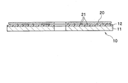
- a workpiece 10 processed by the method of the present invention includes a substrate 11 and a photoresist layer 12 provided on the surface of the substrate 11.
- This workpiece 10 shows the simplest form for understanding the invention, and other layers may be provided in addition to the substrate 11 and the photoresist layer 12.
- the workpiece 10 is a stamper used as a mold for manufacturing an optical recording disk, but is not limited thereto.
- the present invention can also be applied to a mold used for molding a product having a rough surface shape.
- the substrate 11 has a disk shape, and a through hole 11a for inserting a spindle shaft 33 described later is formed at the center.
- substrate 11 is not specifically limited, For example, Si and various metals can be used.
- the photoresist layer 12 is provided on the substrate 11 by spin coating or the like.
- the coating liquid for forming the photoresist layer 12 is generated by dissolving the compound constituting the photoresist layer 12 in an organic solvent.
- the coating material is 2% (weight ratio) of a dye material of the following chemical formula 1 in a TFP (tetrafluoropropanol) solvent which is an organic solvent. ) Can be used.
- the thickness of the photoresist layer 12 varies depending on the type of the workpiece 10, it is desirable to form the photoresist layer 12 as thin as possible when fine irregularities are to be formed on the photoresist layer 12.
- the upper limit of the film thickness is preferably 1 ⁇ m or less, more preferably 0.5 ⁇ m or less, and particularly preferably 0.3 ⁇ m or less.
- the lower limit of the film thickness of the photoresist layer 12 is desirably 0.01 ⁇ m or more, more desirably 0.03 ⁇ m or more, and particularly desirably 0.05 ⁇ m or more.
- a transparent sheet 20 is provided as an example of an object that can transmit light emitted from the exposure apparatus.
- the transparent sheet 20 has substantially the same disk shape as the work 10 in plan view, and a through hole 20a for inserting a spindle shaft 33 described later is formed at the center.
- the upper limit of the thickness of the transparent sheet 20 is desirably 80% or less, more desirably 60% or less, and further desirably 50% of the distance between the objective lens 35a and the photoresist layer 12 described later. It is as follows. This is because if it is too thick, the exposure head 35 frequently collides with the transparent sheet 20 due to variations in the position of the exposure head 35 to be described later, making control difficult.
- the lower limit of the thickness of the transparent sheet 20 is desirably 1% or more of the distance between the objective lens 35a and the photoresist layer 12, more desirably 5% or more, and further desirably 10% or more. This is because if the thickness is too thin, problems such as wrinkling occur when the transparent sheet 20 is handled.
- the position of the surface 20b (see FIG. 2) on the photoresist layer 12 side of the transparent sheet 20 is located in a region on the photoresist layer 12 side from an intermediate position between the surface of the objective lens 35a and the surface of the photoresist layer 12. It is desirable to do. More preferably, the surface 20b is in a region within 30% of the distance L1 from the photoresist layer 12 and further within 20% of the distance L1, where L1 is the distance between the objective lens 35a and the photoresist layer 12 shown in FIG. It is desirable to be located.
- the position of the surface 20b of the transparent sheet 20 is preferably within an area within 0.5 mm from the surface of the photoresist layer 12, and more preferably within an area within 0.3 mm.
- the area within 0.1 mm is most desirable.
- the transparent sheet 20 only needs to be able to transmit light emitted from the exposure apparatus to the extent that the exposure by the exposure apparatus 30 is not hindered.
- the transmittance of the laser light emitted from the laser light source is 50% or more. It is 70% or more, and more desirably 80% or more. This is because if the transmittance of the laser beam is low, the exposure efficiency of the photoresist layer 12 is poor, it takes time, and the heat generation amount of the transparent sheet 20 increases.
- the material of the transparent sheet 20 is not limited as long as it has such light transmittance.
- PC polycarbonate
- olefin triacetyl cellulose
- PET polyethylene terephthalate
- glass SiO 2 and the like
- PC polycarbonate
- olefin triacetyl cellulose
- PET polyethylene terephthalate
- SiO 2 and the like can be employed.
- PC, olefin, and TAC are preferably used.
- the transparent sheet 20 preferably has low birefringence, and the phase difference is preferably 500 nm or less, more preferably 200 nm or less, and most preferably 100 nm or less.
- the thickness of the transparent sheet 20 is preferably 1.5 mm or less, more preferably 0.7 mm or less, and most preferably 0.2 mm or less.
- the exposure apparatus 30 includes a fixed stage 31, a rotary stage 32, a spindle shaft 33, a clamp 34, an exposure head 35, and a guide 36.
- the rotary stage 32 is provided on the fixed stage 31 so as to rotate integrally with the spindle shaft 33 and the clamp 34, and a rotational driving force is input by a motor (not shown).
- the spindle shaft 33 is formed on a shaft thinner than the rotary stage 32 and is inserted into the through hole 11 a of the workpiece 10 and the through hole 20 a of the transparent sheet 20.
- the clamp 34 is provided on the top of the spindle shaft 33 and is urged downward by screws or springs. For this reason, the workpiece 10 is sandwiched between the rotary stage 32 and the clamp 34.
- the transparent sheet 20 is pressed against the workpiece 10 by the clamp 34 and is fixed to the workpiece 10.
- the air layer between the photoresist layer 12 and the transparent sheet 20 in contact with the photoresist layer 12 is exaggerated, but the transparent sheet 20 is attached to the substrate 11 by a clamp 34.
- the inner peripheral portion of the pressed transparent sheet 20 comes into close contact with the photoresist layer 12.
- the exposure head 35 can be the same as an optical pickup device used in an optical disk reading device such as a CD, DVD, or Blu-ray (registered trademark) disk.
- the exposure head 35 includes an objective lens 35a, a scanning device 35b, a focus actuator 35c, and a laser light source (not shown).
- the objective lens 35a is moved in the optical axis direction by the focus actuator 35c, and focuses the laser light emitted from the laser light source on the photoresist layer 12.
- the guide 36 is provided along the radial direction of the workpiece 10, and the scanning device 35 b moves the exposure head 35 along the guide 36.
- the wavelength of the laser light emitted from the laser light source is preferably 405 nm or 660 nm, and most preferably 405 nm.
- the exposure apparatus 30 as described above exposes the photoresist layer 12 by emitting laser light from a laser light source while rotating the work stage 10 by rotating the rotary stage 32 by a control device (not shown).
- the control device controls the focus actuator 35 c to focus the laser beam on the photoresist layer 12.
- the control device controls the scanning device 35b to move the exposure device 30 from the inner peripheral side of the workpiece 10 to the outer peripheral side or from the outer peripheral side to the inner peripheral side, thereby exposing the entire surface of the photoresist layer 12. be able to.
- the photoresist layer 12 When the photoresist layer 12 is exposed by the exposure device 30, as shown in FIG. 2, a portion of the photoresist layer 12 irradiated with the laser beam LB absorbs the laser beam LB and becomes a high temperature. Is scattered due to vaporization, sublimation or decomposition, and the shape of the photoresist layer 12 is changed to form the recess 41.
- the photoresist layer 12 since the photoresist layer 12 is a material capable of changing the shape of the heat mode, the concave portion 41 is formed only in the portion where the temperature is high. That is, it is possible to form the recess 41 that is thinner than the beam diameter and has a very narrow width.
- the scattered material 42 of a photoresist material adheres to the surface of the transparent sheet 20 which faces. Therefore, since the scattered material 42 of the photoresist material does not adhere to the objective lens 35a, the frequency of cleaning the objective lens 35a can be reduced. Therefore, production efficiency can be improved.
- the transparent sheet 20 is in contact with the photoresist layer 12, no unnecessary airflow is generated between the photoresist layer 12 and the transparent sheet 20, and the scattered photoresist material is It adheres to the transparent sheet 20 without being flowed by such an air flow. Therefore, the photoresist layer 12 is prevented from being contaminated by the scattered photoresist material.
- the objective lens 35a is finely moved in the optical axis direction by the focus actuator 35c, even if the objective lens 35a comes into contact with the transparent sheet 20 by a focus operation or external vibration, according to the processing method of this embodiment.
- the photoresist layer 12 is hardly scratched.
- the transparent sheet 20 is in contact with the photoresist layer 12 and is fixed to the substrate 11 by the clamp 34, the relative speed between the transparent sheet 20 and the photoresist layer 12 is 0 even during exposure, and the objective The possibility that the photoresist layer 12 is damaged when the lens 35a collides with the transparent sheet 20 is very low.
- the workpiece 10 having the concavo-convex shape formed on the photoresist layer 12 can make the concavo-convex shape on the substrate 11 by, for example, the process shown in FIG.
- a recess 41 is formed in the photoresist layer 12 to partially expose the surface of the substrate 11 from the photoresist layer 12, and then transparent as shown in FIG.
- the sheet 20 is peeled off from the photoresist layer 12.
- etching is performed using the photoresist layer 12 as a mask to form a recess 43 on the surface of the substrate 11.
- various etching methods such as wet etching, dry etching, and RIE (reactive ion etching) can be employed as the etching.
- corrugated pattern by the recessed part 43 can be completed on the surface of the board
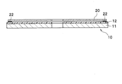
- exposure may be performed after a fine powder 21 is interposed between the photoresist layer 12 and the transparent sheet 20.
- the occurrence of an interference pattern due to the close proximity of the transparent sheet 20 and the photoresist layer 12 is prevented, and the exposure of the laser beam LB by the exposure device 30 and appropriate exposure are appropriately performed. Can be done.
- the average particle diameter is preferably 100 ⁇ m or less, more preferably 30 ⁇ m or less, and most preferably 10 ⁇ m or less.
- the average particle size is preferably 0.01 ⁇ m or more, more preferably 0.1 ⁇ m or more, and most preferably 0.5 ⁇ m or more. This is because if the particle size is too large, the focusing servo is not stabilized due to the presence of the powder 21, while if the particle size is too small, it is difficult to obtain the effect of preventing the occurrence of interference patterns, and the focusing servo is not stable.
- the average particle diameter as used in the field of this invention means the value measured by the laser diffraction method.
- the ratio of the powder 21 arranged in a certain area in the surface of the photoresist layer 12 is preferably 1% or less, more preferably 0.1% so that the powder 21 does not affect the exposure. It is desirable to disperse so that it becomes less than%, most preferably less than 0.01%.
- the transparent sheet 20 may be bonded to the workpiece 10 by the adhesive 22 only in the vicinity of the outer periphery.
- work 10 can be prevented reliably, and damage to a photoresist layer can be prevented more reliably.
- the transparent sheet 20 can be peeled without damaging the processed surface, so that a strong material can be used as the adhesive 22. I do not care.
- the method of adhering the transparent sheet 20 to the workpiece 10 may be any method that can be separated without damaging the processed surface of the photoresist layer 12. For example, an adhesive having excellent peelability from the photoresist layer 12. , The transparent sheet 20 may be adhered to the workpiece 10 over the entire surface.
- the photoresist layer 12 capable of changing the shape in the heat mode is used.
- the photoresist layer 12 that does not change the shape may be used.
- the photoresist layer 12 is exposed. Damage can be prevented. Therefore, the product yield can be improved.
- the objective lens 35a can be brought close to the photoresist layer 12, the objective lens 35a having a large NA can be used for exposure with a very small beam diameter.
- the plate-like workpiece 10 is exemplified, but the workpiece 10 is not limited to a plate-like one, and may be any shape such as a columnar shape, a cylindrical shape, or a spherical shape. Also, in the case of a plate shape, a square card shape or the like is not limited to a disk shape.
- laser light is used as light emitted from the exposure apparatus 30, but it is not necessarily required to be laser light. That is, a non-monochromatic light source can be used as long as it can be focused to a desired size.
- the clamp 34 that presses the transparent sheet 20 toward the substrate 11 is illustrated for holding the workpiece 10, but a simple chuck used for holding a CD or DVD may be used.
- the entire surface of the photoresist layer 12 is exposed by moving the workpiece 10, but the entire surface of the photoresist layer 12 is exposed by moving the exposure head 35 while the workpiece 10 is stationary. It may be.
- the material represented by Chemical Formula 1 is exemplified as the pigment material to be included in the coating solution, but the present invention is not limited to this.
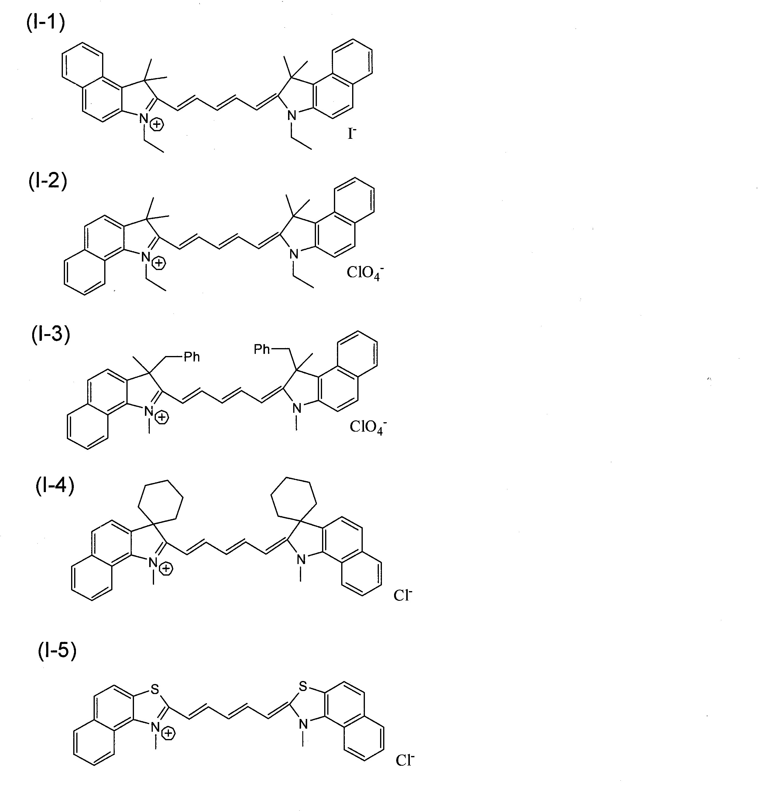
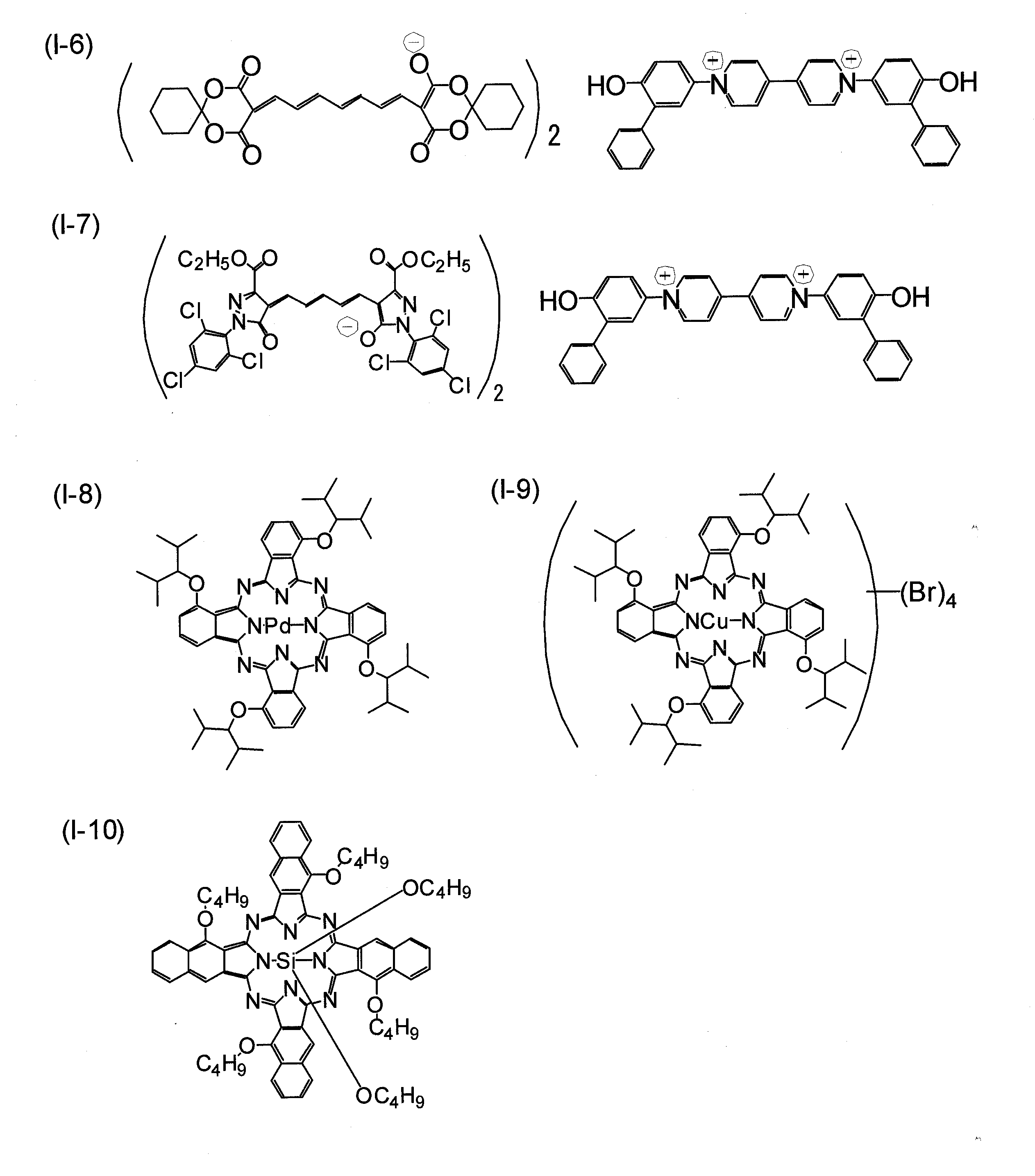
- preferable examples of the photoresist layer 12 having a dye material include methine dyes (cyanine dyes, hemicyanine dyes, styryl dyes, oxonol dyes, merocyanine dyes), macrocyclic dyes (phthalocyanine dyes, naphthalocyanine dyes, porphyrin dyes).
- Azo dyes include azo metal chelate dyes), arylidene dyes, complex dyes, coumarin dyes, azole derivatives, triazine derivatives, 1-aminobutadiene derivatives, cinnamic acid derivatives, quinophthalone dyes, and the like.
- methine dyes, oxonol dyes, macrocyclic dyes, and azo dyes are preferable.
- the dye-type photoresist layer 12 preferably contains a dye having absorption in the exposure wavelength region.
- the upper limit of the extinction coefficient k indicating the amount of light absorption is preferably 10 or less, more preferably 5 or less, further preferably 3 or less, and 1 or less. Most preferred. The reason is that if the extinction coefficient k is too high, light does not reach from the light incident side of the photoresist layer 12 to the opposite side, and uneven holes are formed.
- the lower limit value of the extinction coefficient k is preferably 0.0001 or more, more preferably 0.001 or more, and further preferably 0.1 or more. The reason is that if the extinction coefficient k is too low, the amount of light absorption is reduced, so that a larger laser power is required and the processing speed is reduced.
- the photoresist layer 12 needs to absorb light at the exposure wavelength. From such a viewpoint, a dye can be appropriately selected or the structure can be modified according to the wavelength of the laser light source.
- the oscillation wavelength of the laser light source is around 780 nm
- pentamethine cyanine dye heptamethine oxonol dye
- pentamethine oxonol dye phthalocyanine dye
- naphthalocyanine dye naphthalocyanine dye
- the oscillation wavelength of the laser light source is around 660 nm, it is advantageous to select from trimethine cyanine dye, pentamethine oxonol dye, azo dye, azo metal complex dye, pyromethene complex dye, and the like.
- a monomethine cyanine dye when the oscillation wavelength of the laser light source is around 405 nm, a monomethine cyanine dye, monomethine oxonol dye, zero methine merocyanine dye, phthalocyanine dye, azo dye, azo metal complex dye, porphyrin dye, arylidene dye, complex It is advantageous to select from dyes, coumarin dyes, azole derivatives, triazine derivatives, benzotriazole derivatives, 1-aminobutadiene derivatives, quinophthalone dyes, and the like.
- examples of preferable compounds as the photoresist layer 12 are given for the case where the oscillation wavelength of the laser light source is around 780 nm, around 660 nm, and around 405 nm, respectively.
- the compounds (I-1 to I-10) represented by the following chemical formulas 2 and 3 are compounds when the oscillation wavelength of the laser light source is around 780 nm.
- the compounds (II-1 to II-8) represented by the chemical formulas 4 and 5 are compounds when the wavelength is around 660 nm.
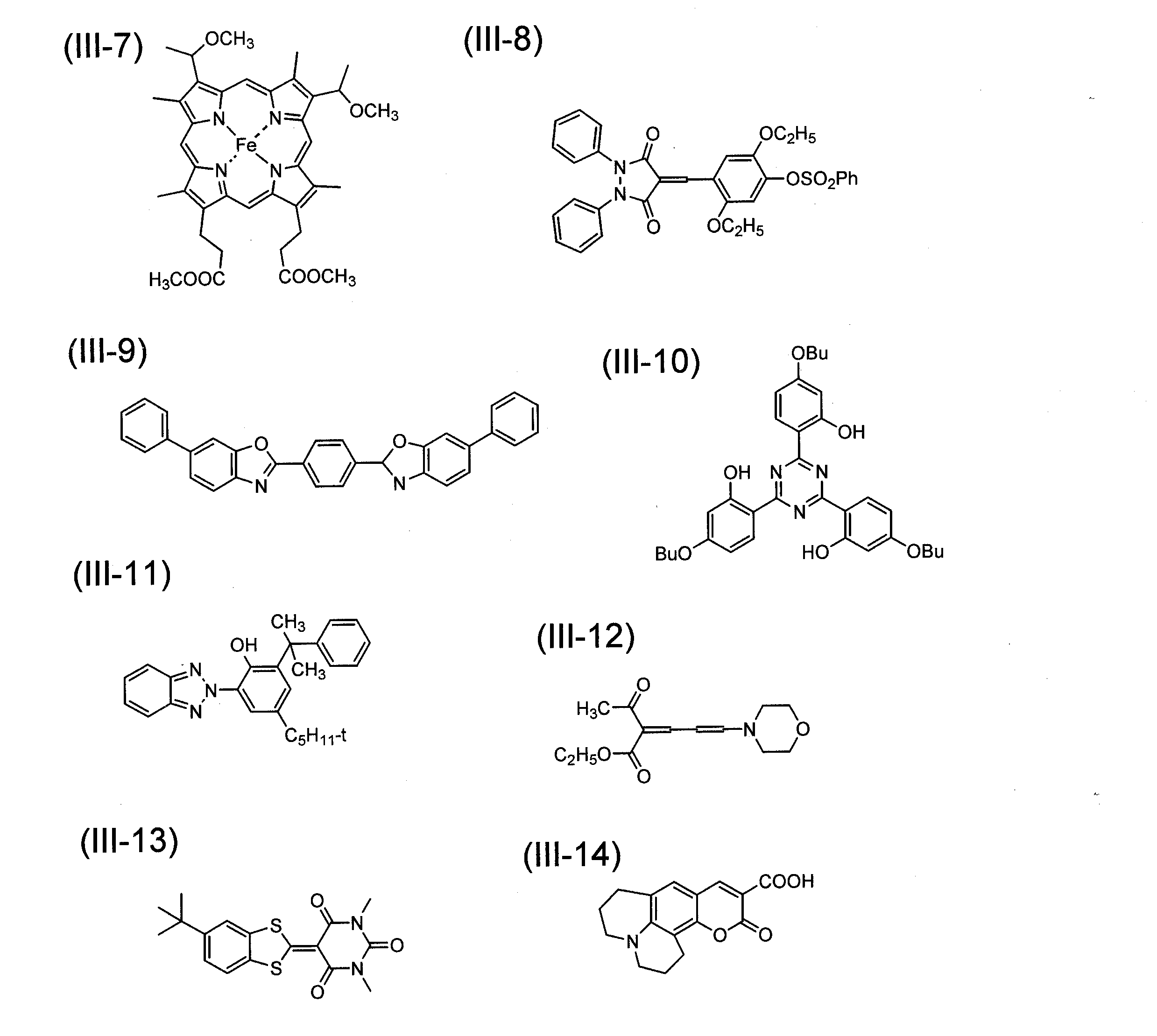
- the compounds (III-1 to III-14) represented by the chemical formulas 6 and 7 are compounds when the wavelength is around 405 nm.
- this invention is not limited to the case where these are used for a photoresist material.
- JP-A-4-74690 JP-A-8-127174, JP-A-11-53758, JP-A-11-334204, JP-A-11-334205, JP-A-11-334206,
- the dyes described in JP-A-11-334207, JP-A-2000-43423, JP-A-2000-108513, JP-A-2000-158818, and the like are also preferably used.
- Such a dye-type photoresist layer 12 is prepared by dissolving the dye in a suitable solvent together with a binder or the like to prepare a coating solution, and then coating the coating solution on the substrate 11 to form a coating film. Then, it can be formed by drying.
- the temperature of the surface on which the coating solution is applied is preferably in the range of 10 to 40 ° C. More preferably, the lower limit is 15 ° C. or higher, more preferably 20 ° C. or higher, and particularly preferably 23 ° C. or higher.
- the upper limit it is more preferable that it is 35 degrees C or less, It is still more preferable that it is 30 degrees C or less, It is especially preferable that it is 27 degrees C or less.
- the photoresist layer 12 may be a single layer or a multilayer. In the case of a multilayer structure, the photoresist layer 12 is formed by performing the coating process a plurality of times.
- the concentration of the dye in the coating solution is generally in the range of 0.01 to 15% by mass, preferably in the range of 0.1 to 10% by mass, more preferably in the range of 0.5 to 5% by mass, and most preferably. It is in the range of 0.5 to 3% by mass.
- Examples of the solvent for the coating solution include esters such as butyl acetate, ethyl lactate and cellosolve acetate; ketones such as methyl ethyl ketone, cyclohexanone and methyl isobutyl ketone; chlorinated hydrocarbons such as dichloromethane, 1,2-dichloroethane and chloroform; dimethylformamide and the like Amides; Hydrocarbons such as methylcyclohexane; Ethers such as tetrahydrofuran, ethyl ether and dioxane; Alcohols such as ethanol, n-propanol, isopropanol, n-butanol diacetone alcohol; 2,2,3,3-tetrafluoropropanol and the like Fluorinated solvents; glycol ethers such as ethylene glycol monomethyl ether, ethylene glycol monoethyl ether, propylene glycol monomethyl ether; That.
- esters such
- Fluorine solvents, glycol ethers, and ketones are preferred. Particularly preferred are fluorine type solvents and glycol ethers. More preferred are 2,2,3,3-tetrafluoropropanol and propylene glycol monomethyl ether.
- the said solvent can be used individually or in combination of 2 or more types in consideration of the solubility of the pigment
- various additives such as an antioxidant, a UV absorber, a plasticizer, and a lubricant may be added according to the purpose.
- the temperature of the coating solution is preferably in the range of 23 to 50 ° C., more preferably in the range of 24 to 40 ° C., and particularly in the range of 25 to 30 ° C. preferable.
- the binder include natural organic polymer materials such as gelatin, cellulose derivatives, dextran, rosin, and rubber; hydrocarbon resins such as polyethylene, polypropylene, polystyrene, and polyisobutylene; Vinyl resins such as polyvinyl chloride, polyvinylidene chloride, polyvinyl chloride / polyvinyl acetate copolymer, acrylic resins such as polymethyl acrylate and polymethyl methacrylate, polyvinyl alcohol, chlorinated polyethylene, epoxy resin, butyral resin And synthetic organic polymers such as initial condensation products of thermosetting resins such as rubber derivatives and phenol / formaldehyde resins.
- natural organic polymer materials such as gelatin, cellulose derivatives, dextran, rosin, and rubber
- hydrocarbon resins such as polyethylene, polypropylene, polystyrene, and polyisobutylene
- Vinyl resins such as polyvinyl chloride, polyvinylidene chloride, polyvinyl
- the amount of the binder used is generally in the range of 0.01 to 50 times (mass ratio) with respect to the dye, preferably 0.1. It is in the range of double to 5 times (mass ratio).
- the photoresist layer 12 can contain various anti-fading agents in order to improve the light resistance of the photoresist layer 12.
- a singlet oxygen quencher is generally used.
- the singlet oxygen quencher those described in publications such as known patent specifications can be used. Specific examples thereof include JP-A-58-175893, JP-A-59-81194, JP-A-60-18387, JP-A-60-19586, and JP-A-60-19587.
- the amount of the anti-fading agent such as the singlet oxygen quencher used is usually in the range of 0.1 to 50% by weight, preferably in the range of 0.5 to 45% by weight, based on the amount of the dye.
- the range is preferably 3 to 40% by mass, particularly preferably 5 to 25% by mass.
- the wavelength of the absorption peak of the dye is not necessarily limited to that in the visible light wavelength range, and may be in the ultraviolet range or the infrared range.
- the wavelength ⁇ w for forming the pattern of the concave portion 41 with a laser is preferably in the relationship of ⁇ a ⁇ w in relation to the dye absorption wavelength ⁇ a. With such a relationship, the light absorption amount of the dye is appropriate, the formation efficiency is increased, and a clean uneven shape can be formed.
- the wavelength ⁇ w of the laser light for forming the concave pattern 51 may be any wavelength that can obtain a large laser power.
- 193 nm, 210 nm, 266 nm, 365 nm, 405 nm, 488 nm, 532 nm, 633 nm, 650 nm, 680 nm , 780 nm, 830 nm and the like are preferably 1000 nm or less.
- the laser beam may be any laser such as a gas laser, a solid laser, or a semiconductor laser.
- a solid-state laser or a semiconductor laser in order to simplify the optical system, it is preferable to employ a solid-state laser or a semiconductor laser.
- the laser light may be continuous light or pulsed light, but it is preferable to employ laser light whose emission interval can be freely changed.
- the laser cannot be directly on / off modulated, it is preferable to modulate with an external modulation element.
- the laser power is high in order to increase the processing speed.
- the scanning speed speed at which the photoresist layer 12 is scanned with laser light
- the upper limit value of the laser power is preferably 100 W in consideration of the upper limit value of the scanning speed, more preferably 10 W, still more preferably 5 W, and most preferably 1 W.
- the lower limit of the laser power is preferably 0.1 mW, more preferably 0.5 mW, and even more preferably 1 mW.
- the laser light is preferably light that has excellent transmission wavelength width and coherency and can be narrowed down to a spot size comparable to the wavelength.
- the exposure strategy (light pulse irradiation conditions for properly forming the pattern of the recesses 41), it is preferable to adopt a strategy used in an optical disc. That is, it is preferable to adopt conditions such as the exposure speed, the peak value of the laser beam to be irradiated, and the pulse width as used in optical disks.
- the vaporization, sublimation or decomposition of the photoresist layer 12 preferably has a large rate of change and is steep.
- the weight reduction rate by differential thermal balance (TG-DTA) at the time of vaporization, sublimation or decomposition of the photoresist layer 12 is preferably 5% or more, more preferably 10% or more, still more preferably 20 % Or more.
- the slope of weight reduction (weight reduction rate per 1 ° C. temperature increase) by the differential thermal balance (TG-DTA) at the time of vaporization, sublimation or decomposition of the photoresist layer 12 is 0.1% / ° C. or more. Preferably, it is 0.2% / ° C. or more, more preferably 0.4% / ° C. or more.
- the transition temperature of chemical or / and physical change such as softening, liquefaction, vaporization, sublimation, decomposition, etc. is preferably 2000 ° C. or less, more preferably 1000 ° C. or less, more preferably 500 ° C. More preferably, it is as follows. The reason is that if the transition temperature is too high, a large laser power is required.
- the lower limit of the transition temperature is preferably 50 ° C. or higher, more preferably 100 ° C. or higher, and further preferably 150 ° C. or higher. The reason is that if the transition temperature is too low, the temperature gradient from the surroundings is small, and a clear hole edge shape cannot be formed.
- a disk-shaped substrate was prepared, and a 100 nm thick photoresist layer was formed on the substrate. Then, a polycarbonate film having a thickness of 0.1 mm was placed as a transparent sheet on the photoresist layer, and the photoresist layer was exposed through the polycarbonate film. The substrate and polycarbonate film chucked the inner periphery of the central hole. Details of each member are as follows.
- Dye layer (photoresist layer) 2 g of the dye material of the above chemical formula 1 was dissolved in 100 ml of a TFP (tetrafluoropropanol) solvent and spin-coated. At the time of spin coating, the coating liquid was dispensed on the inner periphery of the substrate at a coating start rotation speed of 500 rpm and a coating end rotation speed of 1000 rpm, and the rotation was gradually increased to 2200 rpm.
- the refractive index n of the dye material is 1.986, and the extinction coefficient k is 0.0418.
- fine concave portions were formed from the surface on the photoresist layer side with DDU1000 (wavelength 405 nm, NA 0.85) manufactured by Pulstec Industrial Co., Ltd.
- the concave portions were formed in a spiral shape with a width of 0.2 ⁇ m and a pitch of 0.5 ⁇ m.
- the conditions for forming the recess are as follows. Laser power 2mW Line speed 5m / s Exposure signal 5 MHz rectangular wave
- the concave portions could be formed satisfactorily in the photoresist layer.
- the objective lens was carefully observed, but no scattered material of the photoresist material was found. Thereafter, dry etching was successfully performed using this photoresist layer as a mask.
- Example 2 SiO 2 powder having an average particle diameter of 1 ⁇ m was sparsely disposed between the photoresist layer and the polycarbonate film, and the polycarbonate film was fixed to the substrate with a chuck.
- the other test pieces were the same as in Example 1.
- the polycarbonate film of this test piece was locally pressed against the photoresist layer with a finger, no interference pattern was generated.
- the photoresist layer was exposed under the same conditions as in Example 1, no problem occurred in focusing, and concave portions could be formed satisfactorily in the photoresist layer.
- dry etching could be performed under the same conditions as in Example 1.
- Example 1 A test piece with the polycarbonate film removed was prepared for the test piece of Example 1, and the photoresist layer was exposed under the same conditions as in Example 1. The optical system was changed so that the photoresist layer was in focus. When the objective lens was carefully observed after the exposure, a slight amount of scattered photoresist was observed.
- Example 2 In the test piece of Example 1, the polycarbonate film was locally pressed against the photoresist layer with a finger. As a result, an interference pattern was observed. When the photoresist layer was exposed under the same conditions as in Example 1 with this interference pattern being generated, the focus of the exposure apparatus was not stable, and a recess could not be formed in the photoresist layer.
Landscapes
- Engineering & Computer Science (AREA)
- Physics & Mathematics (AREA)
- Chemical & Material Sciences (AREA)
- Nanotechnology (AREA)
- General Physics & Mathematics (AREA)
- Manufacturing & Machinery (AREA)
- Crystallography & Structural Chemistry (AREA)
- Optics & Photonics (AREA)
- Condensed Matter Physics & Semiconductors (AREA)
- Mathematical Physics (AREA)
- Theoretical Computer Science (AREA)
- Plasma & Fusion (AREA)
- Exposure And Positioning Against Photoresist Photosensitive Materials (AREA)
- Exposure Of Semiconductors, Excluding Electron Or Ion Beam Exposure (AREA)
Abstract
Description
これにより、ワークに露光パターンに応じた凹凸形状を形成することができる。
物体とフォトレジスト層を接触させる場合、前記したように、通常これらの間に不可避的に空気層が介在しうるが、物体がフォトレジスト層に部分的に近づくと、その場所に光の干渉模様、いわゆるニュートンリングが発生する。このような干渉模様があると、露光時のフォーカシングに影響を与える可能性があるが、粉体を介在させることで、物体とフォトレジスト層との間に所定の微小な隙間を確保でき、干渉模様の発生を防止することができる。
これにより、物体とワークとの相対移動を確実に防止でき、フォトレジスト層の損傷をより確実に防止できる。

回転ステージ32は、固定ステージ31上において、スピンドル軸33およびクランプ34と一体で回転するように設けられ、図示しないモータにより回転駆動力が入力される。
スピンドル軸33は、回転ステージ32より細い軸に形成され、ワーク10の貫通孔11aおよび透明シート20の貫通孔20aに挿通される。
クランプ34は、スピンドル軸33の頂部に設けられ、ネジ止めまたはバネにより下側に付勢されている。このため、ワーク10は、回転ステージ32とクランプ34との間で挟持されている。つまり、透明シート20は、クランプ34によりワーク10に押し付けられ、ワーク10に固定されている。なお、添付した各図面においては、フォトレジスト層12と、これに接触している透明シート20との間の空気層を誇張して表現してあるが、クランプ34で透明シート20を基板11に向けて押し付けると、その押し付けられた透明シート20の内周部はフォトレジスト層12に密着する。
露光ヘッド35は、対物レンズ35a、スキャン装置35b、フォーカスアクチュエータ35cおよび図示しないレーザ光源を有する。対物レンズ35aは、フォーカスアクチュエータ35cにより光軸方向に移動され、フォトレジスト層12上に、レーザ光源から出射したレーザ光を集束させるようになっている。ガイド36は、ワーク10の径方向に沿って設けられ、スキャン装置35bは、ガイド36に沿って露光ヘッド35を移動させるようになっている。
なお、レーザ光源が発するレーザ光の波長は、405nmや660nmが好ましく、405nmが最も好ましい。
また、本実施形態においては、透明シート20は、フォトレジスト層12に接触しているので、フォトレジスト層12と透明シート20の間で不要な気流は発生せず、飛散したフォトレジスト材料は、かかる気流に流されることなく、透明シート20に付着する。そのため、飛散したフォトレジスト材料によりフォトレジスト層12が汚れることが抑制される。
例えば、図4に示すように、フォトレジスト層12と透明シート20との間に微小な粉体21を介在させた上で露光を行ってもよい。このように、粉体21を介在させることで、透明シート20とフォトレジスト層12が局部的に近づくことによる干渉模様の発生を防止し、露光装置30によるレーザ光LBのフォーカシングや、露光を適切に行うことができる。
なお、本発明にいう平均粒径とは、レーザ回折法により測定された値をいう。


なお、上記の上限値及び下限値は、それぞれが任意で組み合わせることができる。
ここで、フォトレジスト層12は、単層でも重層でもよく、重層構造の場合、塗布工程を複数回行うことによって形成される。
塗布液中の色素の濃度は、一般に0.01~15質量%の範囲であり、好ましくは0.1~10質量%の範囲、より好ましくは0.5~5質量%の範囲、最も好ましくは0.5~3質量%の範囲である。
上記溶剤は使用する色素の溶解性を考慮して単独で、或いは二種以上を組み合わせて使用することができる。塗布液中には、更に、酸化防止剤、UV吸収剤、可塑剤、潤滑剤等各種の添加剤を目的に応じて添加してもよい。
褪色防止剤としては、一般的に一重項酸素クエンチャーが用いられる。一重項酸素クエンチャーとしては、既に公知の特許明細書等の刊行物に記載のものを利用することができる。
その具体例としては、特開昭58-175693号公報、特開昭59-81194号公報、特開昭60-18387号公報、特開昭60-19586号公報、特開昭60-19587号公報、特開昭60-35054号公報、特開昭60-36190号公報、特開昭60-36191号公報、特開昭60-44554号公報、特開昭60-44555号公報、特開昭60-44389号公報、特開昭60-44390号公報、特開昭60-54892号公報、特開昭60-47069号公報、特開昭63-209995号公報、特開平4-25492号公報、特公平1-38680号公報、及び特公平6-26028号公報等の各公報、ドイツ特許350399号明細書、そして日本化学会誌1992年10月号第1141頁等に記載のものを挙げることができる。前記一重項酸素クエンチャー等の褪色防止剤の使用量は、色素の量に対して、通常0.1~50質量%の範囲であり、好ましくは、0.5~45質量%の範囲、更に好ましくは、3~40質量%の範囲、特に好ましくは5~25質量%の範囲である。
上述した実施形態と同様に、円板形状の基板を用意し、この基板上に100nm厚のフォトレジスト層を形成した。そして、フォトレジスト層の上に透明シートとして0.1mm厚のポリカーボネートフィルムを接触させて配置して、ポリカーボネートフィルムを通してフォトレジスト層を露光した。基板およびポリカーボネートフィルムは、中央の孔の内周をチャックした。
各部材の詳細は以下の通りである。
材質 シリコン
厚さ 0.6mm
外径 10.2cm(4インチ)
内径 15mm
前記した化学式1の色素材料2gをTFP(テトラフルオロプロパノール)溶剤100mlに溶解し、スピンコートした。スピンコートの際には、塗布開始回転数500rpm、塗布終了回転数1000rpmとして塗布液を基板の内周部にディスペンスし、徐々に2200rpmまで回転を上げた。なお、色素材料の屈折率nは1.986であり、消衰係数kは0.0418である。
凹部の形成条件は下記の通りである。
レーザ出力 2mW
線速 5m/s
露光信号 5MHzの矩形波
エッチングガス SF6+CHF3(1:1)
凹部の深さ 50nm
フォトレジスト層を剥離する剥離液 エタノール
フォトレジスト層とポリカーボネートフィルムの間に平均粒径1μmのSiO2粉体をまばらに配置し、ポリカーボネートフィルムをチャックで基板に固定した。その他は、実施例1と同様のテストピースとした。
このテストピースのポリカーボネートフィルムを指で局部的にフォトレジスト層に押し付けたところ、干渉模様は発生しなかった。
そして、実施例1と同じ条件でフォトレジスト層の露光を行ったところ、フォーカシングに問題は生じず、フォトレジスト層に良好に凹部を形成することができた。そして、このフォトレジスト層をマスクとして実施例1と同じ条件でドライエッチングを行うことができた。
実施例1のテストピースに対し、ポリカーボネートフィルムを外した状態のテストピースを用意し、実施例1と同じ条件でフォトレジスト層の露光を行った。なお、フォトレジスト層にフォーカスが合うように、光学系を変更した。
露光後、対物レンズを注意深く観察すると、フォトレジストの飛散物が僅かに観察された。
実施例1のテストピースにおいて、ポリカーボネートフィルムを指で局部的にフォトレジスト層に押し付けた。その結果、干渉模様が観察された。
この干渉模様が発生したまま、実施例1と同じ条件でフォトレジスト層の露光を行ったところ、露光装置のフォーカスが安定せず、フォトレジスト層に凹部を形成することができなかった。
Claims (11)
- 露光装置を用いてフォトレジスト層を有するワークを加工する加工方法であって、
前記露光装置の対物レンズと前記フォトレジスト層との間に、前記露光装置が発する光を透過可能な物体を配置し、当該物体を通して前記フォトレジスト層を露光することを特徴とする加工方法。 - 前記フォトレジスト層は、ヒートモード型の形状変化が可能な材料からなることを特徴とする請求の範囲第1項に記載の加工方法。
- フォトレジスト層の露光後、前記フォトレジスト層をマスクとして前記ワークをエッチングすることを特徴とする請求の範囲第1項に記載の加工方法。
- 前記物体を前記フォトレジスト層に接触させて配置し、前記露光を行うことを特徴とする請求の範囲第1項に記載の加工方法。
- 前記フォトレジスト層と前記物体との間に粉体を介在させることを特徴とする請求の範囲第4項に記載の加工方法。
- 前記粉体の大きさは、平均粒径が0.01~100μmであることを特徴とする請求の範囲第5項に記載の加工方法。
- 前記露光時において、前記ワークを回転させながら露光を行うことを特徴とする請求の範囲第1項に記載の加工方法。
- 前記露光時において、前記物体を前記ワークにクランプにより固定することを特徴とする請求の範囲第7項に記載の加工方法。
- 前記露光時において、前記フォトレジスト層の被加工面から分離可能な方法で前記物体を前記ワークに接着しておくことを特徴とする請求の範囲第7項に記載の加工方法。
- 前記物体は、シート状であることを特徴とする請求の範囲第1項に記載の加工方法。
- 前記シート状の物体は、厚さが、前記対物レンズと前記フォトレジスト層との距離の1~80%であることを特徴とする請求の範囲第10項に記載の加工方法。
Priority Applications (3)
| Application Number | Priority Date | Filing Date | Title |
|---|---|---|---|
| CN2008801277739A CN101960383B (zh) | 2008-03-05 | 2008-12-15 | 用于加工具有光致抗蚀剂层的工件的方法 |
| US12/921,116 US8309296B2 (en) | 2008-03-05 | 2008-12-15 | Method for processing workpiece with photoresist layer |
| EP20080873154 EP2264527A4 (en) | 2008-03-05 | 2008-12-15 | Method for processing work having photoresist layer |
Applications Claiming Priority (2)
| Application Number | Priority Date | Filing Date | Title |
|---|---|---|---|
| JP2008-055611 | 2008-03-05 | ||
| JP2008055611A JP4950101B2 (ja) | 2008-03-05 | 2008-03-05 | フォトレジスト層を有するワークの加工方法 |
Publications (1)
| Publication Number | Publication Date |
|---|---|
| WO2009110046A1 true WO2009110046A1 (ja) | 2009-09-11 |
Family
ID=41055628
Family Applications (1)
| Application Number | Title | Priority Date | Filing Date |
|---|---|---|---|
| PCT/JP2008/003762 Ceased WO2009110046A1 (ja) | 2008-03-05 | 2008-12-15 | フォトレジスト層を有するワークの加工方法 |
Country Status (7)
| Country | Link |
|---|---|
| US (1) | US8309296B2 (ja) |
| EP (1) | EP2264527A4 (ja) |
| JP (1) | JP4950101B2 (ja) |
| KR (1) | KR20100124724A (ja) |
| CN (1) | CN101960383B (ja) |
| TW (1) | TW200938953A (ja) |
| WO (1) | WO2009110046A1 (ja) |
Families Citing this family (2)
| Publication number | Priority date | Publication date | Assignee | Title |
|---|---|---|---|---|
| CN102073225B (zh) * | 2011-02-14 | 2012-10-03 | 中国科学院光电技术研究所 | 一种纳光子直写头精密旋转定位调焦系统 |
| CN102184881B (zh) * | 2011-04-01 | 2012-08-15 | 百力达太阳能股份有限公司 | 一种硅片干法刻蚀前的整理方法 |
Citations (42)
| Publication number | Priority date | Publication date | Assignee | Title |
|---|---|---|---|---|
| DE350399C (de) | 1919-09-19 | 1922-03-20 | Qu Bernd Ziemert | Projektionsschirm |
| JPS58175693A (ja) | 1982-04-08 | 1983-10-14 | Ricoh Co Ltd | 高密度光情報記録媒体 |
| JPS5981194A (ja) | 1982-11-01 | 1984-05-10 | Tdk Corp | 光記録媒体 |
| JPS6018387A (ja) | 1983-07-11 | 1985-01-30 | Tdk Corp | 光記録媒体 |
| JPS6019586A (ja) | 1983-07-13 | 1985-01-31 | Tdk Corp | 光記録媒体 |
| JPS6019587A (ja) | 1983-07-13 | 1985-01-31 | Tdk Corp | 光記録媒体 |
| JPS6035054A (ja) | 1983-08-05 | 1985-02-22 | Tdk Corp | 光記録媒体 |
| JPS6036191A (ja) | 1983-08-09 | 1985-02-25 | Tdk Corp | 光記録媒体 |
| JPS6036190A (ja) | 1983-08-09 | 1985-02-25 | Tdk Corp | 光記録媒体 |
| JPS6044554A (ja) | 1983-08-20 | 1985-03-09 | Tdk Corp | 光記録媒体 |
| JPS6044555A (ja) | 1983-08-20 | 1985-03-09 | Tdk Corp | 光記録媒体 |
| JPS6044390A (ja) | 1983-08-23 | 1985-03-09 | Tdk Corp | 光記録媒体 |
| JPS6044389A (ja) | 1983-08-23 | 1985-03-09 | Tdk Corp | 光記録媒体 |
| JPS6047069A (ja) | 1983-08-24 | 1985-03-14 | Tdk Corp | 光記録媒体 |
| JPS6054892A (ja) | 1983-09-05 | 1985-03-29 | Tdk Corp | 光記録媒体 |
| JPS61237313A (ja) * | 1985-04-12 | 1986-10-22 | シャープ株式会社 | 薄膜タツチパネル |
| JPS63209995A (ja) | 1987-02-27 | 1988-08-31 | Fuji Photo Film Co Ltd | 光学的情報記録媒体 |
| JPH0191385A (ja) * | 1987-09-30 | 1989-04-11 | Sharp Corp | 光ディスクの製造方法 |
| JPH0138680B2 (ja) | 1982-09-27 | 1989-08-15 | Tdk Electronics Co Ltd | |
| JPH03144646A (ja) * | 1989-10-31 | 1991-06-20 | Toyobo Co Ltd | ニュートンリング防止用フイルム |
| JPH0425492A (ja) | 1990-05-21 | 1992-01-29 | Tdk Corp | 光記録媒体 |
| JPH0474690A (ja) | 1990-07-17 | 1992-03-10 | Ricoh Co Ltd | 光情報記録媒体 |
| JPH04209517A (ja) * | 1990-12-05 | 1992-07-30 | Nikon Corp | 薄膜除去方法 |
| JPH04345921A (ja) | 1991-05-22 | 1992-12-01 | Hitachi Maxell Ltd | 光ディスク記録装置 |
| JPH0626028B2 (ja) | 1984-02-06 | 1994-04-06 | 株式会社リコー | 光情報記録媒体 |
| JPH08127174A (ja) | 1994-10-31 | 1996-05-21 | Sony Corp | 光記録媒体 |
| JPH08212602A (ja) * | 1995-10-24 | 1996-08-20 | Pioneer Electron Corp | 記録媒体 |
| JPH1153758A (ja) | 1997-07-30 | 1999-02-26 | Mitsubishi Chem Corp | 記録再生方法 |
| JPH11334204A (ja) | 1998-05-27 | 1999-12-07 | Mitsubishi Chemical Corp | 光学記録媒体 |
| JPH11334206A (ja) | 1998-05-27 | 1999-12-07 | Mitsubishi Chemical Corp | 光学記録媒体 |
| JPH11334207A (ja) | 1998-05-27 | 1999-12-07 | Mitsubishi Chemical Corp | 光学記録媒体 |
| JPH11334205A (ja) | 1998-05-27 | 1999-12-07 | Mitsubishi Chemical Corp | 光学記録媒体 |
| JP2000043423A (ja) | 1998-05-27 | 2000-02-15 | Mitsubishi Chemicals Corp | 光学記録媒体 |
| JP2000108513A (ja) | 1998-10-05 | 2000-04-18 | Mitsui Chemicals Inc | 光記録媒体 |
| JP2000158818A (ja) | 1998-12-01 | 2000-06-13 | Mitsui Chemicals Inc | 光記録媒体 |
| JP2001195784A (ja) * | 2000-01-07 | 2001-07-19 | Sony Disc Technology Inc | 光記録媒体およびその製造方法 |
| JP2003066852A (ja) * | 2001-08-24 | 2003-03-05 | Sanyo Electric Co Ltd | プラズマディスプレイ装置 |
| JP2004213707A (ja) * | 2002-12-26 | 2004-07-29 | Ricoh Co Ltd | 光ディスク原盤露光装置 |
| JP2005011489A (ja) * | 2003-05-28 | 2005-01-13 | Matsushita Electric Ind Co Ltd | 光情報記録媒体の原盤製造方法 |
| JP2006309908A (ja) * | 2005-04-01 | 2006-11-09 | Hitachi Maxell Ltd | 狭トラックピッチ基板の製造方法及び製造装置、それによって得られた狭トラックピッチ基板 |
| JP2006308996A (ja) * | 2005-04-28 | 2006-11-09 | Fuji Photo Film Co Ltd | 露光装置 |
| JP2007094410A (ja) * | 2005-09-29 | 2007-04-12 | Hitachi Global Storage Technologies Netherlands Bv | パターン化された磁気記録ディスクをナノインプリントするためのマスタ・ディスクをパターン化するためのシステム及び方法 |
Family Cites Families (17)
| Publication number | Priority date | Publication date | Assignee | Title |
|---|---|---|---|---|
| US4319252A (en) * | 1980-07-21 | 1982-03-09 | Drexler Technology Corporation | Optical data storage and recording medium having a replaceable protective coverplate |
| US4897325A (en) * | 1985-11-18 | 1990-01-30 | The Perkin-Elmer Corporation | Contact lithographic fabrication of patterns on large optics |
| JPH02109743A (ja) * | 1988-10-19 | 1990-04-23 | Aisin Seiki Co Ltd | 定速走行制御装置 |
| US5656229A (en) * | 1990-02-20 | 1997-08-12 | Nikon Corporation | Method for removing a thin film layer |
| JPH04233716A (ja) * | 1990-12-28 | 1992-08-21 | Nikon Corp | 薄膜除去装置 |
| JP2753930B2 (ja) | 1992-11-27 | 1998-05-20 | キヤノン株式会社 | 液浸式投影露光装置 |
| JPH07100670A (ja) * | 1993-10-05 | 1995-04-18 | Nippon Steel Corp | レーザ加工装置 |
| DE69407620T2 (de) | 1993-12-17 | 1998-04-09 | Minnesota Mining & Mfg | Ablationsabbildung durch quasikontaktlithographie |
| JPH08124226A (ja) * | 1994-10-27 | 1996-05-17 | Sony Corp | 光ディスク製造方法及び光ディスク製造装置 |
| AU2233499A (en) * | 1998-02-13 | 1999-08-30 | Howard A. Fromson | Laser ablative lithographic printing plate with debris entrainment and process of use |
| JP3241656B2 (ja) * | 1998-02-19 | 2001-12-25 | 日本電気株式会社 | 露光装置 |
| US6136509A (en) * | 1998-06-05 | 2000-10-24 | Creo Srl | Method of exposing thermoresist |
| JP2001250280A (ja) * | 2000-03-02 | 2001-09-14 | Sony Corp | 記録媒体、記録媒体の製造方法、記録媒体製造用原盤の製造方法、記録媒体の製造装置、および記録媒体製造用原盤の製造装置 |
| WO2004053938A2 (en) * | 2002-12-09 | 2004-06-24 | Pixelligent Technologies Llc | Programmable photolithographic mask based on nano-sized semiconductor particles |
| EP1482494A3 (en) * | 2003-05-28 | 2007-08-29 | Matsushita Electric Industrial Co., Ltd. | Method for producing master for optical information recording media |
| US6906777B1 (en) * | 2004-03-01 | 2005-06-14 | Advanced Micro Devices, Inc. | Pellicle for a lithographic lens |
| TW200702940A (en) | 2005-04-28 | 2007-01-16 | Fuji Photo Film Co Ltd | Exposure apparatus |
-
2008
- 2008-03-05 JP JP2008055611A patent/JP4950101B2/ja not_active Expired - Fee Related
- 2008-12-15 CN CN2008801277739A patent/CN101960383B/zh not_active Expired - Fee Related
- 2008-12-15 EP EP20080873154 patent/EP2264527A4/en not_active Withdrawn
- 2008-12-15 WO PCT/JP2008/003762 patent/WO2009110046A1/ja not_active Ceased
- 2008-12-15 US US12/921,116 patent/US8309296B2/en not_active Expired - Fee Related
- 2008-12-15 KR KR1020107018425A patent/KR20100124724A/ko not_active Ceased
-
2009
- 2009-01-06 TW TW098100166A patent/TW200938953A/zh unknown
Patent Citations (42)
| Publication number | Priority date | Publication date | Assignee | Title |
|---|---|---|---|---|
| DE350399C (de) | 1919-09-19 | 1922-03-20 | Qu Bernd Ziemert | Projektionsschirm |
| JPS58175693A (ja) | 1982-04-08 | 1983-10-14 | Ricoh Co Ltd | 高密度光情報記録媒体 |
| JPH0138680B2 (ja) | 1982-09-27 | 1989-08-15 | Tdk Electronics Co Ltd | |
| JPS5981194A (ja) | 1982-11-01 | 1984-05-10 | Tdk Corp | 光記録媒体 |
| JPS6018387A (ja) | 1983-07-11 | 1985-01-30 | Tdk Corp | 光記録媒体 |
| JPS6019586A (ja) | 1983-07-13 | 1985-01-31 | Tdk Corp | 光記録媒体 |
| JPS6019587A (ja) | 1983-07-13 | 1985-01-31 | Tdk Corp | 光記録媒体 |
| JPS6035054A (ja) | 1983-08-05 | 1985-02-22 | Tdk Corp | 光記録媒体 |
| JPS6036191A (ja) | 1983-08-09 | 1985-02-25 | Tdk Corp | 光記録媒体 |
| JPS6036190A (ja) | 1983-08-09 | 1985-02-25 | Tdk Corp | 光記録媒体 |
| JPS6044555A (ja) | 1983-08-20 | 1985-03-09 | Tdk Corp | 光記録媒体 |
| JPS6044554A (ja) | 1983-08-20 | 1985-03-09 | Tdk Corp | 光記録媒体 |
| JPS6044390A (ja) | 1983-08-23 | 1985-03-09 | Tdk Corp | 光記録媒体 |
| JPS6044389A (ja) | 1983-08-23 | 1985-03-09 | Tdk Corp | 光記録媒体 |
| JPS6047069A (ja) | 1983-08-24 | 1985-03-14 | Tdk Corp | 光記録媒体 |
| JPS6054892A (ja) | 1983-09-05 | 1985-03-29 | Tdk Corp | 光記録媒体 |
| JPH0626028B2 (ja) | 1984-02-06 | 1994-04-06 | 株式会社リコー | 光情報記録媒体 |
| JPS61237313A (ja) * | 1985-04-12 | 1986-10-22 | シャープ株式会社 | 薄膜タツチパネル |
| JPS63209995A (ja) | 1987-02-27 | 1988-08-31 | Fuji Photo Film Co Ltd | 光学的情報記録媒体 |
| JPH0191385A (ja) * | 1987-09-30 | 1989-04-11 | Sharp Corp | 光ディスクの製造方法 |
| JPH03144646A (ja) * | 1989-10-31 | 1991-06-20 | Toyobo Co Ltd | ニュートンリング防止用フイルム |
| JPH0425492A (ja) | 1990-05-21 | 1992-01-29 | Tdk Corp | 光記録媒体 |
| JPH0474690A (ja) | 1990-07-17 | 1992-03-10 | Ricoh Co Ltd | 光情報記録媒体 |
| JPH04209517A (ja) * | 1990-12-05 | 1992-07-30 | Nikon Corp | 薄膜除去方法 |
| JPH04345921A (ja) | 1991-05-22 | 1992-12-01 | Hitachi Maxell Ltd | 光ディスク記録装置 |
| JPH08127174A (ja) | 1994-10-31 | 1996-05-21 | Sony Corp | 光記録媒体 |
| JPH08212602A (ja) * | 1995-10-24 | 1996-08-20 | Pioneer Electron Corp | 記録媒体 |
| JPH1153758A (ja) | 1997-07-30 | 1999-02-26 | Mitsubishi Chem Corp | 記録再生方法 |
| JP2000043423A (ja) | 1998-05-27 | 2000-02-15 | Mitsubishi Chemicals Corp | 光学記録媒体 |
| JPH11334206A (ja) | 1998-05-27 | 1999-12-07 | Mitsubishi Chemical Corp | 光学記録媒体 |
| JPH11334207A (ja) | 1998-05-27 | 1999-12-07 | Mitsubishi Chemical Corp | 光学記録媒体 |
| JPH11334205A (ja) | 1998-05-27 | 1999-12-07 | Mitsubishi Chemical Corp | 光学記録媒体 |
| JPH11334204A (ja) | 1998-05-27 | 1999-12-07 | Mitsubishi Chemical Corp | 光学記録媒体 |
| JP2000108513A (ja) | 1998-10-05 | 2000-04-18 | Mitsui Chemicals Inc | 光記録媒体 |
| JP2000158818A (ja) | 1998-12-01 | 2000-06-13 | Mitsui Chemicals Inc | 光記録媒体 |
| JP2001195784A (ja) * | 2000-01-07 | 2001-07-19 | Sony Disc Technology Inc | 光記録媒体およびその製造方法 |
| JP2003066852A (ja) * | 2001-08-24 | 2003-03-05 | Sanyo Electric Co Ltd | プラズマディスプレイ装置 |
| JP2004213707A (ja) * | 2002-12-26 | 2004-07-29 | Ricoh Co Ltd | 光ディスク原盤露光装置 |
| JP2005011489A (ja) * | 2003-05-28 | 2005-01-13 | Matsushita Electric Ind Co Ltd | 光情報記録媒体の原盤製造方法 |
| JP2006309908A (ja) * | 2005-04-01 | 2006-11-09 | Hitachi Maxell Ltd | 狭トラックピッチ基板の製造方法及び製造装置、それによって得られた狭トラックピッチ基板 |
| JP2006308996A (ja) * | 2005-04-28 | 2006-11-09 | Fuji Photo Film Co Ltd | 露光装置 |
| JP2007094410A (ja) * | 2005-09-29 | 2007-04-12 | Hitachi Global Storage Technologies Netherlands Bv | パターン化された磁気記録ディスクをナノインプリントするためのマスタ・ディスクをパターン化するためのシステム及び方法 |
Non-Patent Citations (2)
| Title |
|---|
| NIPPON KAGAKU KAISHI, October 1992 (1992-10-01), pages 1141 |
| See also references of EP2264527A4 |
Also Published As
| Publication number | Publication date |
|---|---|
| JP4950101B2 (ja) | 2012-06-13 |
| US8309296B2 (en) | 2012-11-13 |
| CN101960383A (zh) | 2011-01-26 |
| CN101960383B (zh) | 2012-06-27 |
| EP2264527A1 (en) | 2010-12-22 |
| TW200938953A (en) | 2009-09-16 |
| US20110003255A1 (en) | 2011-01-06 |
| KR20100124724A (ko) | 2010-11-29 |
| JP2009210945A (ja) | 2009-09-17 |
| EP2264527A4 (en) | 2011-12-28 |
Similar Documents
| Publication | Publication Date | Title |
|---|---|---|
| JP4972015B2 (ja) | 金型の加工方法および製造方法 | |
| WO2010035736A1 (ja) | レーザ加工装置 | |
| JP2009048687A (ja) | 光学読取用の情報記録媒体の製造方法 | |
| KR101339751B1 (ko) | 발광 소자와 그 제조 방법 및 광학 소자와 그 제조 방법 | |
| JP5226557B2 (ja) | レーザ露光方法、フォトレジスト層の加工方法およびパターン成形品の製造方法 | |
| JP5336793B2 (ja) | パターン形成体の製造方法および電磁ビーム加工装置 | |
| JP5094535B2 (ja) | 凹部形成方法、凹凸製品の製造方法、発光素子の製造方法および光学素子の製造方法 | |
| WO2009110046A1 (ja) | フォトレジスト層を有するワークの加工方法 | |
| JP5352171B2 (ja) | 発光素子の製造方法および光学素子の製造方法 | |
| JP2009277335A (ja) | スタンパの製造方法およびスタンパを用いた光情報記録媒体の製造方法 | |
| WO2010023789A1 (ja) | パターン形成体およびその製造方法 | |
| WO2010116898A1 (ja) | 被加工物の加工方法 | |
| JP2009117019A (ja) | ヒートモード型記録材料層の洗浄方法、凹凸製品の製造方法、発光素子の製造方法および光学素子の製造方法 | |
| JP2010184288A (ja) | レーザ加工方法 | |
| JP2009282278A (ja) | フォトレジスト層の加工方法および曲面状部材の製造方法 | |
| JP2011210883A (ja) | 凹凸構造体の製造方法、発光素子、潜像保持体、発光素子前駆体、及び発光素子の製造方法。 | |
| JP2009276632A (ja) | パターン形成方法、凹凸製品の製造方法、発光素子の製造方法および光学素子の製造方法 | |
| JP2010054604A (ja) | パターン形成体の製造方法 | |
| JP2010001232A (ja) | フォトレジスト用化合物、フォトレジスト液、ならびにこれを用いるエッチング方法およびポジ型耐エッチングレジスト材料 | |
| JP2011092954A (ja) | レーザ加工方法 |
Legal Events
| Date | Code | Title | Description |
|---|---|---|---|
| WWE | Wipo information: entry into national phase |
Ref document number: 200880127773.9 Country of ref document: CN |
|
| 121 | Ep: the epo has been informed by wipo that ep was designated in this application |
Ref document number: 08873154 Country of ref document: EP Kind code of ref document: A1 |
|
| ENP | Entry into the national phase |
Ref document number: 20107018425 Country of ref document: KR Kind code of ref document: A |
|
| WWE | Wipo information: entry into national phase |
Ref document number: 12921116 Country of ref document: US |
|
| NENP | Non-entry into the national phase |
Ref country code: DE |
|
| WWE | Wipo information: entry into national phase |
Ref document number: 2008873154 Country of ref document: EP |
|
| WWE | Wipo information: entry into national phase |
Ref document number: 6257/CHENP/2010 Country of ref document: IN |