EP0144242B1 - Dispositif de circuit intégré à semi-conducteur composé - Google Patents
Dispositif de circuit intégré à semi-conducteur composé Download PDFInfo
- Publication number
- EP0144242B1 EP0144242B1 EP84308457A EP84308457A EP0144242B1 EP 0144242 B1 EP0144242 B1 EP 0144242B1 EP 84308457 A EP84308457 A EP 84308457A EP 84308457 A EP84308457 A EP 84308457A EP 0144242 B1 EP0144242 B1 EP 0144242B1
- Authority
- EP
- European Patent Office
- Prior art keywords
- layer
- layers
- type
- region
- gaas
- Prior art date
- Legal status (The legal status is an assumption and is not a legal conclusion. Google has not performed a legal analysis and makes no representation as to the accuracy of the status listed.)
- Expired
Links
Images
Classifications
-
- H—ELECTRICITY
- H10—SEMICONDUCTOR DEVICES; ELECTRIC SOLID-STATE DEVICES NOT OTHERWISE PROVIDED FOR
- H10D—INORGANIC ELECTRIC SEMICONDUCTOR DEVICES
- H10D62/00—Semiconductor bodies, or regions thereof, of devices having potential barriers
- H10D62/80—Semiconductor bodies, or regions thereof, of devices having potential barriers characterised by the materials
- H10D62/83—Semiconductor bodies, or regions thereof, of devices having potential barriers characterised by the materials being Group IV materials, e.g. B-doped Si or undoped Ge
-
- H—ELECTRICITY
- H10—SEMICONDUCTOR DEVICES; ELECTRIC SOLID-STATE DEVICES NOT OTHERWISE PROVIDED FOR
- H10D—INORGANIC ELECTRIC SEMICONDUCTOR DEVICES
- H10D84/00—Integrated devices formed in or on semiconductor substrates that comprise only semiconducting layers, e.g. on Si wafers or on GaAs-on-Si wafers
- H10D84/01—Manufacture or treatment
- H10D84/02—Manufacture or treatment characterised by using material-based technologies
- H10D84/05—Manufacture or treatment characterised by using material-based technologies using Group III-V technology
-
- H—ELECTRICITY
- H10—SEMICONDUCTOR DEVICES; ELECTRIC SOLID-STATE DEVICES NOT OTHERWISE PROVIDED FOR
- H10D—INORGANIC ELECTRIC SEMICONDUCTOR DEVICES
- H10D10/00—Bipolar junction transistors [BJT]
- H10D10/80—Heterojunction BJTs
- H10D10/821—Vertical heterojunction BJTs
-
- H—ELECTRICITY
- H10—SEMICONDUCTOR DEVICES; ELECTRIC SOLID-STATE DEVICES NOT OTHERWISE PROVIDED FOR
- H10D—INORGANIC ELECTRIC SEMICONDUCTOR DEVICES
- H10D30/00—Field-effect transistors [FET]
- H10D30/40—FETs having zero-dimensional [0D], one-dimensional [1D] or two-dimensional [2D] charge carrier gas channels
- H10D30/47—FETs having zero-dimensional [0D], one-dimensional [1D] or two-dimensional [2D] charge carrier gas channels having two-dimensional [2D] charge carrier gas channels, e.g. nanoribbon FETs or high electron mobility transistors [HEMT]
- H10D30/471—High electron mobility transistors [HEMT] or high hole mobility transistors [HHMT]
- H10D30/475—High electron mobility transistors [HEMT] or high hole mobility transistors [HHMT] having wider bandgap layer formed on top of lower bandgap active layer, e.g. undoped barrier HEMTs such as i-AlGaN/GaN HEMTs
- H10D30/4755—High electron mobility transistors [HEMT] or high hole mobility transistors [HHMT] having wider bandgap layer formed on top of lower bandgap active layer, e.g. undoped barrier HEMTs such as i-AlGaN/GaN HEMTs having wide bandgap charge-carrier supplying layers, e.g. modulation doped HEMTs such as n-AlGaAs/GaAs HEMTs
-
- H—ELECTRICITY
- H10—SEMICONDUCTOR DEVICES; ELECTRIC SOLID-STATE DEVICES NOT OTHERWISE PROVIDED FOR
- H10D—INORGANIC ELECTRIC SEMICONDUCTOR DEVICES
- H10D30/00—Field-effect transistors [FET]
- H10D30/80—FETs having rectifying junction gate electrodes
-
- H—ELECTRICITY
- H10—SEMICONDUCTOR DEVICES; ELECTRIC SOLID-STATE DEVICES NOT OTHERWISE PROVIDED FOR
- H10D—INORGANIC ELECTRIC SEMICONDUCTOR DEVICES
- H10D30/00—Field-effect transistors [FET]
- H10D30/80—FETs having rectifying junction gate electrodes
- H10D30/801—FETs having heterojunction gate electrodes
-
- H—ELECTRICITY
- H10—SEMICONDUCTOR DEVICES; ELECTRIC SOLID-STATE DEVICES NOT OTHERWISE PROVIDED FOR
- H10D—INORGANIC ELECTRIC SEMICONDUCTOR DEVICES
- H10D62/00—Semiconductor bodies, or regions thereof, of devices having potential barriers
- H10D62/80—Semiconductor bodies, or regions thereof, of devices having potential barriers characterised by the materials
- H10D62/82—Heterojunctions
- H10D62/824—Heterojunctions comprising only Group III-V materials heterojunctions, e.g. GaN/AlGaN heterojunctions
-
- H—ELECTRICITY
- H10—SEMICONDUCTOR DEVICES; ELECTRIC SOLID-STATE DEVICES NOT OTHERWISE PROVIDED FOR
- H10D—INORGANIC ELECTRIC SEMICONDUCTOR DEVICES
- H10D84/00—Integrated devices formed in or on semiconductor substrates that comprise only semiconducting layers, e.g. on Si wafers or on GaAs-on-Si wafers
- H10D84/01—Manufacture or treatment
Definitions
- the present invention relates to a compound semiconductor integrated circuit (IC) device.
- Silicon semiconductor devices have played a leading role in the development of microelectronics. Recently, however, compound semiconductor devices using a compound semiconductor such as gallium arsenic (GaAs) having a carrier mobility larger than that of silicon have been developed in order to obtain increased operating speeds and decreased power consumptions over silicon semiconductor devices.
- GaAs gallium arsenic
- One of the main compound semiconductor transistors developed has been a compound semiconductor FET.
- metal-semiconductor FET's (MESFET's) and junction-type FET's (JFET's) have been developed, because of the ease of the fabrication procedures involved.
- a heterojunction type FET has also been proposed in which the carrier mobility is increased by isolating the region where the carriers, electrons, move from the region where the carriers are produced, thus eliminating any scattering of carriers by impurities doped to create the carriers.
- heterojunction-type bipolar transisotrs in which an emitter region and optionally a collector region consist of a compound semiconductor having a forbidden energy band gap wider than that of a base region. These allow independent control of flows of electrons and holes through the difference of the energy band gaps at the heterojunction interfaces, thus enabling increased electron injection efficiency and decreased emitter capacitance and base resistance.
- a semiconductor integrated circuit device comprising a bipolar transistor and a field-effect transistor formed over respective first and second areas of a substrate, there being electrical isolation means provided between the respective semiconductor structures of the two transistors;
- the said bipolar transistor is a heterojunction bipolar transistor having a base region formed by a portion of the said portion of the said one of the first and third layers and having a collector! region formed by the other of the said first and third layers, and in that a further portion of one of the said first, second and third layers constitutes either the channel region of the field-effect transistor or a region for supplying electrons to the channel region of that transistor.
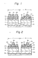
- Figure 1 illustrates a compound semiconductor IC device which has an n-p-n type heterojunction bipolar transistorin an area B and a MESFET in an area F.
- reference numeral 12 denotes an n-type Al x Ga 1-x As layer, 13 a p-type GaAs layer, 14 an n-type GaAs layer, and 16 to 20 electrodes.
- the layers 12 to 14 in the area B constitute the emitter, base and collector regions, respectively, of a bipolar transistor with a heterojunction between the emitter and base regions and the layer 14 in the area F constitutes a channel region of a MESFET.
- a bipolar transistor is preferably an n-p-n type so that the major carriers of the bipolar transistor are the electrons.
- the layer 14 should preferably be a collector region and the layer 12 an emitter region since, if the layer 12 were a collector region, the collector capacitance would be increased due to the longer horizontal length of the layer 12 over the layer 14, decreasing the switching speed of the device. Therefore, a heterojunction should be formed between the layers 12 and 13, i.e., the emitter and base regions.
- the forbidden energy band gap of Al x Ga 1 - x ⁇ s is wider than that of GaAs.
- the layers 12 and 13 are made of AIGaAs and GaAs respectively.
- a channel region of an FET preferably is made of an n-type layer so that the carrier is the electron.
- GaAs is preferred to Al x Ga 1 - x As for making a channel region since the mobility of the electron in AIGaAs is relatively small but that in GaAs is large. Therefore, a channel region of an FET is preferably constituted by an n-type GaAs layer. To attain this, the n-type layer 14 should be made of GaAs.
- the bipolar transistor in Figure 1 is a single heterojunction type bipolar transistor.
- Element isolation i.e., isolation between a bipolar transistor and a MESFET
- Element isolation is effected by selective etching to make a groove passing through the layers 14 to 11 and reaching the substrate 10 and to form mesa-shaped regions of the layers 11 to 14 in the areas B and F respectively.
- element isolation may be effected by implantation of O + , B + or H + ions.
- the collector, base, and emitter regions 14, 13 and 12 are also shaped by selective etching.
- Any electrode may be made by a conventional procedure.
- an emitter electrode 16, a collector electrode 18 and source and drain electrodes 20, which should be in ohmic contact with the n-type AIGaAs or GaAs layer 12 or 14, are made by forming gold-germanium/gold (AuGe/ Au) layers onto the layer 12 and 14 and heating them at approximately 450°C for one minute for alloying.
- a base electrode 17, which should be in ohmic contact with the p-type GaAs layer 13, is made by forming gold/zinc (Au/Zn) layers on the layer 13 and heating them at approximately 350°C for one minute for alloying.
- a gate electrode 19, which should be in Schottky contact with the n-type GaAs layer 14, is made by forming titanium/platinum/gold (Ti/Pt/Au) layers on the layer 14 in the area F. Wiring or interconnection between the elements may be carried out by any conventional procedure.
- an AIGaAs/GaAs IC device including a heterojunction bipolar transistor and a MESFET is obtained.
- Figure 2 illustrates a compound semiconductor IC device comprising a p-n-p type heterojunction bipolar transistor in an area B and a JFET in an area F.
- reference numeral 32 denotes a p-type Al x Ga 1-x As layer, 33 an n-type GaAs layer, 34 a p-type Al x Ga 1-x As layer, and 36 to 40 electrodes.
- the layers 32 to 34 in the area B constitute emitter, base, and collector regions, respectively, of a bipolar transistor with heterojunctions between the emitter and base regions and between the base and collector regions
- the layer 33 in the area F constitutes a channel region of a JFET with a pn junction made by the layers 33 and 34.
- n-p-n type is preferred for a compound semiconductor bipolar transistor
- a p-n-p type bipolar transistor is also possible, especially where the pn junction between the emitter and base regions is a step-type junction and the width of the base region is reduced.
- the device in Figure 2 does not necessarily have to have double heterojunctions. However, with double heterojunctions, the emitter and collector regions may optionally be used as collector and emitter regions, respectively.
- the n-type GaAs layer 33 is most preferable for the channel region of an FET.
- the p-type Al x Ga 1-x As layer 34 on the n-type GaAs layer 33 does not necessarily have to be removed, however, and the pn junction between the layers 33 and 34 may be used as a junction type gate of a JFET, which is preferable since a JFET may allow a wide range of gate voltage which can be varied. Further, if the p-type Al x Ga 1-x As layer 34 is left on the channel region, possible trouble in removing the layer 34 from channel region is eliminated. However, alternatively, a MESFET may be made.
- the fabrication of the device in Figure 2 is similar to that of the device in Figure 1. The differences are as follows: On a semi-insulating GaAs layer 30, an undoped GaAs buffer layer 31, a p-type Al 0.3 Ga 0.7 As layer 32 approximately 200 nm thick doped with Be in a concentration of approximately 2x 1 017 cm -3 , an n-type GaAs layer 33 approximately 50 nm thick doped with Si in a concentration of approximately 1 ⁇ 10 18 cm- 3 , and a p-type Al 0.3 Ga 0.7 As layer 34 approximately 200 nm thick doped with Be in a concentration of approximately 2 ⁇ 10 17 cm- 3 are continuously grown In selective etching of the p-type Al 0.3 Ga 0.7 As layer 34, shaping is effected not only in the area B for making the emitter or collector region but also in the area F for exposing the top surface of the n-type GaAs layer 33 on which source and drain electrodes 40 should be formed.
- a base electrode 37 and the source and drain electrodes 40 should be in ohmic contact with the n-type GaAs layer 33, and may be made of AuGe/Au layers.
- An emitter or collector electrode 36, a collector or emitter electrode 38, and a gate electrode 39 should be in ohmic contact with the p-type Al 0.3 Ga 0.7 As layer 32 or 34 and may be made of Au/Zn layers. There is no Schottky type electrode.
- the p-type Al 0.3 Ga 0.7 As layer 34 in the area F is non-selectively removed and a gate electrode of Ti/Pt/Au layers is made on the n-type GaAs layer.
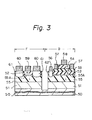
- Figure 3 illustrates a compound semiconductor IC device including a heterojunction bipolar transistor and a heterojunction FET.
- reference numeral 51 denotes an undoped GaAs buffer layer
- 52 an n-type Al x Ga 1-x As layer
- 53 a p-type GaAs layer
- 54 an n-type GaAs layer
- 55 an undoped GaAs layer
- 56 to 60 electrodes the heterojunction bipolar transistor in the area B is similar to that in Figure 1.
- the gate channel is a two- dimensional electron gas 55A formed by electrons- transmitted from the n-type Al x Ga 1-x As layer 52 to the undoped GaAs layer 55 owing to the larger electron affinity of the GaAs larger than the AIGaAs.
- a two-dimensional electron gas has increased electron mobility since it exists in a semiconductor layer without doped impurities, a cause of scattering of electrons.
- the electron mobility of such a two-dimensional electron gas of a heterojunction FET may be made further higher by cooling the FET to depress the lattice vibration of the semiconductor layer where the electrons move.
- the two-dimensional electron gas is also formed in the area B, enabling decreased emitter resistance.
- An undoped GaAs layer 55 approximately 300 nm is inserted between an undoped GaAs buffer layer 51 and an n-type Al x Ga 1-x As layer 52.
- An n-type GaAs layer 54 and a p-type GaAs layer 53 in the area F are removed, and electrodes 59 and 60 are formed on the n-type Al 0.3 Ga 0.7 As layer 52 in the area F.
- Reference numeral 50 denotes a semi-insulating GaAs substrate.
- the material and procedures of making the electrodes 56 to 60 may be the same as those for the electrodes 16 to 20 in Figure 1.
- the emitter electrode 56 and the source and drain electrodes 60 of AuGe/Au layers are heat-treated at approximately 450°C for one minute.
- the heat treatment allows alloying of the materials of the electrodes and the compound semi-conductor layer.
- the resultant alloy regions 61 and 62 may reach the undoped GaAs layer 55 through the n-type AI O . 3 Ga O . 7 As layer. These alloy regions 61 and 62 allow ohmic contact between the electrodes 60 and 56 and the two dimensional electron gas 55A.
- the above embodiments are only preferred examples within the overall possibilities of the present invention.
- the combination of the Al x Ga 1 - x As/GaAs may be replaced by: or other appropriate combinations of compound semi-conductors.
- the buffer layer may be a superlattice layer.
- a device including a heterojunction bipolar transistor and an FET, and embodying the present invention may be particularly useful in some cases.
- - FET's are suitable for memory cells because of their low power consumption and high switching speed, but the output drive capability of FET's may be inconveniently low, so that the speed of transporting information from the memory cell to a CPU, for example, is unduly restricted. It can therefore be particularly useful to include bipolar transistors, having high driving capability, as output buffers in a memory device employing FET's as memory cells.
- FET's can be effectively used to form current sources, which can permit satisfactory operation at lower supply voltages.
Landscapes
- Junction Field-Effect Transistors (AREA)
- Bipolar Transistors (AREA)
- Bipolar Integrated Circuits (AREA)
Claims (19)
caractérisé par une première couche (12,32) de matériau semiconducteur composé, d'un premier type (n, p) de conductivité, formée sur lesdites première et deuxième aires du substrat, par une deuxième couche (13, 33) de matériau semiconducteur composé, du type opposé (p, n) de conductivité, formée sur ladite première couche, et par un troisième couche (14, 34) de matériau semiconducteur composé, dudit premier type de conductivité (n, p), formée sur ladite deuxième couche, le matériau de l'une (12, 32) considérée, desdites première et troisième couches ayant une bande interdite d'énergie plus large que celle du matériau de ladite deuxième couche (13, 33); et
caractérisé en outre en ce que ledit transistor bipolaire est un transistor bipolaire à hétérojonc- tion possédant une région e base formée par une partie de ladite deuxième couche (13, 33), possédant une région d'émetteur formée par une partie de ladite couche considérée (12, 32) desdites première et troisième couches, et possédant une région de collecteur formée par l'autre (14, 34) desdites première et troisième couches, et en ce qu'une partie supplémentaire de l'une (14, 33) desdites première, deuxième et troisième couches constitue soit une région de canal du transistor à effet de champ, soit une région destinée à fournir des électrons à la région de canal de ce transistor.
Applications Claiming Priority (2)
| Application Number | Priority Date | Filing Date | Title |
|---|---|---|---|
| JP229431/83 | 1983-12-05 | ||
| JP58229431A JPH0626242B2 (ja) | 1983-12-05 | 1983-12-05 | 半導体集積回路装置 |
Publications (3)
| Publication Number | Publication Date |
|---|---|
| EP0144242A2 EP0144242A2 (fr) | 1985-06-12 |
| EP0144242A3 EP0144242A3 (en) | 1986-12-30 |
| EP0144242B1 true EP0144242B1 (fr) | 1990-04-18 |
Family
ID=16892117
Family Applications (1)
| Application Number | Title | Priority Date | Filing Date |
|---|---|---|---|
| EP84308457A Expired EP0144242B1 (fr) | 1983-12-05 | 1984-12-05 | Dispositif de circuit intégré à semi-conducteur composé |
Country Status (6)
| Country | Link |
|---|---|
| US (1) | US4821090A (fr) |
| EP (1) | EP0144242B1 (fr) |
| JP (1) | JPH0626242B2 (fr) |
| KR (1) | KR890003379B1 (fr) |
| CA (1) | CA1222330A (fr) |
| DE (1) | DE3482014D1 (fr) |
Families Citing this family (38)
| Publication number | Priority date | Publication date | Assignee | Title |
|---|---|---|---|---|
| WO1987000692A1 (fr) * | 1985-07-26 | 1987-01-29 | Hitachi, Ltd. | Dispositif a semi-conducteurs |
| DE3620686C2 (de) * | 1986-06-20 | 1999-07-22 | Daimler Chrysler Ag | Strukturierter Halbleiterkörper |
| JPS6312177A (ja) * | 1986-07-03 | 1988-01-19 | Fujitsu Ltd | 超高周波トランジスタ |
| US5162877A (en) * | 1987-01-27 | 1992-11-10 | Fujitsu Limited | Semiconductor integrated circuit device and method of producing same |
| EP0276981B1 (fr) * | 1987-01-27 | 1993-12-01 | Fujitsu Limited | Circuit intégré à semi-conducteur et procédé pour sa fabrication |
| JP2633848B2 (ja) * | 1987-03-25 | 1997-07-23 | 株式会社日立製作所 | 半導体装置 |
| JP2564296B2 (ja) * | 1987-03-25 | 1996-12-18 | 株式会社日立製作所 | 半導体装置 |
| DE3830102A1 (de) * | 1987-09-16 | 1989-03-30 | Licentia Gmbh | Si/sige-halbleiterkoerper |
| JP2675039B2 (ja) * | 1988-02-03 | 1997-11-12 | 株式会社日立製作所 | 半導体装置 |
| US5138408A (en) * | 1988-04-15 | 1992-08-11 | Nec Corporation | Resonant tunneling hot carrier transistor |
| US5012318A (en) * | 1988-09-05 | 1991-04-30 | Nec Corporation | Hybrid semiconductor device implemented by combination of heterojunction bipolar transistor and field effect transistor |
| JP2687519B2 (ja) * | 1988-12-06 | 1997-12-08 | 日本電気株式会社 | 半導体装置及びその製造方法 |
| US5068756A (en) * | 1989-02-16 | 1991-11-26 | Texas Instruments Incorporated | Integrated circuit composed of group III-V compound field effect and bipolar semiconductors |
| US5097312A (en) * | 1989-02-16 | 1992-03-17 | Texas Instruments Incorporated | Heterojunction bipolar transistor and integration of same with field effect device |
| EP0405214A3 (en) * | 1989-06-27 | 1991-06-05 | Siemens Aktiengesellschaft | Pin-fet combination with buried p-type layer |
| JPH0824162B2 (ja) * | 1989-07-10 | 1996-03-06 | 日本電装株式会社 | 半導体装置およびその製造方法 |
| JPH0368166A (ja) * | 1989-08-05 | 1991-03-25 | Matsushita Electric Ind Co Ltd | 化合物半導体装置 |
| US5276340A (en) * | 1989-11-21 | 1994-01-04 | Fujitsu Limited | Semiconductor integrated circuit having a reduced side gate effect |
| US5068705A (en) * | 1990-07-31 | 1991-11-26 | Texas Instruments Incorporated | Junction field effect transistor with bipolar device and method |
| US5077231A (en) * | 1991-03-15 | 1991-12-31 | Texas Instruments Incorporated | Method to integrate HBTs and FETs |
| US5166083A (en) * | 1991-03-28 | 1992-11-24 | Texas Instruments Incorporated | Method of integrating heterojunction bipolar transistors with heterojunction FETs and PIN diodes |
| JP3087370B2 (ja) * | 1991-09-10 | 2000-09-11 | 株式会社日立製作所 | 高速論理回路 |
| US5192698A (en) * | 1992-03-17 | 1993-03-09 | The United State Of America As Represented By The Secretary Of The Air Force | Making staggered complementary heterostructure FET |
| JPH06163829A (ja) * | 1992-07-31 | 1994-06-10 | Texas Instr Inc <Ti> | 集積回路とその製法 |
| JP3323544B2 (ja) * | 1992-08-21 | 2002-09-09 | 株式会社日立製作所 | 半導体装置 |
| US5250826A (en) * | 1992-09-23 | 1993-10-05 | Rockwell International Corporation | Planar HBT-FET Device |
| JPH1041400A (ja) * | 1996-07-26 | 1998-02-13 | Sony Corp | 半導体装置およびその製造方法 |
| US6043519A (en) * | 1996-09-12 | 2000-03-28 | Hughes Electronics Corporation | Junction high electron mobility transistor-heterojunction bipolar transistor (JHEMT-HBT) monolithic microwave integrated circuit (MMIC) and single growth method of fabrication |
| JP2003007976A (ja) * | 2001-06-25 | 2003-01-10 | Mitsubishi Electric Corp | 半導体装置及びモジュール装置 |
| US7015519B2 (en) * | 2004-02-20 | 2006-03-21 | Anadigics, Inc. | Structures and methods for fabricating vertically integrated HBT/FET device |
| DE102004037252A1 (de) * | 2004-07-31 | 2006-03-23 | Atmel Germany Gmbh | Verfahren zur Integration von drei Bipolartransistoren in einem Halbleiterkörper, Mehrschichtbauelement und Halbleiteranordnung |
| US20080026545A1 (en) * | 2006-07-28 | 2008-01-31 | Paul Cooke | Integrated devices on a common compound semiconductor III-V wafer |
| JP5056127B2 (ja) | 2007-04-05 | 2012-10-24 | セイコーエプソン株式会社 | メディア搬送機構及びそれを備えたメディア処理装置 |
| JP4524298B2 (ja) * | 2007-06-04 | 2010-08-11 | パナソニック株式会社 | 半導体装置の製造方法 |
| EP2180517A1 (fr) * | 2008-10-24 | 2010-04-28 | Epcos Ag | Transistor bipolaire pnp avec un collecteur latéral et procédé de fabrication |
| KR101649004B1 (ko) * | 2009-05-26 | 2016-08-17 | 스미또모 가가꾸 가부시키가이샤 | 반도체 기판, 반도체 기판의 제조 방법 및 전자 디바이스 |
| WO2011066862A1 (fr) * | 2009-12-03 | 2011-06-09 | Epcos Ag | Transistor bipolaire avec émetteur et collecteur latéraux, et procédé de fabrication |
| CN110943046A (zh) * | 2019-12-03 | 2020-03-31 | 李珂 | 一种双极性晶体管和场效应晶体管的整合结构及其制备方法 |
Family Cites Families (12)
| Publication number | Priority date | Publication date | Assignee | Title |
|---|---|---|---|---|
| US4063271A (en) * | 1972-07-26 | 1977-12-13 | Texas Instruments Incorporated | FET and bipolar device and circuit process with maximum junction control |
| JPS5718348B2 (fr) * | 1974-06-07 | 1982-04-16 | ||
| US4163237A (en) * | 1978-04-24 | 1979-07-31 | Bell Telephone Laboratories, Incorporated | High mobility multilayered heterojunction devices employing modulated doping |
| EP0033037B1 (fr) * | 1979-12-28 | 1990-03-21 | Fujitsu Limited | Dispositifs semiconducteurs à hétérojonction |
| JPS5727176U (fr) * | 1980-05-31 | 1982-02-12 | ||
| US4380774A (en) * | 1980-12-19 | 1983-04-19 | The United States Of America As Represented By The Secretary Of The Navy | High-performance bipolar microwave transistor |
| JPS5891681A (ja) * | 1981-11-27 | 1983-05-31 | Oki Electric Ind Co Ltd | 電界効果型トランジスタ |
| US4590502A (en) * | 1983-03-07 | 1986-05-20 | University Of Illinois | Camel gate field effect transistor device |
| US4593305A (en) * | 1983-05-17 | 1986-06-03 | Kabushiki Kaisha Toshiba | Heterostructure bipolar transistor |
| EP0162541A1 (fr) * | 1984-03-28 | 1985-11-27 | International Standard Electric Corporation | Transistor à effet de champ et photodiode intégrés à héterojonction |
| US4586071A (en) * | 1984-05-11 | 1986-04-29 | International Business Machines Corporation | Heterostructure bipolar transistor |
| US4593457A (en) * | 1984-12-17 | 1986-06-10 | Motorola, Inc. | Method for making gallium arsenide NPN transistor with self-aligned base enhancement to emitter region and metal contact |
-
1983
- 1983-12-05 JP JP58229431A patent/JPH0626242B2/ja not_active Expired - Lifetime
-
1984
- 1984-12-04 CA CA000469309A patent/CA1222330A/fr not_active Expired
- 1984-12-05 KR KR1019840007656A patent/KR890003379B1/ko not_active Expired
- 1984-12-05 DE DE8484308457T patent/DE3482014D1/de not_active Expired - Lifetime
- 1984-12-05 EP EP84308457A patent/EP0144242B1/fr not_active Expired
-
1987
- 1987-03-30 US US07/031,228 patent/US4821090A/en not_active Expired - Lifetime
Also Published As
| Publication number | Publication date |
|---|---|
| KR850005154A (ko) | 1985-08-21 |
| JPH0626242B2 (ja) | 1994-04-06 |
| JPS60120551A (ja) | 1985-06-28 |
| KR890003379B1 (ko) | 1989-09-19 |
| EP0144242A3 (en) | 1986-12-30 |
| US4821090A (en) | 1989-04-11 |
| DE3482014D1 (de) | 1990-05-23 |
| CA1222330A (fr) | 1987-05-26 |
| EP0144242A2 (fr) | 1985-06-12 |
Similar Documents
| Publication | Publication Date | Title |
|---|---|---|
| EP0144242B1 (fr) | Dispositif de circuit intégré à semi-conducteur composé | |
| US5479033A (en) | Complementary junction heterostructure field-effect transistor | |
| US4583105A (en) | Double heterojunction FET with ohmic semiconductor gate and controllable low threshold voltage | |
| US5012318A (en) | Hybrid semiconductor device implemented by combination of heterojunction bipolar transistor and field effect transistor | |
| EP0165798B1 (fr) | Dispositif semi-conducteur comprenant des transistors à canal N et à canal P et méthode de production | |
| JPH0714845A (ja) | Iii−v族材料系のハイブリッドバイポーラ・電界効果電力トランジスタ | |
| US4791072A (en) | Method for making a complementary device containing MODFET | |
| KR920010671B1 (ko) | 반도체장치 | |
| EP0200933A1 (fr) | Transistor à hétérojonction ayant des caractéristiques bipolaires | |
| JPH05315366A (ja) | 半導体装置 | |
| JPS61147577A (ja) | 相補型半導体装置 | |
| EP0092645A2 (fr) | Transistor et circuit comportant un transistor | |
| JPS6052060A (ja) | 電界効果トランジスタ | |
| US4811070A (en) | Heterojunction bipolar transistor with inversion layer base | |
| JP2530806B2 (ja) | 相補型論理構造 | |
| JP2643890B2 (ja) | トンネルトランジスタ | |
| JPH02111073A (ja) | 絶縁ゲート電界効果トランジスタおよびその集積回路装置 | |
| JP2655594B2 (ja) | 集積型半導体装置 | |
| JPH0763051B2 (ja) | 半導体装置 | |
| JPS59222964A (ja) | 半導体装置 | |
| JP2834172B2 (ja) | 電界効果トランジスタ | |
| JP3006792B2 (ja) | ヘテロ構造電界効果トランジスタ | |
| JPS61296754A (ja) | 半導体装置とその製造方法 | |
| JPH0154868B2 (fr) | ||
| JPH0797633B2 (ja) | 電界効果トランジスタ |
Legal Events
| Date | Code | Title | Description |
|---|---|---|---|
| PUAI | Public reference made under article 153(3) epc to a published international application that has entered the european phase |
Free format text: ORIGINAL CODE: 0009012 |
|
| AK | Designated contracting states |
Designated state(s): DE FR GB IT |
|
| PUAL | Search report despatched |
Free format text: ORIGINAL CODE: 0009013 |
|
| AK | Designated contracting states |
Kind code of ref document: A3 Designated state(s): DE FR GB IT |
|
| 17P | Request for examination filed |
Effective date: 19870206 |
|
| 17Q | First examination report despatched |
Effective date: 19880930 |
|
| ITF | It: translation for a ep patent filed | ||
| GRAA | (expected) grant |
Free format text: ORIGINAL CODE: 0009210 |
|
| AK | Designated contracting states |
Kind code of ref document: B1 Designated state(s): DE FR GB IT |
|
| REF | Corresponds to: |
Ref document number: 3482014 Country of ref document: DE Date of ref document: 19900523 |
|
| ET | Fr: translation filed | ||
| PLBE | No opposition filed within time limit |
Free format text: ORIGINAL CODE: 0009261 |
|
| STAA | Information on the status of an ep patent application or granted ep patent |
Free format text: STATUS: NO OPPOSITION FILED WITHIN TIME LIMIT |
|
| 26N | No opposition filed | ||
| ITTA | It: last paid annual fee | ||
| REG | Reference to a national code |
Ref country code: GB Ref legal event code: IF02 |
|
| PGFP | Annual fee paid to national office [announced via postgrant information from national office to epo] |
Ref country code: GB Payment date: 20031203 Year of fee payment: 20 |
|
| PGFP | Annual fee paid to national office [announced via postgrant information from national office to epo] |
Ref country code: FR Payment date: 20031210 Year of fee payment: 20 |
|
| PGFP | Annual fee paid to national office [announced via postgrant information from national office to epo] |
Ref country code: DE Payment date: 20031218 Year of fee payment: 20 |
|
| PG25 | Lapsed in a contracting state [announced via postgrant information from national office to epo] |
Ref country code: GB Free format text: LAPSE BECAUSE OF EXPIRATION OF PROTECTION Effective date: 20041204 |
|
| REG | Reference to a national code |
Ref country code: GB Ref legal event code: PE20 |