EP0175437A1 - Herstellung von GaAs-HEMT's des Anreicherungs- und Verarmungstyps - Google Patents
Herstellung von GaAs-HEMT's des Anreicherungs- und Verarmungstyps Download PDFInfo
- Publication number
- EP0175437A1 EP0175437A1 EP85303057A EP85303057A EP0175437A1 EP 0175437 A1 EP0175437 A1 EP 0175437A1 EP 85303057 A EP85303057 A EP 85303057A EP 85303057 A EP85303057 A EP 85303057A EP 0175437 A1 EP0175437 A1 EP 0175437A1
- Authority
- EP
- European Patent Office
- Prior art keywords
- layer
- etching
- semiconductor
- mode
- semiconductor layer
- Prior art date
- Legal status (The legal status is an assumption and is not a legal conclusion. Google has not performed a legal analysis and makes no representation as to the accuracy of the status listed.)
- Granted
Links
Images


Classifications
-
- H—ELECTRICITY
- H10—SEMICONDUCTOR DEVICES; ELECTRIC SOLID-STATE DEVICES NOT OTHERWISE PROVIDED FOR
- H10D—INORGANIC ELECTRIC SEMICONDUCTOR DEVICES
- H10D30/00—Field-effect transistors [FET]
- H10D30/40—FETs having zero-dimensional [0D], one-dimensional [1D] or two-dimensional [2D] charge carrier gas channels
- H10D30/47—FETs having zero-dimensional [0D], one-dimensional [1D] or two-dimensional [2D] charge carrier gas channels having two-dimensional [2D] charge carrier gas channels, e.g. nanoribbon FETs or high electron mobility transistors [HEMT]
- H10D30/471—High electron mobility transistors [HEMT] or high hole mobility transistors [HHMT]
- H10D30/475—High electron mobility transistors [HEMT] or high hole mobility transistors [HHMT] having wider bandgap layer formed on top of lower bandgap active layer, e.g. undoped barrier HEMTs such as i-AlGaN/GaN HEMTs
- H10D30/4755—High electron mobility transistors [HEMT] or high hole mobility transistors [HHMT] having wider bandgap layer formed on top of lower bandgap active layer, e.g. undoped barrier HEMTs such as i-AlGaN/GaN HEMTs having wide bandgap charge-carrier supplying layers, e.g. modulation doped HEMTs such as n-AlGaAs/GaAs HEMTs
-
- H—ELECTRICITY
- H10—SEMICONDUCTOR DEVICES; ELECTRIC SOLID-STATE DEVICES NOT OTHERWISE PROVIDED FOR
- H10P—GENERIC PROCESSES OR APPARATUS FOR THE MANUFACTURE OR TREATMENT OF DEVICES COVERED BY CLASS H10
- H10P50/00—Etching of wafers, substrates or parts of devices
- H10P50/20—Dry etching; Plasma etching; Reactive-ion etching
- H10P50/24—Dry etching; Plasma etching; Reactive-ion etching of semiconductor materials
- H10P50/246—Dry etching; Plasma etching; Reactive-ion etching of semiconductor materials of Group III-V materials
-
- H—ELECTRICITY
- H10—SEMICONDUCTOR DEVICES; ELECTRIC SOLID-STATE DEVICES NOT OTHERWISE PROVIDED FOR
- H10D—INORGANIC ELECTRIC SEMICONDUCTOR DEVICES
- H10D84/00—Integrated devices formed in or on semiconductor substrates that comprise only semiconducting layers, e.g. on Si wafers or on GaAs-on-Si wafers
- H10D84/01—Manufacture or treatment
- H10D84/0123—Integrating together multiple components covered by H10D12/00 or H10D30/00, e.g. integrating multiple IGBTs
- H10D84/0126—Integrating together multiple components covered by H10D12/00 or H10D30/00, e.g. integrating multiple IGBTs the components including insulated gates, e.g. IGFETs
- H10D84/0163—Integrating together multiple components covered by H10D12/00 or H10D30/00, e.g. integrating multiple IGBTs the components including insulated gates, e.g. IGFETs the components including enhancement-mode IGFETs and depletion-mode IGFETs
-
- H—ELECTRICITY
- H10—SEMICONDUCTOR DEVICES; ELECTRIC SOLID-STATE DEVICES NOT OTHERWISE PROVIDED FOR
- H10D—INORGANIC ELECTRIC SEMICONDUCTOR DEVICES
- H10D84/00—Integrated devices formed in or on semiconductor substrates that comprise only semiconducting layers, e.g. on Si wafers or on GaAs-on-Si wafers
- H10D84/01—Manufacture or treatment
- H10D84/02—Manufacture or treatment characterised by using material-based technologies
- H10D84/05—Manufacture or treatment characterised by using material-based technologies using Group III-V technology
-
- H—ELECTRICITY
- H10—SEMICONDUCTOR DEVICES; ELECTRIC SOLID-STATE DEVICES NOT OTHERWISE PROVIDED FOR
- H10P—GENERIC PROCESSES OR APPARATUS FOR THE MANUFACTURE OR TREATMENT OF DEVICES COVERED BY CLASS H10
- H10P50/00—Etching of wafers, substrates or parts of devices
- H10P50/20—Dry etching; Plasma etching; Reactive-ion etching
- H10P50/24—Dry etching; Plasma etching; Reactive-ion etching of semiconductor materials
- H10P50/242—Dry etching; Plasma etching; Reactive-ion etching of semiconductor materials of Group IV materials
-
- H—ELECTRICITY
- H10—SEMICONDUCTOR DEVICES; ELECTRIC SOLID-STATE DEVICES NOT OTHERWISE PROVIDED FOR
- H10D—INORGANIC ELECTRIC SEMICONDUCTOR DEVICES
- H10D84/00—Integrated devices formed in or on semiconductor substrates that comprise only semiconducting layers, e.g. on Si wafers or on GaAs-on-Si wafers
- H10D84/01—Manufacture or treatment
- H10D84/02—Manufacture or treatment characterised by using material-based technologies
- H10D84/03—Manufacture or treatment characterised by using material-based technologies using Group IV technology, e.g. silicon technology or silicon-carbide [SiC] technology
- H10D84/038—Manufacture or treatment characterised by using material-based technologies using Group IV technology, e.g. silicon technology or silicon-carbide [SiC] technology using silicon technology, e.g. SiGe
-
- Y—GENERAL TAGGING OF NEW TECHNOLOGICAL DEVELOPMENTS; GENERAL TAGGING OF CROSS-SECTIONAL TECHNOLOGIES SPANNING OVER SEVERAL SECTIONS OF THE IPC; TECHNICAL SUBJECTS COVERED BY FORMER USPC CROSS-REFERENCE ART COLLECTIONS [XRACs] AND DIGESTS
- Y10—TECHNICAL SUBJECTS COVERED BY FORMER USPC
- Y10S—TECHNICAL SUBJECTS COVERED BY FORMER USPC CROSS-REFERENCE ART COLLECTIONS [XRACs] AND DIGESTS
- Y10S438/00—Semiconductor device manufacturing: process
- Y10S438/97—Specified etch stop material
Definitions
- the present invention relates to a semiconductor device comprising an enhancement-mode (E-mode) field-effect transistor (FET) and a depletion-mode (D-mode) FET which are operated at a high speed by using a two-dimensional electron gas.
- E-mode enhancement-mode
- D-mode depletion-mode
- the above FET's comprise a semi-insulating gallium-arsenide (GaAs) substrate, an undoped GaAs channel layer, an N-type aluminium-gallium-arsenide (AlGaAs) electron-supply layer, and an N-type GaAs cap layer, which layers are successively formed on the substrate.
- a threshold voltage Vth of the FET depends on the thickness of a semiconductor layer including the N-type AlGaAs electron-supply layer between the undoped GaAs channel layer and a contacting bottom of a gate electrode.
- a logic circuit e.g., a basic inverter, comprises an enhancement/depletion (E/D) constitution consisting of an E-mode FET and a D-mode FET.
- E/D enhancement/depletion
- an E/D constitution semiconductor device for such a logic circuit it is necessary to form the E-mode FET having one threshold voltage and the D-mode FET having another threshold voltage in the same semiconductor substrate.
- the E/D constitution semiconductor device is formed by using FETs operating at a high speed by using two-dimensional electron gas, it is necessary to form the E-mode FET and D-mode FET on the same semi-insulating substrate in such manner that the D-mode FET has a thickness of a semiconductor layer between the undoped channel layer and the contacting bottom of the gate electrode thereof different from that of the E-mode FET.
- Such an E/D constitution semiconductor device has been produced by methods proposed, for example, in EP-A-0119089 and EP-A-0143656.
- the proposed methods utilize the additional formation of one or two thin AlGaAs layers and the adoption of a reactive ion etching (RI E) method using an etchant gas comprising CC1 2 F 2 , which will etch GaAs very rapidly as compared with AlGaAs.
- RI E reactive ion etching
- the etching rate for GaAs is about 200 times faster than that for AlGaAs.
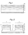
- an E-mode FET region of a contact (cap) GaAs layer, an one etching stoppable AlGaAs layer, and a GaAs layer on an AlGaAs electron-supply layer are selectively etched by a wet chemical etching method to form a recess, as shown in Figure 10.
- a portion of the AlGaAs electron-supply layer may be etched in some of the recesses among all of the recesses in a wafer.
- EP-A-0143656 after at least a contact (cap) GaAs layer and an (second) etching stoppable AlGaAs layer are selectively etched in an E-mode FET to form a recess, a reactive ion etching treatment using CC1 2 F 2 gas is performed so as to simultaneously complete grooves for gate electrodes of the E-mode and D-mode FET's.
- a reactive ion etching treatment using CC1 2 F 2 gas is performed so as to simultaneously complete grooves for gate electrodes of the E-mode and D-mode FET's.
- the etching step at least the above-mentioned AlGaAs layer in the E-mode FET region is etched.
- the etch rate for AlGaAs is, in practice, varied, and in the second embodiment, another (first) etching stoppable AlGaAs layer in GaAs layer between the former AlGaAs layer and the electron-supply layer and both the AlGaAs layers should be made to have the exactly same thickness.
- Such factors cause about variations in the thickness of a semiconductor layer between the undoped GaAs layer and the contacting bottom of the gate electrodes, namely, variations in the threshold voltages of the E-mode and D-mode FETs.
- the proposed producing methods cannot sufficiently attain an exact control of the groove depth for gate electrodes by etching, namely, uniformity of the threshold voltages of the E-mode and D-mode FETs formed in a wafer is relatively low.
- a thickness variation is ⁇ 1 nm corresponding to three atom layers.
- a method of producing a semiconductor device which comprises an E-mode FET and a D-mode FET and utilizing a two-dimensional electron gas, comprises the steps of: (a) forming a first semiconductor layer of a channel layer, in which the two-dimensional electron gas is generated, on a semi-insulating semiconductor substrate; (b) forming a second semiconductor layer of an electron-supply layer; (c) forming a third semiconductor layer of an adjusting layer for the threshold voltage of the D-mode transistor; (d) forming a fourth semiconductor layer of a first etching-stoppable layer; (e) forming a fifth semiconductor layer of an ohmic-contactable layer, the first to fifth layers being deposited successively on the substrate by a molecular beam epitaxy (MBE) method or a metal organic chemical vapor deposition (MOCVD) method; (f) forming a sixth layer of a second etching-stoppable layer being of a semiconductor or insulating material on the fifth layer; (g)
- MBE
- the first etching treatment removes the portion of the fourth semiconductor layer in the E-mode FET region and the portion of the sixth layer in the D-mode FET region
- the second etching treatment using an etchant different from that used in the first etching treatment removes the portion of the third semiconductor layer in the E-mode FET region and the portion of the fifth semiconductor layer in the D-mode FET region.
- an undoped GaAs channel layer (a first semiconductor layer) 2, an N-type AlGaAs electron-supply layer (a second semiconductor layer) 3, an N-type GaAs threshold voltage controlling layer (a third semiconductor layer) 4, an N-type AlGaAs first stoppable layer (a fourth semiconductor layer) 5, an N-type GaAs ohmic-contactable layer (a fifth semiconductor layer) 6, an N-type AlGaAs second etching-stoppable layer (a sixth semiconductor layer) 7, and an N-type GaAs ohmic-contactable layer (a seventh semiconductor layer) 8 are formed (i.e., epitaxially grown) in sequence by an MBE method or an MOCVD method.
- the first undoped GaAs layer 2 has a thickness of from 50 nm to 1 ⁇ m. A two-dimensional electron gas is generated in the first layer 2 near a heterojunction interface between the first layer 2 and the second N-type AlGaAs layer 3.
- the second N-type AlGaAs layer 3 has a thickness of 18 to 60 nm, preferably 30 nm, and is doped with silicon (Si) impurities of a carrier (donor) concentration of from 1 x 10 17 to 5 x 10 18 cm -3 , preferably 2 x 10 18 cm - 3 .
- a threshold voltage of the E-mode FET substantially depends on the thickness of the second layer 3.
- the third N-type GaAs layer 4 has a thickness of 2 to 50 nm, preferably 10 nm, and is doped with Si impurities of a carrier concentration similar to that of the second layer 3.
- the fourth N-type AlGaAs layer 5 has a thickness of from 1.5 to 30 nm, preferably from 3 to 5 nm, and is doped with Si impurities of a carrier concentration similar to that of the second layer 3.
- a threshold voltage of the D-mode FET substantially depends on the total thickness of the second layer 3, third layer 4, and fourth layer 5. Therefore, a voltage difference between the threshold voltages of the E-mode and D-mode FET's depends on the thicknesses of the third layer 4 and fourth layer 5.
- the fifth N-type GaAs layer 6 has a thickness of from 40 to 200 nm, preferably 80 nm, and is doped with Si impurities of a carrier concentration similar to that of the second layer 3.
- the sixth N-type AlGaAs layer 7 has a thickness of from 1.5 to 30 nm, preferably from 3 to 5 nm, and is doped with Si impurities of a carrier concentration similar to that of the second layer 3. It is not necessary for the thickness of the sixth layer 6 of an etching-stoppable layer to coincide with that of the fourth layer 5.
- the seventh N-type GaAs layer 8 has a thickness of from 10 to 100 nm, preferably 30 nm, and is doped with Si impurities of a carrier concentration similar to that of the second layer 3. Since AlGaAs is easily oxidized to form an insulating layer of aluminum oxide which impedes electrical contact of the AlGaAs layer with an electrode, the seventh GaAs layer 8 should be formed as a cap layer.
- the semiconductor layers 8 to 2 and the semiconductor substrate 1 are selectively etched by a wet etching method using a suitable etchant, e.g., hydrofluoric acid (HF), to form a groove 9, an E-mode FET region "E” island, and a D-mode FET region "D” island.
- a suitable etchant e.g., hydrofluoric acid (HF)
- HF hydrofluoric acid
- This groove 9 extends into the substrate 1.
- an ion-implantation treatment can be adopted. In this case, oxygen ions or protons are doped into the portion corresponding to the groove 9 to form an insulating region.
- portions of the N-type GaAs layer 8 and the N-type AlGaAs layer 7 corresponding to a gate region of the E-mode FET are etched by a suitable etching method (e.g., a wet etching method using HF solution) to form a recess 10 in the E region.
- a suitable etching method e.g., a wet etching method using HF solution
- a portion of the N-type GaAs layer 6 is exposed and may be simultaneously etched.
- an insulating layer 11 being of, e.g., silicon dioxide (Si0 2 ), is formed over the whole of the exposed surface by a chemical vapor deposition (CVD) method.
- the SiO 2 layer 11 has a thickness of, e.g., about 300 nm.
- the insulating (Si0 2 ) layer 11 is coated with a resist layer (not shown) having openings and is then selectively etched by, e.g., a wet etching method using an HF solution, to form contact openings therein.
- a metal film of AuGe/Au, AuGe/Ni/Au, AuGe/Ni, or the like is formed on the resist layer and the exposed portions of the seventh N-type GaAs layer 7 in the openings by a vapor deposition method.
- the resist layer is then removed by a suitable solvent, whereby a portion of the metal film on the resist layer is also removed.
- electrode metal portions 12, 13, 14, and 15 remain on the seventh N-type GaAs layer 8.
- a heat treatment for alloying e.g., at about 450°C for 1 minute, is carried out to form ohmic-contact electrodes 12 to 15 of the source and drain electrodes of the E-mode and D-mode FET's.
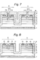
- a resist layer (a masking layer) 16 is coated, exposed, and developed to form openings 17E and 17D for the formation of grooves for gate electrodes of the E-mode and D-mode FET's, respectively.
- the SiO 2 layer 11 is etched through the openings 17E and 17D by, e.g., a wet etching method using an HF solution, so that openings 18E and 18D are formed in the Si0 2 layer 11.
- a selective dry etching treatment in this case a reactive ion etching (RIE) treatment using an etchant gas comprising CC1 2 F 2 , is performed so as to etch the fifth N-type GaAs layer 6 in the E region through the opening 17E and the seventh N-type GaAs layer 8 in the D region, to form openings 19E and 19D, respectively.
- RIE reactive ion etching
- the fourth N-type AlGaAs layer 5 in the E region and the sixth N-type AlGaAs layer 7 in the D region serve as etching-stoppable layers.
- the above-mentioned RIE method using CC1 2 F 2 gas can etch GaAs about 200 times faster than AlGaAs.
- the etching is automatically stopped at the surfaces of the N-type AlGaAs layers 5 and 7.
- the exposed portions of the AlGaAs layers 5 and 7 in the openings 17E to 19E and 17D to 19D are etched by, e.g., a wet etching method using an HF solution, to expose the third N-type GaAs layer 4 in the E region and the fifth N-type GaAs layer 6 in the D region. Since this etching treatment is performed for the purpose of removing a AlGaAs layer, and since the thickness of the AlGaAs layers 5 and 7 is thin, it is easy to control the etching of the AlGaAs layers 5 and 7 without the complete removal of the third and fifth GaAs layers 4 and 6.
- openings 20E and 20D are formed in the AlGaAs layers 5 and 7 and portions of the GaAs layer 4 and 6. It is possible to perform the etching treatment by a dry etching method using an etchant gas, e.g. Ar, He, H 2 , or BCl 3 instead of the wet etching methods. And also, it is possible to use a wet etching of a mixture of I 2 and KI which can etch AlGaAs about 30 ⁇ 40 times faster than GaAs.
- an etchant gas e.g. Ar, He, H 2 , or BCl 3
- a selective dry etching (in this case, RIE) treatment using CC1 2 F 2 gas is performed so as to etch the third GaAs layer 4 in the E region through the opening 17E and the fifth GaAs layer 6 in the D region through the opening 17D so that openings 21E and 21D are formed, respectively.
- the second N-type AlGaAs layer 3 in the E region and the fourth N-type AlGaAs layer 5 in the D region serve as etching-stoppable layers.
- grooves 22E and 22D consisting of the openings 18E to 21E and 18D to 21D, respectively, are completed. The point is that this etching treatment in Fig.
- etching process for each layers are performed step by step so as to controls the threshold voltage acurately.
- etching process of Fig. 7 another etching process can be possible, for example, a selective dry etching of reactive ion etching using a gas CC1F 2 , or selective wet etching H 2 0 2 + NH 4 0H.
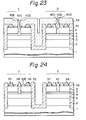
- a metal layer for Schottky barrier of, e.g., aluminum (Al), is formed by, e.g., a vapor deposition method, on the remaining resist layer 16 and in the grooves 22E and 22D.
- the thickness of the metal layer is, e.g., about 300 nm.
- the resist layer 16 is then removed by a suitable solvent, whereby a portion of the metal film on the resist layer 16 is also removed.
- metal portions i.e., gate electrodes 23 and 24 of the E-mode and D-mode FET's, respectively, are formed. Therefore, a semiconductor device comprising the E-mode and D-mode FET's is obtained.
- the threshold voltage of the E-mode FET depends on the thickness of the second AlGaAs electron-supply layer 3, and the threshold voltage of the D-mode FET depends on the total thickness of the second, third, and fourth semiconductor layers 3, 4 and 5.
- the AlGaAs layers 3 and 5 are not substantially etched in the production in accordance with the present invention, accordingly accurate threshold voltages are obtained and the variation of the threshold voltages in a wafer is slight.
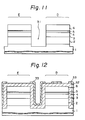
- a semiconductor device illustrated in Fig. 9 is obtained.
- the production steps are the same as those of the above-mentioned first embodiment except that in the formation step of the recess 10 in Fig. 3 the sixth and seventh semiconductor layers 7 and 8 in the E region are completely removed.
- the semiconductor substrate 1 and the semiconductor layers 2, 3, 4, 5 and 6 used in the first embodiment are utilized in this case.
- the semiconductor layers 6 to 2 and the substrate 1 are selectively etched by a wet etching method using an HF solution to form a groove 31 for isolating an E-mode FET region "E" island and a D-mode FET region "D" island.
- the groove 31 extends into the substrate 1. It is possible to adopt an ion-implantation treatment for forming an isolation region instead of the groove 31.
- an insulating layer 32 of, e.g., Si0 2 is formed over the whole of the exposed surface by a CVD method.
- the thickness of the insulating layers 32 and 33 are, e.g., about 300 nm and 100 nm, respectively.
- the another insulating Si 3 N 4 layer 33 is coated with a resist layer (not shown) and is etched by, e.g., a dry etching method using an etchant gas comprising CF 4 gas, to form an opening corresponding to the E region and openings corresponding to source and drain electrodes of the D-mode FET.
- a dry etching method using an etchant gas comprising CF 4 gas, to form an opening corresponding to the E region and openings corresponding to source and drain electrodes of the D-mode FET.
- Another resist layer (not shown) having openings corresponding to the source and drain electrodes of the E-mode and D-mode FET's is formed on the exposed surface and then the insulating Si0 2 layer 32 is selectively etched by, e.g., a wet etching method using an HF solution, to form contact openings therein. Leaving the resist layer, a metal film of AuGe/Au or the like is formed on the resist layer and on the exposed portions of the fifth N-type GaAs layer 5 in the contact openings by a vapor deposition method. The resist layer is then removed by a suitable solvent, whereby a portion of the metal film on the resist layer is also removed.
- electrode metal portions 35, 36, 37, and 38 remain on the fifth GaAs layer 5, as illustrated in Fig. 13.
- a heat treatment for alloying is carried out to form ohmic-contact electrodes 35 to 38 of the source and drain electrodes of the E-mode and D-mode FET's.
- a resist layer 39 is applied, exposed and developed to form openings 40E and 40D corresponding to gate electrodes of the FETs.
- openings 40E and 40D corresponding to gate electrodes of the FETs.
- a portion of the insulating layer 32 is exposed and in the opening 40D a portion of the other insulating layer 33 is exposed.
- the insulating Si0 2 layer 32 is etched through the opening 40E by, e.g., a wet etching method using an HF solution, to form an opening 41E therein.
- the fifth GeAs layer 6 is etched through the openings 40E and 41E by a selective etching treatment (i.e., an RIE treatment) using CC1 2 p 2 gas to form an opening 40E in which the fourth N-type AlGaAs layer 5 is exposed in the E region.
- the fourth AlGaAs layer 5 serves as an etching-stoppable layer.
- the other insulating Si 3 N 4 layer 33 in the D region serves as an etching-stoppable layer.
- the exposed portion of the insulating Si3N 4 layer 33 in the D region is etched by a wet etching method using a phosphoric acid (H 3 P0 4 ) solution to expose the insulating layer 32, and then the exposed portion of the fourth AlGaAs layer 5 in the opening 40E and the insulating layer 32 in the D region are simultaneously etched by a wet etching method using an HF solution to form openings 43E and 43D, respectively.
- a portion of the third N-type GaAs layer 4 is exposed and in the opening 43D a portion of the fifth GaAs layer 6 is exposed.
- the fourth AlGaAs layer 5 is thin, it is easy to control the etching of the AlGaAs layer without the complete removal of the third GaAs layer 4. It is possible to perform the etching treatment by a dry etching method instead of the wet etching method.
- a selective dry etching (in this case, RIE) treatment using CC1 2 F 2 gas is performed to etch the third GaAs layer 4 through the opening 40E and the fifth GaAs layer 6 through the opening 40D, so that openings 44E and 44D are formed, respectively.
- the second N-type AlGaAs layer 3 in the E region and the fourth N-type AlGaAs layer 5 in the D region serve as etching-stoppable layers.
- grooves 45E and 45D consisting of the openings 41E, 42E, 43E, and 44E, and 43D and 44D, respectively, are completed.
- a metal layer for a Schottky barrier e.g., of Al
- the thickness of the Al layer is, e.g., about 300 nm.
- the resist layer 39 is then removed by a suitable solvent, whereby a portion of the metal layer on the resist layer 39 is also removed.
- metal portions i.e., gate electrodes 46 and 47 of the E-mode and D-mode FET's, are formed. Therefore, a semiconductor device comprising E-mode and D-mode FET's is obtained.
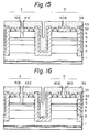
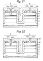
- FIG. 19 through 24 a method of producing an E/D constitution semiconductor device in accordance with a fourth embodiment of the present invention is now explained.
- the production steps of the fourth embodiment are similar to those of the third embodiment.
- the same reference numerals used in the fourth embodiment as those used in the third embodiment indicate the same elements.
- the insulating (e.g., Si0 2 ) layer 32 is formed over the whole of the exposed surface including the groove 31, as shown in Fig. 12, a resist layer 51 with an opening 52E is formed on the insulating Si0 2 layer 32, as illustrated in Fig. 19. Then the insulating SiO 2 layer 32 is etched by a wet etching method using an HF solution to decrease the thickness thereof (e.g., about 300 nm). The decreased insulating portion 32E in the E region has a thickness of, e.g., about 200 nm.
- the resist layer 51 is removed and another resist layer (not shown) is then formed on the insulating layer 32 including the decreased portion 32E.
- This other resist layer has openings corresponding to source and drain electrodes of the FET's.
- the insulating layer is selectively etched by a wet etching method using an HF solution to form contact openings therein.
- a metal layer of AuGe/Au or the like is deposited on the resist layer and in the contact openings and then the resist layer, together with a portion of the metal layer thereon, is removed. As a result, the source and drain electrodes 35, 36, 37, and 38 are formed.
- the resist layer 39 having the openings 40D and 40E is formed on the insulating layer 32 and the electrodes 35 to 38.
- a wet etching treatment using an HF solution is performed to etch the decreased insulating Si0 2 portion 32E through the opening 40E to form an opening 53E.
- the insulating layer 32 in the D region is also etched to form a recess 53D.
- a selective dry etching (i.e., RIE) treatment using CC1 2 F 2 gas is performed to etch the fifth N-type GaAs layer 6 through the opening 40E.
- the opening 42E is formed in the fifth GaAs layer 6, and a portion of the fourth AlGaAs layer 4 is exposed in the opening 42E.
- the fourth AlGaAs layer 4 and the insulating Si0 2 layer 32 serve as etching-stoppable layers.
- the exposed portion of the fourth AlGaAs layer 5 in the opening 40E and the insulating Sio 2 layer 32 in the opening 40D are etched by a wet etching method using an HF solution to form the openings 43E and 43D, respectively.
- a portion of the third N-type GaAs layer 4 is exposed in the opening 43E, and a portion of the fifth GaAs layer 6 is exposed in the opening 43D.
- a selective dry etching (in this case, RIE) treatment using CC1 2 F 2 gas is performed to etch the third GaAs layer 4 and the fifth GaAs layer 6.
- the second N-type AlGaAs layer 3 in the E region and the fourth N-type AlGaAs layer 5 in the D region serve as etching-stoppable layers.
- grooves 45E and 45D for gate electrodes of the E-mode and D-mode FETs are completed.
- germanium (Ge), indium-antimonide (InSb), or indium-arsenide (InAs) may be used for the first layer 2 and AlGaAs, GaAs, cadmium-telluride (CdTe), or gallium-antimonide (GaSb) may be used for the second layer 3.
- the layers 4 and 6 may be made of Ge, InSb, or InAs
- the layers 5 and 7 may be made of AlGaAs, CdTe, or GaSb. It is possible to adopt a suitable etchant in accordance with compound semiconductor materials used for a semiconductor device in the embodiments of the present invention.
Landscapes
- Junction Field-Effect Transistors (AREA)
Applications Claiming Priority (4)
| Application Number | Priority Date | Filing Date | Title |
|---|---|---|---|
| JP59086243A JPS60231368A (ja) | 1984-05-01 | 1984-05-01 | 半導体装置の製造方法 |
| JP86243/84 | 1984-05-01 | ||
| JP144367/84 | 1984-07-13 | ||
| JP14436784A JPS6124265A (ja) | 1984-07-13 | 1984-07-13 | 半導体装置の製造方法 |
Publications (2)
| Publication Number | Publication Date |
|---|---|
| EP0175437A1 true EP0175437A1 (de) | 1986-03-26 |
| EP0175437B1 EP0175437B1 (de) | 1988-11-30 |
Family
ID=26427400
Family Applications (1)
| Application Number | Title | Priority Date | Filing Date |
|---|---|---|---|
| EP85303057A Expired EP0175437B1 (de) | 1984-05-01 | 1985-04-30 | Herstellung von GaAs-HEMT's des Anreicherungs- und Verarmungstyps |
Country Status (4)
| Country | Link |
|---|---|
| US (1) | US4615102A (de) |
| EP (1) | EP0175437B1 (de) |
| KR (1) | KR890004456B1 (de) |
| DE (1) | DE3566594D1 (de) |
Cited By (7)
| Publication number | Priority date | Publication date | Assignee | Title |
|---|---|---|---|---|
| EP0371686A1 (de) * | 1988-11-29 | 1990-06-06 | Fujitsu Limited | Halbleiterbauteil und Verfahren zur dessen Herstellung |
| EP0367411A3 (de) * | 1988-10-12 | 1990-08-08 | Fujitsu Limited | Heteroübergang-Halbleiteranordnungen und Verfahren zu deren Herstellung |
| EP0368468A3 (en) * | 1988-10-08 | 1990-08-16 | Fujitsu Limited | Heterojunction semiconductor devices and methods of making the same |
| EP0378894A3 (de) * | 1988-12-28 | 1990-11-28 | AT&T Corp. | Herstellung von integrierten Schaltungen aus GaAs |
| EP0401537A3 (de) * | 1989-05-14 | 1991-02-27 | Texas Instruments Incorporated | Dynamische RAM-Zelle mit hoher Dichte |
| EP0287793A3 (de) * | 1987-04-23 | 1991-03-06 | International Business Machines Corporation | Substratprodukt für integrierte Schaltung |
| EP0397148A3 (de) * | 1989-05-10 | 1991-05-15 | Fujitsu Limited | Heterostrukturbauelement und dessen Herstellungsverfahren |
Families Citing this family (36)
| Publication number | Priority date | Publication date | Assignee | Title |
|---|---|---|---|---|
| US4916498A (en) * | 1985-09-15 | 1990-04-10 | Trw Inc. | High electron mobility power transistor |
| US4829022A (en) * | 1985-12-09 | 1989-05-09 | Nippon Telegraph And Telephone Corporation | Method for forming thin films of compound semiconductors by flow rate modulation epitaxy |
| FR2598256B1 (fr) * | 1986-04-30 | 1988-07-08 | Thomson Csf | Procede de gravure seche selective de couches de materiaux semi-conducteurs iii-v, et transistor obtenu par ce procede. |
| JPH04280436A (ja) * | 1990-09-28 | 1992-10-06 | Motorola Inc | 相補型自己整合hfetの製造方法 |
| US5291042A (en) * | 1991-04-26 | 1994-03-01 | Sumitomo Electric Industries, Ltd. | Multi-stage amplifier device and method for producing the same |
| US5192698A (en) * | 1992-03-17 | 1993-03-09 | The United State Of America As Represented By The Secretary Of The Air Force | Making staggered complementary heterostructure FET |
| US5254492A (en) * | 1992-11-10 | 1993-10-19 | Texas Instruments Incorporated | Method of fabricating an integrated circuit for providing low-noise and high-power microwave operation |
| JPH06314668A (ja) * | 1993-04-30 | 1994-11-08 | Fujitsu Ltd | プラズマエッチング方法及びプラズマエッチング装置 |
| US5514605A (en) * | 1994-08-24 | 1996-05-07 | Nec Corporation | Fabrication process for compound semiconductor device |
| JP2891204B2 (ja) * | 1996-09-27 | 1999-05-17 | 日本電気株式会社 | 半導体装置の製造方法 |
| JP3147009B2 (ja) * | 1996-10-30 | 2001-03-19 | 日本電気株式会社 | 電界効果トランジスタ及びその製造方法 |
| GB0321383D0 (en) * | 2003-09-12 | 2003-10-15 | Plastic Logic Ltd | Polymer circuits |
| US7382001B2 (en) * | 2004-01-23 | 2008-06-03 | International Rectifier Corporation | Enhancement mode III-nitride FET |
| US7229903B2 (en) * | 2004-08-25 | 2007-06-12 | Freescale Semiconductor, Inc. | Recessed semiconductor device |
| US8044432B2 (en) * | 2005-11-29 | 2011-10-25 | The Hong Kong University Of Science And Technology | Low density drain HEMTs |
| US7932539B2 (en) * | 2005-11-29 | 2011-04-26 | The Hong Kong University Of Science And Technology | Enhancement-mode III-N devices, circuits, and methods |
| US7972915B2 (en) * | 2005-11-29 | 2011-07-05 | The Hong Kong University Of Science And Technology | Monolithic integration of enhancement- and depletion-mode AlGaN/GaN HFETs |
| JP2007157829A (ja) * | 2005-12-01 | 2007-06-21 | Matsushita Electric Ind Co Ltd | 半導体装置 |
| KR100876806B1 (ko) * | 2006-07-20 | 2009-01-07 | 주식회사 하이닉스반도체 | 이중 패터닝 기술을 이용한 반도체 소자의 트랜지스터 형성방법 |
| TWI460857B (zh) * | 2007-08-03 | 2014-11-11 | 香港科技大學 | 可靠之常關型iii族-氮化物主動裝置結構,以及相關方法與系統 |
| JP2009224605A (ja) * | 2008-03-17 | 2009-10-01 | Panasonic Corp | 半導体装置およびその製造方法 |
| US8076699B2 (en) * | 2008-04-02 | 2011-12-13 | The Hong Kong Univ. Of Science And Technology | Integrated HEMT and lateral field-effect rectifier combinations, methods, and systems |
| US20100084687A1 (en) * | 2008-10-03 | 2010-04-08 | The Hong Kong University Of Science And Technology | Aluminum gallium nitride/gallium nitride high electron mobility transistors |
| US8106400B2 (en) | 2008-10-24 | 2012-01-31 | Semiconductor Energy Laboratory Co., Ltd. | Semiconductor device and method for manufacturing the same |
| WO2010047217A1 (en) | 2008-10-24 | 2010-04-29 | Semiconductor Energy Laboratory Co., Ltd. | Semiconductor device and method for manufacturing the same |
| KR101631454B1 (ko) * | 2008-10-31 | 2016-06-17 | 가부시키가이샤 한도오따이 에네루기 켄큐쇼 | 논리회로 |
| US8530897B2 (en) * | 2008-12-11 | 2013-09-10 | Semiconductor Energy Laboratory Co., Ltd. | Display device including an inverter circuit having a microcrystalline layer |
| US20120098599A1 (en) * | 2009-06-30 | 2012-04-26 | Univeristy Of Florida Research Foundation Inc. | Enhancement mode hemt for digital and analog applications |
| KR20250030527A (ko) | 2009-09-04 | 2025-03-05 | 가부시키가이샤 한도오따이 에네루기 켄큐쇼 | 발광 장치 및 발광 장치를 제작하기 위한 방법 |
| CN102270635B (zh) * | 2010-06-07 | 2013-05-08 | 立积电子股份有限公司 | 化合物半导体装置及其制造方法 |
| JP2013084333A (ja) | 2011-09-28 | 2013-05-09 | Semiconductor Energy Lab Co Ltd | シフトレジスタ回路 |
| JP5949527B2 (ja) * | 2012-12-21 | 2016-07-06 | 富士通株式会社 | 半導体装置及びその製造方法、電源装置、高周波増幅器 |
| US20150372096A1 (en) * | 2014-06-20 | 2015-12-24 | Ishiang Shih | High Electron Mobility Transistors and Integrated Circuits with Improved Feature Uniformity and Reduced defects for Microwave and Millimetre Wave Applications |
| CN104835819B (zh) * | 2014-12-04 | 2018-03-20 | 中国电子科技集团公司第五十五研究所 | 一种基于二次氧化法的GaN E/D集成器件制备方法 |
| JP6261553B2 (ja) * | 2015-11-27 | 2018-01-17 | 株式会社豊田中央研究所 | 窒化物半導体装置及びその製造方法 |
| US11158575B2 (en) * | 2018-06-05 | 2021-10-26 | Macom Technology Solutions Holdings, Inc. | Parasitic capacitance reduction in GaN-on-silicon devices |
Citations (3)
| Publication number | Priority date | Publication date | Assignee | Title |
|---|---|---|---|---|
| EP0064370A2 (de) * | 1981-04-23 | 1982-11-10 | Fujitsu Limited | Halbleiteranordnung mit hoher Elektronenbeweglichkeit |
| EP0119089A2 (de) * | 1983-03-14 | 1984-09-19 | Fujitsu Limited | Halbleiteranordnung mit GaAs und Verfahren zu dessen Herstellung |
| EP0143656A2 (de) * | 1983-11-29 | 1985-06-05 | Fujitsu Limited | Halbleiteranordnung mit Verbindungshalbleiter und Verfahren zu dessen Herstellung |
Family Cites Families (4)
| Publication number | Priority date | Publication date | Assignee | Title |
|---|---|---|---|---|
| US4371968A (en) * | 1981-07-01 | 1983-02-01 | The United States Of America As Represented By The Secretary Of The Army | Monolithic injection laser arrays formed by crystal regrowth techniques |
| US4523961A (en) * | 1982-11-12 | 1985-06-18 | At&T Bell Laboratories | Method of improving current confinement in semiconductor lasers by inert ion bombardment |
| US4545109A (en) * | 1983-01-21 | 1985-10-08 | Rca Corporation | Method of making a gallium arsenide field effect transistor |
| US4575924A (en) * | 1984-07-02 | 1986-03-18 | Texas Instruments Incorporated | Process for fabricating quantum-well devices utilizing etch and refill techniques |
-
1985
- 1985-04-29 US US06/728,080 patent/US4615102A/en not_active Expired - Lifetime
- 1985-04-30 DE DE8585303057T patent/DE3566594D1/de not_active Expired
- 1985-04-30 KR KR1019850002915A patent/KR890004456B1/ko not_active Expired
- 1985-04-30 EP EP85303057A patent/EP0175437B1/de not_active Expired
Patent Citations (3)
| Publication number | Priority date | Publication date | Assignee | Title |
|---|---|---|---|---|
| EP0064370A2 (de) * | 1981-04-23 | 1982-11-10 | Fujitsu Limited | Halbleiteranordnung mit hoher Elektronenbeweglichkeit |
| EP0119089A2 (de) * | 1983-03-14 | 1984-09-19 | Fujitsu Limited | Halbleiteranordnung mit GaAs und Verfahren zu dessen Herstellung |
| EP0143656A2 (de) * | 1983-11-29 | 1985-06-05 | Fujitsu Limited | Halbleiteranordnung mit Verbindungshalbleiter und Verfahren zu dessen Herstellung |
Non-Patent Citations (2)
| Title |
|---|
| JAPANESE JOURNAL OF APPLIED PHYSICS, vol. 20, no. 11, November 1981, pages L847-L850, Tokyo, JP; K. HIKOSAKA et al.: "Selective dry etching of AlGaAs-GaAs heterojunction" * |
| SOLID STATE DEVICES 1982, ESSDERC-SSSDT MEETING AT MUNICH, 13th-16th September 1982, pages 25-50, Physik-Verlag, Weinheim, DE; M. ABE et al.: "Advanced device technology for high speed GaAs VLSI" * |
Cited By (12)
| Publication number | Priority date | Publication date | Assignee | Title |
|---|---|---|---|---|
| EP0287793A3 (de) * | 1987-04-23 | 1991-03-06 | International Business Machines Corporation | Substratprodukt für integrierte Schaltung |
| EP0368468A3 (en) * | 1988-10-08 | 1990-08-16 | Fujitsu Limited | Heterojunction semiconductor devices and methods of making the same |
| US5023675A (en) * | 1988-10-08 | 1991-06-11 | Fujitsu Limited | Semiconductor device |
| US5118637A (en) * | 1988-10-08 | 1992-06-02 | Fujitsu Limited | Method of fabricating hemt device with selective etching of gallium arsenide antimonide |
| EP0367411A3 (de) * | 1988-10-12 | 1990-08-08 | Fujitsu Limited | Heteroübergang-Halbleiteranordnungen und Verfahren zu deren Herstellung |
| EP0371686A1 (de) * | 1988-11-29 | 1990-06-06 | Fujitsu Limited | Halbleiterbauteil und Verfahren zur dessen Herstellung |
| US5021857A (en) * | 1988-11-29 | 1991-06-04 | Fujitsu Limited | Two dimensional electron gas semiconductor device |
| EP0378894A3 (de) * | 1988-12-28 | 1990-11-28 | AT&T Corp. | Herstellung von integrierten Schaltungen aus GaAs |
| US5041393A (en) * | 1988-12-28 | 1991-08-20 | At&T Bell Laboratories | Fabrication of GaAs integrated circuits |
| EP0397148A3 (de) * | 1989-05-10 | 1991-05-15 | Fujitsu Limited | Heterostrukturbauelement und dessen Herstellungsverfahren |
| US5170230A (en) * | 1989-05-10 | 1992-12-08 | Fujitsu Limited | Semiconductor device and production method thereof |
| EP0401537A3 (de) * | 1989-05-14 | 1991-02-27 | Texas Instruments Incorporated | Dynamische RAM-Zelle mit hoher Dichte |
Also Published As
| Publication number | Publication date |
|---|---|
| EP0175437B1 (de) | 1988-11-30 |
| KR890004456B1 (ko) | 1989-11-04 |
| KR850008056A (ko) | 1985-12-11 |
| DE3566594D1 (en) | 1989-01-05 |
| US4615102A (en) | 1986-10-07 |
Similar Documents
| Publication | Publication Date | Title |
|---|---|---|
| US4615102A (en) | Method of producing enhancement mode and depletion mode FETs | |
| US4635343A (en) | Method of manufacturing GaAs semiconductor device | |
| EP0371686B1 (de) | Halbleiterbauteil und Verfahren zur dessen Herstellung | |
| US4742379A (en) | HEMT with etch-stop | |
| EP0551110B1 (de) | Verbindungshalbleiterbauelemente | |
| EP0378894A3 (de) | Herstellung von integrierten Schaltungen aus GaAs | |
| US4503600A (en) | Process for manufacturing a buried gate field effect transistor | |
| US5872031A (en) | Enhancement-depletion logic based on gaas mosfets | |
| US5654214A (en) | Method of manufacturing a semiconductor device having at least two field effect transistors with different pinch-off voltages | |
| JP2630446B2 (ja) | 半導体装置及びその製造方法 | |
| JPH033935B2 (de) | ||
| US4054989A (en) | High reliability, low leakage, self-aligned silicon gate FET and method of fabricating same | |
| JP3858888B2 (ja) | エッチング方法及び半導体装置の製造方法 | |
| JPH0217934B2 (de) | ||
| JP2551427B2 (ja) | 半導体装置及びその製造方法 | |
| KR890003416B1 (ko) | 반도체 장치 및 그의 제조방법 | |
| JP2643849B2 (ja) | 半導体集積回路の製造方法 | |
| JP3211786B2 (ja) | 半導体装置の製造方法 | |
| JPH033936B2 (de) | ||
| JPH0123955B2 (de) | ||
| JPH0810701B2 (ja) | 接合型電界効果トランジスタの製造方法 | |
| JPS6089979A (ja) | 半導体装置 | |
| CA2311564A1 (en) | Inxga1-xp stop-etch layer for selective recess of gallium arsenide-based eptitaxial field effect transistors and process therefor | |
| JPH08195383A (ja) | ドライ・エッチング方法及び半導体装置の製造方法 | |
| JPS5961167A (ja) | 半導体装置の製造方法 |
Legal Events
| Date | Code | Title | Description |
|---|---|---|---|
| PUAI | Public reference made under article 153(3) epc to a published international application that has entered the european phase |
Free format text: ORIGINAL CODE: 0009012 |
|
| AK | Designated contracting states |
Kind code of ref document: A1 Designated state(s): DE FR GB |
|
| 17P | Request for examination filed |
Effective date: 19860220 |
|
| 17Q | First examination report despatched |
Effective date: 19870714 |
|
| GRAA | (expected) grant |
Free format text: ORIGINAL CODE: 0009210 |
|
| AK | Designated contracting states |
Kind code of ref document: B1 Designated state(s): DE FR GB |
|
| REF | Corresponds to: |
Ref document number: 3566594 Country of ref document: DE Date of ref document: 19890105 |
|
| ET | Fr: translation filed | ||
| PLBE | No opposition filed within time limit |
Free format text: ORIGINAL CODE: 0009261 |
|
| STAA | Information on the status of an ep patent application or granted ep patent |
Free format text: STATUS: NO OPPOSITION FILED WITHIN TIME LIMIT |
|
| 26N | No opposition filed | ||
| REG | Reference to a national code |
Ref country code: GB Ref legal event code: IF02 |
|
| PGFP | Annual fee paid to national office [announced via postgrant information from national office to epo] |
Ref country code: FR Payment date: 20040408 Year of fee payment: 20 |
|
| PGFP | Annual fee paid to national office [announced via postgrant information from national office to epo] |
Ref country code: GB Payment date: 20040428 Year of fee payment: 20 |
|
| PGFP | Annual fee paid to national office [announced via postgrant information from national office to epo] |
Ref country code: DE Payment date: 20040513 Year of fee payment: 20 |
|
| PG25 | Lapsed in a contracting state [announced via postgrant information from national office to epo] |
Ref country code: GB Free format text: LAPSE BECAUSE OF EXPIRATION OF PROTECTION Effective date: 20050429 |
|
| REG | Reference to a national code |
Ref country code: GB Ref legal event code: PE20 |