EP0493113A2 - Un procédé de fabrication d'un transistor à couche mince et d'un substrat à matrice active pour dispositifs de visualisation à cristaux liquides - Google Patents
Un procédé de fabrication d'un transistor à couche mince et d'un substrat à matrice active pour dispositifs de visualisation à cristaux liquides Download PDFInfo
- Publication number
- EP0493113A2 EP0493113A2 EP91312014A EP91312014A EP0493113A2 EP 0493113 A2 EP0493113 A2 EP 0493113A2 EP 91312014 A EP91312014 A EP 91312014A EP 91312014 A EP91312014 A EP 91312014A EP 0493113 A2 EP0493113 A2 EP 0493113A2
- Authority
- EP
- European Patent Office
- Prior art keywords
- layer
- semiconductor layer
- channel protective
- gate insulating
- electrode
- Prior art date
- Legal status (The legal status is an assumption and is not a legal conclusion. Google has not performed a legal analysis and makes no representation as to the accuracy of the status listed.)
- Granted
Links
Images











Classifications
-
- H—ELECTRICITY
- H10—SEMICONDUCTOR DEVICES; ELECTRIC SOLID-STATE DEVICES NOT OTHERWISE PROVIDED FOR
- H10D—INORGANIC ELECTRIC SEMICONDUCTOR DEVICES
- H10D30/00—Field-effect transistors [FET]
- H10D30/60—Insulated-gate field-effect transistors [IGFET]
- H10D30/67—Thin-film transistors [TFT]
- H10D30/6757—Thin-film transistors [TFT] characterised by the structure of the channel, e.g. transverse or longitudinal shape or doping profile
-
- H—ELECTRICITY
- H10—SEMICONDUCTOR DEVICES; ELECTRIC SOLID-STATE DEVICES NOT OTHERWISE PROVIDED FOR
- H10D—INORGANIC ELECTRIC SEMICONDUCTOR DEVICES
- H10D30/00—Field-effect transistors [FET]
- H10D30/01—Manufacture or treatment
- H10D30/021—Manufacture or treatment of FETs having insulated gates [IGFET]
- H10D30/031—Manufacture or treatment of FETs having insulated gates [IGFET] of thin-film transistors [TFT]
- H10D30/0312—Manufacture or treatment of FETs having insulated gates [IGFET] of thin-film transistors [TFT] characterised by the gate electrodes
- H10D30/0314—Manufacture or treatment of FETs having insulated gates [IGFET] of thin-film transistors [TFT] characterised by the gate electrodes of lateral top-gate TFTs comprising only a single gate
-
- H—ELECTRICITY
- H10—SEMICONDUCTOR DEVICES; ELECTRIC SOLID-STATE DEVICES NOT OTHERWISE PROVIDED FOR
- H10D—INORGANIC ELECTRIC SEMICONDUCTOR DEVICES
- H10D30/00—Field-effect transistors [FET]
- H10D30/01—Manufacture or treatment
- H10D30/021—Manufacture or treatment of FETs having insulated gates [IGFET]
- H10D30/031—Manufacture or treatment of FETs having insulated gates [IGFET] of thin-film transistors [TFT]
- H10D30/0312—Manufacture or treatment of FETs having insulated gates [IGFET] of thin-film transistors [TFT] characterised by the gate electrodes
- H10D30/0316—Manufacture or treatment of FETs having insulated gates [IGFET] of thin-film transistors [TFT] characterised by the gate electrodes of lateral bottom-gate TFTs comprising only a single gate
-
- H—ELECTRICITY
- H10—SEMICONDUCTOR DEVICES; ELECTRIC SOLID-STATE DEVICES NOT OTHERWISE PROVIDED FOR
- H10D—INORGANIC ELECTRIC SEMICONDUCTOR DEVICES
- H10D30/00—Field-effect transistors [FET]
- H10D30/60—Insulated-gate field-effect transistors [IGFET]
- H10D30/67—Thin-film transistors [TFT]
- H10D30/6704—Thin-film transistors [TFT] having supplementary regions or layers in the thin films or in the insulated bulk substrates for controlling properties of the device
- H10D30/6713—Thin-film transistors [TFT] having supplementary regions or layers in the thin films or in the insulated bulk substrates for controlling properties of the device characterised by the properties of the source or drain regions, e.g. compositions or sectional shapes
-
- H—ELECTRICITY
- H10—SEMICONDUCTOR DEVICES; ELECTRIC SOLID-STATE DEVICES NOT OTHERWISE PROVIDED FOR
- H10D—INORGANIC ELECTRIC SEMICONDUCTOR DEVICES
- H10D30/00—Field-effect transistors [FET]
- H10D30/60—Insulated-gate field-effect transistors [IGFET]
- H10D30/67—Thin-film transistors [TFT]
- H10D30/6729—Thin-film transistors [TFT] characterised by the electrodes
- H10D30/673—Thin-film transistors [TFT] characterised by the electrodes characterised by the shapes, relative sizes or dispositions of the gate electrodes
- H10D30/6731—Top-gate only TFTs
-
- H—ELECTRICITY
- H10—SEMICONDUCTOR DEVICES; ELECTRIC SOLID-STATE DEVICES NOT OTHERWISE PROVIDED FOR
- H10D—INORGANIC ELECTRIC SEMICONDUCTOR DEVICES
- H10D30/00—Field-effect transistors [FET]
- H10D30/60—Insulated-gate field-effect transistors [IGFET]
- H10D30/67—Thin-film transistors [TFT]
- H10D30/6729—Thin-film transistors [TFT] characterised by the electrodes
- H10D30/673—Thin-film transistors [TFT] characterised by the electrodes characterised by the shapes, relative sizes or dispositions of the gate electrodes
- H10D30/6732—Bottom-gate only TFTs
-
- H—ELECTRICITY
- H10—SEMICONDUCTOR DEVICES; ELECTRIC SOLID-STATE DEVICES NOT OTHERWISE PROVIDED FOR
- H10D—INORGANIC ELECTRIC SEMICONDUCTOR DEVICES
- H10D30/00—Field-effect transistors [FET]
- H10D30/60—Insulated-gate field-effect transistors [IGFET]
- H10D30/67—Thin-film transistors [TFT]
- H10D30/674—Thin-film transistors [TFT] characterised by the active materials
- H10D30/6741—Group IV materials, e.g. germanium or silicon carbide
- H10D30/6743—Silicon
- H10D30/6745—Polycrystalline or microcrystalline silicon
-
- H—ELECTRICITY
- H10—SEMICONDUCTOR DEVICES; ELECTRIC SOLID-STATE DEVICES NOT OTHERWISE PROVIDED FOR
- H10D—INORGANIC ELECTRIC SEMICONDUCTOR DEVICES
- H10D30/00—Field-effect transistors [FET]
- H10D30/60—Insulated-gate field-effect transistors [IGFET]
- H10D30/67—Thin-film transistors [TFT]
- H10D30/674—Thin-film transistors [TFT] characterised by the active materials
- H10D30/6741—Group IV materials, e.g. germanium or silicon carbide
- H10D30/6743—Silicon
- H10D30/6746—Amorphous silicon
-
- H—ELECTRICITY
- H10—SEMICONDUCTOR DEVICES; ELECTRIC SOLID-STATE DEVICES NOT OTHERWISE PROVIDED FOR
- H10D—INORGANIC ELECTRIC SEMICONDUCTOR DEVICES
- H10D30/00—Field-effect transistors [FET]
- H10D30/01—Manufacture or treatment
- H10D30/021—Manufacture or treatment of FETs having insulated gates [IGFET]
- H10D30/031—Manufacture or treatment of FETs having insulated gates [IGFET] of thin-film transistors [TFT]
- H10D30/0321—Manufacture or treatment of FETs having insulated gates [IGFET] of thin-film transistors [TFT] comprising silicon, e.g. amorphous silicon or polysilicon
Definitions
- the present invention relates to a method for producing an active matrix substrate for use in liquid crystal display devices.
- an active matrix substrate has a relatively large single substrate on which a plurality of gate buses and source buses are arranged in a matrix and a pixel electrode formed in an area enclosed by the gate and source buses, and the pixel electrode is driven by a thin film transistor (TFT) disposed adjacent to the junctions of the gate bus and the source bus.
- TFT thin film transistor
- the TFT is electrically connected to a gate electrode connected to the gate bus, and a source electrode, and a drain electrode is connected to the source bus to which the pixel electrode is electrically connected.
- a gate electrode 102 is formed on a glass substrate 101 on which a gate insulating layer 103 is then forced.
- a semiconductor layer 104 is formed on the gate insulating layer 103.
- a channel protective layer 105 is patterned on the semiconductor layer 104 in an area corresponding to the gate electrode 102.
- P+ ions are injected to form contact layers 106a and 106b in the semiconductor layer 104.
- Figure 33 shows a finished state in which a source electrode 107 and a drain electrode 108 are patterned.
- the substrate 101 is wholly covered with an inter-layer insulating layer 109 having a contact hole 111 through which the pixel electrode is electrically connected to the drain electrode 108. In this way an active matrix substrate is obtained.
- This type of known active matrix substrate is disadvantageous in that an area around the contact layers 106a and 106b is liable to damage when P+ ions are injected into the semiconductor layer 104 to form these layers, and that this area is liable to the spread of the carrier.
- a doping is carried out at a low accelerating voltage so as to prevent impurities from reaching the gate insulating layer 103 when P+ ions are injected.
- the semiconductor layer 104 has contact layers 106a and 106b which do not reach the gate insulating film layer 103. If this semiconductor layer 104 is patterned as shown in Figure 34B, the contact layers 106a and 106b are not formed on the sides of the semiconductor layer 104.
- the source electrode 107 and drain electrode 108 are patterned on the contact layers 106a and 106b, electric leakage is likely to occur between the contact layer 106a and the source electrode 107, and between the contact layer 106b and the drain electrode 108, thereby deteriorating the transistor characteristics.
- this known method detrimentally allows the spreading of impurities into the channel protective layer 105 when P+ ions are injected on the patterned protective layer 105.
- the impurities in the channel protective layer causes an electric current to leak between the contact layer 106a and the source electrode 107, and between the contact layer 106b and the drain electrode 108, thereby deteriorating the transistor characteristics.
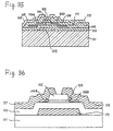
- a further problem is that as shown in Figure 36, the semiconductor layer 104 and source electrode 107 are located excessively near to each other with only the interposition of one end of the channel protective layer 105. Likewise, the semiconductor layer 104 and drain electrode 108 are located excessively near to each other with only the interposition of the other end of the channel protective layer 105. As a result, an electric leakage is likely to occur between the source electrode 107 and drain electrode 108, thereby causing a malfunction in the display operation. The leakage tends to occur and continue in the area indicated by the arrow in Figure 36 because of the non-presence of contact layers 106a and 106b in this area.
- a large-capacity active matrix display device for use in a high definition (ED) TV set, a graphic display device, and the like has been developed and used.
- the known TFTs can not be used for such large-capacity active matrix display devices in that an electric leakage of 10 ⁇ 9 to 10 ⁇ 11 A occurs.
- Japanese Patent Laid-Open Publication No. 3-4566 discloses a TFT having a structure in which contact layers having a distribution of impurities of low concentration are formed by injecting ions between the semiconductor layer and the source electrode, and between the semiconductor layer and the drain electrode.
- This TFT structure advantageously removes non-linear currents occurring by contact between the electrodes constituting the source area or drain area of the transistor and the semiconductor layer, and an off-current generated by the flow of electrons and holes caused by the irradiating of the semiconductor layer. This shortens the channel of the TFT, but on the other hand, the number of processes and photomasks are increased, thereby reducing production yield and reliability.
- the method for producing an active matrix substrate of this invention which overcomes the above-discussed and numerous other disadvantages and deficiencies of the prior art, wherein the active matrix substrate uses a thin film transistor having a gate electrode on an insulating substrate covered with a gate insulating layer, a semiconductor layer on the gate insulating layer, a channel protective layer on the semiconductor layer, a drain electrode having a portion overlying the gate electrode with the interposition of the gate insulating layer, the semiconductor layer and the channel protective layer, and a source electrode having a portion overlying the gate electrode with the interposition of the gate insulating layer, the semiconductor layer and the channel protective layer, the method comprising the steps of patterning the channel protective layer, injecting ions into the semiconductor layer through a resist remaining after the patterning formation of the channel protective layer, so as to form a contact layer.
- the contact layer is formed by patterning the semiconductor layer.
- the resist is formed on the channel protective layer by patterning and ions are injected into the semiconductor layer through the resist, and the resist lifts off to form the drain electrode and source electrode in patterns.
- the thin film transistor has a gate electrode on an insulating substrate covered with a gate insulating layer, a semiconductor layer on the gate insulating layer, a drain electrode having a portion overlying the gate electrode with the interposition of the gate insulating layer and the semiconductor layer, and a source electrode having a portion overlying the gate electrode with the interposition of the gate insulating layer and the semiconductor layer, the method comprising the steps of patterning a resist on the semiconductor layer, injecting ions into the semiconductor layer through the resist, so as to form a contact layer, forming an electroconductive layer used for the drain electrode and source electrode without removing the resist, and lifting off the resist to form the drain electrode and source electrode separately.
- the thin film transistor having a gate electrode on an insulating substrate covered with a gate insulating layer, a semiconductor layer on the gate insulating layer, a channel protective layer on the semiconductor layer, a drain electrode having a portion everlying the gate electrode with the interposition of the gate insulating layer, the semiconductor layer and the channel protective layer, and a source electrode having a portion overlying the gate electrode with the interposition of the gate insulating layer, the semiconductor layer and the channel protective layer, the method comprising the steps of patterning the channel protective layer, injecting ions into the semiconductor layer by use of the patterned channel protective layer as a mask, so as to form a contact layer.
- the contact layer is formed by injecting ions at an accelerating voltage so that impurities do not reach the gate insulating layer.
- the ions are injected such that the contact layer has the same thickness as that of the semiconductor layer.
- the thin film transistor has a gate electrode on an insulating substrate covered with a gate insulating layer, a semiconductor layer on the gate insulating layer, a channel protective layer on the semiconductor layer, a drain electrode having a portion overlying the gate electrode with the interposition of the gate insulating layer, the semiconductor layer and the channel protective layer, and a source electrode having a portion overlying the gate electrode with the interposition of the gate insulating layer, the semiconductor layer and the channel protective layer, the method comprising the steps of forming the channel protective layer in a shape having reclining sides toward the source electrode and the drain electrode, and injecting ions into the semiconductor layer through the channel protective layer such that the contact layer is formed in the portions of the semiconductor layer which are directly below the foot of the reclining sides of the channel protective layer.
- the thin film transistor has a gate electrode on an insulating substrate covered with a gate insulating layer, a semiconductor layer on the gate insulating layer, a channel protective layer on the semiconductor layer, a drain electrode having a portion overlying the gate electrode with the interposition of the gate insulating layer, the semiconductor layer and the channel protective layer, and a source electrode having a portion overlying the gate electrode with the interposition of the gate insulating layer, the semiconductor layer and the channel protective layer, the method comprising the steps of forming the channel protective layer by patterning, and injecting ions diagonally from above with respect to the substrate into the semiconductor layer having an injected protective layer to form a contact layer in an area below the channel protective layer extending from the opposite ends of the semiconductor layer up to an area located inward of the opposite ends of the channel protective layer.
- the thin film transistor has a gate electrode on an insulating substrate covered with a gate insulating layer, a semiconductor layer on the gate insulating layer, a channel protective layer on the semiconductor layer, a drain electrode having a portion overlying the gate electrode with the interposition of the gate insulating layer, the semiconductor layer and the channel protective layer, and a source electrode having a portion overlying the gate electrode with the interposition of the gate insulating layer, the semiconductor layer and the channel protective layer, wherein the semiconductor layer has a recess at the center in the direction of the width of the gate insulating layer, the channel protective layer has a narrower width than the semiconductor layer, and thinner crosswise portions than the central portion thereof, and ions are injected into the semiconductor through the channel protective layer such that a contact layer is formed in an area extending from the opposite ends of the semiconductor layer up to an area inside of the sides of the channel protective layer.
- the thin film transistor has a gate electrode on an insulating substrate covered with a gate insulating layer, a semiconductor layer on the gate insulating layer, a channel protective layer on the semiconductor layer, a drain electrode having a portion overlying the gate electrode with the interposition of the gate insulating layer, the semiconductor layer and the channel protective layer, and a source electrode having a portion overlying the gate electrode with the interposition of the gate insulating layer, the semiconductor layer and the channel protective layer, wherein the gate insulating layer has a central recess in the direction of width such that the gate insulating layer covers the gate electrode, the semiconductor layer having a stepped portion along the profile of the gate insulating layer, the channel protective layer having a narrower width than the semiconductor layer, and thinner crosswise portions than the central portion thereof, and ions are injected into the semiconductor through the channel protective layer such that a contact layer is formed in an area extending from the opposite ends of the semiconductor layer up to an area inside of the sides of the channel protective layer.
- the thin transistor layer has a semiconductor layer having a contact region and a channel region, a gate insulating layer, a gate electrode formed on a substrate in this sequence, a source electrode and a drain electrode each kept in contact with the contact region, the source electrode and the drain electrode partly overlapping with crosswise end portions of the semiconductor layer which are wider than the gate insulating layer and the gate electrode, wherein the crosswise sides of the gate insulating layer are declined wherein the side thereof toward the gate insulating electrode has a shorter reclining surface than that of the other side thereof toward the substrate, and ions are injected into the semiconductor layer from the gate electrode such that a contact layer is formed in a portion of the semiconductor layer overlapping with at least part of the reclining sides of the gate insulating electrode and part of the semiconductor layer out of the gate insulating layer.
- the thin transistor layer has a semiconductor layer having a contact region and a channel region, a gate insulating layer, a gate electrode formed on a substrate in this sequence, a source electrode and a drain electrode each kept in contact with the contact region, the source electrode and the drain electrode partly overlapping with crosswise end portions of the semiconductor layer which are wider than the gate insulating layer and the gate electrode, wherein the gate electrode is wider than the gate insulating layer, and ions are injected into the semiconductor layer from the gate electrode such that a contact layer is formed in an area extending from portions of the semiconductor layer which are located below the crosswise ends of the gate electrode up to the opposite sides of the semiconductor layer.
- the resist is patterned by exposing the back of the gate electrode to light.
- the resist is patterned by exposing the back of the gate electrode to light, and then the channel protective layer is patterned by use of the patterned resist, and ions are injected into the semiconductor layer through the channel protective layer to form a contact layer, and the contact layer is patterned by use of a second resist, wherein the second resist is used for patterning at least one of the source electrode and the drain electrode.
- the resist used for fabricating the channel protective layer is patterned by exposing the back of the gate electrode to light, and then the channel protective layer is patterned by use of the patterned resist, and ions are injected into the semiconductor layer with the resist remaining to form a contact layer.
- the invention described herein makes possible the objectives of (1) providing a method for producing an active matrix substrate, the method ensuring that the injection of ions implants no impurities into the channel protective layer, thereby causing no electric leakage between the source electrode and the drain electrode, and (2) providing a method for producing an active matrix substrate, the method ensuring that ions are injected after a semiconductor layer is patterned to form a contact layer so that the sides of the semiconductor layer are doped with impurities, thereby ensuring that an electric leakage between the source electrode and the drain electrode is reduced even if the source electrode and the drain electrode are formed after the injection of ions.
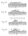
- Figures 1 to 10 are a series of sectional views showing a method for producing an active matrix substrate according to an example of the present invention.
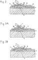
- Figure 2 is a sectional view showing the active matrix substrate produced in the process of Figure 1.
- Figures 1, 30A and 30B are showing a method for producing an active matrix substrate according to another example of the present invention.
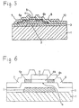
- Figures 4A and 4B are sectional views showing a method for producing an active matrix substrate according to another example of the present invention.
- Figure 5 is a sectional view showing the active matrix substrate produced by the process shown in Figure 4.
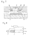
- Figure 6 is a sectional view showing an active matrix substrate produced by another method of the present invention.
- Figure 7 is a sectional view showing the production of the active matrix substrate shown in Figure 6.
- Figure 8 is an enlarged view showing a contact layer of the active matrix substrate shown in Figure 6.
- Figure 9 is a sectional view showing a contact layer produced by a known method.
- Figure 10 is a sectional view showing a contact layer of an active matrix substrate produced by a known method.
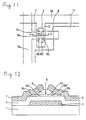
- Figure 11 is a plan view showing the active matrix substrate produced by a known method.
- Figure 12 is a sectional view taken along line A-A shown Figure 11.
- Figure 13 is a sectional view showing a method for producing the active matrix shown in Figure 11.
- Figure 14 is a plan view showing an active matrix substrate produced by another method of the present invention.
- Figure l5 is a sectional view taken along line B-B shown in Figure 14.
- Figure 16 is a sectional view showing a method for producing the active matrix substrate shown in Figure 14.
- Figure 17 is a flow chart for producing the active matrix substrate shown in Figure 14.
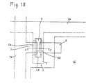
- Figure 18 is a plan view showing an active matrix substrate produced by another method of the present invention.
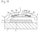
- Figure 19 is a sectional view taken along line C-C shown in Figure 18.
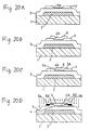
- Figures 20A to 20D are a series of sectional views showing the production method for the active matrix substrate shown in Figure 18.
- Figure 21 is a plan view showing an active matrix substrate produced by another method of the present invention.
- Figure 22 is a sectional view taken along line D-D shown in Figure 21.
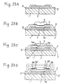
- Figures 23A to 23D are a series of the active matrix shown in Figure 21.
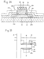
- Figure 24 is a sectional view taken along line E-E shown in Figure 25.
- Figure 25 is a plan view showing the active matrix substrate produced by another method of the present invention.
- Figure 26 is a sectional view taken along line F-F shown in Figure 27.
- Figure 27 is a plan view showing an active matrix substrate produced by another method of the present invention.
- Figures 28A and 28B are sectional views showing a method for producing the active matrix substrate by other method of the present invention.
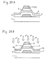
- Figures 29A and 29B are sectional views showing a continuation from Figure 28.
- Figures 30A and 30B are sectional views showing a continuation from Figure 29.
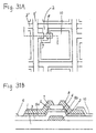
- Figure 31A is a plan view showing the active matrix substrate produced in the process of Figures 28 to 30.
- Figure 31B is a sectional view taken along line I-I in Figure 31A.
- Figures 32A and 32B are sectional views showing a method for producing a conventional active matrix substrate.
- Figure 33 is a sectional view showing the conventional active matrix substrate produced in the process shown in Figure 32.
- Figures 34A and 32B are sectional views showing a method for producing another conventional active matrix substrate.
- Figure 35 is a sectional view showing another conventional active matrix substrate produced in the process shown in Figure 34.
- Figure 36 is a sectional view used for describing the problems of the prior art.
- This example is directed to the enhancement of the transistor characteristics of an active matrix substrate.
- Ta is laminated on a transparent insulating substrate 1 such as a glass panel by a sputtering method to a thickness of 200 nm to 400 nm, preferably 300 nm. Then, a photomask is formed on the Ta layer and patterned to obtain a gate electrode 2.
- a plasma CVD method is applied to stack a gate insulating layer 3 made of SiNx having a thickness of 200 nm to 400 nm, preferably 300 nm, a semiconductor layer 4 made of amorphous silicon (hereinafter referred to "a-Si") having a thickness of 20 nm to 50 nm, preferably 30 nm, and a channel protective layer 5 made of SiNx having a thickness of 100 nm to 300 nm, preferably 200 nm in this sequence on the whole surface of the glass substrate 1 so as to cover the gate electrode 2.
- a-Si amorphous silicon
- a resist 11 is coated on the channel protective layer 5 disposed on the top surface and a photolithographic process is applied thereto using a pattern of a-Si, then the semiconductor layer 4 and the channel protective layer 5 shown in Figure 1B are patterned. After that, the resist 11 is formed on the portion of the gate insulating layer 3 which is not covered by the semiconductor layer 4 and the channel layer 5.
- a transparent electrode made of Indium tin oxidized layer (ITO) is laminated on the whole substrate 1 with a thickness of 50 nm to 100 nm, preferably 80 nm, and patterned by use of photomask to form a pixel electrode 10, thereby forming the active matrix substrate of this example.
- the present invention can be similarly applied to the thin transistor having a structure without the channel protective layer 5.
- the source electrode 7 and the drain electrode 8 can be also formed by the following method.
- the resist 11 is formed on the channel protective layer 5 over the whole substrate 1, as shown in Figure 1D, and a metal layer 13 made of Ti or Mo with a thickness of 200 nm to 400 nm is formed thereon so as to cover the above-mentioned contact layers 6a and 6b.
- the source electrode 7 and the drain electrode 8, as shown in the Figure 3B, are formed by lifting off the above-mentioned resist 11 of the metal layer 13.
- the patterning process can be omitted. Accordingly, the number of steps and the producing time is shortened, thereby giving a simplified and efficient producing process. This process may be applied to the case when the formation of the channel protective layer 5 is omitted.
- This example also is directed to a method or producing an active matrix substrate having excellent transistor characteristics. More particularly, this example discloses a producing method which is effective in the case where the injection is performed using the channel protective layer as a mask.
- Figures 4A and 4B show such a method for producing an active matrix substrate.
- the active matrix shown in Figure 5 is formed by the process described below.
- Ta is laminated on the transparent insulating substrate 1 such as a glass substrate by a sputtering method to have a thickness of 200 nm to 400 nm, preferably 300 nm. Then, a photomask is formed thereon and patterned to obtain a gate electrode 2.
- the semiconductor layer 4 is patterned as shown in Figure 4B and the contact layers 6a and 6b are formed by injection of P+ ion to the semiconductor layer 4 from the side of the channel protective layer 5.
- accelerating voltage of ion is arranged not to reach the gate insulating layer 3.
- the value of the accelerating voltage is varied in accordance with a thickness of the semiconductor layer 4. For example, when the thickness of the semiconductor layer 4 is 30 nm, which is the minimum value of this example, the value is set to be around 30 kV.
- the channel protective layer 5 is treated by a surface cleaning treatment with, for example, buffered HF (etching buffer solution which is a mixture of hydrogen fluoride and ammonium fluoride) to eliminate the damaged portion 50.
- buffered HF etching buffer solution which is a mixture of hydrogen fluoride and ammonium fluoride
- a metal layer made of Ti or Mo is formed with a thickness of 200 nm to 400 nm, preferably 300 nm, by the sputtering method on the whole surface of the substrate 1.
- the metal layer is patterned by the use of a photomask to form the source electrode 7 and the drain electrode 8 shown in Figure 5, thereby obtaining a thin transistor.
- the transparent electrode made of Indium tin oxidized layer (ITO) is laminated to a thickness of 50 nm to 100 nm, preferably 80 nm, on the whole surface of the substrate 1 and patterned by the use of a photomask to form a pixel electrode 10, thereby forming the active matrix of the present invention.
- ITO Indium tin oxidized layer
- leak of the electric current is significantly lessened, because ion is injected after the pattern formation of the semiconductor layer 4, impurities are injected on the side surface of the semiconductor layer 4, and simultaneously, the damaged portion is eliminated by cleaning with the channel protective layer 5 used as a mask. Therefore, an active matrix having excellent transistor characteristics can be obtained.
- the gate insulating layer 3 is arranged not to be reached by impurities when injecting ion, the gate insulating layer 3 may not be damaged. Therefore, threshold voltage shift does not occur, thereby attaining excellent transistor characteristics and improving the reliability as an active matrix substrate.
- This example is directed to a method for producing an active matrix which can eliminate OFF electric current using electrons and a hole as a carrier to attain excellent transistor characteristics.
- FIG. 6 shows such an active matrix.
- the active matrix substrate is produced by the process as described below.
- a gate electrode 2 is formed on the insulating substrate 1 made of a transparent glass.
- a single layer or plural layers made of Ta, Ti, Al, Cr or the like is laminated on the insulating substrate 1 by a sputtering method to have a thickness of 200 nm to 400 nm, then patterned. At this time, the gate electrode 2 is branched to form a gate bus line.
- gate insulating layer 3 and semiconductor layer 4 made of a-Si are laminated in this sequence on the insulating substrate 1 disposed the gate electrode 2.
- the gate insulating layer 3 is formed by plasma CVD method by laminating SiNx to have a thickness of 200 nm to 500 nm.
- the semiconductor layer 4 thereon contains contact layers 6a and 6b on both sides of the semiconductor layer 4a made of a-Si, which is in the center of the width direction.
- the contact layers 6a and 6b are formed by injecting ion to the semiconductor layer 4. The thickness of the contact layer is varied in accordance with the ion injection.
- the a-Si is laminated on the gate insulating layer 3, as shown in Figure 7, to have a thickness of 20 nm to 150 nm, preferably 25 nm to 100 nm and more preferably 25 nm to 50 nm, then patterned to form the semiconductor layer 4.
- a channel protective layer made of SiNx, SiO2 or the like is similarly formed with a thickness of 100 nm to 300 nm.
- impurities from Group V elements or the compound thereof, or Group III elements or the compound thereof are ion injected to the semiconductor layer 4 at the accelerating voltage 1 kV to 100 kV.
- preferable accelerating voltage for ion injection is 10 kV to 50 kV.
- both sides of the semiconductor layer 4, which are not covered with the channel protective layer 5, become contact layers 6a and 6b, into which impurities are injected at a high density. While the portion located directly below the channel protective layer 5 is separated from the channel protective layer 5, thereby attaining the original state to form semiconductor layer 4a.
- the contact layers 6a and 6b are formed throughout the semiconductor layer 4 on both sides.
- the thickness of the contact layers 6a and 6b is equal to that of the semiconductor layers 4a and 4.
- a source electrode 7 and a drain electrode 8 having one end on the channel protective layer 5 are formed on the insulating substrate 1 and disposed on the contact layers 6a and 6b as described above.
- the source electrode 7 and the drain electrode 8 are formed by lamination of a metal layer made of Ti, Al, Mo, Cr or the like to have a thickness of 200 nm to 400 nm, and patterned, thereby producing a thin transistor.
- the active matrix is produced by forming a pixel electrode electrically connected to the drain electrode 8 of the thin transistor.
- the pixel electrode is formed Indium tin oxidized layer (ITO) with a thickness of 50 nm to 100 nm.
- Figure 8 is a enlarged view of the vicinity of junction between the contact layer 6a of the active matrix and the semiconductor layer 4a formed as described above.
- thickness of the cross section of the area occupied by the vicinity of junction J is at most equal to the thickness of the semiconductor layer 4.
- the area occupied by the vicinity of junction J becomes large, if the contact layer 106a is formed by laminating semiconductor thin layer containing impurities such as Group V elements, as shown in Figure 9, or if the thickness of the contact layer which is formed by ion injection is thinner than the semiconductor layer 104, as shown in Figure 10.
- tapered channel protective layer can be used for the present invention.
- This example shows the case in which the portion of a semiconductor layer disposed directly under a channel protective layer has contact layers in order to prevent leak occurrence by separating the drain electrode and a contact layer, and the source electrode and a contact layer.
- FIG 11 is a plan view showing such an active matrix substrate and Figure 12 is a sectional view taken along line A-A.
- the active matrix substrate of this example has a gate electrode on a transparent insulating substrate 1 such as a glass substrate.
- Metals of a single layer or plural layers made of Ta, Ti, Al, Cr or the like is laminated on the transparent insulating substrate 1 with a thickness of 200 nm to 400 nm by a sputtering method, then patterned to obtain the gate electrode 2.
- a gate bus line 2a containing the gate electrode 2 branched from the gate bus line is also formed in this step (See Figure 11).
- a gate insulating layer 3 and a semiconductor layer 4 made of a-Si are formed on the substrate 1 having the gate electrode thereon.
- the gate insulating layer 3 is, for example, laminated with SiNx to have a thickness of 200 nm to 500 nm by plasma CVD method.
- Contact layers 6a and 6b, into which impurities are injected at a high density, contact layers 6a′ and 6b′, into which impurities are injected at a low density, and a semiconductor layer 4a of a-Si itself are formed on the semiconductor layer 4 located on the gate insulating layer 3. These five layers are injected with ions and formed in accordance with the injection.
- the semiconductor layer 4a is laminated on the gate insulating layer 3 with a thickness of 20 nm to 50 nm by plasma CVD method, then patterned.
- the channel protective layer 5 made of SiNx is similarly laminated on the semiconductor layer with a thickness of 100 nm to 300 nm.
- the side surface of a resist can be formed obliquely by making the backing temperature of the resist lower.
- the side surface of the channel protective layer 5 is formed obliquely with the angle ⁇ by withdrawing the side surface of the resist by dry etching to etch the channel protective layer 5.
- the etching selection ratio of the channel protective layer and the semiconductor layer must be arranged to be large.
- BHF etching buffer solution which is a mixture of hydrogen fluoride and ammonium fluoride
- the cross section of the channel protective layer 5 has the shape of a trapezoid of which the upper side is arranged to be smaller than the bottom side.
- the oblique angle ⁇ is smaller than 90°, preferably 10° to 50°. Making the side of the channel protective layer 5 oblique enables the lower layer of the channel protective layer to be thin, whereby ions are readily injected.
- the shape of the protective layer 5 is not limited to the trapezoid. A Mountain-like shape is acceptable.
- impurities of Group V elements such as P+, PH+, PH2+, B+, As ⁇ or the like and the compounds thereof, or Group III elements or the compounds thereof are injected into the semiconductor layer 4 at the accelerating voltage of 1 keV to 100 KeV, preferably 5 keV to 50 keV.
- P+ is injected.
- the portion of the semiconductor layer 4 which is not covered with the channel protective layer 5 becomes the contact layers 6a and 6b into which impurities are injected at a high density.
- a source electrode 7 and a drain electrode 8 are formed on the substrate 1 having one side on the channel protective layer 5. These source electrode 7 and drain electrode 8 have a thickness of 200 nm to 400 nm respectively and are made of Ti, Al, Mo, Cr or the like.
- the thin transistor is produced as described above.
- the active matrix substrate is formed by making pixel electrode 10 electrically connected to the drain electrode 8.
- the pixel electrode 10 is formed from an Indium tin oxidized layer (ITO) with a thickness of 50 nm to 100 nm.
- ITO Indium tin oxidized layer
- the channel protective layer 5 has contact layers 6a′ and 6b′ thereunder into which impurities are injected at a low density. Therefore, the distance between the semiconductor layer 4 and the source electrode 7, and the semiconductor layer 4 and the drain electrode 8 are separated by the presence of the contact layers 6a′ and 6b′, into which impurities are injected at a low density, thereby decreasing 1 to 2 digits of leak electric current which generated between the source electrode 7 and the drain electrode 8 to control leak occurrence.
- the active matrix substrate having a structure described above can be formed without increasing the number of processes and photomasks. As a result, the method of the present invention can be applied for the display device of an active matrix type which requires large electric current.
- This example is directed to a method for forming contact layers on a semiconductor layer disposed directly under a channel protective layer by the different way from that described in Example 4.
- FIG. 14 An active matrix substrate produced in such a method is shown in Figures 14 and 15.
- a gate bus line 2a and a source bus line 7a are disposed in the form of a grid on an insulating substrate 1 made of a transparent glass as shown in Figure 14.
- a pixel electrode 10 is disposed in the area surrounded by both lines 2a and 7a in the form of matrix. The pixel electrode 10 is necessary when used as an active matrix, but not as a thin transistor.
- the gate electrode 2 is formed in the form of projection from the gate bus line to the pixel electrode 10 and a thin transistor T is formed on the gate electrode 2.
- FIG. 15 shows the sectional structure of the thin transistor T.
- the gate electrode 2 is formed by laminating metals of a single layer or plural layers made of Ta, Ti, Al, Cr or the like on the insulating substrate 1 by a sputtering method, then patterning the metal layer.
- the gate bus line 2a is formed at the same time.
- the gate insulating layer 3 is formed on the insulating substrate 1 to cover the gate electrode 2. Then, semiconductor layer 4 made of amorphous silicon is formed.
- the gate insulating layer 3 is formed by laminating SiNx to have a thickness of 200 nm to 500 nm by the plasma CVD method.
- the semiconductor layer 4 thereon contains contact layers 6a and 6b on both sides of the semiconductor layer 4 of the central portion in the width direction. These semiconductor layer 4a and contact layers 6a an 6b are formed by injection of ions into the semiconductor layer 4, more particularly, formed in accordance with the ion injection.
- amorphous silicon is laminated on the gate insulating layer 3, for example, by plasma CVD method to the thickness of 20 nm to 50 nm, then patterned to form semiconductor layer 4.
- a channel protective layer 5 made of SiNx or the like is similarly formed with a thickness of 100 nm to 300 nm.
- the channel protective layer 5 is formed in the center of the semiconductor layer 4 to have a width smaller than that of the semiconductor layer 4.
- impurities of Group V elements such as phosphorus or compounds thereof, or Group III elements such as boron or compounds thereof are ion injected at the accelerating voltage of 1 kV to 100 kV, preferably 10 kV to 50 kV.
- the injection "from the direction of upper left side” means an injection from the side of a source electrode 7, which is formed later.
- ions are injected as describe above.
- the contact layers 6a and 6b, into which ions are injected at a low density, are formed by ion injection more than two times from both sides in the width direction of the semiconductor layer 4, which is not covered with the channel protective layer, up to the portion from the end face of the channel protective layer.
- the semiconductor layer 4 keeping the original state is formed on the rest of the portion, namely, the central portion directly under the channel protective layer 5.
- the ion injection into the insulating substrate 1 is performed with the angle of 10 to 80°, preferably 30° to 60°, more preferably 45°.
- a source electrode 7 and a drain electrode 8 are formed having one end on the channel protective layer 5.
- the source electrode and the drain electrode 8 are formed by laminating metals such as Ti, Al, Mo, Cr or the like with the thickness of 200 nm to 400 nm, and patterning.
- the source bus line 7a is formed at the same time, thereby obtaining transistor T.
- a pixel electrode 10 is formed by electrical connection to the drain electrode 8 on the insulating substrate 1.
- the pixel electrode is made of an Indium tin oxidized layer (ITO) having a thickness of 50 nm to 100 nm.
- ITO Indium tin oxidized layer
- the contact layers 6a and 6b, into which impurities are injected under the channel protective layer 5, are formed as shown in Figure 15. Therefore, the distance between the semiconductor layer 4 and the source electrode 7, and the semiconductor layer 4 and the drain electrode 8 are separated by the presence of the contact layers 6a′ and 6b′, into which impurities are injected at a low density, thereby improving the insulation therebetween, so that in the use of the active matrix of this type leak electric current generated between the source electrode 7 and drain electrode 8 can be made from 1 to 2 digits smaller to control leak occurrence.
- the active matrix substrate having a structure described above can be formed without increasing the number of processes and photomasks, thereby improving the yield rate and reliability.
- the method of the present invention can be used as a display device of an active matrix type which requires large electric current.
- This example discloses a method forming contact layer even in the portion of a semiconductor layer directly under the end of a channel protective layer by the additional method.
- Figures 18 and 19 show such an active matrix.
- a gate bus line 2a and a source bus line 7a are disposed in a grid form on the insulating substrate 1 made of transparent glass as shown in Figure 18.
- a pixel electrode 10 is disposed in the matrix form in the area surrounded by both of the bus lines 2a and 7a.
- Thin transistor T is formed on the gate electrode 2 which is formed in the form of projection in the direction from the gate bus line to the pixel electrode 10.
- Figure 19 shows the sectional structure of the thin transistor T of the active matrix.
- the gate electrode 2, the gate insulating layer 3, the semiconductor layer 4, the channel protective layer 5, the source electrode 7 and the drain electrode 8 are laminated on the insulating substrate 1 from the insulating substrate side in this sequence.
- the process of producing the active matrix substrate will be described as follows.
- metals such as Ta, Ti, Al, Cr or the like are laminated on the transparent insulting substrate 1 by sputtering method with a thickness of 200 nm to 400 nm, then patterned to form the gate electrode 2.
- the gate bus line 2a is formed at the same time.
- the gate insulating layer 3 is formed so as to cover the gate electrode 2 on the insulating substrate 1, then the semiconductor layer 4 made of amorphous silicon is formed thereon.
- the gate insulating layer 3 is formed by laminating SiNx to have a thickness of 200 nm to 400 nm, for example, by plasma CVD method.
- the semiconductor layer 4 thereon is formed as follows. First, the amorphous silicon layer is laminated with a thickness of 150 nm to 350 nm, for example, by plasma CVD method.
- the central portion of the semiconductor layer 4 is etched leaving the thickness of 50 nm to 100 nm.
- the channel protective layer 5 made of SiNx is formed in the same way in the central portion to have a thickness of 100 nm to 300 nm.
- the width of the channel protective layer 5 is arranged to be smaller than that of the semiconductor layer 4.
- the step portion generated by the concave present on the semiconductor layer 4 is leveled by etching as shown in Figure 20C. As a result, thin film layers 5a are formed on both sides of the channel protective layer 5.
- impurities of Group V elements such as phosphorus or the compound thereof, or Group III elements such as boron or the compounds thereof are ion injected at the accelerating voltage of 1 kV to 100 kV, preferably 10 kV to 50 kV.
- the contact layers 6a and 6b into which impurities are injected at a low density are formed by the injection on both sides in the width direction of the semiconductor layer 4 which is not covered with the channel protective layer 5.
- impurities are not injected into the central portion in the width direction of the semiconductor layer 4, thereby maintaining the semiconductor layer 4a in its original state.
- the source electrode 7 and the drain electrode 8 are formed having one end on the channel protective layer 5.
- metals such as Ti, Al, Mo, Cr or the like are laminated to have a thickness of 200 nm to 400 nm, then patterned.
- the source bus line 7a is formed at the same time.
- the thin transistor T is formed as described above.
- a pixel electrode 10 is formed by the electric connection to the drain electrode 8 on the insulating substrate 1 to form the active matrix substrate.
- the pixel electrode 10 is formed from an Indium tin oxidized layer (ITO) with a thickness of 50 nm to 100 nm.
- ITO Indium tin oxidized layer
- the contact layers 6a′ and 6b′ into which impurities are injected are formed under the channel protective layer 5. Therefore, the distance between the semiconductor layer 4 and the source electrode 7, and the semiconductor layer 4 and the drain electrode 8 are separated by the presence of the contact layers 6a′ and 6b′ into which impurities are injected at a low density, thereby improving the insulation therebeween. As a result, leakage (electric current leak) generated between the source electrode 7 and the drain electrode 8 can be controlled by the use of a shutter matrix produced in the process as described above.
- This example is also directed to a method forming contact layers even on the portion of a semiconductor layer directly under the end of a channel protective layer in an additional way.
- Figures 21 to 23 show such an active matrix.
- Figure 22 is a sectional view taken along the line D-D in Figure 21.
- a concave area 3a is formed in the central portion of a gate insulating layer 3 and the semiconductor layer 4 thereon is formed in the form of a step along with the channel protective layer 5.
- the contact layers 6a′ and 6b′ are formed in the portion disposed under both ends in the width direction of the channel protective layer 5 of the semiconductor layer 4.
- the thin transistor of this example has almost the same construction and producing process as the example above, so that the difference is explained as follows.
- the gate insulating layer 3′ is laminated on both sides of the gate electrode 2 as shown in Figure 23A in order to make a portion different in level from the gate insulating layer 3, thereby forming a concave portion 3a in the center of the width direction thereof.
- SiNx is laminated by plasma CVD method or SiO2 is laminated by sputtering method to have a thickness of 80 nm to 100 nm, then patterned.
- the gate insulating layer 3 and the semiconductor layer 4 made of amorphous silicon are formed in this sequence on the gate electrode 3′.
- the concave portion 3a is formed in the center in the width direction of the gate insulating layer 3 and the semiconductor layer 4 is formed in a step shape as shown.
- the gate insulating layer 3 of this example is formed by laminating SiNx with a thickness of 200 nm to 500 nm, for example, by plasma CVD method.
- the semiconductor layer 4 of this example is formed by laminating amorphous silicon with a thickness of about 20 nm to 50 nm, for example, by plasma CVD method, and patterned.
- the channel protective layer 5 is laminated with a thickness of 200 nm to 300 nm on the semiconductor layer 4, then the surface of the channel protective layer 5 is leveled in the same way by etching ( Figure 23C).
- ions are injected from the surface of the channel protective layer 5 in the same way.
- the active matrix substrate is formed by making a pixel electrode 10 in the same way.
- the electric current leak generated between the source electrode 7 and drain electrode 8 can be made 1 to 2 digits smaller.
- the active matrix substrate having a structure as described above can be formed without increasing the number of processes and photomasks, thereby improving the yield rate and reliability.
- the method can greatly contribute to producing a display device of an active matrix type which requires large electric current.
- the active matrix substrate using a thin transistor of the reverse-stagger type has been described above. However, not only this type but the active matrix substrate using thin transistor of a stagger type can be used as described as follows.
- This example is directed to a method for forming contact layers under the end portions of a gate insulating layer, on which a semiconductor layer is disposed.
- Figure 25 is a plan view of such an active matrix substrate.
- Figure 24 is a cross sectional view taken along line E-E in Figure 25.
- the semiconductor layer 22, the gate insulating layer 23 and the gate electrode 24 are disposed in this sequence on a transparent insulating substrate 21 such as glass.
- the gate insulating layer 23 has a cross section of a long trapezoid of which the upper side is smaller than the bottom side, and the side surface thereof is inclined with the oblique angle ⁇ .
- the gate electrode 24 thereon is formed such that the bottom side is equal to the upper side of the gate insulating layer 23. While the semiconductor layer 22 disposed under the gate insulating layer 23 has an upper width greater than that of the bottom side thereof.
- Contact areas 22a and 22b are formed by ion injection of impurities from both ends of the width direction of the semiconductor layer 22 to the under surface of both sides of the surface of the gate insulations 23a and 23b of the gate insulating layer 23.
- the gate electrode 24 is electrically connected to the gate electrode wiring 27 which sends signals for scanning.
- the source electrode 25a and the drain electrode 25b are formed separately in the gate insulating layer 23 from the semiconductor layer 22 to the substrate 21.
- the drain electrode 25b is electrically connected to a pixel electrode (not shown) formed by partially piling thereon. While the source electrode 25a is electrically connected to the source electrode wiring 28 for sending source signals.
- the protective layer 26 is formed over the whole surface of this substrate, thereby constructing the active matrix of this example.
- amorphous silicon is laminated on an insulation substrate 1 such as a glass to have a thickness of 20 nm to 150 nm, then patterned to form the semiconductor layer 22.
- the gate insulating layer 23 made of SiNx or the like is laminated on the semiconductor layer 22 in the same way to have a thickness of 50 nm to 500 nm.
- dry etching or wet etching is used to form the gate insulating layer 23 having the side surfaces 23a and 23b inclined.
- the oblique angle ⁇ of the side surface is less than 90°, preferably 10° to 70°, more preferably 30° to 50°.
- the thickness of the lower part of the side surfaces 23a and 23b can be made thin by inclining the surface, such that impurities can be injected into the semiconductor layer 22 disposed under both side surfaces 23a and 23b by ion injection.
- the oblique angle ⁇ of the side surfaces 23a and 23b may take different values.
- metals of a single layer or plural layers made of Ta, Ti, Al, Cr or the like is laminated on the gate insulating layer 23 by sputtering method to have a thickness of 200 nm to 400 nm, then patterned to form the gate electrode 24.
- the gate electrode 24 is produced to have the same shape and the same size as the upper surface of the insulating layer 23 located thereunder.
- impurities from Group V elements or compounds thereof, or Group III elements or the compounds thereof are ion injected to the semiconductor layer 22 at the accelerating voltage of 1 kV to 100 kV, preferably 10 kV to 50 kV.
- the contact areas 22a and 22b are formed on the portion of the semiconductor layer 22 which is not covered with the gate insulating layer 23, and of the semiconductor layer 22 which is covered with the side surface of the gate insulating layer 23.
- Impurities are injected into both layers. Impurities are not injected into the central portion of the semiconductor layer 22 covered with the gate insulating layer 23 in order to maintain the original state, thereby functioning as channel area.
- the thickness of the semiconductor layer 22, the gate insulating layer 23 and the gate electrode 24 can be determined in accordance with the ion injection of the contact areas 22a and 22b.
- a resist layer is formed in the shape of reverse-taper by dichlorobenzene treatment etc., on the gate electrode 24. After that it is laminated with Ti, Cr, Mo, Al or the like to have a thickness of 200 nm to 400 nm and lifted off, thereby forcing the source electrode 25a and the drain electrode 25b in the prescribed area on the semiconductor layer 22 and the substrate 21.
- a pixel electrode (not shown) is formed by partially piling with the drain electrode 25b to form a protective layer 26 throughout this substrate 21, thereby producing the active matrix substrate of the present invention.
- the method of the present invention can be used as a display device of the active matrix type which requires large electric current.
- the active matrix substrate can be formed without increasing the number of processes and photomasks, thereby producing an active matrix in which leak is controlled.
- amorphous silicon but also polysilicon can be used as the semiconductor layer 22.
- SiO2 can be used for the gate insulating layer 23 instead of SiNx of this example.
- a contact layer is formed under the end portion of a gate insulating layer of a semiconductor layer disposed under the gate insulating layer by a method different from Example 8.
- Figure 27 shows a plan view of such an active matrix substrate.
- Figure 26 is a cross sectional view taken along line F-F.
- the semiconductor layer 32, the gate insulating layer 33 and an gate electrode 34 are laminated in this sequence on a transparent insulating substrate to form the active matrix substrate.
- the width of each layer (line F-F direction) of the semiconductor layer 32 is greater than that of the gate insulating layer 33, and the width of each layer of the gate insulating layer 33 is greater than that of the gate electrode 34.
- Impurities are injected into contact areas 32a and 32b by ion injection.
- the contact areas 32a and 32b are formed on both sides of the semiconductor layer 32 in the width direction from the lower part of the end of gate electrode 34 to the end of the semiconductor layer 32.
- the gate electrode,34 is electrically connected to the gate electrode wiring 37 for sending scanning signals.
- a source electrode 35a and a drain electrode 35b are formed by branching the gate insulating layer 33 on the prescribed area from the semiconductor layer 32 to the substrate 31.
- the drain electrode 35b electrically connects to a pixel electrode (not shown) thereon which is formed by partially piling. While the source electrode 35a electrically connects the source electrode wiring 38 for sending source signals.
- the protective layer 36 is formed on the whole surface of the substrate 31 to construct the active matrix of this example.
- the method for producing the active matrix substrate is described as follows.
- amorphous silicon is laminated on the transparent insulating substrate 31 such as a glass to have a thickness of 20 nm to 150 nm, then patterned to form the semiconductor layer 32.
- SiNx is laminated on the semiconductor layer 32 with a thickness of 50 nm to 500 nm to form the gate insulating layer 33.
- metals such as Ta, Ti, AI, Cr or the like of a single layer or plural layers are laminated by sputtering method with the thickness of 200 nm to 400 nm, and patterned to form the gate electrode 34.
- the gate electrode 34 When patterning, the gate electrode 34 must be formed with smaller width than that of the gate insulating layer 33 thereunder. As a result, impurities can be injected into the semiconductor layer 32 disposed under the gate insulating layer 33 where the gate electrode 34 is not formed.
- impurities of Group V elements or compounds thereof, or Group III elements or the compounds thereof are ion injected into the semiconductor layer 32 at the accelerating voltage of 1 kV to 100 kV.
- contact areas 32a and 32b are formed by injection of impurities on part of the semiconductor layer 32 which is not covered with the gate insulating layer 33, and part of the semiconductor layer 32 under the gate insulating layer 33 which is not covered with the gate electrode 34.
- the central part of the semiconductor layer 32 disposed under the gate insulating layer 33 attains an original state to form the channel area.
- the thickness of the semiconductor layer 32, the gate insulating layer 33 and the gate electrode 34 can be determined in accordance with the ion injection.
- a reverse-tapered resist is formed by dichlorobenzene treatments the gate electrode 34, and laminated with Ti, Cr, Mo, Al etc., to have a thickness of 200 nm to 400 nm, then lifted off.
- the source electrode 35a and the drain electrode 35b branched by the gate insulating layer 33 are formed on the prescribed area from the semiconductor layer 32 to the substrate 31.
- a pixel electrode which is not electrically connected to the drain electrode 35b is formed by partially piling on the drain electrode 35a.
- the protective layer 36 covers the whole surface of this substrate 31, thereby forming the active matrix substrate.
- contact areas 32a and 32b into which impurities of the gate insulating layer 33 are injected to the active matrix substrate produced as described above.
- the area between the channel area and the source electrode 35a, and between the channel area and the drain electrode 35b are separated by the presence of the source electrode 35a and the drain electrode 35b, whereby the leak of electric current generated between the source electrode 35a and the drain electrode 35b can be made 1 to 2 digits smaller. Therefore, the leak occurrence can be controlled, so that the method can be used for a display device of active matrix type which requires great electric current.
- the thin transistor controlling the leak occurrence can be produced without increasing the number of the processes and photomasks.
- amorphous silicon but also polysilicon having a thickness of 50 nm to 200 nm can be used for the semiconductor layer 32.
- SiO2 can be used for the gate insulating layer 33 instead of SiNx.
- the insulating substrate is transparent, it is possible to pattern as follows.
- Figures 28, 29 and 30 are sectional views showing the method for producing an active matrix substrate.
- Figure 31 shows how the active matrix substrate is to be produced.
- Figure 31B is a section view taken along line I-I in Figure 31A.
- Ta is laminated on the glass substrate 1 by sputtering method to have a thickness of 200 nm to 400 nm, for example 300 nm.
- the gate electrode 2 is formed by the use of a photomask.
- the gate insulating layer 3 made of SiNx by plasma CVD method having a thickness of 200 nm to 500 nm, for example 300 nm, the semiconductor layer 4 made of a-Si with a thickness of 30 nm and the channel protective layer 5 with a thickness of 100 nm to 300 nm, for example 200 nm,are laminated in this sequence on the whole substrate 1 covering the gate electrode 2.
- the gate electrode 2 is exposed from the opposite side of the lamination of each layer. Namely, the exposing is performed from the back of the glass substrate 1. Since the glass substrate 1, the gate insulating layer 3, the semiconductor layer 4 and the channel protective layer 5 are exposed by the transparent light, the amount of exposure must be increased compared to the case of exposing from the upper side of the resist to obtain an appropriate light.
- Posi-resist irradiated resist dissolved by development
- the thickness of the gate electrode 2 is set to the value required for cutting the light caused by exposing from the back. In this example, the thickness is 300 nm.
- the exposed portion by the exposing from the back is dissolved by developing the resist 11, as shown in Figure 28B, thereby obtaining the prescribed shape.
- the patterned channel protective layer 5, as shown in Figure 29A, is formed by etching in the use of the resist 11.
- the resist 11 may be slightly reduced due to the etching, so that the resist 11 has a reference number 12 as well in Figure 29A to distinguish it.
- it is referred to as 12.
- the contact layers 6a and 6b are formed by injection of P+ ions without peeling the resist 12 (injection mask) from the upper side of the patterned channel protective layer 5 by the area injected P+ ion in the semiconductor layer 4.
- the resist 12 remains, because the P+ ion injection is decreased compared to the case without the resist 12, thereby lessening electrical leak generated between the source electrode 7 and the drain electrode 8, which are described later. This causes weak current between the source electrode 7 and the drain electrode 8 when P+ ions are injected into the channel protective layer 5.
- the resist 12 remains as described, the P+ ion injection into the channel protective layer 5 can be decreased compared to the case without the resist 12.
- a metal layer made of Ti or Mo is formed on the whole surface of the glass substrate 1 with a thickness of 200 nm to 400 nm, for example Mo layer electrodes 7 and 8 with a thickness of 200 nm, by sputtering method as shown in Figure 30A.
- the source electrode 7, the drain electrode 8 and the contact layers 6a and 6b are formed by patterning the metal layer and the contact layer by the use of a photomask, as shown in Figure 30B.
- the source bus line 7′ is patterned at the same time.
- the patterning is performed by a photolithographic method and the required exposure process is completed with a single exposure. Namely, exposing the coated resist by the use of photomask, then developing and patterning not only the metal layer but also the contact layer at the same time, thereby obtaining the source electrode 7 and the drain electrode 8, and the contact layers 6a and 6b.
- only one photomask exposure mask
- the position of the exposure mask is not necessary for disposing the source electrode and the drain electrode on the contact layer, which was necessary if the source electrode and the drain electrode, and the contact layer are patterned.
- the source electrode and the drain electrode, and the contact layer can be etched at the same time, for example by wet etching (mixed solution of hydrogen fluoride and nitric acid), dry etching (carbon tetrachloride group). In this example, dry etching is used, since it shows desirable accuracy. The thickness of the resist is great enough if it is over 1 ⁇ m.
- a thin transistor having the sectional construction shown in Figure 30A is formed.
- the transistor has little leakage of electric current between the source electrode 7 and the drain electrode 8, because of the small ion injection to the channel protective layer 5. Further, the transistor is difficult to be snapped, because of the presence of the contact layer 6a even under the source bus line connected to the source electrode 7.
- the transparent layer made of Indium Tin oxidized layer (ITO) is laminated on the whole surface of the glass substrate 1 on which the thin transistor is formed having a thickness of 50 nm to 100 nm, for example 80 nm, then patterned by the use of a photomask, as shown in Figure 31A, thereby forming pixel electrode 10 to obtain the active matrix substrate.
- Figure 31A shows a plan view of the active a matrix substrate and
- Figure 31B shows the sectional view taken along line I-I of the active matrix substrate.
- the thin transistor and the pixel electrode 10 are disposed in the form of matrix in accordance with the gate bus line 2′ connected to the gate electrode 2 and the source electrode 7 connected to the source bus line 7′.
- a-Si layer is used for the semiconductor layer, but polycrystal such as silicon can be also used. It is understood that the conventional material and construction of the active matrix can be applied.
- the number of photomasks and the exposure processes can be lessened, because the channel protective layer and the contact layer do not require a photomask, thereby improving the practicality. Moreover, when patterning the alignment gap can be prevented, so that an active matrix having excellent characteristics can be readily obtained.
- the contact layer is formed on the semiconductor layer by ion injection, however, the contact layer can be also formed to the same portion using another method, that is, by doping ion.
Landscapes
- Thin Film Transistor (AREA)
Applications Claiming Priority (18)
| Application Number | Priority Date | Filing Date | Title |
|---|---|---|---|
| JP408959/90 | 1990-12-28 | ||
| JP40895990A JP2694912B2 (ja) | 1990-12-28 | 1990-12-28 | アクティブマトリクス基板の製造方法 |
| JP3004575A JPH04236431A (ja) | 1991-01-18 | 1991-01-18 | アクティブマトリクス基板の製造方法 |
| JP4575/91 | 1991-01-18 | ||
| JP12004/91 | 1991-02-01 | ||
| JP3012004A JPH04247433A (ja) | 1991-02-01 | 1991-02-01 | アクティブマトリクス基板の製造方法 |
| JP3030511A JPH04269837A (ja) | 1991-02-26 | 1991-02-26 | 薄膜トランジスタの製造方法 |
| JP30511/91 | 1991-02-26 | ||
| JP3144914A JP2634505B2 (ja) | 1991-06-17 | 1991-06-17 | 薄膜トランジスタ及びその製造方法 |
| JP144914/91 | 1991-06-17 | ||
| JP21395391A JP2719252B2 (ja) | 1991-08-26 | 1991-08-26 | 薄膜トランジスタ |
| JP21395091A JP2709214B2 (ja) | 1991-08-26 | 1991-08-26 | 薄膜トランジスタの製造方法 |
| JP213953/91 | 1991-08-26 | ||
| JP213949/91 | 1991-08-26 | ||
| JP213950/91 | 1991-08-26 | ||
| JP21394991A JP2661672B2 (ja) | 1991-08-26 | 1991-08-26 | 薄膜トランジスタおよびその製造方法 |
| JP21556191A JPH0555254A (ja) | 1991-08-27 | 1991-08-27 | 薄膜トランジスタおよびその製造方法 |
| JP215561/91 | 1991-08-27 |
Publications (3)
| Publication Number | Publication Date |
|---|---|
| EP0493113A2 true EP0493113A2 (fr) | 1992-07-01 |
| EP0493113A3 EP0493113A3 (en) | 1992-09-02 |
| EP0493113B1 EP0493113B1 (fr) | 1997-03-19 |
Family
ID=33545751
Family Applications (1)
| Application Number | Title | Priority Date | Filing Date |
|---|---|---|---|
| EP91312014A Expired - Lifetime EP0493113B1 (fr) | 1990-12-28 | 1991-12-24 | Un procédé de fabrication d'un transistor à couche mince et d'un substrat à matrice active pour dispositifs de visualisation à cristaux liquides |
Country Status (3)
| Country | Link |
|---|---|
| US (1) | US5286659A (fr) |
| EP (1) | EP0493113B1 (fr) |
| DE (1) | DE69125260T2 (fr) |
Cited By (13)
| Publication number | Priority date | Publication date | Assignee | Title |
|---|---|---|---|---|
| US5286659A (en) * | 1990-12-28 | 1994-02-15 | Sharp Kabushiki Kaisha | Method for producing an active matrix substrate |
| EP0670604A3 (fr) * | 1994-03-03 | 1996-09-25 | Xerox Corp | Transistor MOS à couche mince avec une zone drain de decalage. |
| EP0766296A3 (fr) * | 1995-09-29 | 1998-05-13 | Sony Corporation | Méthode de fabrication d'un transistor à couches minces |
| EP0911872A3 (fr) * | 1997-10-24 | 1999-11-17 | Lüder, Ernst, Prof. Dr.-Ing. habil. | Méthode de fabrication de transistors à couche mince |
| GB2415542A (en) * | 2004-06-25 | 2005-12-28 | Lg Philips Lcd Co Ltd | Thin film transistor array substrate |
| FR2873826A1 (fr) * | 2004-07-30 | 2006-02-03 | Lg Philips Lcd Co Ltd | Substrat de matrice pour un ecran a cristaux liquides et procede de fabrication de ce dernier |
| US7026194B2 (en) | 1999-09-17 | 2006-04-11 | Semiconductor Energy Laboratory Co., Ltd. | Method of forming thin film transistors having tapered gate electrode and curved insulating film |
| US7223666B2 (en) | 1996-10-31 | 2007-05-29 | Semiconductor Energy Laboratory Co., Ltd. | Semiconductor device that includes a silicide region that is not in contact with the lightly doped region |
| US8017456B2 (en) | 2000-01-26 | 2011-09-13 | Semiconductor Energy Laboratory Co., Ltd. | Semiconductor device and manufacturing method thereof |
| WO2013161727A1 (fr) * | 2012-04-26 | 2013-10-31 | Sony Corporation | Dispositif semi-conducteur, dispositif d'affichage, et procédé de fabrication de dispositif semi-conducteur |
| US9673223B2 (en) | 1999-11-19 | 2017-06-06 | Semiconductor Energy Laboratory Co., Ltd. | Electroluminescence display device |
| US9905702B2 (en) | 2011-09-29 | 2018-02-27 | Semiconductor Energy Laboratory Co., Ltd. | Semiconductor device and method for manufacturing the same |
| WO2019001066A1 (fr) * | 2017-06-27 | 2019-01-03 | 京东方科技集团股份有限公司 | Transistor à couches minces et son procédé de fabrication, substrat de réseau et appareil d'affichage |
Families Citing this family (36)
| Publication number | Priority date | Publication date | Assignee | Title |
|---|---|---|---|---|
| JP2794678B2 (ja) * | 1991-08-26 | 1998-09-10 | 株式会社 半導体エネルギー研究所 | 絶縁ゲイト型半導体装置およびその作製方法 |
| JP2717237B2 (ja) * | 1991-05-16 | 1998-02-18 | 株式会社 半導体エネルギー研究所 | 絶縁ゲイト型半導体装置およびその作製方法 |
| US5254480A (en) * | 1992-02-20 | 1993-10-19 | Minnesota Mining And Manufacturing Company | Process for producing a large area solid state radiation detector |
| JP3173854B2 (ja) | 1992-03-25 | 2001-06-04 | 株式会社半導体エネルギー研究所 | 薄膜状絶縁ゲイト型半導体装置の作製方法及び作成された半導体装置 |
| US5470768A (en) * | 1992-08-07 | 1995-11-28 | Fujitsu Limited | Method for fabricating a thin-film transistor |
| GB9225906D0 (en) * | 1992-12-11 | 1993-02-03 | Philips Electronics Uk Ltd | Electronic device manufacture using ion implantation |
| US5858821A (en) * | 1993-05-12 | 1999-01-12 | Micron Technology, Inc. | Method of making thin film transistors |
| JP3173926B2 (ja) | 1993-08-12 | 2001-06-04 | 株式会社半導体エネルギー研究所 | 薄膜状絶縁ゲイト型半導体装置の作製方法及びその半導体装置 |
| US6331717B1 (en) | 1993-08-12 | 2001-12-18 | Semiconductor Energy Laboratory Co. Ltd. | Insulated gate semiconductor device and process for fabricating the same |
| JPH0756184A (ja) * | 1993-08-12 | 1995-03-03 | Sharp Corp | 表示装置 |
| TW297142B (fr) | 1993-09-20 | 1997-02-01 | Handotai Energy Kenkyusho Kk | |
| DE4435461C2 (de) * | 1993-10-06 | 2001-09-20 | Micron Technology Inc N D Ges | Dünnfilmtransistor und dessen Herstellverfahren |
| US5926701A (en) * | 1994-12-21 | 1999-07-20 | Sony Electronics, Inc. | Thin film transistor fabrication technique |
| JP3331800B2 (ja) | 1995-02-08 | 2002-10-07 | エルジー フィリップス エルシーディー カンパニー リミテッド | 電子素子及びその製造方法 |
| US5539219A (en) * | 1995-05-19 | 1996-07-23 | Ois Optical Imaging Systems, Inc. | Thin film transistor with reduced channel length for liquid crystal displays |
| US6800875B1 (en) * | 1995-11-17 | 2004-10-05 | Semiconductor Energy Laboratory Co., Ltd. | Active matrix electro-luminescent display device with an organic leveling layer |
| TW439003B (en) * | 1995-11-17 | 2001-06-07 | Semiconductor Energy Lab | Display device |
| TW309633B (fr) | 1995-12-14 | 1997-07-01 | Handotai Energy Kenkyusho Kk | |
| JPH09203908A (ja) * | 1996-01-25 | 1997-08-05 | Furontetsuku:Kk | 液晶表示装置用薄膜トランジスタおよび液晶表示装置 |
| US6043507A (en) * | 1997-09-24 | 2000-03-28 | Micron Technology, Inc. | Thin film transistors and methods of making |
| DE69832162D1 (de) | 1998-07-22 | 2005-12-08 | St Microelectronics Srl | Herstellungsverfahren für ein elektronisches Bauelement, das MOS Transistoren mit salizidierten Übergängen und nicht salizidierten Widerständen enthält |
| US6246070B1 (en) * | 1998-08-21 | 2001-06-12 | Semiconductor Energy Laboratory Co., Ltd. | Semiconductor device provided with semiconductor circuit made of semiconductor element and method of fabricating the same |
| US6475836B1 (en) * | 1999-03-29 | 2002-11-05 | Semiconductor Energy Laboratory Co., Ltd. | Semiconductor device and manufacturing method thereof |
| US6370502B1 (en) * | 1999-05-27 | 2002-04-09 | America Online, Inc. | Method and system for reduction of quantization-induced block-discontinuities and general purpose audio codec |
| JP4245292B2 (ja) * | 2001-12-06 | 2009-03-25 | シャープ株式会社 | トランジスタアレイ、アクティブマトリクス基板、表示装置、並びにトランジスタアレイおよびアクティブマトリクス基板の製造方法 |
| EP1998373A3 (fr) * | 2005-09-29 | 2012-10-31 | Semiconductor Energy Laboratory Co, Ltd. | Dispositif de semi-conducteur disposant d'une couche de semi-conducteur d'oxyde et son procédé de fabrication |
| JP5303119B2 (ja) * | 2007-06-05 | 2013-10-02 | 株式会社ジャパンディスプレイ | 半導体装置 |
| JP5704790B2 (ja) * | 2008-05-07 | 2015-04-22 | キヤノン株式会社 | 薄膜トランジスタ、および、表示装置 |
| WO2011081009A1 (fr) * | 2009-12-28 | 2011-07-07 | Semiconductor Energy Laboratory Co., Ltd. | Procédé de fabrication d'un dispositif semi-conducteur |
| KR20120045178A (ko) * | 2010-10-29 | 2012-05-09 | 삼성전자주식회사 | 박막 트랜지스터 및 이의 제조 방법 |
| TWI474409B (zh) * | 2012-02-14 | 2015-02-21 | 群康科技(深圳)有限公司 | 薄膜電晶體及其製作方法及顯示器 |
| CN103247531B (zh) * | 2012-02-14 | 2016-02-17 | 群康科技(深圳)有限公司 | 薄膜晶体管及其制作方法及显示器 |
| CN103489918A (zh) * | 2012-06-08 | 2014-01-01 | 京东方科技集团股份有限公司 | 一种薄膜晶体管和阵列基板及其制造方法 |
| US9087904B2 (en) * | 2012-06-08 | 2015-07-21 | Joled Inc. | Thin-film transistor having tapered organic etch-stopper layer |
| CN103165471A (zh) | 2013-02-19 | 2013-06-19 | 京东方科技集团股份有限公司 | 薄膜晶体管及其制作方法和显示装置 |
| US20200035709A1 (en) * | 2018-07-30 | 2020-01-30 | Shenzhen China Star Optoelectronics Technology Co., Ltd. | Method for manufacturing thin-film transistor array substrate and thin-film transistor array substrate |
Family Cites Families (19)
| Publication number | Priority date | Publication date | Assignee | Title |
|---|---|---|---|---|
| EP0071244B1 (fr) * | 1981-07-27 | 1988-11-23 | Kabushiki Kaisha Toshiba | Transistor à couche mince et procédé de fabrication |
| US4404731A (en) * | 1981-10-01 | 1983-09-20 | Xerox Corporation | Method of forming a thin film transistor |
| US4394182A (en) * | 1981-10-14 | 1983-07-19 | Rockwell International Corporation | Microelectronic shadow masking process for reducing punchthrough |
| JPS60100173A (ja) * | 1983-11-07 | 1985-06-04 | セイコーインスツルメンツ株式会社 | 液晶表示装置の製造方法 |
| JPH0680685B2 (ja) * | 1986-12-29 | 1994-10-12 | 日本電気株式会社 | 薄膜トランジスタとその製造方法 |
| JPS63221678A (ja) * | 1987-03-10 | 1988-09-14 | Sharp Corp | 薄膜トランジスタの製造方法 |
| JPH0242761A (ja) * | 1988-04-20 | 1990-02-13 | Matsushita Electric Ind Co Ltd | アクティブマトリクス基板の製造方法 |
| JPH01289251A (ja) * | 1988-05-17 | 1989-11-21 | Matsushita Electric Ind Co Ltd | 薄膜トランジスターの製造方法 |
| JPH01302769A (ja) * | 1988-05-30 | 1989-12-06 | Seikosha Co Ltd | 逆スタガー型シリコン薄膜トランジスタの製造方法 |
| JPH01309379A (ja) * | 1988-06-07 | 1989-12-13 | Sumitomo Metal Ind Ltd | 薄膜半導体素子 |
| GB2220792B (en) * | 1988-07-13 | 1991-12-18 | Seikosha Kk | Silicon thin film transistor and method for producing the same |
| JPH0646640B2 (ja) * | 1988-07-13 | 1994-06-15 | 株式会社精工舎 | シリコン薄膜トランジスタおよびシリコン薄膜トランジスタの製造方法 |
| JPH06101563B2 (ja) * | 1988-07-19 | 1994-12-12 | 工業技術院長 | 薄膜電界効果トランジスタとその製造方法 |
| JP2522364B2 (ja) * | 1988-10-25 | 1996-08-07 | 日本電気株式会社 | 薄膜電界効果型トランジスタの製造方法 |
| JP2945032B2 (ja) * | 1989-07-29 | 1999-09-06 | ソニー株式会社 | 薄膜トランジスタの製法 |
| JPH03265143A (ja) * | 1990-03-15 | 1991-11-26 | Matsushita Electron Corp | 薄膜トランジスタの製造方法 |
| US5010027A (en) * | 1990-03-21 | 1991-04-23 | General Electric Company | Method for fabricating a self-aligned thin-film transistor utilizing planarization and back-side photoresist exposure |
| JPH04132231A (ja) * | 1990-09-25 | 1992-05-06 | Asahi Glass Co Ltd | 薄膜トランジスタ及びその製造方法 |
| DE69125260T2 (de) * | 1990-12-28 | 1997-10-02 | Sharp Kk | Ein Verfahren zum Herstellen eines Dünnfilm-Transistors und eines Aktive-Matrix-Substrates für Flüssig-Kristall-Anzeige-Anordnungen |
-
1991
- 1991-12-24 DE DE69125260T patent/DE69125260T2/de not_active Expired - Fee Related
- 1991-12-24 EP EP91312014A patent/EP0493113B1/fr not_active Expired - Lifetime
- 1991-12-26 US US07/813,385 patent/US5286659A/en not_active Expired - Lifetime
Cited By (26)
| Publication number | Priority date | Publication date | Assignee | Title |
|---|---|---|---|---|
| US5286659A (en) * | 1990-12-28 | 1994-02-15 | Sharp Kabushiki Kaisha | Method for producing an active matrix substrate |
| EP0670604A3 (fr) * | 1994-03-03 | 1996-09-25 | Xerox Corp | Transistor MOS à couche mince avec une zone drain de decalage. |
| EP0766296A3 (fr) * | 1995-09-29 | 1998-05-13 | Sony Corporation | Méthode de fabrication d'un transistor à couches minces |
| US7993992B2 (en) | 1996-10-31 | 2011-08-09 | Semiconductor Energy Laboratory Co., Ltd. | Semiconductor device and method of fabricating the same |
| US7223666B2 (en) | 1996-10-31 | 2007-05-29 | Semiconductor Energy Laboratory Co., Ltd. | Semiconductor device that includes a silicide region that is not in contact with the lightly doped region |
| US7622740B2 (en) | 1996-10-31 | 2009-11-24 | Semiconductor Energy Laboratory Co., Ltd. | Semiconductor device and method of fabricating the same |
| EP0911872A3 (fr) * | 1997-10-24 | 1999-11-17 | Lüder, Ernst, Prof. Dr.-Ing. habil. | Méthode de fabrication de transistors à couche mince |
| US7615825B2 (en) | 1999-09-17 | 2009-11-10 | Semiconductor Energy Laboratory Co., Ltd. | Semiconductor device having tapered gate insulating film |
| US7026194B2 (en) | 1999-09-17 | 2006-04-11 | Semiconductor Energy Laboratory Co., Ltd. | Method of forming thin film transistors having tapered gate electrode and curved insulating film |
| US7294887B2 (en) | 1999-09-17 | 2007-11-13 | Semiconductor Energy Laboratory Co., Ltd. | Semiconductor device comprising thin film transistor |
| US9673223B2 (en) | 1999-11-19 | 2017-06-06 | Semiconductor Energy Laboratory Co., Ltd. | Electroluminescence display device |
| US8017456B2 (en) | 2000-01-26 | 2011-09-13 | Semiconductor Energy Laboratory Co., Ltd. | Semiconductor device and manufacturing method thereof |
| US8513666B2 (en) | 2000-01-26 | 2013-08-20 | Semiconductor Energy Laboratory Co., Ltd. | Semiconductor device and manufacturing method thereof |
| US7586123B2 (en) | 2004-06-25 | 2009-09-08 | Lg. Display Co., Ltd. | Thin film transistor (TFT) array substrate and fabricating method thereof that protect the TFT and a pixel electrode without a protective film |
| GB2415542B (en) * | 2004-06-25 | 2008-12-10 | Lg Philips Lcd Co Ltd | Thin film transistor array substrate and fabricating method thereof |
| GB2415542A (en) * | 2004-06-25 | 2005-12-28 | Lg Philips Lcd Co Ltd | Thin film transistor array substrate |
| US7960199B2 (en) | 2004-06-25 | 2011-06-14 | Lg Display Co., Ltd. | Thin film transistor (TFT) array substrate and fabricating method thereof that protect the TFT and a pixel electrode without a protective film |
| DE102005027445B4 (de) * | 2004-06-25 | 2012-10-25 | Lg Display Co., Ltd. | Dünnschichttransistorarray-Substrat und Herstellungsverfahren für ein solches |
| FR2873826A1 (fr) * | 2004-07-30 | 2006-02-03 | Lg Philips Lcd Co Ltd | Substrat de matrice pour un ecran a cristaux liquides et procede de fabrication de ce dernier |
| GB2416908B (en) * | 2004-07-30 | 2007-04-11 | Lg Philips Lcd Co Ltd | Array substrate for lcd and fabrication method thereof |
| US7649581B2 (en) | 2004-07-30 | 2010-01-19 | Lg Display Co., Ltd. | Array substrate of an LCD comprising first and second gate insulating layers and method of fabricating the same |
| CN100440014C (zh) * | 2004-07-30 | 2008-12-03 | 乐金显示有限公司 | 液晶显示器的阵列基板及其制造方法 |
| US9905702B2 (en) | 2011-09-29 | 2018-02-27 | Semiconductor Energy Laboratory Co., Ltd. | Semiconductor device and method for manufacturing the same |
| WO2013161727A1 (fr) * | 2012-04-26 | 2013-10-31 | Sony Corporation | Dispositif semi-conducteur, dispositif d'affichage, et procédé de fabrication de dispositif semi-conducteur |
| WO2019001066A1 (fr) * | 2017-06-27 | 2019-01-03 | 京东方科技集团股份有限公司 | Transistor à couches minces et son procédé de fabrication, substrat de réseau et appareil d'affichage |
| US11784258B2 (en) | 2017-06-27 | 2023-10-10 | Boe Technology Group Co., Ltd. | Thin film transistor with insulating portion between source/drian electrode and gate insulating layer, and manufacturing method thereof |
Also Published As
| Publication number | Publication date |
|---|---|
| DE69125260T2 (de) | 1997-10-02 |
| EP0493113B1 (fr) | 1997-03-19 |
| EP0493113A3 (en) | 1992-09-02 |
| US5286659A (en) | 1994-02-15 |
| DE69125260D1 (de) | 1997-04-24 |
Similar Documents
| Publication | Publication Date | Title |
|---|---|---|
| US5286659A (en) | Method for producing an active matrix substrate | |
| US5474941A (en) | Method for producing an active matrix substrate | |
| EP0304657B1 (fr) | Cellule matricielle active et son procédé de fabrication | |
| US4864376A (en) | Thin-film transistor and method of fabricating the same | |
| US4958205A (en) | Thin film transistor array and method of manufacturing the same | |
| KR100699987B1 (ko) | 높은 캐패시턴스를 갖는 평판표시소자 및 그의 제조방법 | |
| US6329672B1 (en) | Thin film transistor having a second gate metal layer preventing formation of hillocks | |
| JPH09292632A (ja) | アクティブマトリックス液晶表示装置のマトリックスアレイ及び液晶表示装置並びにその製造方法 | |
| EP1596637A1 (fr) | Element electroluminescent organique et son procede de production | |
| US8350994B1 (en) | Method of manufacturing a liquid crystal display | |
| US5751020A (en) | Structure of a liquid crystal display unit having exposed channel region | |
| US5166086A (en) | Thin film transistor array and method of manufacturing same | |
| US5198377A (en) | Method of manufacturing an active matrix cell | |
| JP4166300B2 (ja) | 液晶表示装置の製造方法 | |
| US5736436A (en) | Method of making a thin film transistor panel | |
| US5523865A (en) | Liquid-crystal display top gate thin film transistor with particular connection between the drain and the display electrode | |
| JPH0954342A (ja) | アクティブマトリクス液晶表示パネル及びその製造方法 | |
| KR20010110139A (ko) | 개량된 프로세스 윈도우를 구비한 완전 셀프-얼라인된tft를 형성하는 방법 | |
| JPH06326314A (ja) | 薄膜トランジスタおよびその製造方法 | |
| US7663143B2 (en) | Thin film transistor having a short channel formed by using an exposure mask with slits | |
| US5652159A (en) | Thin film transistor having improved switching characteristic | |
| EP0544069B1 (fr) | Panneau de transistor à couches minces et sa méthode de fabrication | |
| KR950003939B1 (ko) | 액티브매트리스 기판의 제조 방법 | |
| KR100218578B1 (ko) | 액정표시장치의 구조와 그 제조방법 | |
| JP2630195B2 (ja) | 薄膜電界効果トランジスタとその製造方法 |
Legal Events
| Date | Code | Title | Description |
|---|---|---|---|
| PUAI | Public reference made under article 153(3) epc to a published international application that has entered the european phase |
Free format text: ORIGINAL CODE: 0009012 |
|
| AK | Designated contracting states |
Kind code of ref document: A2 Designated state(s): DE FR GB NL |
|
| PUAL | Search report despatched |
Free format text: ORIGINAL CODE: 0009013 |
|
| AK | Designated contracting states |
Kind code of ref document: A3 Designated state(s): DE FR GB NL |
|
| 17P | Request for examination filed |
Effective date: 19921102 |
|
| 17Q | First examination report despatched |
Effective date: 19940704 |
|
| GRAG | Despatch of communication of intention to grant |
Free format text: ORIGINAL CODE: EPIDOS AGRA |
|
| GRAH | Despatch of communication of intention to grant a patent |
Free format text: ORIGINAL CODE: EPIDOS IGRA |
|
| GRAH | Despatch of communication of intention to grant a patent |
Free format text: ORIGINAL CODE: EPIDOS IGRA |
|
| GRAA | (expected) grant |
Free format text: ORIGINAL CODE: 0009210 |
|
| AK | Designated contracting states |
Kind code of ref document: B1 Designated state(s): DE FR GB NL |
|
| REF | Corresponds to: |
Ref document number: 69125260 Country of ref document: DE Date of ref document: 19970424 |
|
| ET | Fr: translation filed | ||
| PLBE | No opposition filed within time limit |
Free format text: ORIGINAL CODE: 0009261 |
|
| STAA | Information on the status of an ep patent application or granted ep patent |
Free format text: STATUS: NO OPPOSITION FILED WITHIN TIME LIMIT |
|
| 26N | No opposition filed | ||
| PGFP | Annual fee paid to national office [announced via postgrant information from national office to epo] |
Ref country code: FR Payment date: 20011212 Year of fee payment: 11 |
|
| PGFP | Annual fee paid to national office [announced via postgrant information from national office to epo] |
Ref country code: GB Payment date: 20011227 Year of fee payment: 11 |
|
| PGFP | Annual fee paid to national office [announced via postgrant information from national office to epo] |
Ref country code: NL Payment date: 20011228 Year of fee payment: 11 |
|
| REG | Reference to a national code |
Ref country code: GB Ref legal event code: IF02 |
|
| PGFP | Annual fee paid to national office [announced via postgrant information from national office to epo] |
Ref country code: DE Payment date: 20020109 Year of fee payment: 11 |
|
| PG25 | Lapsed in a contracting state [announced via postgrant information from national office to epo] |
Ref country code: GB Free format text: LAPSE BECAUSE OF NON-PAYMENT OF DUE FEES Effective date: 20021224 |
|
| PG25 | Lapsed in a contracting state [announced via postgrant information from national office to epo] |
Ref country code: NL Free format text: LAPSE BECAUSE OF NON-PAYMENT OF DUE FEES Effective date: 20030701 Ref country code: DE Free format text: LAPSE BECAUSE OF NON-PAYMENT OF DUE FEES Effective date: 20030701 |
|
| GBPC | Gb: european patent ceased through non-payment of renewal fee |
Effective date: 20021224 |
|
| NLV4 | Nl: lapsed or anulled due to non-payment of the annual fee |
Effective date: 20030701 |
|
| PG25 | Lapsed in a contracting state [announced via postgrant information from national office to epo] |
Ref country code: FR Free format text: LAPSE BECAUSE OF NON-PAYMENT OF DUE FEES Effective date: 20030901 |
|
| REG | Reference to a national code |
Ref country code: FR Ref legal event code: ST |