EP0592064B1 - Verfahren zur Herstellung eines Feldeffekttransistors - Google Patents
Verfahren zur Herstellung eines Feldeffekttransistors Download PDFInfo
- Publication number
- EP0592064B1 EP0592064B1 EP93302706A EP93302706A EP0592064B1 EP 0592064 B1 EP0592064 B1 EP 0592064B1 EP 93302706 A EP93302706 A EP 93302706A EP 93302706 A EP93302706 A EP 93302706A EP 0592064 B1 EP0592064 B1 EP 0592064B1
- Authority
- EP
- European Patent Office
- Prior art keywords
- insulating film
- gate electrode
- forming
- resist pattern
- metal layer
- Prior art date
- Legal status (The legal status is an assumption and is not a legal conclusion. Google has not performed a legal analysis and makes no representation as to the accuracy of the status listed.)
- Expired - Lifetime
Links
Images


Classifications
-
- H—ELECTRICITY
- H10—SEMICONDUCTOR DEVICES; ELECTRIC SOLID-STATE DEVICES NOT OTHERWISE PROVIDED FOR
- H10D—INORGANIC ELECTRIC SEMICONDUCTOR DEVICES
- H10D30/00—Field-effect transistors [FET]
- H10D30/01—Manufacture or treatment
- H10D30/015—Manufacture or treatment of FETs having heterojunction interface channels or heterojunction gate electrodes, e.g. HEMT
-
- H—ELECTRICITY
- H10—SEMICONDUCTOR DEVICES; ELECTRIC SOLID-STATE DEVICES NOT OTHERWISE PROVIDED FOR
- H10D—INORGANIC ELECTRIC SEMICONDUCTOR DEVICES
- H10D64/00—Electrodes of devices having potential barriers
- H10D64/01—Manufacture or treatment
- H10D64/012—Manufacture or treatment of electrodes comprising a Schottky barrier to a semiconductor
- H10D64/0124—Manufacture or treatment of electrodes comprising a Schottky barrier to a semiconductor to Group III-V semiconductors
- H10D64/0125—Manufacture or treatment of electrodes comprising a Schottky barrier to a semiconductor to Group III-V semiconductors characterised by the sectional shape, e.g. T or inverted T
-
- H—ELECTRICITY
- H10—SEMICONDUCTOR DEVICES; ELECTRIC SOLID-STATE DEVICES NOT OTHERWISE PROVIDED FOR
- H10D—INORGANIC ELECTRIC SEMICONDUCTOR DEVICES
- H10D64/00—Electrodes of devices having potential barriers
- H10D64/20—Electrodes characterised by their shapes, relative sizes or dispositions
- H10D64/27—Electrodes not carrying the current to be rectified, amplified, oscillated or switched, e.g. gates
- H10D64/311—Gate electrodes for field-effect devices
- H10D64/411—Gate electrodes for field-effect devices for FETs
-
- Y—GENERAL TAGGING OF NEW TECHNOLOGICAL DEVELOPMENTS; GENERAL TAGGING OF CROSS-SECTIONAL TECHNOLOGIES SPANNING OVER SEVERAL SECTIONS OF THE IPC; TECHNICAL SUBJECTS COVERED BY FORMER USPC CROSS-REFERENCE ART COLLECTIONS [XRACs] AND DIGESTS
- Y10—TECHNICAL SUBJECTS COVERED BY FORMER USPC
- Y10S—TECHNICAL SUBJECTS COVERED BY FORMER USPC CROSS-REFERENCE ART COLLECTIONS [XRACs] AND DIGESTS
- Y10S148/00—Metal treatment
- Y10S148/10—Lift-off masking
-
- Y—GENERAL TAGGING OF NEW TECHNOLOGICAL DEVELOPMENTS; GENERAL TAGGING OF CROSS-SECTIONAL TECHNOLOGIES SPANNING OVER SEVERAL SECTIONS OF THE IPC; TECHNICAL SUBJECTS COVERED BY FORMER USPC CROSS-REFERENCE ART COLLECTIONS [XRACs] AND DIGESTS
- Y10—TECHNICAL SUBJECTS COVERED BY FORMER USPC
- Y10S—TECHNICAL SUBJECTS COVERED BY FORMER USPC CROSS-REFERENCE ART COLLECTIONS [XRACs] AND DIGESTS
- Y10S148/00—Metal treatment
- Y10S148/139—Schottky barrier
-
- Y—GENERAL TAGGING OF NEW TECHNOLOGICAL DEVELOPMENTS; GENERAL TAGGING OF CROSS-SECTIONAL TECHNOLOGIES SPANNING OVER SEVERAL SECTIONS OF THE IPC; TECHNICAL SUBJECTS COVERED BY FORMER USPC CROSS-REFERENCE ART COLLECTIONS [XRACs] AND DIGESTS
- Y10—TECHNICAL SUBJECTS COVERED BY FORMER USPC
- Y10S—TECHNICAL SUBJECTS COVERED BY FORMER USPC CROSS-REFERENCE ART COLLECTIONS [XRACs] AND DIGESTS
- Y10S438/00—Semiconductor device manufacturing: process
- Y10S438/942—Masking
- Y10S438/948—Radiation resist
- Y10S438/951—Lift-off
Definitions
- the present invention relates to a method of producing a field effect transistor having a T-shaped gate electrode.
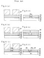
- Figures 4(a) to 4(k) are cross-sectional views illustrating process steps in a method for fabricating a prior art HEMT (High Electron Mobility Transistor) disclosed in, for example, Japanese Published Patent Application No. 63-174374 and Electronics Letters 24, 1988, p. 1327.
- HEMT High Electron Mobility Transistor
- a GaAs buffer layer 21, an intrinsic type (hereinafter referred to as i type) GaAs layer 22, an n type AlGaAs layer 23, and an n + type GaAs layer 24 are successively grown on a semi-insulating GaAs substrate (not shown) by epitaxial growth.
- an SiO 2 film is deposited on the substrate to a thickness of about 3000 ⁇ (1 ⁇ 0.1 nm), forming a first insulating film 25.
- a resist pattern 27 having an aperture of 0.5 ⁇ m (micron) width is formed on the first insulating film 25 (figure 4(a)).
- the first insulating film 25 is etched using the first resist pattern 27 as a mask to form a first aperture 25a.
- the first insulating film 25 is etched by dry etching using a mixture gas of CHF 3 and O 2 or CF 4 and O 2 .
- the n + type GaAs layer 24 is etched to form a recess 24a having a depth of about 1000 angstroms.
- the GaAs layer 24 is etched by reactive ion etching using CCl 2 F 2 or by wet etching using a mixture of tartaric acid and hydrogen peroxide solution as an etchant (figure 4(c)).
- the n + type GaAs layer 24 is etched to expose the surface of the n type AlGaAs layer 23, the etching may be stopped in the n + type GaAs layer 24.
- an SiO 2 film is deposited on the n type AlGaAs layer 23 and the first insulating film 25 to a thickness of about 3000 angstroms, forming a second insulating film 28 (figure 4(e)).
- the SiO 2 film is deposited by plasma CVD.
- the second insulating film 28 is etched in the perpendicular direction to the surface of the substrate by sputter etching or reactive ion etching, leaving portions at opposite sides of the first aperture 25a to form a second aperture 28a.
- a width w 1 of the n type AlGaAs layer 23 exposed at the bottom of the second aperture 28a is about 0.25 micron.
- a refractory metallic material 29, such as WSi is deposited on the substrate to a thickness of 1500 angstroms by sputtering, followed by annealing. Then, a low resistance metal layer 30 comprising Ti 500 angstroms thick, Pt 1000 angstroms thick, and Au 3000 angstroms thick is formed on the refractory metallic layer 29 by sputtering.
- a resist pattern 31 is formed on the low resistance metal layer 30.
- the low resistance metal layer 30 comprising Ti/Pt/Au is patterned by ion milling, and the refractory metallic layer 29 comprising WSi and the insulating film 25 comprising SiO 2 are patterned by reactive ion etching (figure 4(h)).
- the refractory metallic layer 29 and the insulating film 25 are excessively etched, so that the width of the refractory metallic layer 29 is narrower than the width of the low resistance metal layer 30.
- Figure 4(i) illustrates a case where the etching rate of the reactive ion etching is further increased. In this case, the width of the refractory metallic layer 29 is further decreased and the insulating film 25 is completely removed.
- a resist pattern for forming ohmic electrodes (not shown) is formed on the substrate, followed by a deposition of an ohmic electrode metal 32 comprising AuGe/Ni/Au and lift-off, resulting in a T-shaped gate electrode 33 and ohmic electrodes, i.e., source and drain electrodes 32a and 32B. Thereafter, the substrate is annealed at 400°C for two minutes to complete the HEMT of figure 4(k).
- the gate-to-source capacitance (Cgs) is reduced.
- the insulating film 28 remaining on opposite sides of the lower part of the T-shaped gate electrode 33 protects the surface of the n type AlGaAs layer 23.
- a crystal region in which electrons travel i.e., a region of the i type GaAs layer 22 where a two-dimensional electron gas is formed, is spaced apart from a crystal region that supplies electrons, i.e., the n type AlGaAs layer 23, by the heterojunction to prevent the electrons from being scattered by donor impurities, whereby the electron mobility of the transistor is increased.
- the HEMT in order to increase the cut-off frequency (f t ), the maximum oscillation frequency (f max ), and the unilateral gain (U) and reduce the noise factor (F o ), it is necessary reduce the gate length (Lg), the source resistance (Rs), the gate-to-source capacitance (Cgs), and the gate resistance (Rg).
- the second insulating film 28 is deposited on the substrate to fill the first aperture 25a and then etched away leaving portions on opposite side walls of the aperture 25a, which portions form a second aperture 28a having a width w 1 of 0.25 micron that would be a gate length. Thereafter, a refractory metallic material 29 is-deposited in the aperture 28a to form the lower part of the gate electrode.
- the first insulating film 25 is also etched and the thickness thereof is reduced, whereby, in the structure of figure 4(k), the interval between the over-hanging part 33a of the T-shaped gate electrode 33 and the surface of the n + type GaAs layer 24 whereon the source and drain electrodes 32a and 33b are present is reduced, resulting in an increase in the gate-to-source capacitance.
- the above-described problem can be solved by increasing the thickness of the first insulating film 25, if the thickness of the first insulating film 25 increases, the etching precision when the aperture 25a is formed in the first insulating film 25 is reduced, and the aperture 25a is not completely filled with the second insulating film 28 when the insulating film 28 is deposited on the substrate. In this case, it is difficult to form the fine aperture 28a having a width w 1 of about 0.25 micron with high controllability.
- the width w 1 of the aperture 28a at the n type AlGaAs layer 23 varies according to the thickness of the second insulating film 28 deposited in the step of figure 4(e). More specifically, the width w 1 decreases with an increase in the thickness of the second insulating film 28. When the second insulating film 28 is deposited to 3000 angstroms as described above, the width w 1 is about 0.25 micron. If the thickness of the second insulating film 28 is further increased to further reduce the gate length, the width of the V-shaped aperture 28a decreases.
- the angle of the V-shaped groove 29a formed opposite the V-shaped aperture 28a gradually decreases and the refractory metallic material 29 is not evenly deposited on the surface of the groove 29a.
- a cavity 30a is formed in the low resistance metal layer 30 deposited on the refractory metallic layer 29, which cavity increases the gate resistance.
- Japanese Published Patent Application No. 63-204772 proposes an improved method of forming a T-shaped gate structure, in which an upper metal layer of the T-shaped gate electrode is formed by a plating method using a lower metal layer of the gate electrode as a feeding electrode.
- this plating method it is difficult to apply ions onto the uneven surface, such as the surface with the V-shaped groove 29a, with keeping the ion concentration constant, so that it is impossible to grow the upper metal layer with no cavity.
- an etching stopper film is deposited, on the insulating film covering the substrate, prior to resist pattern definition and gate recess etching. It is effective to prevent the etching of the insulating film during the formation of sidewall insulation in the recess. Since, in this case, the insulating film is not etched during the sidewall formation, the thickness of this film is as deposited. The vertical distance between the overhanging portion of the T-shaped gate electrode and the source (drain) electrode is thus minimal and the cause of increased gate-to-source (drain) capacitance, i.e. insulator film erosion, has been eliminated.
- a sidewall insulation is formed in the recess, a small geometry gate length e.g. 0.5 ⁇ m or less can be achieved, if and as required.
- the etching stopper film may also be patterned to the prescribed width of the T-shaped gate electrode at the time of forming the T-shaped gate electrode. It may be of refractory metallic material, e.g. WSi, and incorporated thus as part of the gate electrode metallisation. Optionally, the sidewall insulation in the recess and A remainder of the insulating film beneath the overhanging portion of the T-shaped gate electrode may be removed to provide a further decrease in the gate-to-source (drain) capacitance.
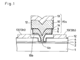
- Figure 1 is a cross-sectional view illustrating a HEMT in accordance with a first embodiment of the present invention.
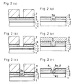
- Figures 2(a) to 2(1) are cross-sectional views illustrating process steps in a method of producing the HEMT of figure 1.
- reference numeral 1 designates a GaAs buffer layer.
- An i type GaAs layer 2 is disposed on the buffer layer 1.
- An n type AlGaAs layer 3 is disposed on the GaAs layer 2
- An n + type GaAs layer 4 is disposed on the AlGaAs layer 3.
- a recess 4a penetrates through a portion of the GaAs layer 4.
- a T-shaped gate electrode 15a is disposed on the n type AlGaAs layer 3 exposed at the bottom of the recess 4a.
- the T-shaped gate electrode 15a comprises a refractory metallic layer 9, a low resistance metal layer 10, and a metal layer 13 for ohmic electrodes.
- the ohmic electrodes i.e., source and drain electrodes 13a and 13b, are disposed on the GaAs layer 4 spaced apart from each other.
- the whole surface of this HEMT is covered with an insulating film 12 except for the metal layer 13.
- Reference numeral 14 designates a feeding metal layer.
- FIG. 2(a) there are successively grown on a semi-insulating GaAs substrate (not shown) by epitaxial growth, the GaAs buffer layer 1, the i type GaAs layer 2, the n type AlGaAs layer 3, and the n + type GaAs layer 4.
- SiO 2 is deposited on the substrate to a thickness of about 3000 angstroms by plasma CVD to form a first insulating film 5.
- WSi is deposited on the first insulating film 5 to a thickness of about 500 angstroms by sputtering to form a refractory metallic thin film 6, and a resist pattern 7 having an aperture of 0.5 micron is formed on the refractory metal thin film 6.
- the refractory metallic thin film 6 is etched by dry etching using SF 6 and the insulating film 5 is etched by dry etching using CHF 3 , CF 4 , or the like, forming a first aperture 5a.
- the n + GaAs layer 4 is etched by reactive ion etching using CCl 2 F 2 , Cl 2 , or SiCl 4 , or wet etching using a mixture of tartaric acid and hydrogen peroxide solution as an etchant, forming a recess 4a having a depth of about 1000 angstroms (figure 2(c)).
- the n + type GaAs layer 4 is etched to expose the surface of the n type AlGaAs layer 3, the etching may be stopped in the n + type GaAs layer 4.
- SiO 2 is deposited over the surface of the substrate to a thickness of 3000 to 5000 angstroms by plasma CVD, forming a second insulating film 8.
- the second insulating film 8 is etched in the vertical direction to the surface of the substrate by sputter etching or reactive ion etching, leaving portions on the opposite side walls of the first aperture 5a.
- the refractory WSi thin film 6 serves as an etching stopper layer, the thickness of the first insulating film 5 lying under the WSi thin film 6 is not reduced.
- the etching rate of a mixture gas of CHF 3 and O 2 to SiO 2 is about 500 angstroms/min, the etching rate of the gas to WSi is only 100 angstroms/min.
- a time interval required for etching the second insulating film 8 comprising SiO 2 5000 angstroms thick is 10 min
- a time interval required for etching the WSi thin film 6 500 angstroms thick is 5 min and, therefore, the first insulating film 5 is not etched even if the second insulating film 8 is excessively etched by 50 percent.
- the width w 2 of the second aperture 8a which is equivalent to a gate length, varies according to the thickness of the second insulating film 8 deposited in the step of figure 2(e). For example, when the thickness of the second insulating film 8 increases from 3000 angstroms to 5000 angstroms, the width w 2 decreases from 0.25 micron to 0.15 micron.
- a refractory metallic material such as WSi
- a refractory metallic material is deposited on the whole surface of the substrate to a thickness of about 1500 angstroms by sputtering, resulting in a refractory metallic layer 9.
- the substrate is annealed at 400 to 500°C to remove damages on the surface of the aperture 8a due to the sputtering.
- Au or the like is deposited on the refractory metallic layer 9 to a thickness of about 500 angstroms, forming a feeding metal layer 14 which serves as a feeding electrode when a metal layer is plated thereon.
- Au or the like is applied onto the feeding metal layer 14 to a thickness of about 4000 angstroms by pulse plating or electroless plating, forming a low resistance metal layer 10.
- the pulse plating and the electroless plating employed for growing the low resistance metal layer 10 have the following advantages.
- the width w 2 of the aperture 8a is narrower than 0.2 micron
- the width of the V-shaped groove 9a formed on the surface of the refractory metal layer 9 during depositing the metal layer 9 by sputtering is very narrow.
- the feeding metal layer 14 is present on the surface of the V-shaped groove 9a, when the low resistance metal layer 10 comprising Au is grown on the feeding metal layer 14, Au ions are evenly applied to the surface of the feeding metal layer 14 in the V-shaped groove 9, resulting in no cavity in the low resistance metal layer 10.
- a resist pattern 11 having a prescribed width is formed on the low resistance metal layer 10. Then, using the resist pattern 11 as a mask, the low resistance metal layer 10 and the feeding metal layer 14 are etched by ion milling, and the WSi refractory metallic layer 9, the WSi refractory metallic thin film 6, and the first insulating film 5 are etched by reactive ion etching. During the etching, the refractory metallic layers 9 and 6 and the insulating film 5 are excessively etched.
- SiO 2 is deposited on the whole surface of the structure to a thickness of 500 angstroms or less by plasma CVD, forming a third insulating film 12.
- a resist pattern (not shown) as a mask, portions of the third insulating film 12 on the top of the T-shaped gate structure 15 and on regions of the n + type GaAs layer 4 where source and drain electrodes are to be disposed are removed by reactive ion etching, followed by a deposition of an ohmic electrode metal 13 and lift-off, resulting in a T-shaped gate electrode 15a and ohmic electrodes, i.e., source and drain electrodes 13a and 13b (figure 2(1)).
- the substrate is annealed at 400°C for a few minutes to complete the HEMT of figure 1.
- the third insulating film 12 is formed in the step of figure 2(k), since the material, i.e., SiO 2 , is not sufficiently applied to the over-hanging portions 15b of the T-shaped gate structure 15, the thickness of the insulating film 12 on the over-hanging portions is very thin.
- a Ti refractory metal film may be formed in place of the WSi refractory metallic layer 9 and then the Au layer 14 is deposited to a thickness of 2000 angstroms.
- the thickness of the first insulating film 5 deposited in the step of figure 2(a) is 2000 angstroms, and the thickness of the first insulating film 25 etched in the step of figure 4(f) is 1000 angstroms.
- the interval between the over-hanging portion 15b of the T-shaped gate structure 15a and the n + type GaAs layer 4 of the HEMT of figure 1 is 1000 angstroms greater than that of the prior art HEMT because the thickness of the insulating film 5 is not reduced, whereby the capacitance beneath the over-hanging portion 15b is reduced to half of that of the prior art HEMT, resulting in a reduction in the gate-to-source capacitance.
- portions of the second insulating film 28 remain on opposite sides of the lower part of the T-shaped gate structure 33.
- the insulating film 12 as thin as or thinner than 500 angstroms is present under the T-shaped gate structure 15a, so that the dielectric constant between the over-hanging portion 15b and the n + type GaAs layer 4 is reduced as compared with that of the prior art HEMT, resulting in a further reduction in the gate-to-source capacitance Cgs.
- a high-performance HEMT with short gate length, reduced gate-to-source capacitance, and reduced gate resistance is achieved.
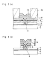
- Figures 3(a) and 3(b) are cross-sectional views illustrating process steps in a method of producing a HEMT according to a second embodiment of the present invention.
- the same reference numerals as in figures 2(a)-2(1) designate the same parts.
- a resist pattern 16 having an aperture of prescribed width is formed on the feeding metal layer 14 and then the low resistance metal layer 10 is grown on the feeding metal layer 14 by pulse plating or electroless plating (figure 3(a)).
- the feeding metal layer 14, the refractory metallic layers 6 and 9, and the first insulating film 5 are patterned to form the T-shaped gate structure 15.
- the first and second insulating films 5 and 8 are removed in the same manner as described in the first embodiment, followed by the deposition of the third insulating film 12 and the formation of the source and drain electrodes 13a and 13b. Also in this second embodiment, a high-performance HEMT with short gate length, reduced gate-to-source capacitance, and reduced gate resistance is achieved.
- the GaAs heterojunction epitaxial substrate comprising the GaAs buffer, the i type GaAs, the n type AlGaAs, and the n + GaAs
- a GaAs heterojunction epitaxial substrate for a pseudomorphic HEMT including an i type InGaAs between the i type GaAs and the n type AlGaAs may be employed.
- the epitaxial substrate may comprises other semiconductor materials, such as InP.
- HEMTs While in the above-described embodiments HEMTs are employed, the present invention may be applied to other field effect transistors.
Landscapes
- Junction Field-Effect Transistors (AREA)
Claims (6)
- Verfahren zur Herstellung eines Feldeffekttransistors, bei welchem eine T-förmige Gateelektrode (15a) und Source- und Drainelektroden (13a, 13b) auf einem epitaxialen Halbleitersubstrat (1-4) selbstjustiert angeordnet sind, mit der folgenden Sequenz von Schritten:gekennzeichnet durch:Auftragen einer ersten Isolierungsschicht (5) auf das epitaxiale Halbleitersubstrat (1-4);Bilden einer ersten Resiststruktur (7), welche eine Öffnungsstruktur einer vorgeschriebenen Breite aufweist, auf der ersten Isolierungsschicht (5);Bilden einer ersten Öffnung (5a) durch Ätzen der ersten Isolierungsschicht (5) unter Verwendung der ersten Resiststruktur (7) als Maske;Entfernen der ersten Resiststruktur (7), undAuftragen einer zweiten Isolierungsschicht (8) mit einer vorgeschriebenen Dicke auf die erste Isolierungsschicht (5) und das epitaxiale Halbleitersubstrat (1-4), welches in der ersten Öffnung (5a) bloßgelegt ist;Ätzen der zweiten Isolierungsschicht (8) in einer Richtung senkrecht zu der Oberfläche des epitaxialen Halbleitersubstrats (1-4), wobei Teile (8) an gegenüberliegenden Seitenwänden der ersten Öffnung (5a) zurückbleiben, um eine zweite Öffnung (8a) in der ersten Öffnung (5a) zu erzeugen;Auftragen eines metallischen Gateelektrodenmaterials (9) und Bilden einer T-förmigen Gateelektrode (15) darauf, während wenigstens der Teil der ersten Isolierungsschicht (5) entfernt wird, welcher Gebiete des epitaxialen Halbleitersubstrats bedeckt, an welchen Source- und Drainelektroden zu bilden sind;Bilden einer zweiten Resiststruktur auf dem epitaxialen Halbleitersubstrat (1-4), wobei die zweite Resiststruktur Öffnungen gegenüberliegend den Gebieten auf dem epitaxialen Halbleitersubstrat (1-4) aufweist, an welchen Source- und Drainelektroden zu bilden sind; undAuftragen eines Ohmschen Elektrodenmetalls (13) auf die gesamte Oberfläche des epitaxialen Halbleitersubstrats (1-4) und Entfernen der zweiten Resiststruktur mit überdeckenden Teilen des Ohmschen Elektrodenmetalls (13) durch Abheben, wodurch Source- und Drainelektroden (13a, 13b) erzeugt werden;einen Schritt des Auftragens einer Ätzstoppschicht (6) eines feuerfesten metallischen Materials auf der ersten Isolierungsschicht (5), wobei der Schritt vor dem Bilden der ersten Resiststruktur (7) ausgeführt wird, wobei die durch die erste Resiststruktur bloßgelegte Ätzstoppschicht (6) durch Ätzen während des Bildens der ersten Öffnung (5a) entfernt wird und der verbleibende Teil der Ätzstoppschicht (6) wirksam ist, als Ätzstoppschicht zu wirken, um ein Ätzen der ersten Isolierungsschicht (5) während des Ätzens der zweiten Isolierungsschicht (8) zu verhindern.
- Verfahren nach Anspruch 1, dadurch gekennzeichnet, daß das metallische Gateelektrodenmaterial (9) auf die bloßgelegten Oberflächen des epitaxialen Halbleitersubstrats (1-4) und auf die Ätzstoppschicht (6) aufgetragen wird und danach das metallische Gateelektrodenmaterial (9); wobei die Ätzstoppschicht (6) und die erste Isolierungsschicht (5) in eine vorgeschriebene Breite zur Bildung der T-förmigen Gateelektrode (15) strukturiert werden.
- Verfahren nach Anspruch 2, dadurch gekennzeichnet, daß die Schritte:Auftragen einer ersten Gatemetallschicht (14) auf die gesamte Oberfläche des metallischen Gateelektrodenmaterials (9);Bilden einer zweiten Gatemetallschicht (10) auf der gesamten Oberfläche der ersten Gatemetallschicht (14) durch Pulsplattieren oder stromloses Plattieren unter Verwendung der ersten Gatemetallschicht (14) als Zuführungselektrode; undStrukturieren der ersten und zweiten Gatemetallschichten (14, 10) in einer vorgeschriebenen Breite;vor dem Strukturieren des metallischen Gateelektrodenmaterials (9), der Ätzstoppschicht (6) und der ersten Isolierungsschicht bei der Bildung der T-förmigen Gateelektrode (15) durchgeführt werden.
- Verfahren nach Anspruch 2, dadurch gekennzeichnet, daß die Schritte:Auftragen einer ersten Gatemetallschicht (14) auf die gesamte Oberfläche des metallischen Gateelektrodenmaterials (9);Bilden einer dritten Resiststruktur (16) mit einer Öffnungsstruktur einer vorgeschriebenen Breite auf dem ersten Gatemetall (14);Bilden einer zweiten Gatemetallschicht (10) auf der ersten Gatemetallschicht (14) durch Pulsplattieren oder stromloses Plattieren unter Verwendung der ersten Gatemetallschicht (14) als Zuführungselektrode; undEntfernen der dritten Resiststruktur (16);vor der Strukturierung des metallischen Gateelektrodenmaterials (9), der Ätzstoppschicht (6) und der ersten Isolierungsschicht (5) bei der Bildung der T-förmigen Gateelektroden (15) durchgeführt werden.
- Verfahren nach einem der vorausgehenden Ansprüche, dadurch gekennzeichnet, daß die Schritte:Entfernen aller Rückstände der ersten und zweiten Isolierungsschichten (5, 8); undAuftragen einer dritten Isolierungsschicht (12) auf die gesamte Oberfläche des epitaxialen Halbleitersubstrats (1-4) und die T-förmige Gateelektrode (15a);nach dem Bilden der T-förmigen Gateelektrode (15a) und vor dem Bilden der zweiten Resiststruktur durchgeführt werden; undder Teil der dritten Isolierungsschicht (12), welcher die Gebiete des epitaxialen Halbleitersubstrats (1-4) bedeckt, an welchen die Source- und Drainelektroden zu bilden sind, unter Verwendung der zweiten Resiststruktur als Maske entfernt wird.
- Verfahren nach einem der vorausgehenden Ansprüche, dadurch gekennzeichnet, daß das feuerfeste metallische Material WSi ist.
Applications Claiming Priority (2)
| Application Number | Priority Date | Filing Date | Title |
|---|---|---|---|
| JP24421792 | 1992-08-19 | ||
| JP244217/92 | 1992-08-19 |
Publications (3)
| Publication Number | Publication Date |
|---|---|
| EP0592064A2 EP0592064A2 (de) | 1994-04-13 |
| EP0592064A3 EP0592064A3 (en) | 1995-08-16 |
| EP0592064B1 true EP0592064B1 (de) | 1998-09-23 |
Family
ID=17115492
Family Applications (1)
| Application Number | Title | Priority Date | Filing Date |
|---|---|---|---|
| EP93302706A Expired - Lifetime EP0592064B1 (de) | 1992-08-19 | 1993-04-06 | Verfahren zur Herstellung eines Feldeffekttransistors |
Country Status (3)
| Country | Link |
|---|---|
| US (1) | US5358885A (de) |
| EP (1) | EP0592064B1 (de) |
| DE (1) | DE69321184T2 (de) |
Families Citing this family (32)
| Publication number | Priority date | Publication date | Assignee | Title |
|---|---|---|---|---|
| JPH03292744A (ja) * | 1990-01-24 | 1991-12-24 | Toshiba Corp | 化合物半導体装置およびその製造方法 |
| JPH0653241A (ja) * | 1992-08-03 | 1994-02-25 | Nec Corp | 電界効果トランジスタの製造方法 |
| JPH06275655A (ja) * | 1993-03-24 | 1994-09-30 | Mitsubishi Electric Corp | 半導体装置及びその製造方法 |
| JP2560993B2 (ja) * | 1993-09-07 | 1996-12-04 | 日本電気株式会社 | 化合物半導体装置の製造方法 |
| JPH0786310A (ja) * | 1993-09-20 | 1995-03-31 | Mitsubishi Electric Corp | 高融点金属ゲート電極の形成方法 |
| JP2565119B2 (ja) * | 1993-11-30 | 1996-12-18 | 日本電気株式会社 | パターン形成方法 |
| KR0161917B1 (ko) * | 1995-08-22 | 1999-02-01 | 구자홍 | 반도체소자 제조방법 |
| JP4540142B2 (ja) * | 1999-01-19 | 2010-09-08 | ルネサスエレクトロニクス株式会社 | 半導体装置の製造方法 |
| JP4584379B2 (ja) * | 1999-07-16 | 2010-11-17 | 三菱電機株式会社 | 半導体装置の製造方法 |
| US6596598B1 (en) | 2000-02-23 | 2003-07-22 | Advanced Micro Devices, Inc. | T-shaped gate device and method for making |
| US6337262B1 (en) * | 2000-03-06 | 2002-01-08 | Chartered Semiconductor Manufacturing Ltd. | Self aligned T-top gate process integration |
| DE10117741B4 (de) * | 2001-04-09 | 2008-05-21 | United Monolithic Semiconductors Gmbh | Verfahren zur Herstellung eines Halbleiter-Bauelements mit T-förmigen Kontaktelektrode |
| US6452229B1 (en) * | 2002-02-21 | 2002-09-17 | Advanced Micro Devices, Inc. | Ultra-thin fully depleted SOI device with T-shaped gate and method of fabrication |
| DE10304722A1 (de) * | 2002-05-11 | 2004-08-19 | United Monolithic Semiconductors Gmbh | Verfahren zur Herstellung eines Halbleiterbauelements |
| US20040018738A1 (en) * | 2002-07-22 | 2004-01-29 | Wei Liu | Method for fabricating a notch gate structure of a field effect transistor |
| JP4287383B2 (ja) * | 2003-05-09 | 2009-07-01 | 富士通株式会社 | レジストの加工方法及び半導体装置の製造方法 |
| KR100514526B1 (ko) * | 2003-10-08 | 2005-09-13 | 동부아남반도체 주식회사 | 반도체 소자 및 그 제조방법 |
| KR100526478B1 (ko) * | 2003-12-31 | 2005-11-08 | 동부아남반도체 주식회사 | 반도체 소자 및 그 제조방법 |
| US7045404B2 (en) * | 2004-01-16 | 2006-05-16 | Cree, Inc. | Nitride-based transistors with a protective layer and a low-damage recess and methods of fabrication thereof |
| TW200625641A (en) * | 2004-09-24 | 2006-07-16 | Koninkl Philips Electronics Nv | Field effect transistor |
| DE102005009072B4 (de) * | 2005-02-28 | 2016-12-08 | Advanced Micro Devices, Inc. | Verfahren und Vorrichtung zur Metallabscheidung durch stromloses Plattieren unter Anwendung eines Aktivierungsschemas mit einem Substraterwärmungsprozess |
| US20070105295A1 (en) * | 2005-11-08 | 2007-05-10 | Dongbuanam Semiconductor Inc. | Method for forming lightly-doped-drain metal-oxide-semiconductor (LDD MOS) device |
| DE102006022508A1 (de) * | 2006-05-15 | 2007-11-22 | United Monolithic Semiconductors Gmbh | Verfahren zur Herstellung eines Halbleiterbauelements mit einer in einer Doppelgrabenstruktur angeordneten metallischen Gateelektrode |
| CN102315262B (zh) * | 2010-07-06 | 2013-11-20 | 西安能讯微电子有限公司 | 半导体器件及其制造方法 |
| IT1401747B1 (it) * | 2010-08-02 | 2013-08-02 | Selex Sistemi Integrati Spa | Fabbricazione di transistori ad alta mobilita' elettronica con elettrodo di controllo a lunghezza scalabile |
| IT1401748B1 (it) | 2010-08-02 | 2013-08-02 | Selex Sistemi Integrati Spa | Transistori ad alta mobilita' elettronica con elettrodo di field plate |
| US10084074B1 (en) * | 2017-03-24 | 2018-09-25 | Qualcomm Incorporated | Compound semiconductor field effect transistor gate length scaling |
| CN108766888B (zh) * | 2018-06-05 | 2019-06-21 | 福建省福联集成电路有限公司 | 一种y栅半导体器件制造方法及半导体器件 |
| CN108922850B (zh) * | 2018-06-05 | 2019-10-08 | 福建省福联集成电路有限公司 | 一种y栅晶体管器件制造方法及晶体管器件 |
| CN109841677A (zh) * | 2019-03-28 | 2019-06-04 | 英诺赛科(珠海)科技有限公司 | 高电子迁移率晶体管及其制造方法 |
| US11881506B2 (en) * | 2021-07-27 | 2024-01-23 | Globalfoundries U.S. Inc. | Gate structures with air gap isolation features |
| US12520533B2 (en) * | 2021-10-27 | 2026-01-06 | Win Semiconductors Corp. | Transistor device and gate structure |
Family Cites Families (17)
| Publication number | Priority date | Publication date | Assignee | Title |
|---|---|---|---|---|
| US4536942A (en) * | 1982-12-09 | 1985-08-27 | Cornell Research Foundation, Inc. | Fabrication of T-shaped metal lines for semiconductor devices |
| IT1190294B (it) * | 1986-02-13 | 1988-02-16 | Selenia Ind Elettroniche | Una struttura di fotopolimero a multistrati (mlr) per la fabbricazione di dispositivi mesfet con gate submicrometrico e con canale incassato (recesse) di lunghezza variabile |
| JPH0797635B2 (ja) * | 1986-06-19 | 1995-10-18 | 富士通株式会社 | 半導体装置の製造方法 |
| JPS63174374A (ja) * | 1987-01-14 | 1988-07-18 | Fujitsu Ltd | 電界効果型半導体装置の製造方法 |
| JPH07118482B2 (ja) * | 1987-02-20 | 1995-12-18 | シャープ株式会社 | 半導体装置の製造方法 |
| JPS6424465A (en) * | 1987-07-20 | 1989-01-26 | Sanyo Electric Co | Manufacture of mesfet |
| JPS6459940A (en) * | 1987-08-31 | 1989-03-07 | Nec Corp | Manufacture of semiconductor device |
| US4927789A (en) * | 1988-03-30 | 1990-05-22 | Motorola, Inc. | Radio programming device with access to a remote database |
| JPH0279437A (ja) * | 1988-09-14 | 1990-03-20 | Mitsubishi Electric Corp | 半導体装置の製造方法 |
| JPH02189936A (ja) * | 1989-01-18 | 1990-07-25 | Nec Corp | 半導体装置の製造方法 |
| US5053348A (en) * | 1989-12-01 | 1991-10-01 | Hughes Aircraft Company | Fabrication of self-aligned, t-gate hemt |
| JPH03248439A (ja) * | 1990-02-26 | 1991-11-06 | Rohm Co Ltd | 化合物半導体装置の製造方法 |
| JP2952939B2 (ja) * | 1990-03-12 | 1999-09-27 | 日本電気株式会社 | 半導体装置の金属配線形成方法 |
| JP2921020B2 (ja) * | 1990-04-28 | 1999-07-19 | 日本電気株式会社 | 電界効果トランジスタおよびその製造方法 |
| JPH0493030A (ja) * | 1990-08-09 | 1992-03-25 | Seiko Epson Corp | 半導体装置およびその製造方法 |
| JPH04130619A (ja) * | 1990-09-20 | 1992-05-01 | Mitsubishi Electric Corp | 半導体装置の製造方法 |
| US5256597A (en) * | 1992-09-04 | 1993-10-26 | International Business Machines Corporation | Self-aligned conducting etch stop for interconnect patterning |
-
1993
- 1993-04-06 DE DE69321184T patent/DE69321184T2/de not_active Expired - Fee Related
- 1993-04-06 EP EP93302706A patent/EP0592064B1/de not_active Expired - Lifetime
- 1993-04-16 US US08/046,811 patent/US5358885A/en not_active Expired - Fee Related
Also Published As
| Publication number | Publication date |
|---|---|
| EP0592064A3 (en) | 1995-08-16 |
| DE69321184D1 (de) | 1998-10-29 |
| EP0592064A2 (de) | 1994-04-13 |
| US5358885A (en) | 1994-10-25 |
| DE69321184T2 (de) | 1999-05-20 |
Similar Documents
| Publication | Publication Date | Title |
|---|---|---|
| EP0592064B1 (de) | Verfahren zur Herstellung eines Feldeffekttransistors | |
| US5538910A (en) | Method of making a narrow gate electrode for a field effect transistor | |
| EP0551110B1 (de) | Verbindungshalbleiterbauelemente | |
| WO1987007765A1 (en) | Method of making a self-aligned mesfet using a substitutional gate with sidewalls and lift-off | |
| US4679311A (en) | Method of fabricating self-aligned field-effect transistor having t-shaped gate electrode, sub-micron gate length and variable drain to gate spacing | |
| JPH05326561A (ja) | 電界効果トランジスタの製造方法 | |
| EP0715346B1 (de) | Verfahren zur Herstellung eines MESFETS mit einer T-förmigen Gate-Elektrode und dadurch hergestelltes Bauelement | |
| US5471073A (en) | Field effect transistor and method for producing the field effect transistor | |
| EP0539688B1 (de) | Verbindungshalbleiterbauelement und Verfahren zu seiner Herstellung | |
| US5336626A (en) | Method of manufacturing a MESFET with an epitaxial void | |
| US5334865A (en) | MODFET structure for threshold control | |
| US4929985A (en) | Compound semiconductor device | |
| EP0436192B1 (de) | Methode zur Herstellung eines Halbleiterbauelementes mit angeschrägten Öffnungen | |
| US5231040A (en) | Method of making a field effect transistor | |
| JPH06168962A (ja) | 電界効果型半導体装置及びその製造方法 | |
| GB2286720A (en) | Field effect transistors | |
| US5843849A (en) | Semiconductor wafer etching process and semiconductor device | |
| US5726467A (en) | Multiple narrow-line-channel fet having improved noise characteristics | |
| EP0394590A2 (de) | Feldeffekttransistoren und Verfahren zur Herstellung eines Feldeffekttransistors | |
| EP0552763A2 (de) | Verbindungshalbleiteranordnung mit einem selbstjustierenden Gute und Herstellungsverfahren | |
| KR100261461B1 (ko) | 비대칭 리쎄스 구조를 갖는 화합물반도체 소자의 제조 방법 | |
| JPS6323669B2 (de) | ||
| JPH06168959A (ja) | 半導体装置及びその製造方法 | |
| JP2000174259A (ja) | 半導体素子の製造方法 | |
| JP3109097B2 (ja) | 電界効果トランジスタの製造方法およびエッチング方法 |
Legal Events
| Date | Code | Title | Description |
|---|---|---|---|
| PUAI | Public reference made under article 153(3) epc to a published international application that has entered the european phase |
Free format text: ORIGINAL CODE: 0009012 |
|
| AK | Designated contracting states |
Kind code of ref document: A2 Designated state(s): DE FR GB |
|
| PUAL | Search report despatched |
Free format text: ORIGINAL CODE: 0009013 |
|
| AK | Designated contracting states |
Kind code of ref document: A3 Designated state(s): DE FR GB |
|
| 17P | Request for examination filed |
Effective date: 19950918 |
|
| 17Q | First examination report despatched |
Effective date: 19970709 |
|
| GRAG | Despatch of communication of intention to grant |
Free format text: ORIGINAL CODE: EPIDOS AGRA |
|
| GRAG | Despatch of communication of intention to grant |
Free format text: ORIGINAL CODE: EPIDOS AGRA |
|
| GRAH | Despatch of communication of intention to grant a patent |
Free format text: ORIGINAL CODE: EPIDOS IGRA |
|
| GRAH | Despatch of communication of intention to grant a patent |
Free format text: ORIGINAL CODE: EPIDOS IGRA |
|
| GRAA | (expected) grant |
Free format text: ORIGINAL CODE: 0009210 |
|
| AK | Designated contracting states |
Kind code of ref document: B1 Designated state(s): DE FR GB |
|
| REF | Corresponds to: |
Ref document number: 69321184 Country of ref document: DE Date of ref document: 19981029 |
|
| ET | Fr: translation filed | ||
| PGFP | Annual fee paid to national office [announced via postgrant information from national office to epo] |
Ref country code: GB Payment date: 19990408 Year of fee payment: 7 |
|
| PGFP | Annual fee paid to national office [announced via postgrant information from national office to epo] |
Ref country code: FR Payment date: 19990409 Year of fee payment: 7 Ref country code: DE Payment date: 19990409 Year of fee payment: 7 |
|
| PLBE | No opposition filed within time limit |
Free format text: ORIGINAL CODE: 0009261 |
|
| STAA | Information on the status of an ep patent application or granted ep patent |
Free format text: STATUS: NO OPPOSITION FILED WITHIN TIME LIMIT |
|
| 26N | No opposition filed | ||
| PG25 | Lapsed in a contracting state [announced via postgrant information from national office to epo] |
Ref country code: GB Free format text: LAPSE BECAUSE OF NON-PAYMENT OF DUE FEES Effective date: 20000406 |
|
| GBPC | Gb: european patent ceased through non-payment of renewal fee |
Effective date: 20000406 |
|
| PG25 | Lapsed in a contracting state [announced via postgrant information from national office to epo] |
Ref country code: FR Free format text: LAPSE BECAUSE OF NON-PAYMENT OF DUE FEES Effective date: 20001229 |
|
| PG25 | Lapsed in a contracting state [announced via postgrant information from national office to epo] |
Ref country code: DE Free format text: LAPSE BECAUSE OF NON-PAYMENT OF DUE FEES Effective date: 20010201 |
|
| REG | Reference to a national code |
Ref country code: FR Ref legal event code: ST |