US5659459A - Cartridge for electronic devices including grounding pads and conductive shielding to decrease the wavelength of emitted electromagnetic radiation - Google Patents
Cartridge for electronic devices including grounding pads and conductive shielding to decrease the wavelength of emitted electromagnetic radiation Download PDFInfo
- Publication number
- US5659459A US5659459A US08/439,633 US43963395A US5659459A US 5659459 A US5659459 A US 5659459A US 43963395 A US43963395 A US 43963395A US 5659459 A US5659459 A US 5659459A
- Authority
- US
- United States
- Prior art keywords
- cartridge
- data
- microprocessor
- printer
- register
- Prior art date
- Legal status (The legal status is an assumption and is not a legal conclusion. Google has not performed a legal analysis and makes no representation as to the accuracy of the status listed.)
- Expired - Lifetime
Links
Images



Classifications
-
- G—PHYSICS
- G06—COMPUTING OR CALCULATING; COUNTING
- G06K—GRAPHICAL DATA READING; PRESENTATION OF DATA; RECORD CARRIERS; HANDLING RECORD CARRIERS
- G06K19/00—Record carriers for use with machines and with at least a part designed to carry digital markings
- G06K19/06—Record carriers for use with machines and with at least a part designed to carry digital markings characterised by the kind of the digital marking, e.g. shape, nature, code
- G06K19/067—Record carriers with conductive marks, printed circuits or semiconductor circuit elements, e.g. credit or identity cards also with resonating or responding marks without active components
- G06K19/07—Record carriers with conductive marks, printed circuits or semiconductor circuit elements, e.g. credit or identity cards also with resonating or responding marks without active components with integrated circuit chips
- G06K19/077—Constructional details, e.g. mounting of circuits in the carrier
- G06K19/0772—Physical layout of the record carrier
- G06K19/07735—Physical layout of the record carrier the record carrier comprising means for protecting against electrostatic discharge
-
- B—PERFORMING OPERATIONS; TRANSPORTING
- B41—PRINTING; LINING MACHINES; TYPEWRITERS; STAMPS
- B41J—TYPEWRITERS; SELECTIVE PRINTING MECHANISMS, i.e. MECHANISMS PRINTING OTHERWISE THAN FROM A FORME; CORRECTION OF TYPOGRAPHICAL ERRORS
- B41J29/00—Details of, or accessories for, typewriters or selective printing mechanisms not otherwise provided for
- B41J29/377—Cooling or ventilating arrangements
-
- G—PHYSICS
- G06—COMPUTING OR CALCULATING; COUNTING
- G06K—GRAPHICAL DATA READING; PRESENTATION OF DATA; RECORD CARRIERS; HANDLING RECORD CARRIERS
- G06K19/00—Record carriers for use with machines and with at least a part designed to carry digital markings
- G06K19/06—Record carriers for use with machines and with at least a part designed to carry digital markings characterised by the kind of the digital marking, e.g. shape, nature, code
- G06K19/067—Record carriers with conductive marks, printed circuits or semiconductor circuit elements, e.g. credit or identity cards also with resonating or responding marks without active components
- G06K19/07—Record carriers with conductive marks, printed circuits or semiconductor circuit elements, e.g. credit or identity cards also with resonating or responding marks without active components with integrated circuit chips
- G06K19/077—Constructional details, e.g. mounting of circuits in the carrier
-
- G—PHYSICS
- G06—COMPUTING OR CALCULATING; COUNTING
- G06K—GRAPHICAL DATA READING; PRESENTATION OF DATA; RECORD CARRIERS; HANDLING RECORD CARRIERS
- G06K19/00—Record carriers for use with machines and with at least a part designed to carry digital markings
- G06K19/06—Record carriers for use with machines and with at least a part designed to carry digital markings characterised by the kind of the digital marking, e.g. shape, nature, code
- G06K19/067—Record carriers with conductive marks, printed circuits or semiconductor circuit elements, e.g. credit or identity cards also with resonating or responding marks without active components
- G06K19/07—Record carriers with conductive marks, printed circuits or semiconductor circuit elements, e.g. credit or identity cards also with resonating or responding marks without active components with integrated circuit chips
- G06K19/077—Constructional details, e.g. mounting of circuits in the carrier
- G06K19/07737—Constructional details, e.g. mounting of circuits in the carrier the record carrier consisting of two or more mechanically separable parts
- G06K19/07741—Constructional details, e.g. mounting of circuits in the carrier the record carrier consisting of two or more mechanically separable parts comprising a first part operating as a regular record carrier and a second attachable part that changes the functional appearance of said record carrier, e.g. a contact-based smart card with an adapter part which, when attached to the contact card makes the contact card function as a non-contact card
-
- G—PHYSICS
- G06—COMPUTING OR CALCULATING; COUNTING
- G06K—GRAPHICAL DATA READING; PRESENTATION OF DATA; RECORD CARRIERS; HANDLING RECORD CARRIERS
- G06K19/00—Record carriers for use with machines and with at least a part designed to carry digital markings
- G06K19/06—Record carriers for use with machines and with at least a part designed to carry digital markings characterised by the kind of the digital marking, e.g. shape, nature, code
- G06K19/067—Record carriers with conductive marks, printed circuits or semiconductor circuit elements, e.g. credit or identity cards also with resonating or responding marks without active components
- G06K19/07—Record carriers with conductive marks, printed circuits or semiconductor circuit elements, e.g. credit or identity cards also with resonating or responding marks without active components with integrated circuit chips
- G06K19/077—Constructional details, e.g. mounting of circuits in the carrier
- G06K19/07743—External electrical contacts
-
- H—ELECTRICITY
- H05—ELECTRIC TECHNIQUES NOT OTHERWISE PROVIDED FOR
- H05K—PRINTED CIRCUITS; CASINGS OR CONSTRUCTIONAL DETAILS OF ELECTRIC APPARATUS; MANUFACTURE OF ASSEMBLAGES OF ELECTRICAL COMPONENTS
- H05K5/00—Casings, cabinets or drawers for electric apparatus
- H05K5/02—Details
- H05K5/0208—Interlock mechanisms; Means for avoiding unauthorised use or function, e.g. tamperproof
-
- H—ELECTRICITY
- H05—ELECTRIC TECHNIQUES NOT OTHERWISE PROVIDED FOR
- H05K—PRINTED CIRCUITS; CASINGS OR CONSTRUCTIONAL DETAILS OF ELECTRIC APPARATUS; MANUFACTURE OF ASSEMBLAGES OF ELECTRICAL COMPONENTS
- H05K5/00—Casings, cabinets or drawers for electric apparatus
- H05K5/02—Details
- H05K5/0256—Details of interchangeable modules or receptacles therefor, e.g. cartridge mechanisms
-
- H—ELECTRICITY
- H05—ELECTRIC TECHNIQUES NOT OTHERWISE PROVIDED FOR
- H05K—PRINTED CIRCUITS; CASINGS OR CONSTRUCTIONAL DETAILS OF ELECTRIC APPARATUS; MANUFACTURE OF ASSEMBLAGES OF ELECTRICAL COMPONENTS
- H05K7/00—Constructional details common to different types of electric apparatus
- H05K7/20—Modifications to facilitate cooling, ventilating, or heating
- H05K7/2039—Modifications to facilitate cooling, ventilating, or heating characterised by the heat transfer by conduction from the heat generating element to a dissipating body
- H05K7/20436—Inner thermal coupling elements in heat dissipating housings, e.g. protrusions or depressions integrally formed in the housing
- H05K7/20445—Inner thermal coupling elements in heat dissipating housings, e.g. protrusions or depressions integrally formed in the housing the coupling element being an additional piece, e.g. thermal standoff
Definitions
- the present invention generally relates to plug in type cartridges for providing additional or new operating features for printers and other existing electronic systems, and more particularly to a method and apparatus for minimizing extraneous electromagnetic noise generated by such cartridge devices.
- processor controlled electronic equipment are determined by the capabilities of the processor itself. That is, each processor is itself finally limited by operating characteristics such as the maximum number of processing steps obtainable per unit time, the maximum number of data bits that can be processed at one time, the width of any data or command transfer buses, and so forth.
- achieving improvements by merely upgrading software versions is at best limited to improving equipment ease of use. Realistically, it has not been possible to achieve significant improvements in operating functionality for existing electronic equipment.
- page printers such as laser printers
- the resolution of laser printers typically ranges from 240 to 800 dots per inch (dpi), and printing speed is on the order of several pages a minute.
- Such printers principally employ an electrophotographic printer element, such as a xerography unit, which uses a photo-sensitive drum as part of the printing engine. After the printer has received and stored one page of image data (or blank), image processing steps, that is, electrostatic charge, exposure, toner application, and image transfer, take place continuously in synchronization with rotation of the photo-sensitive drum.
- page printer memory capacity for image development or processing must be sufficient to store at least one page of image data at a time. If no image data compression is employed, this capacity is determined by the printer resolution being used and the page size to be accommodated. For example, if a resolution of 300 dpi and a page size of 8 by 10 inches are used, the printer may handle as much as 8 ⁇ 300 ⁇ 10 ⁇ 300 or 7,200,000 dots or pixels, of image data. If the print or image input data is in the form of a bit mapped image, the printer only needs to accept and sequentially store this data before image processing. The processing speed for this type of operation generally depends on, and is limited by, the data transfer rate. Since parallel data transfer, such as that complying with the Centronics specification standard, occurs at a considerably high rate, it is unlikely that data transfer of bit images will occur at a slower rate than the printing capability of the xerographic unit.
- printers receive and process other types of data, such as character codes, line positions, and line and character pitch, and then develop this data into a page image, or receive programs that describe the page using a page description language (PDL) and then interpret and process this information to generate a page image
- PDL page description language
- the extra image processing overhead incurred by such processing imposes a major reduction in overall printing speed. That is, the image output speed of the printer is now substantially determined, or limited, by the speed with which the processor performs image processing and memory accesses which combine to create much slower transfer rates than the xerography unit is capable of handling, resulting in a major reduction in printing capability.
- Expansion cartridge slots have a specific address, or address range or space assigned to them which is detected and read by a printer control unit after power is applied to the printer. If a cartridge containing a PDL interpreter program has been inserted, and, therefore, resides at the appropriate addresses, a pre-selected code is returned to the controller to indicate that the cartridge contains a PDL program. In this situation, control of the printer for image data developing switches to the interpreter program which is read from its address locations inside the cartridge. As a result, the printer is able to interpret received data based on the use of the particular PDL implemented by the cartridge program.
- the use of an interpreter program does not itself increase the processing speed and the overall printing speed may in fact decrease as a result of employing a high level description language with the printer processor.
- a cartridge equipped with a second microprocessor separate from that normally used by the main printer has been invented to resolve the problems described above.
- This cartridge and certain of its features are disclosed in the co-pending U.S. Patent Applications listed above which are incorporated herein by reference.
- the disclosed cartridge is able to receive print data from the printer and use its own microprocessor to process and develop image data based on stored PDL interpreters and other program data, and then provide print data back to the printer for forming the desired output image.
- any advanced microprocessor used in the cartridge comprises an electronic circuit having from tens to hundreds of thousands of components or elements, such as transistors, which operate, or switch between operating states, at frequencies of 20 MHz to 40 MHz, or higher.
- Such microprocessors typically generate substantial amounts of heat during operation, increasing the operating temperature of the microprocessor structure, and potentially generating errors or causing physical deterioration and destruction if the heat is not adequately dissipated. This situation is exasperated by operating within a very confined cartridge volume.
- the cartridge housing or casing is typically designed to maintain a maximum temperature of about 80° C.
- a maximum temperature of about 80° C.
- this type of add-on device or cartridge employs a thermally conductive housing or case typically made from aluminum which allows conduction and radiation of heat to the surrounding environment. While a conductive housing effectively intercepts electromagnetic radiation, it can also re-radiate the deposited energy if it is not re-directed to a suitable ground or fixed voltage potential. This could generate noise in, or spurious interference with, sensitive components and circuitry positioned adjacent to the housing. Depending on the method of manufacture, such housings or cases also often provide through-paths along which electromagnetic radiation can "leak" when circuits are operating at certain desired frequencies.
- one purpose of the present invention is to provide an add-on or add-in cartridge for electronic equipment which has improved electromagnetic radiation isolation.
- An advantage of the cartridge is that any transfer of undesirable electromagnetic radiation to a surrounding environment from a built in microprocessor and other circuit elements is greatly reduced.
- An additional purpose of the invention is to provide a cartridge for electronic devices which assists in efficiently cooling internal circuit elements.
- Another advantage of the invention is that a cost effective minimum complexity solution is provided for heat dissipation problems.
- an add-on or add-in electronic circuit or cartridge which is configured for insertion into a predesigned connector or receptacle in an electronic device.
- the electronic device has an insertion opening or slot for receiving the cartridge, and at least a first processor for performing certain predefined logical operations within the electronic device.
- the cartridge is provided with conductive shielding positioned around or adjacent to at least certain noise producing portions, and at least one electrical conductor or conductive element which is connected between the shielding and at least one conductive element or surface, such as an interior support frame, within the electronic device.
- a first memory in the electronic device is connected to the first processor and used to store programs or processing steps for execution by the processor.
- An address signal line is also coupled between the processor and the add-on or add-in connector.
- An address output element or controller is connected in series with the address signal line and the add-on connector which converts print and command data into address signals which are transferred to the cartridge through the connector. Therefore, a read-only address line reflects data to be processed outside of the electronic device.
- the cartridge employs a second, digital, processor which performs certain logical operations independent of those of the first processor and is preferably mounted on a circuit board.
- Conductors may also be used to electrically connect the shielding, fixed potential conductors on the circuit board, and the electronic device conductive element. This results in stabilization of any potential difference between the shielding, the circuit board, and the electronic device the cartridge is installed in, which prevents generation or transfer of electromagnetic noise resulting from currents between these elements.
- a second memory is generally used in the cartridge to store programs or steps executed by the second processor and a data fetch device that fetches or decides data reflected in the address information transferred from the electronic device connector, or address line.
- the add-in cartridge generally houses the circuit board in a case which incorporates the shielding and at least part of the case is metal with the remainder being provided with at least a layer or coating of conductive material.
- the case is generally manufactured using first and second mating case elements or shells. An overlapping ridge or shoulder is formed adjacent to the mating surfaces to preclude formation of a through-path for radiation.
- a layer of conductive material is formed on, and adjacent to, mating surfaces of at least one of the two case elements, to prevent noise producing electromagnetic radiation from escaping through the mating joint of the two case elements. This is particularly important for portions of the cartridge that may protrude from the electronic device when the cartridge is installed.
- one of the two case elements is manufactured from a plastic material, and the other from a metallic material.
- Connection elements should electrically connect conductors on the circuit board to the shielding at multiple locations to reduce any impedance between the two to effectively prevent the generation of high frequency noise. If the case is manufactured with a through-hole, such as for an electrical plug which interfaces with the electronic device, shielding connections should bridge at least one intermediate position within the through-hole. This position is typically located at a midpoint between ends of an elongated through-hole from which a corrector plug protrudes. Since the wavelength of electromagnetic radiation that can be emitted from the through-hole is reduced by this configuration, harmful electromagnetic noise at the wavelengths of interest, such as that specified in government regulations, is effectively reduced.
- connection elements may also include one or more elastically deformable conductive elements electrically connected to the shielding, which have a portion that protrudes outside of the cartridge through an opening in the case.
- the protruding elements also electrically connect to a conductive element or surface within the electronic device when the cartridge is installed.
- multiple elastic conductive elements are used to assure that at least one forms an adequate electrical connection with conductive surfaces in the electronic device.
- the multiple conductive elastic members may also electrically connect the shielding and fixed potential or power source conductors on the circuit board.
- metallic heat dissipation material is secured to the inside of the case and adjacent to a top surface of the second processor with an intervening thermal transfer element being disposed between and in contact with the two.
- an intervening thermal transfer element is disposed between and in contact with the two.
- an expansion memory connector is provided on the circuit board, along with an expansion access slot in the cartridge housing and a removable expansion slot cover.
- This configuration allows easy addition of memory as required for specific applications by simple insertion of expansion memory cards into the expansion memory connector.
- the expansion slot cover should be disposed in a position that is hidden inside the electronic device when the cartridge is inserted in the electronic device to prevent inadvertent removal or insertion of expansion memory while the cartridge is in use. Configuring the expansion memory as an Integrated Circuit of IC card greatly simplifies memory expansion.
- the cartridge By also providing the cartridge with a joining device that mechanically joins the cartridge and the main electronic device, such as to the device housing, theft of the cartridge can also be prevented.
- the joining device may also employ a locking device which incorporates an electrical switch which can be connected to the power source for the cartridge. Therefore, in this embodiment locking the cartridge in place also activates the cartridge.
- the cartridge uses an address output means that reflects the data to be transferred to the outside in an address signal and outputs the address signal via the connector, a second memory that stores the instruction to be executed by the second processor, a data fetch device that fetches data reflected in the address from the address signal output from the electronic device, a circuit board on which are mounted the second processor, the second memory and the data fetch device.
- FIG. 1 illustrates a perspective view of one embodiment of a cartridge structure constructed according to the principles of the present invention
- FIG. 2 illustrates an exploded perspective view of the cartridge of FIG. 1;
- FIG. 3 illustrates an enlarged perspective view of a printed circuit board used in the cartridge of FIG. 1;
- FIG. 4A illustrates a plan view of a lower case of the cartridge of FIG. 1;
- FIG. 4B illustrates an end view of a lower case of the cartridge of FIG. 1;
- FIG. 5 illustrates a plan view of the printed circuit board of FIG. 3 without components installed
- FIG. 6A illustrates a side view of the printed circuit board of FIG. 3 positioned above the lower case of FIG. 4;
- FIG. 6B illustrates a side view of the printed circuit board of FIG. 3 mounted in the lower case of FIG. 4;
- FIG. 7 illustrates an enlarged cross-sectional view of the cartridge of FIG. 1 showing principal parts positioned near a cartridge microprocessor
- FIG. 8 illustrates a perspective view of the cartridge of FIG. 1 inserted in one type of printer
- FIG. 9 illustrates a perspective view of the cartridge of FIG. 1 inserted in another type of printer
- FIG. 10 illustrates a longitudinal cross section of the cartridge of FIG. 1 inserted in a printer frame of a first type
- FIG. 11 illustrates a longitudinal cross section of the cartridge of FIG. 1 inserted in a printer frame of a second type
- FIG. 12A graphically illustrates electromagnetic noise measurements taken before implementing noise countermeasures
- FIG. 12B graphically illustrates electromagnetic noise measurements taken after implementing noise countermeasures
- FIG. 13 illustrates a cartridge joined to a printer using a chain
- FIG. 14 illustrates a cartridge having a keyed lock mechanism
- FIG. 15 illustrates a block diagram of the overall structure of a printer with a cartridge installed
- FIG. 16 illustrates a configuration for signal lines in a printer connector
- FIG. 17 illustrates an address map for a cartridge when viewed from the point of view of an electronic control device
- FIG. 18 illustrates an address map for a cartridge when viewed from the point of view of a cartridge microprocessor
- FIG. 19 illustrates a block diagram of a cartridge constructed according to the invention.
- FIGS. 20A, 20B, and 20C illustrate schematics of exemplary circuits useful for implementing interrupt request register 640 of FIG. 19;
- FIG. 21 illustrates a schematic of an exemplary circuit useful for implementing polling command register 643 of FIG. 19;
- FIG. 22 illustrates sample data stored in of status register 645 of FIG. 19
- FIG. 23 illustrates a schematic of an exemplary read control circuit 620 as used in FIG. 19;
- FIG. 24 illustrates a flowchart processing steps used by control circuit 501 of FIG. 19 for transferring data using read control circuit 620;
- FIG. 25 illustrates an exemplary data structure inside of a storage ROM used in the cartridge of FIG. 19;
- FIG. 26 illustrates a flowchart of processing steps performed by the cartridge of FIG. 19 for using a read control circuit 620 to transfer data
- FIG. 27 illustrates a flowchart of processing steps used by the cartridge of FIG. 19 to transfer data using a first-in-first-out or FIFO control circuit
- FIG. 28 illustrates a flowchart of processing steps performed by the cartridge of FIG. 19 for transferring data using a FIFO control circuit
- FIG. 29 illustrates a schematic of an exemplary double-bank control circuit for use in the cartridge of FIG. 19;
- FIG. 30 illustrates a flowchart of processing steps used for starting the transfer of data with the double bank control circuit of FIG. 29;
- FIG. 31 illustrates a flowchart of response processing steps executed in the printer of FIG. 15;
- FIG. 32 illustrates a flowchart of processing steps executed for transferring data using the double-bank control circuit of FIG. 29;
- FIG. 33 illustrates a flowchart of processing steps used for receiving data using the double bank control circuit of FIG. 29.
- FIG. 34 illustrates graphical representations of the timing relationships involved in printing image data by controlling the laser engine 505 of FIG. 19 with an electronic control circuit.
- Exemplary embodiments of the present invention are disclosed in relation to: the physical structure and components used; electromagnetic noise test results; alternative cartridge embodiments; overall printer and cartridge combination structure, and certain other aspects of applications of the invention.
- the present invention provides a method and apparatus for minimizing electrical noise or interference caused by the transfer of electromagnetic radiation from add-on data processing devices such as expansion cartridges for laser printers.
- the add-on device or cartridge uses a housing or casing designed to provide substantially complete electromagnetic shielding and eliminate direct transfer paths to the cartridge exterior for any radiation generated within the cartridge.
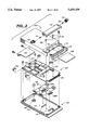
- FIG. 1 A perspective view of one embodiment of a printer-cartridge-type of add-on electronic device which is constructed and operating according to the present invention is illustrated in FIG. 1. An exploded perspective view of this cartridge is then illustrated in FIG. 2.
- the cartridge (503) illustrated in FIG. 1 is designed for insertion into an expansion slot of the type commonly found on many laser printers for adding font capabilities.
- the inventive cartridge is also able to receive print data from the printer, process and develop the received data into image data, and provide the results back to the printer for producing an output image.
- a cartridge 503 is shown having a multi-layer printed circuit board 550, called printed circuit board below, mounted inside of a generally upside-down U-shaped upper casing, shell, or housing 100 which has a recessed edge and a mating, plate-like, lower casing, shell, or housing 120.
- a cap or end cover composed of a lower cap 140 and an upper cap 150, is mounted on one side, or end, of the cartridge adjacent to a connector end of printed circuit board 550.
- a heat generating circuit element, component, or device, such as a microprocessor 601 is shown installed on printed circuit board 550.
- the cartridge end where caps 140 and 150 are located is referred to as the front of the cartridge and the opposite end of the cartridge, where the microprocessor 601 is positioned, is referred to as the rear of the cartridge.
- Upper case 100, lower cap 140, and upper cap 150 are typically made from a lightweight, easily manipulated material such as, but not limited to, ABS resin. Manufacturing the cartridge casings from non-metallic material provides a low cost advantage, for providing a less expensive case, and makes the cartridge lighter in weight and easier to transport or carry.
- Lower case 120 is typically manufactured from a lightweight metallic material such as aluminum. Aluminum is preferred because it has a high thermal conductance rate and is very effective at conducting heat to the outside of the cartridge.
- a conductive layer is formed on the inside surface of upper case 100, which together with lower case 120 constitutes a frame ground.
- An exemplary conductive or metallic material for the conductive layer on upper case 100 is electrodeless copper-nickel plating.
- the conductive layer can also be formed by using vacuum deposition of a conductive coating material, such as aluminum, or by applying a conductive paint or other liquid based coating material containing metal or conductive material.
- upper case 100 can be manufactured from a conductive plastic material which does not require a conductive coating.
- An insertion plug 551 is formed on a top or bottom surface of the front end of printed circuit board 550, and consists of a series of electrodes or contacts arranged in parallel on surfaces of the board for contacting matching electrical contacts inside the printer cartridge slot. The number of contacts is determined by the corresponding size of a matching connector conventionally provided in the printer. Connecting or insertion plug 551 may also employ orientation slots or guides, if also used in the printer.
- microprocessor 601 and other circuit elements are shown installed toward the rear of printed circuit board 550, or the end opposite insertion plug 551.
- Microprocessor 601 is typically secured in this location by soldering processor connection pins 601p (not shown in FIG. 2) to contact pads on printed circuit board 550 after insertion through contact/mounting holes or vias.
- soldering processor connection pins 601p (not shown in FIG. 2) to contact pads on printed circuit board 550 after insertion through contact/mounting holes or vias.
- other mounting techniques may be employed such as surface mounting technology or, where space permits, a socket assembly could be provided.
- Four springs 104 are secured to outer edges of printed circuit board 550. Two of the springs 104 are mounted near the center of the board and have spring leafs oriented substantially parallel to the direction of insertion for the cartridge. The other two springs are mounted at or near the rear of cartridge 503. Springs 104 are used to electrically connect ground potential conductors, traces, or wiring on printed circuit board 550 and the conductive layer on the
- Two grounding springs 122 are shown mounted toward the front of lower case 120 for obtaining grounding contact or a ground connection with a frame of the printer or other receiving electronic apparatus.
- Springs 122 are typically secured in place by fasteners such as rivets.
- Springs 122 have a shape that approximates a bird with its wings spread.
- First curved extensions or components 122a which would correspond to right and left wings, each arch upward from the edges of a main spring body, while a second curved extension 122b, corresponding to a bird's feet, extends downward from the main spring body in the shape of a semicircular arc.
- First curved extensions 122a act to electrically connect lower case 120 with ground or fixed potential conductors on printed circuit board 550.
- Second curved extension or component 122b protrudes through generally rectangular opening 132 formed in lower case 120 and extends outside of cartridge 503. At least one of the two, or more, spring extensions 122b makes electrical contact with a conductive frame within the printer adjacent to the cartridge, and electrically connects lower case 120 with a grounding element of the printer to provide an adequate ground for cartridge 503.
- a wall-shaped mating member 124 is provided around the periphery of lower case 120 which extends upward from plate member 121. Mating member 124 mates with the sides of upper case 100 by fitting inside of the walls of upper case 100 and completes the nearly rectangular case structure.
- a resilient or compressible bias element 126 is placed on a bias retainer 128 on an inner surface at the rear of lower case 120.
- Bias element or piece 126 is typically formed from a cylindrically shaped compressible, elastic, or resilient material such as silicon rubber and presses against printed circuit board 550 in an area directly beneath microprocessor 601 to push this area, and, thus, microprocessor 601 upward.
- a compressible or elastic material such as silicon rubber
- a sheet of heat dissipating material 102 such as a piece of silicon rubber, is disposed between au upper surface microprocessor 601 and an inner surface of upper case 100 to improve the closeness of fit or thermal contact between these elements and, therefore, the corresponding thermal conductance.
- Material having good thermal conductance is used for manufacturing heat dissipating material 102.
- Shin-etsu (trade name) silicon sheets manufactured by the Shin-etsu Polymer Company Limited
- TC-CG type trade name
- silicon sheets manufactured by Shin-etsu Chemical Company Limited and Sakon (trade name) manufactured by Fuji High Polymers may be useful materials.
- Heat dissipating material 102 typically comprises silicon rubber but other materials may be used, as long as they effectively conduct heat.
- materials that are initially in a non-solid state such as viscous liquid, putty, or grease-like states, but harden when used, can also be used on the upper surface of microprocessor 601.
- An exemplary material is the RTV (trade name) rubber compound from Shin-etsu Kagaku Kogyo K.K. If such a non-solid material is used, good surface contact between microprocessor 601 and upper casing 100 is obtained using a small quantity or thickness of material. Therefore, even a material with a relatively low thermal conductance rate provides adequate heat dissipation in this configuration.
- a heat dissipation plate 110 made from thermally conductive material such as aluminum, is also mounted on lower case 120 so that it covers the top of microprocessor 601.
- compressible bias element 126 pushes upward on printed circuit board 550
- microprocessor 601 is also pushed upward, increasing the surface contact pressure between microprocessor 601 and heat dissipating material 102, and between heat dissipating material 102 and heat dissipation plate 110.
- heat generated by microprocessor 601 is efficiently transferred to lower case 120 through heat dissipation plate 110 where it is dissipated to the surrounding environment.
- two springs 122 are first secured to lower case 120 and silicon rubber bias element 126 is mounted in retainer 128.
- Various circuit elements are mounted on printed circuit board 550 and the four springs 104 are inserted in their respectively prescribed holes and secured in place, typically by soldering.
- Printed circuit board 550 is then mounted on lower case 120, and the rear corners (microprocessor 601 side) are secured in place with screws.
- Heat dissipation plate 110 is also secured to the side of mating member 124 on lower case 120 using fasteners such as screws.
- Upper case 100 is then mated with lower case 120, and lower cap 140 is inserted.
- One push button lock 154 is provided on each side of upper cap 150.
- Springs 152 are disposed inside of the button locks and push button locks 154 toward an outer edge of the cartridge and upper cap 150.
- tabs on the button locks interact with or engage retention elements formed on upper case 100 and lock upper cover 150 in place.
- button locks 154 are manually pressed inward, the tabs on the button locks are released from the retention elements, releasing cover 150.
- An IC card 200 is also shown in FIG. 2 which is used as an expansion memory device and employs multiple dynamic random access memory or RAM elements.
- IC card 200 can be installed in cartridge 503 as required or desired to perform various tasks.
- upper cap 150 is first removed to gain access to an expansion card insertion slot 106 provided in upper case 100.
- IC card 200 is inserted through slot 106 into an IC card connector 210 mounted on printed circuit board 550.
- cartridge 503 again appears as shown in FIG. 1.
- an IC card is inserted by simply removing a small removable upper cap 150. Therefore, use of an IC card does not require disassembly of the upper and lower cases, thus simplifying memory expansion.
- FIG. 3 An enlarged perspective view of printed circuit board 550 is shown in FIG. 3.
- microprocessor 601 is shown as being attached toward the rear of an upper surface of printed circuit board 550, and insertion plug 551 is formed at other end.
- a series of ROMs 606, 607, 608, and 609, are shown positioned near microprocessor 601 generally along the edges or sides of printed circuit board 550. These ROMs are used to store one or more control programs, etc., for execution by microprocessor 601.
- Four tri-state address buffers 617 are also shown mounted adjacent to microprocessor 601 in a square configuration in the center of printed circuit board 550.
- Two dock oscillators 661 and 665 form the basic timing elements for microprocessor 601 and other components and are disposed along one edge.
- IC card connector 210 is positioned between tri-state address buffer 617 and connecting or insertion plug 551, offset slightly from board center.
- ASIC application specific integrated circuit devices, which include control circuits, registers, etc., and ROM for storing processing programs for use by the printer (main printer ROM), and other circuit elements are mounted on the underside of printed circuit board 550.
- ASIC application specific integrated circuit devices, which include control circuits, registers, etc., and ROM for storing processing programs for use by the printer (main printer ROM), and other circuit elements are mounted on the underside of printed circuit board 550.
- main printer ROM main printer ROM
- microprocessor 601 is typically manufactured or packaged as a pin grid array (PGA) type of device.
- PGA pin grid array
- other package types such as the small out line "J" package or SOJ, small out line package or SOP, and QFP (Quad Flat Pack) styles can be employed as desired within the teachings of the invention.
- An exemplary microprocessor 601 is the Am29030, with a typical operating clock speed of 25 MHz, which is a RISC type microprocessor manufactured by Advanced Micro Devices of Sunnyvale, Calif. (referred to as AMD).
- cartridge 503 is configured to be inserted into a cartridge slot otherwise used for providing printer font information.
- Common font cartridges merely hold a ROM, or ROMs, in which font data is stored and then used to recreate the font "style" for given text.
- cartridge 503 contains control circuitry in the form of microprocessor 601, ROMs 606 through 609, ROM 618 (see FIG. 19), and some ASIC-type circuitry which provide programmed processing functions for print data.
- the printer connector into which cartridge 503 is inserted is configured according to predefined font cartridge connection specifications. According to these specifications, the printer receptacle or connector is provided with read only lines, in the form of an address bus, for reading data from the cartridge into the printer, but no signal lines for transferring data from the printer to the cartridge.
- the cartridge used for this embodiment of the invention also provides the ability to receive print data from the printer, develop it into image data using microprocessor 601 and associated circuitry, and return the processed data to the printer. Therefore, it is necessary to transfer print data from the printer to the cartridge using the read only lines in the connector. As a result, special processing is required by the printer microprocessor.
- the processor inside the printer reads identification data stored in ROM 618 (see FIG. 19) during printer or software initialization, or when power is applied to the printer.
- ROM 618 exerts control over printer data processing within the printer.
- the printer processor begins processing image data according to processing programs or algorithms stored in and provided by ROM 618. That is, the printer processor executes special processing according to the programs stored in ROM 618. This special processing consists of generating addresses or address values that essentially contain one byte of print data (in the form of a PDL program), placing this address on the address bus, and communicating or transferring this address to cartridge 503 through the connector and plug 551.
- ASIC elements in the cartridge receive this address and extract the one byte of print data contained or encoded in the address by deciphering and storing it in RAM, as described later.
- One page of print data is then retrieved from RAM by microprocessor 601 and processed according to a desired PDL program and developed into image data. In this manner, developed image data are transferred from cartridge 503 to the printer and an image is printed by a xerography unit.
- FIG. 4A A plan view of lower case 120 is shown in FIG. 4A and a cross section in a plane parallel to line 4B--4B is shown in FIG. 4B.
- a cross section of upper case 100 is also included within the illustration of FIG. 4B.
- lower case 120 mainly consists of a plate 121 and wall-like mating element 124.
- Mating element 124 forms a substantially continuous wall around lower case 120 except for the area around screw holes 125 at the front end of the cartridge.
- mating member 124 mates with an inner surface of the sides of upper case 100 so as to form a case with a nearly rectangular cross section.
- lower case 120 is generally made from aluminum or other conductive material and a conductive layer is formed on the inside surface of upper case 100. Therefore, conductive layers on the outer surface of mating element 124 and inside surface of upper case 100 overlap each other, which effectively prevents electromagnetic radiation generated by internal cartridge circuit elements from being emitted from the interior of the cartridge.
- FIG. 5 A bottom view of printed circuit board 550 (surface opposite surface on which microprocessor 601 is mounted) is shown in FIG. 5. For purposes of clarity in illustration, no circuit elements are shown mounted in FIG. 5.
- Multiple ground (or other fixed) potential (GND) contact pads 560, 562, 564, and 566 are formed around the outside edge of printed circuit board 550. These pads are portions or areas of, or are connected to, a conductive layer provided for use as signal ground on printed circuit board 550.
- GND ground (or other fixed) potential
- two ground pads 560 disposed near the rear of printed circuit board 550 are formed in areas that include through-holes in circuit board 550 for screws used to secure the printed circuit board to lower case 120. These pads are also formed with mounting holes, here three, for insertion of mounting prongs for springs 104, which electrically connects each spring to the corresponding pad.
- Two ground pads 562 disposed near the middle of printed circuit board 550 are also formed with additional mounting holes in circuit board 550, again three, for mounting more springs 104.
- Two ground pads 564 located near or along the front end of printed circuit board 550, and a ground pad 566 located in the middle between pads 564, are formed with through-holes for screws 160 used to secure printed circuit board 550 to lower case 120.
- ground pads 560 and 562 are electrically connected to the conductive layer on the inside surface of upper case 100 through spring members 104.
- ground pads 560, 564, and 566 are electrically connected to lower case 120 by contact screws extending through screw holes in lower case 120.
- the ground conductor (signal ground or SG below) of printed circuit board 550 is connected to the conductive layer (frame ground or FG below) of the case at multiple locations.
- the wavelength of the electromagnetic radiation emitted from through-hole 142 is provided to reduce undesirable noise by decreasing the wavelength of the electromagnetic radiation emitted from through-hole 142.
- the wavelength is decreased by approximately a factor of two (i.e., approximately doubling the frequency).
- the wave length of electromagnetic radiation emitted, if any, is a function of the length of through-hole 142.
- grounding pad 556 is located substantially half way between the opening of through-hole 142, the wavelength of the electromagnetic radiation emitted in this arrangement is substantially half of that in conventional devices.
- FIGS. 6A and 6B A side view of circuit board 550 is shown in FIGS. 6A and 6B for use in detailing the electrical connection of printed circuit board 550 and lower case 120 using springs 122.
- Printed circuit board 550 is shown in FIGS. 6A and 6B as before and after being placed on lower case 120, respectively.
- FIG. 6A there is a gap between first curved member 122a of spring 122 and mating member 124 of lower case 120.
- first curved member 122a presses against printed circuit board 550, but there is still a small gap between mating member 124 and curved member 122a.
- Second extension 122b protrudes through opening 132 (FIG. 2) found in lower case 120, and 122 also act to prevent generation of electromagnetic noise.
- First curved spring members 122a may be connected to conductors having potentials other than ground. That is, they may also be used to electrically connect power source wiring supplying regulated voltage (such as 3 V, 5 V, etc.) for driving microprocessor 601 and other peripheral circuits, to lower case 120. These elements may also be connected to power source wiring for regulated or stabilized voltages provided by separate power source wiring.
- regulated voltage such as 3 V, 5 V, etc.
- FIG. 7 An enlarged cross section of the mounting area for microprocessor 601 on circuit board 550 of FIG. 5 is shown in FIG. 7.
- compressible material 126 is shown positioned in a retaining section 128 of lower case 120.
- a heat dissipating material 102 is mounted between the upper surface of microprocessor 601 and heat dissipation plate 110.
- the compressible material presses or biases printed circuit board 550 upward under microprocessor 601 which is shown attached on top of printed circuit board 550 by pins 691p. This creates good thermal contact between microprocessor 601, heat dissipation material 102, and heat dissipation plate 110, and improves heat dissipation across these elements.
- Heat generated by microprocessor 601 is discharged through material 102, heat dissipation plate 110, and lower case 120, where it is discharged to the surrounding air.
- a number of passages or holes are formed in end surface 108 of upper case 100 to make a surface structure through which air easily passes. Therefore, these holes are also effective in dissipating heat from inside of cartridge 503 to the outside.
- Using or forming several air passages in edge surface 108 effectively increases the surface area, which also improves heat dissipation.
- FIGS. 8 and 9 Perspective views of cartridge 503 after insertion into a first type of printer 1A and a second type of printer 1B are illustrated in FIGS. 8 and 9, respectively.
- FIGS. 10 and 11 the circuit elements, etc., and the cross hatching normally used to illustrate a cross section, are omitted for purposes of clarity in illustration.
- plug 551 of printed circuit board 550 has been inserted into an interface connector CN11 for printer 1A.
- at least one spring component 122 at the rear, or non-connector end, of cartridge 503 makes electrical, and thermal, contact with metal frame 180 of printer 1A.
- at least one spring component 122 at the front, or connector end, of cartridge 503 makes electrical, and thermal, contact with metal frame 182 of printer 1B. This means that one of the two spring members 122 comes into contact with a grounded portion of the main printer unit and the cartridge case and the printer are reliably electrically connected.
- a wall-like mating member 124 is provided around the periphery of lower case 120 which fits inside of upper case 100. This results in conductive layers on the outer surface of mating member 124 and inside surface of upper case 100 overlapping to effectively block transmission of electromagnetic radiation to the exterior of the cartridge.
- Signal and frame grounds are connected at multiple locations to decrease any impedance between them, and to suppress the generation of high frequency eddy or stray currents.
- Signal and frame grounds are connected both on the sides and middle of plug 551 near through-hole 142, to reduce the wavelength of electromagnetic radiation that can be emitted from through-hole 142 (frequency is increased). This reduces electromagnetic noise in the wavelength band of interest that is typically the subject of regulations relating to electrical noise or interference.
- a decoupling capacitor is provided near the ground terminal or pin of each of the circuit elements and the power source terminal.
- a common mode choke coil is provided in series with the power source conductor for microprocessor 601.
- FIG. 12A A graph representing measurements of electromagnetic noise for the cartridge taken before electromagnetic noise countermeasures were implemented is shown in FIG. 12A. Another graph of these measurements taken after implementing an embodiment of the invention is shown in FIG. 12B.
- the single-dot dashed line indicates an FCC guideline or acceptable electromagnetic noise standard.
- the countermeasures, designated as items (2) through (6) above were implemented in the cartridge in conjunction with the first countermeasure was taken, namely both upper case 100 and lower case 120 were made from aluminum.
- the above countermeasures reduce measured electromagnetic noise considerably, and afar such countermeasures are taken, the cartridge sufficiently satisfies typical governmental regulations, such as (those promulgated by the FCC.
- FIG. 13 shows cartridge 503 and printer 1 connected by a chain 570.
- a hole or reinforced passage 572 is formed in the end of cartridge 503 that remains to the exterior of the printer, and a ring 573 is passed or inserted through hole 572 and secured in place.
- One end of chain 570 is attached to the ring, and the other end is secured with a screw or similar fastener to printer 1.
- the chain is illustrated as being secured to a ground terminal 574 of the printer for convenience, and to prevent the chain from acting as a radiating element for electromagnetic radiation.
- a lock mechanism can be employed as illustrated in FIG. 14.
- a cartridge 503 is shown using a key lock mechanism 580.
- a protruding element 582 contained inside cartridge 503 is extended inside of printer 1 and engages a groove or depression (not shown) at a corresponding position in the printer.
- the lock pin could also be extended to engage any portion of the frame surrounding the slot in which cartridge 503 is inserted. Using this approach, cartridge 503 is prevented from being removed from the printer.
- key lock mechanism 580 can also be configured to provide an electrical switching function so that turning the key not only locks cartridge 503, but also switches or engages a power source for the cartridge. Instead of a chain or lock mechanism, cartridge 503 can also be secured to the printer with a screw to prevent their.
- SIMMs single in-line memory modules
- other types of portable expansion memory elements can also be employed as desired within the teachings of the present invention.
- FIG. 15 A general block diagram of a laser printer 500, in which cartridge 503 is used is illustrated in FIG. 15.
- laser printer 500 is shown being equipped with an electronic control device, unit, or circuit 501, which controls all of the operations of laser printer 500, and a laser engine 505 which forms an output image on paper or other transfer media P.
- Laser printer 500 is shown as being connected to a computer or work station 507 as a source of print data.
- Electronic control circuit 501 generates or develops image data, in the form of bit-mapped data, from the print data provided by, or transferred from, work station 507.
- the image or developed image data is transferred from controller 501 to laser engine 505 through a connector CN10 where a xerography unit 15 responds to the data and forms an output image on paper P.
- electronic control circuit 501 is equipped with a commonly known microprocessor or central processing unit (CPU) 510, here chosen to be a MC68000 processor which is manufactured by Motorola of Schaumberg, Ill.
- Control circuit 501 also employs a ROM 511 for storing programs for execution by the printer CPU; a RAM 512 for storing image data provided as a result of image development; a data input/output port 514 for receiving print data from work station 507; a line buffer 515 attached to a bus line 516 for transferring data exchanged with cartridge 503; a register 517 for exchanging command and status data with laser engine 505; a console panel interface I/F 519 for providing interface control between laser printer 500 and a console or control panel 518; and a double buffer circuit 520 for retaining image data sent to laser engine 505.
- CPU central processing unit
- an exemplary double buffer circuit 520 makes use of two RAMs, RAM 520A and RAM 520B, which each typically accommodate up to eight lines of print data for laser engine 505, which corresponds to 4 kilobytes of memory capacity.
- a memory write controller 520C is used to alternately write image data to one of these RAMs from CPU 510.
- a memory read controller 520D alternately reads data from each of the two RAMs, 520A and 520B, and transfers that data to laser engine 505 where it is converted into video signals synchronized with the timing of the rotation of the photosensitive drum in order to print data.
- Two RAMs 520A and 520B are provided, and reading and writing of data takes place alternately, because CPU 510 and laser engine 505 are configured to access the RAMs independently.
- CPU 510 After CPU 510 writes data to one of the RAMs, it sets a flag in a specific bit position of register 517 to show the presence of new data. Laser engine 505 then checks this flag and responds by reading image data stored in the RAM from the appropriate addresses to which it was written. During the reading process, another bit in register 517 is set to inform CPU 510 which RAM is being read to prevent access before the reading operation is terminated. Since only one RAM is being accessed by laser engine 505 at this time, CPU 510 writes the next eight lines of image data to the other RAM during this period. After the process of reading data from one RAM is complete, laser engine 505 resets the appropriate flag bit and proceeds to read data from the other RAM. The speed at which CPU 510 writes data is faster than the speed at which laser engine 505 reads data, that is, the print execution speed. Therefore, a memory access conflict between the two is generally automatically avoided and the transfer of one page of image data takes place simply and efficiently.
- cartridge 503 is connected to control circuit 501 through connector CN11.
- a line buffer 515 which has a bus driver (not illustrated) mounted somewhere along data bus 516, acts as a one-way buffer that transfers data from connector CN11 to CPU 510.
- bus driver not illustrated
- cartridge 503 is a read only device.
- control circuit 501 When power is turned on or applied to printer 500, electronic control until or circuit 501 determines if a cartridge 503 is connected to connector CN11. If a cartridge is detected, an internal reset for control circuit 501 is activated. After being reset or performing initialization etc., control circuit 501 executes a jump to a pre-specified address of a ROM provided in cartridge 503 (discussed later). Subsequent to this jump, control circuit 501 sequentially executes processing steps provided by cartridge 503. Meanwhile, cartridge 503 interprets the PDL data output to laser printer 500 from work station 507, develops it into image data, and provides program steps to control circuit 501 so that the appropriate printing occurs using laser engine 505.
- plug 551 employs 25 pins on either side (sides A and B) of two sided printed circuit board 550.
- a signal name is used to label each corresponding pin of plug 551.
- a slash mark [/] affixed to a signal name indicates that the signal is active low [logical 0].
- /ASB represents an address strobe signal (ASB) transmitted by CPU 510 within the printer (here a Motorola MC68000), while /UDS and /LDS represent upper and lower data strobe signals output by CPU 510.
- An auxiliary address strobe (ADS) or /ADS signal is an assist signal generated as a result of certain parameters and the status of address strobe signal /ASB in electronic control circuit 501.
- the /ADS signal provides an indication of activity when the printer starts up or is initialized, which is different for different printers. As discussed later, in this embodiment, the printer type is determined according to activity or operation that takes place when the /ADS signal is initialized.
- An output data acknowledge signal or /ODTACK signal is shown which is transferred from cartridge 503 to control circuit 501.
- a cartridge select or /CTRGSEL signal represents a signal used by CPU 510 to select cartridge 503 and access ROM, registers, etc., that are allocated to internal address spaces. Addresses or address signals A1 through A20, and read and write signal R/W, are both output by CPU 510, while signals D0 through D15 are provided by cartridge 503.
- a clock or SCLK signal is output by an oscillator (not illustrated) built into laser printer 500.
- a cartridge registration or detection or /CTRGS signal is provided in laser printer 500 which is pulled down or low when cartridge 503 is inserted.
- CPU 510 detects the presence of cartridge 503 when inserted into connector CN11.
- CPU 510 typically uses 23-bit address signals for signals A1 through A23 to specify an address word and the /UDS and /LDS signals to specify high (upper) and low (lower) end bytes, respectively, of each word.
- CPU 510 is able to handle 16 megabytes of address space, generally residing at address values ranging from 000000h to FFFFFFh.
- the symbol ⁇ h ⁇ that is attached to the end of the address indicates a hexadecimal number or unit.
- Cartridge 503 is allocated some of the address space, specific address range, accommodated by CPU 510 in control circuit 501.
- CPU 510 uses addresses within a range or space bounded by the values 000000h and FFFFFFh, for a 16-megabyte address space, but part of this address range is already allocated for use by ROM.
- the space allocated to cartridge 503 changes depending on the specific model or type of the laser printer. In the case of Hewlett-Packard (of Palo Alto, Cailf.) laser printers, a 2-megabyte memory capacity or address space allocation for address values ranging from say 200000h to 3FFFFFh or from 400000h to 5FFFFFh is assigned, as shown on the left side of FIG. 17.
- the typical microprocessor 601 used in cartridge 503 is an AMD model AMD29030-25 MHz which can handle 4 gigabytes of memory at address values ranging from 00000000h to FFFFFFh.
- ROM and RAM allocations within this address space allocation occurs for various registers used for data exchange with electronic control circuit 501. This type of allocation is illustrated in FIG. 18. The configuration of components inside of cartridge 503 is described below along with address space requirements for both microprocessors used within the combined cartridge and printer system.
- cartridge 503 is configured with a centrally located microprocessor 601 for controlling all cartridge operations.
- the cartridge is also shown using a memory section 602 with ROM, RAM, and support circuitry, a data transfer controller 603 to control data exchange with control circuit 501, and some additional circuitry.
- Memory section 602 employs a series of ROMs 606 through 609, which generally aggregate to a total memory capacity of 2 megabytes, and are used to store programs for microprocessor 601 execution.
- a selector 610 is used to provide bank switching of ROMs 606 through 609.
- RAMs 611 through 614 also provide a total memory capacity of at least 2 megabytes, and are used to retain print data received from control circuit 501 and to also store image data provided as a result of image development.
- ROMs 606 through 609 are generally configured as mask ROMs, each having 16 bits by 256 kilobits of capacity, for a total of 4 megabits of memory. As shown in FIG.
- ROMs 606 to 609 are allocated to address spaces 00000000h to 1FFFFFh.
- Each ROM set 606, 607, and 608, 609 forms a 2-unit bank creating a 32-bit data bus.
- ROMs 606 and 609 and microprocessor 601 are connected by address bus AAB and a control signal bus.
- Data bus IDB of each of ROMs 606 to 609 is also connected to data bus DB29 through data selector 610. Therefore, microprocessor 601 is able to read data from ROMs 606 through 609. All address signals, except the three low end bits (A0, A1, and A2) from microprocessor 601 on address bus AAB, are input to ROM s 606 and 607, and ROMs 608 and 609.
- the two low end bits (A0 and A1) are not input because data is read by microprocessor 601 in units of one word, or thirty-two bits (4 byte units).
- ROMs 606 to 609 output data simultaneously, and data selector 610 makes adjustments to data being output from the ROMs simultaneously. That is, the access of the ROMs by microprocessor 601 often takes place from consecutive addresses. Therefore, using 32-bit data words, consecutive words are read from ROMs 606 through 609. If consecutive words are actually read, the two-set ROM banks are switched in sequence by data selector 610 and the data is read consecutively. As a result, reading two consecutive words or contiguous data is extremely fast.
- RAMs 611 through 614 are each generally implemented as 16 by 256 kilobit DRAMs, for a capacity of 4 megabits. As shown in FIG. 18, these RAMs are allocated to 2 megabytes of address space or addresses from 20000000h to 201FFFFFh. An additional 2 megabytes of memory can be added to cartridge 503 using expansion RAM interface 615 which is allocated to addresses from 20200000h to 203FFFFFh. Typically, a maximum of 2 megabytes of SIMM type RAM can be installed in expansion RAM interface 615.
- RAMs 611 through 614 and expansion RAM 615 data lines are connected directly to a data bus DB29, which is the microprocessor 601 data bus.
- the RAM address lines are connected to microprocessor 601 address bus AAB through data transfer controller 603. Register input/output or I/O, discussed later, is allocated to address spaces starting from 80000000h.
- cartridge 503 ROM is allocated to the first 128 kilobytes. That is, cartridge 503 contains programs that are to be executed by CPU 510.
- CPU 510 executes a jump instruction to the address specified for this ROM after initialization is completed, and CPU 510 subsequently operates according to processing steps stored in this ROM.
- ROM 618 is accessed using an address signal output through address buffer 617 provided for connector side address bus CAB of cartridge 503.
- the commands and data stored in ROM 618 are sent to CPU 510 through data buffer 619 formed on data bus CDB of the connector.
- the ⁇ X ⁇ used in labeling the FIFO (lower right) addresses in FIG. 17 represents the four high end bits of the first address of the allocated address spaces.
- control and status registers are accessed at addresses other than those addresses allocated to ROMs and RAMs in the address maps shown in FIGS. 17 and 18, and are provided for data transfer controller 603, which is described next.
- the controller description chiefly relates to circuitry with further reference to address maps (FIGS. 17 and 18) as appropriate.
- Data transfer controller 603, shown in FIG. 19, is formed using an ASIC having around 7,900 usable gates.
- An exemplary ASIC found useful in manufacturing the invention is manufactured by Seiko Epson of Suwa-shi, Japan and is a standard cell device, model number SSC 3630, which exhibits low power consumption and is manufactured using a complementary metal oxide semiconductor or CMOS process.
- Data transfer controller 603 controls the exchange of data between control circuit 501 and microprocessor 601 of cartridge 503.
- This data exchange uses a read control circuit 620 to send data through a read only data bus from control circuit 501 to cartridge 503; a FIFO control circuit 623 to pass data through a FIFO RAM 621, using read control circuit 620; and a double bank control circuit 624, which makes it possible for control circuit 501 to read data from cartridge 503.
- FIFO memory 621 is configured as a RAM-type memory device that sequentially stores and reads data using a first-in-first-out procedure.
- An exemplary component useful for implementing this RAM is a RAM circuit, part number M66252FP, manufactured by Mitsubishi Electric of Tokyo, Japan.
- Address bus CAB is connected to data transfer controller 603 through address buffer 617, and data bus CDB is connected to data transfer controller 603 through data buffer 619.
- a first decoder 631 formed in controller 603, receives address signals on address bus CAB and cartridge selector signals CSEL, and outputs selection signals to other elements in data transfer controller 603.
- address bus AAB and control signal CCC from microprocessor 601, are connected to transfer controller 603 using a bus controller 635 formed in controller 603.
- a second decoder 632 is connected to address bus AAB and outputs selection signals to other data transfer controller 603 circuitry.
- bus controller 635 outputs address signals and control signals to ROMs 606 through 609 and RAMs 611 through 614, as well as expansion RAM interface 615.
- registers are provided within data transfer controller 603. Beside normal read and write operations, many other registers are automatically written to when special processing takes place. The configuration of these special registers is described below.
- cartridge 503 is a read only device, and registers writable from control circuit 501 are configured to be written to using a read operation from a specified address. That is, by specifying a particular address, a selection signal is output from a first decoder 631 and data is written to a certain register as a result. Reading from the registers takes place using normal read cycle operations. Data reading and writing by microprocessor 601 also occur using normal read and write operations.
- registers are shown as being connected to a readable bus, and write enable control signals are simply indicated by arrows.
- Such registors include, interrupt request register 640, polling command register 643, status register 645 (FIG. 17 register STATUS), transfer flag register 647 (FIG. 18 register BPOLL), PROM control register 649, and control register 650.
- registers other than status register 645 and transfer flag register 647 represent a generic name for multiple registers allocated as memory mapped I/O for CPU 510 or microprocessor 601 and are not necessarily allocated to consecutive addresses.
- Registers AMDINT0, AMDINT1, and AMDINT2, and registers AMDCLR0, AMDCLR1, and AMDCLR2, shown in FIGS. 17 and 18, belong to interrupt register 640.
- Registers POLL and MCONTCS belong to polling command register 643.
- the PROM control registers include the registers EEPCS, EEPSK, and EEPDI.
- EWWRL and EWWRH are memory areas used for writing to a first latch 651 and a second latch 652 of read control circuit 620 from control circuit 501.
- Register EWRD is equivalent to seeing latches 651 and 652 as a one word latch from the microprocessor 601 point of view.
- Registers FIFOREQ, FIFORST, and FIFOWR are equivalent to FIFO register 654 of FIFO control circuit 623.
- Registers FIRCLK, RDCLK, FIFORD, and RDRST are equivalent to FIFO read register 655 of FIFO control circuit 623.
- a latch 657 is also provided in FIFO control circuit 623 to maintain data to be written to FIFO memory 621 using some of the functions of read control circuit 620.
- FIG. 17 Portions of FIG. 17 labeled by the symbols DPRAMA and DPRAMB represent buffers having a 32 byte capacity. These buffers are equivalent to viewing first and second buffers 658 and 659 of double buffer control circuit 624 from the control circuit 501 side. These buffers, DPWROA and DPWROB, shown in FIG. 19, are what is seen by microprocessor 601 when viewing buffers 658 and 659. Certain bits d1 and d2 of status register 645 are also used for the exchange of data through double bank control circuit 624. Details of this exchange are provided below.
- Interrupt request register 640 is a register that generates, or transfers and retains an interrupt request from control circuit 501 to microprocessor 601. Three levels, and three corresponding registers (AMDINT0, AMDINT1, and AMDINT2), are provided for interrupt requests directed from control circuit 501 to microprocessor 601, as shown in FIG. 17. An interrupt request to microprocessor 601 is generated by control circuit 501 reading any of the individual registers forming interrupt request register 640 which sets these registers. However, data read during this operation has no meaning and is generally irrelevant to the generation of interrupt requests.
- FIGS. 20A, 20B, and 20C A more detailed example of configurations useful for implementing interrupt request register 640 is illustrated in FIGS. 20A, 20B, and 20C in which registers are formed using D-type flip-flops.
- An output pin, Q, for each D-type flip-flop, 640a, 640b, and 640c, is set active low using the AMDINT0, AMDINT1, and AMDINT2 signals, respectively, which are output by first decoder 631 during the register read operation described above.
- the use of a "/" or slash symbol in front of a signal label indicates that the signal is active low.
- the corresponding registers that dear the respective outputs of flip-flops 640a, 640b, and 640c are allocated to specific addresses as three read only registers AMDCLR0, AMDCLR1, and AMDCLR2, respectively.
- a second decoder 632 outputs /INTCLR0, /INTCLR1, and /INTCLR2 signals and the corresponding flip-flops are cleared or reset.
- interrupt request register 640 When an interrupt originates from control circuit 501, one register in interrupt request register 640 must be accessed. Microprocessor 601 determines a priority and performs operations that apply to the interrupt request. In this case, microprocessor 601 dears the corresponding interrupt request registers 640a, 640b, and 640c.
- Polling command register 643 is used to pass commands or instructions from microprocessor 601 to control circuit 501, and it can be written to by microprocessor 601 and read by control circuit 501.
- An exemplary hardware configuration for register 643 is shown in FIG. 21. As indicated in FIG. 21, command register 643 uses two octal D-type flip-flops, 643a and 643b, which form a 16-bit wide data latch, and one D-type flip-flop, 643c.
- a 16-bit wide data bus DB29 originating from microprocessor 601 is connected to data input terminals or pins 1D through 8D of flip-flops 643a and 643b, while a 16-bit data bus DB68 originating from control circuit 501 is connected to output terminals, 1Q through 8Q.
- Second decoder 632 outputs a /MCONTCS signal when microprocessor 601 accesses polling command register 643 (FIG. 18, register MCONTCS), which is input to dock terminals CK of flip-flops 643a and 643b. When the leading edge of this signal goes low, the contents of data bus DB29 are latched to flip-flops 643a and 643b.
- first decoder 631 outputs a /POLL signal when control circuit 501 accesses polling command register 643 (FIG. 17, register POLL), which is connected to output-enable terminals OE which enable the outputs of flip-flops 643a and 643b. When this signal goes low, data retained in flip-flops 643a and 643b is output to data bus DB68.
- the /MCONTCS and /POLL signals are connected to a dock pin C and preset terminal PR of D-type flip-flop 643c.
- Flip-flop 643c generates a CMDRD signal on its output pin Q which is set high (logic 1) when DB29 data is latched in flip-flops 643a and 643b (/MCONTCS is low) and reset low (logic 0) when this data is read by control circuit 501 (/POLL is low).
- a read enabled status register 645 connected to control circuit 501 uses a specific bit d3 (also called flag CMDRD below) to determine the status of the CMDRD signal. Therefore, by reading status register 645, control circuit 501 is able to know, or is provided with an indication from microprocessor 601, that command code has been set in polling command register 643.
- control circuit 501 When control circuit 501 observes the CMDRD flag, bit d3 of status register 645, and finds that an instruction or command has been placed in register 643, it reads the contents of command register 643 during a normal read cycle. That is, it reads the command sent from microprocessor 601.
- the commands are, for instance, to start transferring print data to data transfer controller 603, to start printing, or to display messages on or control panel 518.
- control circuit 501 reads the contents of polling register 643, CMDRD, output by flip-flop 643c, its output is then reset high using the /POLL signal. Therefore, by observing a bit d2 of transfer flag register 647, microprocessor 601 is able to know whether or not the command it output was read or received by control circuit 501.
- status register 645 In addition to the data described above, which shows whether or not a, command has been placed in the register by microprocessor 601, status register 645 also retains the data illustrated in FIG. 22, which is described as follows. Bit d0 of this data is set low by the EWRDY signal, which is generated within read control circuit 620 when data is written there by control circuit 501, discussed later. When that data is read by microprocessor 601, bit d0 is set high by a signal from a second decoder 632. This bit is generally referred to as the EWRDY flag or flag EWRDY.
- Data bits d1 and d2 indicate whether or not double bank control circuit 624 has its access enabled either by control circuit 501 or microprocessor 601.
- the respective flags are referred to as ADDMUXA and ADDMUXB. These two bits correspond to the two transfer banks built into double bank control circuit 624.
- bits d1 and d2 are set and reset by microprocessor 601 when writing data to bit d0 of registers ADDMUXA and ADDMUXB, which are contained in control register 650. Therefore, before writing data to one of the banks of double bank control circuit 624, microprocessor 601 sets the flag to a low level and then resets it high after writing is finished.
- control circuit 501 reads data from the bank side in which this flag is set high (1), by alternately writing and reading the data to the two banks, microprocessor 601 connects to the control circuit 501 side and passes data.
- the function of the d3 bit (flag CMDRD has already been described above.
- Bit d5 acts as a flag CLKDIV, which is set according to the operation of the microprocessor 601 clock.
- Clock CLK which is output from first oscillator 663 and typically employs an external liquid crystal vibrator 661, is used as the operating frequency for microprocessor 601. If a value of zero is written to bit d0 of a register CLKDIV of control register 650 from microprocessor 601, the microprocessor clock is set to operate at a predetermined frequency, here 25 MHz. However, if a one is written to bit d0, the clock is set to operate at one-half of this frequency, or 12.5 MHz in this example.
- Flag CLKDIV of status register 645 when observed from the point of view of control circuit 501, is set low when clock CLK is operating at its normal frequency, of 25 MHz, and set high (1) when this is decreased, to 12.5 MHz.
- Control circuit 501 checks bit d5 in status register 645 to determine the clock frequency, that is, to know the current operating speed of microprocessor 601 in order to match the timing for data transfers, etc.
- the d6 bit acts as a flag referred to as ADMON, which is set high when microprocessor 601 is processing data and set low when microprocessor 601 terminates data processing and enters a sleep mode.
- ADMON a flag referred to as ADMON
- microprocessor 601 receives PDL-type data from control circuit 501 and then performs the processing necessary to develop this data into image data. However, if no PDL-type data is provided by control circuit 501, microprocessor 601 does not perform any data processing and is considered inactive. If this inactivity continues for a predetermined amount of time, microprocessor 601, through oscillator 663, is switched to a lower operating frequency to conserve power and decrease the amount of heat output.
- a preferred operating frequency for the initial sleep mode is one half of the initial operating frequency, that is, 12.5 megahertz in this example. If the inactivity extends for a significant period of time, microprocessor 601 ceases operation and enters a second sleep mode wherein the output of oscillator 663 is set to zero and microprocessor 601 is effectively turned off. When transitioning from the first to the second sleep state, or half frequency operation to off, microprocessor 601 writes a zero in register ADMON of control register 650. As a result, bit d6 of status register 645 is set low, and control circuit 501 can easily detect the current operating mode of microprocessor 601 by checking this bit.
- a real time clock built into data transfer controller 603 is used to measure the amount of activity or inactivity of microprocessor 601.
- the dock signal provided by second oscillator 667 is used to operate a real time clock RCLK, and is typically operated using a liquid crystal vibrator 665.
- the real time clock is formed as part of bus controller 635 and uses instructions from microprocessor 601 to measure specific elapsed time intervals.
- two independent oscillators 663, 667, along with two sets of liquid crystal vibrators 661, 665, are used to make microprocessor 601 dock CLK independent of, and, therefore, independently adjustable from, real time dock RCLK.
- bit d1 of registers RTCVAL and RTCSEL, for control register 650 low or high (0 or 1)
- the real time clock is used to establish four different times or timers.
- bit d0 of register RTCON is set to one
- one timer is started.
- an interrupt signal is output to microprocessor 601 for a pre-selected timing interval until a zero is written to bit d0 of register RTCON at which point this timer is stopped.
- microprocessor 601 receives this interrupt request signal, it reads register RTCCLR and clears the interrupt request. The output of these interval timers are used for counting user time, etc., during PDL data processing.
- PROM register 649 The configuration of PROM in an exemplary control register 649 is described next.
- the three registers EEPCS, EEPSK, and EEPDI, shown in FIG. 18 are contained in PROM register 649 of FIG. 19. These registers are typically memory elements built into cartridge 503 which are used to exchange data with EEPROM 670, which is capable of being electrically erased and rewritten with data.
- Cartridge 503 stores variables (configuration parameters) required for the operation of laser printer 500 in electrically erasable programmable read only memory or EEPROM 670 which performs reading, deletion, and rewriting of data using a serial transfer format.
- An EEPROM found useful in implementing the invention is an EPROM, part number NMC93C66X3, manufactured by National Semiconductor of Santa Clara, Cailf.
- EEPROM 670 has a memory capacity of around 16 bits by 256 bytes (number of registers) and is capable of reading, erasing or writing the contents of any specified register. When selected using a chip select signal CS, EEPROM 670 receives zero (0) and one (1) value binary data transferred to serial data input terminal D in in synchronization with the serial data clock SL.
- the first three data bits being transferred are interpreted as a command to the EEPROM, and the next eight bits are interpreted as a register number or location for reading, erasing, or writing data.
- writing data to be stored it is supplied to input terminal D in in synchronization with serial data clock SL following the command and register specifications.
- Register EEPCS provides a signal that switches the level of the chip select signal.
- microprocessor 601 writes a zero to bit d0 of this register, EEPROM 670 is selected.
- Register EEPSK is used to generate serial clock SK.
- Microprocessor 601 generates a serial data dock for use by EEPROM 670 by alternately writing zeros and ones to register EEPSK.
- Register EEPDI is used to retain each data bit that is written to EEPROM 670.
- microprocessor 601 When microprocessor 601 generates clock SK by rewriting register EEPSK, it simultaneously rewrites a bit d0 of register EEPDI based on the data to be rewritten.
- Data output terminal D out of EEPROM 670 represents bit d0 of transfer flag register 647, which was previously described.
- microprocessor 601 After providing a data read command and identification of the register to be read to EEPROM 670, if microprocessor 601 reads bit d0 of transfer flag register 647 at the same time as the serial data dock, it reads the contents of the specified register. Since data stored in EEPROM 670 is retained even if power is turned off, the circuit or logic configuration present prior to power loss can be restored by reading the contents of EEPROM 670 immediately after power is restored to laser printer 500.
- read control circuit 620 uses two 8-bit latches, a first latch 651 and a second latch 652, a ROM 671 to output transferred data, a three-input AND gate 672, and a D-type flip-flop 674, which generates flag EWRDY (bit 0) of status register 645.
- latches 651 and 652 correspond to the two registers EWWRL and EWWRH, which transfer data in 8-bit units.
- registers are used to transfer the low end bytes (EWWRL) and high end bytes (EWWRH), respectively, of data in which each word is equal to 16 bits.
- EWWRL low end bytes
- EWWRH high end bytes
- ROM 671 of read control circuit 620 typically stores 256 bytes of data and can be realized using a fuse type ROM, a low-capacity PROM, etc., as will be apparent to those skilled in the art. Of course it may also be realized by using a portion of a larger-capacity ROM, or a RAM, by transferring the data in advance of access.
- the lower 8 bits (AC1 to AC8) of the address line from address bus CAB are connected to address terminals A0 to A7 of ROM 671.
- ROM 671 output data terminals O0 to O7 are connected to inputs 1D to 8D of first and second latches 651 and 652.
- ROM 671 terminals O0 to O7 are also connected to FIFO control circuit 623 through data bus lines Z0 to Z7 for FIFO control circuit 623.
- a three-input AND gate 672 provides an output signal /EWROM which is input to both a chip select terminal CE and an output enable terminal OE of ROM 671.
- signals input to AND gate 672 are at a low logic level, /EWROM is low, OE and CE are driven high, and ROM 671 outputs address data specified by the eight low end bits on address bus CAB.
- the /EWWRH signal goes low when a higher end byte is selected for transfer by read control circuit 620 and /EWWRL goes low when a lower end byte is selected for transfer.
- the /FIFOWR signal goes low when data transfer is selected by FIFO control circuit 623. Since the /EWWRL and /EWWRH signals are input to clock terminals CK of latches 651 and 652, respectively, data is output from ROM 671 when these signals become active or low, and that data is retained in the latches. Furthermore, because the /EWWRL signal is also input to clock terminal C of flip-flop 674, output Q of flip-flop 674 is inverted to or drops low when lower end bytes are transferred. Output EWRDY is handled as bit d0 of status register 645, which has already been described, and bit d1 of transfer flag register 647. That is, it is treated as an EWRDY flag.
- First and second latches 651 and 652 are treated as register EWRD by microprocessor 601. Therefore, microprocessor 601 carries out a read operation from the EWRD register when attempting to read data stored in latches 651 and 652. At this time, the /EWRD signal becomes active low (0) and data retained first is output from latches 651 and 652, which are connected to the output enable pin. That is, data that was retained first by the latches is output on data bus DB29. Because the /EWRD signal is connected to preset terminal PR of flip-flop 674, at the same time that microprocessor 601 reads data from the latches, the logic level of the EWRDY signal, changes to high. That is, flag EWRDY, which is bit d0 of the status register 645 and bit d1 of the transfer flag register 647, is set to a logic level of one.
- control circuit 501 receives from work station 507, and the PDL program that is to be implemented by microprocessor 601.
- the data transfer accomplished by read control circuit 620 occurs using the data transfer routine illustrated in FIG. 24 and executed by CPU 510, and also using the data read interrupt processing routine shown in FIG. 26 and executed by microprocessor 601.
- flag EWRDY (bit d0) of status register 645 is read in a step S700 flag EWRDY is set to zero when data is transferred into latches 651 and 652.
- the EWRDY flag is set to one. Thus, a determination can be made as to whether or not flag EWRDY is set at one in a subsequent step S705.
- a standby mode is adopted until flag EWRDY is set to a logical one level.
- flag EWRDY is one
- the next address which is equal to the first or top address in the EWWRH area or portion of memory plus twice the amount (number of bytes) of data (D ⁇ 2) to be transferred, is read in a step S710.
- data is read from ROM 671, and as shown in FIG. 25, the 256-byte data, is written sequentially at even numbered addresses within EWWRH, from 00h to FFh, in ROM 671.
- CPU 510 transfers the lower end bytes, or data retained by first latch 651, in a step S715.
- CPU 510 sets one of the interrupt request registers (in this embodiment AMDINT0) in a step S720.
- CPU 510 continues execution of the transfer routine shown in FIG. 24.
- flag EWRDY is set low (0), as indicated in FIG. 23. Therefore, transfer of the next data does not occur until flag EWRDY is set high (1) as in steps S700 and S705.
- microprocessor 601 When CPU 510 sets an interrupt request register (AMDINT0), microprocessor 601 receives this interrupt request and starts a data read interrupt routine as shown in FIG. 26. This routine begins immediately after data is retained in latches 651 and 652 of read control circuit 620. Microprocessor 601 reads the one word of data prepared by control circuit 501 in step S730 by reading register EWRD. After that, microprocessor 601 transfers the data it read to specified areas of RAMs 611 through 614 (step S735).
- AMDINT0 interrupt request register
- electronic control circuit 501 is able to transfer data to cartridge 503, which is only connected to a read only data bus CDB. Moreover, since data writing takes place in byte sized units and reading takes place in word sized units, microprocessor 601 can more effectively receive data.
- the embodiment described above transferred data one word at a time as an example, but this is not a necessary limitation and data transfer may also take place in byte sized units. In this latter case, data transfer only uses memory storage area EWWRL and the upper eight (high end) bits of data may be discarded by microprocessor 601.
- FIFO control circuit 623 uses a latch 657 to temporarily store or latch data to be written to FIFO memory 621, and FIFO write and read registers 654 and 655, respectively, to control the writing and reading of data to FIFO memory 621.
- FIFO memory 621 typically stores 1,152 bytes of data and has internal write address and read counters. Internally, FIFO memory 621 has a write reset terminal, a read reset terminal, a write 8-bit data bus, a read 8-bit data bus, a write clock terminal, and a read dock terminal, all of which reset respective write and read counters.
- CPU 510 executes a transfer routine as illustrated in FIG. 27, which will be described first, and microprocessor 601 executes a processing routine illustrated in FIG. 28.
- CPU 510 transfers several bytes of data using FIFO control circuit 623.
- register FIFORST which belongs to FIFO write circuit 654 of FIFO control circuit 623, is first read, and write address counter is also reset in a step S750.
- a variable N is reset to zero in step S755 and subsequently used to count the number or quantity of data (data words) being transferred.
- an address (the first or top address of register FIFOWR) plus data D ⁇ 2 read in a step S760.
- read control circuit 620 when the address is read, a specified address in ROM 671 is accessed (see FIG. 25) and data D, which CPU 510 is attempting to transfer, is output and latched using latch 657 through buses Z0 through Z7, which are shown in FIG. 22.
- register FIFOREQ of FIFO control circuit 623 is read, and data D, which is retained in latch 657, is transferred to FIFO memory 621 in a step S765.
- register FIFOREQ When register FIFOREQ is read, a write clock is output to the write clock terminal of FIFO memory 621.
- Data D, retained in latch 657 is written to addresses indicated by the write address counter of FIFO memory 621. At the same time, the contents of the write address counter inside of FIFO memory 621 is incremented by one.
- variable N is incremented by one in a step S770, and a determination is made in a step S775 as to whether or not N is equal to a total number of bytes X of data that is to be transferred. As a consequence, steps S760 to S775 are repeated until the number of bytes N of transferred data equals the total number of bytes X of data to be transferred.
- CPU 510 sets one of the interrupt request registers (AMDINT1) and notifies microprocessor 601 that data transfer is complete in a step S780.
- CPU 510 then proceeds through a NEXT step and the data transfer processing routine is terminated.
- Microprocessor 601 receives interrupt request AMDINT1 and starts a data receive interrupt routine as represented by the flowchart of FIG. 28.
- this routine begins, microprocessor 601 first reads register RDRST, which is part of FIFO read register 655 of FIFO control circuit 623.
- Microprocessor 601 then resets the read address counter of FIFO memory 621 in a step S800.
- a variable M is then set at zero in a step 805 and subsequently used to count the number or amount of data received.
- Register FIRCLK which forms part of FIFO read register 655, is next read in a step S810 and transferred to specified areas of RAMs 611 through 614 in a step S815.
- register FIRCLK When register FIRCLK is read, a read dock signal is output to the read clock terminal FIFO memory 621, and the data D at the address indicated by the read address counter at that time are read out. At the same time, the contents of the address counter on the read side of FIFO memory 621 is incremented by one. Because a PDL program is usually what is being transferred through FIFO control circuit 623, the received data is transferred immediately to the specific area of RAM to be used for development of image data.
- variable M is incremented by one in a step S820, and whether or not the new value is equal to the total number of bytes X of data to be transferred is determined in a step S835.
- steps S810 to S825 is repeated until the number of bytes M of data received matches the total number of data X to be transferred.
- microprocessor 601 When it is determined that data reception or transfer is completed, microprocessor 601 writes a command in polling command register 643 in a step S630, to indicate the end of the data reading process. By reading the contents of polling command register 643, CPU 510 knows that data reception has ended, and microprocessor 601 escapes to the RTN step and ends this processing routine.
- a significant amount of data can be effectively transferred from control circuit 501 to microprocessor 601 using the processing technique described above.
- the transferred data is retained in specified areas of RAMs 611 through 614 of data transfer controller 603, where it awaits processing by microprocessor 601.
- microprocessor 601 receives all of the print data from control circuit 501 that is to be developed (as a program using a PDL), it commences the PDL interpreter stored in ROMs 606 through 609 and processes this print data. Image development takes place using such processing and the results are stored as image data, also in specified areas of RAMs 611 through 614.
- the image data provided as a result of image development is transferred to control circuit 501 and stored in a RAM 512 for printing by laser engine 505 (see FIG. 15).
- This image data transfer takes place using double bank circuit 624 (see FIG. 19), which is equipped with two banks that store 32 bytes (16 words) of data each. These banks are referred to as bank A and bank B, and generally have the same hardware construction. Therefore, only an example of the configuration of one bank, bank A, is shown in FIG. 29.
- Each bank is configured to allow selective switching of its address and data buses between connection to microprocessor 601 and control circuit 501, which occurs for image data transfer.
- two data selectors 681 and 682 are used to select or redirect the address buses.
- Two sets of octal line buffers are used each set having two buffers, four octal line buffers 684 through 687 total, to select a (16-bit wide) data bus.
- Two RAMs 691 and 692, having a 32 byte memory capacity, gates 694 and 695, here being OR gates, and an inverter 696 complete one bank.
- two memory chips with a memory capacity of 32 bytes are used but a single memory chip could be used with appropriate switching of high end addresses.
- Data selector 681 is configured to select and output the four least significant or low end bits (AC1 through AC4) from address bus CAB of control circuit 501, and the four low end bits (A2 through A5) from microprocessor 601. Address selection occurs using an ADDMUXA signal (register ADDMUXA bit d0), which is connected to a select terminal S. Data selector 682 switches the read and write signals of RAMs 691 and 692 to match a desired address bus selection, and switches whichever signal is connected to chip select terminals CE1 and CE2, and output enable terminal OE, using the ADDMUXA signal.
- Octal line buffers 684 and 685 are typically configured as tri-state line buffers and are connected to data bus DB29.
- data bus DB29 of microprocessor 601 is connected to the data buses of RAMs 691 and 692, and data can be written from microprocessor 601 to RAMs 691 and 692.
- a two-input OR gate 694 is connected to receive signals /DPWROA and ADDMUXA as inputs, and has an output connected to both gate terminals 1G and 2G of buffers 684 and 685.
- the /DPWROA signal goes low (0) when microprocessor 601 attempts to write data to bank A.
- data bus DB68 is connected to the data buses of RAMs 691 and 692 and data is read from RAMs 691 and 692 to control circuit 501.
- a two-input OR gate 695 is connected to receive an inverted signal /DPOEIA from an inverter 696 and the ADDMUXA signal as its inputs, and has an output connected to both gate terminals 1G and 2G of line buffers 686 and 687.
- the /DPOEIA signal goes low (0) when control circuit 501 attempts to read data from bank A.
- FIG. 30 A flowchart illustrating an exemplary transfer initiation routine for image data, which is executed by microprocessor 601, is shown in FIG. 30.
- microprocessor 601 places a transfer (start command in polling command register 643 in a step S850, and CPU 510 reads this command and executes the response processing routine illustrated in FIG. 31. That is, electronic control circuit 501 determines whether or not laser printer 500 is print enabled in a step S860.
- one of the interrupt request registers (e.g., AMDINT2) is set, in a step S865, and operation proceeds to the step labeled NEXT which temporarily terminates the current routine. If, on the other hand, laser printer 500 is not enabled, microprocessor 601 is notified of this status in a step S870. If laser printer 500 is not print enabled, it means that the laser printer cannot print even if it receives the image data. For example, laser engine 505 might still not be warmed up or could have a paper jam.
- microprocessor 601 When microprocessor 601 receives interrupt request signal AMDINT2 from control circuit 501, it starts the transfer interrupt routine shown in FIG. 32. When this processing starts, microprocessor 601 first writes a zero to bit d0 of register ADDMIPXA as in a step S900. When bit d0 of register ADDMUXA is zero, as described using FIG. 29, the data buses of RAMs 691 and 692, which form bank A, are connected to data bus DB29 of microprocessor 601 and no access from control circuit 501 can take place.
- Microprocessor 601 then transfers 16 words (here 32 bytes) of data to bank A DPWROA in a step S902.
- signal /DPWROA which is shown in FIG. 29, goes low and data is written to RAMs 691 and 692 through line buffers 684 and 685.
- microprocessor 601 writes a one to bit d0 of register ADDMUXA, in a step S904, and connects the data buses of RAMs 691 and 692 to data bus DB68 of control circuit 501.
- microprocessor 601 After that, microprocessor 601 writes command data to bank A, in a step S906, to notify polling command register 643 that data transfer has ended, and data transfer for bank A terminates.
- Microprocessor 601 next executes the same processing described above for bank B, in a step S910.
- microprocessor 601 When data transfer for bank B terminates, in the same manner, microprocessor 601 writes additional command data to notify polling command register 643 that this transfer has ended. In this manner, a total of 32 words (or 64 bytes) of data are transferred from cartridge 503 to bank A and B.
- CPU 510 executes the image data receive routine shown in FIG. 33 for the microprocessor 601 processing described above. That is, CPU 510 first reads bit d3 (flag CMDRD) of status register 645 in a step S920 and determines whether or not it is set to zero in a step S925. When command data is to be written from microprocessor 601 to polling command register 643, flag CMDRD is set to zero. At this time, CPU 510 reads the command data in polling command register 643 in a step S930. The command data is then checked, in a stamp S935, to determine whether or not it indicates data transfers to bank A have ended, and if not, other processing (step S940) is executed.
- control circuit 501 reads the 16 words of bank A DPRAMA (see FIG. 17) in a step S945 and transfers the data to RAM 512 in a step S950. At this point, the reading of the 16-word data from bank A is terminated.
- Control circuit 501 which permits the transfer of the next 16 words from microprocessor 601, then sets one of the interrupt request registers (e.g., AMDINT2), and the processing described above for steps S920 to S955 is executed for bank B. That is, when control circuit 501 determines from command data in polling command register 643 that data transfer from microprocessor 601 for bank B has ended, after reading the 16-word data of bank B DPRAMB and transferring it to RAM 512, it sets one of the interrupt request registers, requesting an interrupt from microprocessor 601.
- the interrupt request registers e.g., AMDINT2
- microprocessor 601 repeats the interrupt processing routine shown in FIG. 31 when it receives such an interrupt request, the transfer of all data terminates when microprocessor 601 and CPU 510 have executed both routines (FIGS. 32 and 33). After the transfer of all of the image data, if new print data is not received from control circuit 501, microprocessor 601 writes a one in register CLKDIV of control register 650 after a predetermined amount of time and cuts its own operating frequency in half, here to 12.5 MHz, thereby reducing power consumption and generation of undesirable heat.
- Control circuit 501 receives and then prints all of the image data by exchanging signals with laser engine 505 using double buffer 520 and a register 511 (see FIG. 19).
- the exchange of signals between control circuit 501 and laser engine 505 is illustrated in graphic form in FIG. 34 and a general description of the printing process is provided below with reference to that figure.
- control circuit 501 When control circuit 501 receives developed image data from cartridge 503, it determines if laser engine 505 is ready to allow printing, that is, if the printer is a print-enabled mode. After any warm up period has ended and printing is enabled, the signals shown in FIG. 34 are output to laser engine 505 through register 517. Laser engine 505 receives these signals and immediately starts a paper or print medium transport motor. At the same time, rotation of the photosensitive dream begins, as does electrostatic charge processing, etc.
- control circuit 501 When paper, or other media, on which printing is to take place reaches a specified position relative to the photosensitive drum laser engine 505 senses the leading edge of the paper and outputs a vertical margin control or VREQ signal to control circuit 501 through register 517. Upon receipt of the VREQ signal, control circuit 501 enters a standby mode for a pre-selected period of time. That is, it suspends or delays signal transmission to laser engine 505 for the length of time required for the photosensitive drum to rotate to a starting position for latent image formation, using a laser scanning beam.
- a vertical synchronization or VSYNC signal is then output through register 517 to laser engine 505 which responds by outputting a laser beam horizontal synchronization or HSYNC signal through register 517.
- the VSYNC signal is the equivalent of an instruction to start reading one line of image data
- laser engine 505 reads image data from one of RAMs 520A and 520B, of double bank buffer circuit 520, in synchronization with the VSYNC signal.
- a controlled interruption or override to ignore the VSYNC signal occurs for the length of time required to scan the number of lines required to form the desired margin.
- CPU 510 counts signals and transfers required image data to RAM 520A or RAM 520B of double-buffer circuit 520.
- CPU 510 ends this transfer of image data to double buffer 520 when either a specified amount of time has elapsed after detection of a paper trailing edge, or a horizontal synchronization signal count reaches a preset value corresponding to the paper size.
- one page of image data is transferred to laser engine 505 and then printed on paper.
- Embodiments of this invention were described above as being applied to printers. However, use of this invention is not limited to printers.
- the present invention can be applied to all types of equipment that uses an internal processor. For example, dedicated word processors, personal computers, work stations, electronic vehicle devices, facsimile machines, telephones, electronic memos, musical instruments, cameras, translation machines, hand copiers, cash dispensers, remote control devices and electronic calculators which utilize such processors, as well as cartridges of any other information processing device are some of the possible applications.
- such computer related equipment has not only employed expansion slots, but often cartridge type expansion devices, such as IC cards.
- this invention can be applied to all types of data processing equipment that use a processor to which an add-on cartridge or circuit can be connected, such as, for example, electronic automobile parts, facsimile machines, telephones, electronic memos, electronic musical instruments, electronic cameras, electronic translation machines, hand copiers, cash dispensers, remote control devices and electronic calculators.
- data processing equipment if the processor in the printer is able to recognize the cartridge and easily switch its processing in accordance with an address provided for the cartridge, it is easy to use the cartridge and data processing device, even on existing electronic devices. If the equipment does not have such functions, a variety of means can be devised to switch the processor in the printer to the processing stored in the cartridge.
- the equipment or device When a 68000 type microprocessor reads data from a specified address, the equipment or device (referred to as a slave) outputting the data determines whether or not data is on the data bus by using a data acknowledge signal, or DTACK for short.
- the DTACK signal provides a detectable response for the processor. For this reason, when the processor executes a jump instruction to an absolute address while executing processing routines stored in ROM in the printer, the cartridge analyzes and detects whether this was an execution of a jump instruction to an absolute address. The cartridge then outputs the execution address of the built in cartridge ROM to the data bus before the printer ROM outputs the absolute address of the jump destination to the data bus.
- the cartridge also returns a DTACK signal to the equipment-processor and forces processing to switch to a specified address in the cartridge. Once processing switches to the cartridge ROM, subsequent operations can be configured in a variety of manners.
- the cartridge could have a built in outline font and receive data on the character point size from the printer and then generate a bit image at the designated point size and transfer it to the printer.
- the cartridge could be configured to store and display, without performing especially intricate processing, data received from the electronic device.
- the printer could also be of the ink-jet variety.
Landscapes
- Engineering & Computer Science (AREA)
- Microelectronics & Electronic Packaging (AREA)
- Physics & Mathematics (AREA)
- Computer Hardware Design (AREA)
- General Physics & Mathematics (AREA)
- Theoretical Computer Science (AREA)
- Computer Security & Cryptography (AREA)
- Thermal Sciences (AREA)
- Accessory Devices And Overall Control Thereof (AREA)
- Shielding Devices Or Components To Electric Or Magnetic Fields (AREA)
- Electrophotography Configuration And Component (AREA)
Priority Applications (12)
| Application Number | Priority Date | Filing Date | Title |
|---|---|---|---|
| US08/439,633 US5659459A (en) | 1992-05-20 | 1995-05-12 | Cartridge for electronic devices including grounding pads and conductive shielding to decrease the wavelength of emitted electromagnetic radiation |
| US08/866,195 US6025993A (en) | 1992-05-20 | 1997-05-30 | Cartridge for electronic devices |
| US09/452,625 US6404639B1 (en) | 1992-05-20 | 1999-12-01 | Cartridge for electronic devices |
| US10/128,731 US6515864B2 (en) | 1992-05-20 | 2002-04-24 | Cartridge for electronic devices |
| US10/315,781 US6608753B2 (en) | 1992-05-20 | 2002-12-10 | Cartridge for electronic devices |
| US10/442,873 US6771509B2 (en) | 1992-05-20 | 2003-05-21 | Cartridge for electronic devices |
| US10/727,400 US6845014B2 (en) | 1992-05-20 | 2003-12-03 | Cartridge for electronic devices |
| US10/962,364 US7035108B2 (en) | 1992-05-20 | 2004-10-08 | Information processing device |
| US11/314,726 US7359202B2 (en) | 1992-05-20 | 2005-12-20 | Printer apparatus |
| US11/684,770 US7345883B2 (en) | 1992-05-20 | 2007-03-12 | Processing device |
| US12/016,646 US7583505B2 (en) | 1992-05-20 | 2008-01-18 | Processor apparatus |
| US12/509,644 US7804688B2 (en) | 1992-05-20 | 2009-07-27 | Apparatus including processor |
Applications Claiming Priority (4)
| Application Number | Priority Date | Filing Date | Title |
|---|---|---|---|
| PCT/JP1992/000649 WO1993023825A1 (fr) | 1992-05-20 | 1992-05-20 | Cartouche destinee a un appareil electronique |
| WOPCT/JP92/00649 | 1992-05-20 | ||
| US2690293A | 1993-03-05 | 1993-03-05 | |
| US08/439,633 US5659459A (en) | 1992-05-20 | 1995-05-12 | Cartridge for electronic devices including grounding pads and conductive shielding to decrease the wavelength of emitted electromagnetic radiation |
Related Parent Applications (1)
| Application Number | Title | Priority Date | Filing Date |
|---|---|---|---|
| US2690293A Continuation | 1992-05-20 | 1993-03-05 |
Related Child Applications (1)
| Application Number | Title | Priority Date | Filing Date |
|---|---|---|---|
| US08/866,195 Continuation US6025993A (en) | 1992-05-20 | 1997-05-30 | Cartridge for electronic devices |
Publications (1)
| Publication Number | Publication Date |
|---|---|
| US5659459A true US5659459A (en) | 1997-08-19 |
Family
ID=14042347
Family Applications (11)
| Application Number | Title | Priority Date | Filing Date |
|---|---|---|---|
| US08/439,633 Expired - Lifetime US5659459A (en) | 1992-05-20 | 1995-05-12 | Cartridge for electronic devices including grounding pads and conductive shielding to decrease the wavelength of emitted electromagnetic radiation |
| US08/866,195 Expired - Lifetime US6025993A (en) | 1992-05-20 | 1997-05-30 | Cartridge for electronic devices |
| US09/452,625 Expired - Fee Related US6404639B1 (en) | 1992-05-20 | 1999-12-01 | Cartridge for electronic devices |
| US10/128,731 Expired - Fee Related US6515864B2 (en) | 1992-05-20 | 2002-04-24 | Cartridge for electronic devices |
| US10/315,781 Expired - Fee Related US6608753B2 (en) | 1992-05-20 | 2002-12-10 | Cartridge for electronic devices |
| US10/442,873 Expired - Fee Related US6771509B2 (en) | 1992-05-20 | 2003-05-21 | Cartridge for electronic devices |
| US10/727,400 Expired - Fee Related US6845014B2 (en) | 1992-05-20 | 2003-12-03 | Cartridge for electronic devices |
| US10/962,364 Expired - Fee Related US7035108B2 (en) | 1992-05-20 | 2004-10-08 | Information processing device |
| US11/314,726 Expired - Fee Related US7359202B2 (en) | 1992-05-20 | 2005-12-20 | Printer apparatus |
| US11/684,770 Expired - Fee Related US7345883B2 (en) | 1992-05-20 | 2007-03-12 | Processing device |
| US12/016,646 Expired - Fee Related US7583505B2 (en) | 1992-05-20 | 2008-01-18 | Processor apparatus |
Family Applications After (10)
| Application Number | Title | Priority Date | Filing Date |
|---|---|---|---|
| US08/866,195 Expired - Lifetime US6025993A (en) | 1992-05-20 | 1997-05-30 | Cartridge for electronic devices |
| US09/452,625 Expired - Fee Related US6404639B1 (en) | 1992-05-20 | 1999-12-01 | Cartridge for electronic devices |
| US10/128,731 Expired - Fee Related US6515864B2 (en) | 1992-05-20 | 2002-04-24 | Cartridge for electronic devices |
| US10/315,781 Expired - Fee Related US6608753B2 (en) | 1992-05-20 | 2002-12-10 | Cartridge for electronic devices |
| US10/442,873 Expired - Fee Related US6771509B2 (en) | 1992-05-20 | 2003-05-21 | Cartridge for electronic devices |
| US10/727,400 Expired - Fee Related US6845014B2 (en) | 1992-05-20 | 2003-12-03 | Cartridge for electronic devices |
| US10/962,364 Expired - Fee Related US7035108B2 (en) | 1992-05-20 | 2004-10-08 | Information processing device |
| US11/314,726 Expired - Fee Related US7359202B2 (en) | 1992-05-20 | 2005-12-20 | Printer apparatus |
| US11/684,770 Expired - Fee Related US7345883B2 (en) | 1992-05-20 | 2007-03-12 | Processing device |
| US12/016,646 Expired - Fee Related US7583505B2 (en) | 1992-05-20 | 2008-01-18 | Processor apparatus |
Country Status (4)
| Country | Link |
|---|---|
| US (11) | US5659459A (fr) |
| EP (1) | EP0608418B1 (fr) |
| DE (1) | DE69227522T2 (fr) |
| WO (1) | WO1993023825A1 (fr) |
Cited By (92)
| Publication number | Priority date | Publication date | Assignee | Title |
|---|---|---|---|---|
| US5807005A (en) * | 1997-05-12 | 1998-09-15 | Lexmark International, Inc. | Cartridge lockout system and method |
| US5838542A (en) * | 1996-09-30 | 1998-11-17 | Intel Corporation | Processor card assembly including a heat sink attachment plate and an EMI/ESD shielding cage |
| GB2327540A (en) * | 1997-06-16 | 1999-01-27 | Whitaker Corp | Circuit connector device |
| GB2334386A (en) * | 1998-01-29 | 1999-08-18 | All Best Electronics Co Ltd | An interface card connector |
| USD414481S (en) | 1997-10-23 | 1999-09-28 | Hon Hai Precision Inc. Co., Ltd. | Electronic card |
| US5973399A (en) * | 1998-02-17 | 1999-10-26 | Intel Corporation | Tamper resistant attach mechanism between plastic cover and thermal plate assembly for processor cartridges |
| US6026187A (en) * | 1994-11-25 | 2000-02-15 | Xerox Corporation | System for automatically filling an original form |
| US6025993A (en) * | 1992-05-20 | 2000-02-15 | Seiko Epson Corporation | Cartridge for electronic devices |
| US6031718A (en) * | 1996-01-17 | 2000-02-29 | Fujitsu Limited | IC card and IC card cooling tray |
| US6043983A (en) * | 1998-06-17 | 2000-03-28 | Intel Corporation | EMI containment for microprocessor core mounted on a card using surface mounted clips |
| US6046905A (en) * | 1996-09-30 | 2000-04-04 | Intel Corporation | Dual spring clip attachment mechanism for controlled pressure interface thermal solution on processor cartridges |
| US6089919A (en) * | 1998-05-18 | 2000-07-18 | Alps Electric Col, Ltd. | IC card connector |
| US6157538A (en) * | 1998-12-07 | 2000-12-05 | Intel Corporation | Heat dissipation apparatus and method |
| US6195597B1 (en) * | 1998-04-17 | 2001-02-27 | Sony Corporation | Onboard information processing apparatus and automobile |
| US6201704B1 (en) | 1995-01-13 | 2001-03-13 | Stratos Lightwave, Inc. | Transceive module with EMI shielding |
| US6220878B1 (en) | 1995-10-04 | 2001-04-24 | Methode Electronics, Inc. | Optoelectronic module with grounding means |
| WO2001041521A1 (fr) * | 1999-12-01 | 2001-06-07 | Cool Options, Inc. | Boitier thermoconducteur pour dispositif electronique |
| US6251219B1 (en) | 1998-09-17 | 2001-06-26 | Intermedics Inc. | Method and apparatus for use in assembling electronic devices |
| US6250934B1 (en) | 1998-06-23 | 2001-06-26 | Intel Corporation | IC package with quick connect feature |
| US6252313B1 (en) * | 1997-12-15 | 2001-06-26 | Intel Corporation | Apparatus and method for minimizing electromagnetic interference in microcomputing systems |
| US6343020B1 (en) * | 1998-12-28 | 2002-01-29 | Foxconn Precision Components Co., Ltd. | Memory module |
| US6351394B1 (en) * | 1999-02-12 | 2002-02-26 | Tyco Electronics Corporation | Conductive frame for receiving an electronic module |
| US6411514B1 (en) * | 2001-03-08 | 2002-06-25 | Rally Manufacturing, Inc. | Power inverter with heat dissipating assembly |
| US6449163B1 (en) | 1998-06-08 | 2002-09-10 | Intel Corporation | Inboard retention system for processor enclosure assemblies with substrate alignment |
| US6485322B1 (en) * | 1999-10-01 | 2002-11-26 | Jds Uniphase Corporation | Removable latch and bezel EMI grounding feature for fiber-optic transceivers |
| US6487082B1 (en) * | 2000-07-20 | 2002-11-26 | Silicon Graphics, Inc. | Printed circuit board component packaging |
| US6505665B1 (en) | 1998-09-17 | 2003-01-14 | Intermedics, Inc. | Method and apparatus for use in assembling electronic devices |
| US6515871B1 (en) | 1998-02-17 | 2003-02-04 | Intel Corporation | Protection shield for an electronic cartridge |
| US20030030989A1 (en) * | 2001-08-10 | 2003-02-13 | Kitchen James Robert | Computer module housing |
| GB2378823A (en) * | 2001-08-10 | 2003-02-19 | Sun Microsystems Inc | Computer module housing |
| US20030040353A1 (en) * | 2001-08-22 | 2003-02-27 | Junji Takamoto | Cartridge for a game machine |
| US20030096524A1 (en) * | 1998-08-20 | 2003-05-22 | Llapitan David J. | Retention mechanism for an electrical assembly |
| US20030139083A1 (en) * | 2002-01-18 | 2003-07-24 | Kuo-Chin Huang | Installation Slot With Oblique Guide Plate |
| US6607308B2 (en) | 2001-02-12 | 2003-08-19 | E20 Communications, Inc. | Fiber-optic modules with shielded housing/covers having mixed finger types |
| US20030169572A1 (en) * | 2001-04-27 | 2003-09-11 | Gert Jakob | Housing for an electric device |
| US20030174486A1 (en) * | 2002-03-15 | 2003-09-18 | Borcherding Gary W. | Limited movement system for motor switch mounted thermo-protector |
| US6654828B2 (en) | 1996-11-01 | 2003-11-25 | Golden Voice Technology And Training Llc | Personalized automated operator position |
| US6659655B2 (en) | 2001-02-12 | 2003-12-09 | E20 Communications, Inc. | Fiber-optic modules with housing/shielding |
| US6692159B2 (en) | 2001-04-14 | 2004-02-17 | E20 Communications, Inc. | De-latching mechanisms for fiber optic modules |
| US6704204B1 (en) * | 1998-06-23 | 2004-03-09 | Intel Corporation | IC package with edge connect contacts |
| US20040127102A1 (en) * | 1995-01-13 | 2004-07-01 | Stratos Lightwave, Inc. | Removable transceiver module and receptacle |
| US6781846B1 (en) | 1996-01-17 | 2004-08-24 | Fujitsu Limited | IC card and IC card cooling tray |
| US6796715B2 (en) | 2001-04-14 | 2004-09-28 | E20 Communications, Inc. | Fiber optic modules with pull-action de-latching mechanisms |
| US20040219842A1 (en) * | 2003-05-01 | 2004-11-04 | Hee-Keun Park | Method for suppressing electromagnetic interference of electronic device and electronic device with suppressed electromagnetic interference by the method |
| US20040232447A1 (en) * | 2000-10-18 | 2004-11-25 | Silicon Bandwidth, Inc. | Die package for connection to a substrate |
| US20040267380A1 (en) * | 2003-06-13 | 2004-12-30 | Tsang-Yi Lin | Programmable logic controller with an extra memory |
| US6840680B1 (en) | 2001-04-14 | 2005-01-11 | Jds Uniphase Corporation | Retention and release mechanisms for fiber optic modules |
| WO2004063867A3 (fr) * | 2003-01-07 | 2005-01-13 | Vercel Dev Inc | Cartouche memoire, connecteur correspondant, et procede |
| US6851867B2 (en) | 2001-04-14 | 2005-02-08 | Jds Uniphase Corporation | Cam-follower release mechanism for fiber optic modules with side delatching mechanisms |
| US6863448B2 (en) | 2001-04-14 | 2005-03-08 | Jds Uniphase Corporation | Method and apparatus for push button release fiber optic modules |
| US20050088827A1 (en) * | 2003-10-07 | 2005-04-28 | Min Zhang | Electrical card having heatsink device |
| US20050151762A1 (en) * | 2004-01-14 | 2005-07-14 | Griesemer Frederick C. | Image recording apparatus with slidably opening scanner bed |
| US6942395B1 (en) | 2001-01-29 | 2005-09-13 | Jds Uniphase Corporation | Method and apparatus of pull-lever release for fiber optic modules |
| US6994478B1 (en) | 2001-04-14 | 2006-02-07 | Jds Uniphase Corporation | Modules having rotatable release and removal lever |
| US20060064708A1 (en) * | 2004-08-26 | 2006-03-23 | Asustek Computer Inc. | Electronic apparatus and optical drive thereof |
| US7103760B1 (en) * | 2001-07-16 | 2006-09-05 | Billington Corey A | Embedded electronic device connectivity system |
| US7118281B2 (en) | 2002-08-09 | 2006-10-10 | Jds Uniphase Corporation | Retention and release mechanisms for fiber optic modules |
| US20060234541A1 (en) * | 2005-04-14 | 2006-10-19 | International Business Machines Corporation | Protective cover for DIMM circuit card |
| US7145781B1 (en) * | 2006-02-01 | 2006-12-05 | Inventec Corporation | Electronic device having a replaceable casing panel |
| EP1785807A1 (fr) * | 2005-11-11 | 2007-05-16 | Lite-On Technology Corporation | Refroidissement d'un petit appareil électronique avec un connecteur USB. |
| US20070147004A1 (en) * | 2004-10-19 | 2007-06-28 | Cinch Connectors, Inc. | Electronic control enclosure |
| US20070217176A1 (en) * | 2006-03-14 | 2007-09-20 | Arima Communications Corporation | Shielding case structure of handheld communication apparatus |
| USRE40150E1 (en) | 1994-04-25 | 2008-03-11 | Matsushita Electric Industrial Co., Ltd. | Fiber optic module |
| US20080144290A1 (en) * | 2003-08-01 | 2008-06-19 | Jens Brandt | Electronic Unit and Method For Manufacturing an Electronic Unit |
| US20080158808A1 (en) * | 2006-12-29 | 2008-07-03 | Toshiba America Information Systems, Inc. | Apparatus to protect shock-sensitive devices and methods of assembly |
| US20090067134A1 (en) * | 2007-09-10 | 2009-03-12 | Kabushiki Kaisha Toshiba | Electronic device |
| US20090284913A1 (en) * | 1992-05-20 | 2009-11-19 | Seiko Epson Corporation | Apparatus including processor |
| US8086100B2 (en) | 2001-02-05 | 2011-12-27 | Finisar Corporation | Optoelectronic transceiver with digital diagnostics |
| CN101491171B (zh) * | 2006-07-20 | 2012-02-08 | 日本电气株式会社 | 电路板设备、设有该电路板设备的电子设备及gnd连接方法 |
| US20120044521A1 (en) * | 2010-08-18 | 2012-02-23 | Fuji Xerox Co., Ltd. | Image processing device and image forming apparatus |
| US8159956B2 (en) | 2008-07-01 | 2012-04-17 | Finisar Corporation | Diagnostics for serial communication busses |
| USD727861S1 (en) * | 2013-08-24 | 2015-04-28 | Apex Microelectronics Co., Ltd. | Ink cartridge chip |
| US20160106006A1 (en) * | 2013-05-20 | 2016-04-14 | Zte Corporation | Heat dissipation device |
| US9320162B2 (en) * | 2014-08-12 | 2016-04-19 | Yazaki Corporation | Electronic component |
| US20170094092A1 (en) * | 2015-09-24 | 2017-03-30 | Fuji Xerox Co., Ltd. | Noise suppressing device, image reading device, and image forming apparatus |
| USD794034S1 (en) * | 2009-01-07 | 2017-08-08 | Samsung Electronics Co., Ltd. | Memory device |
| USD794641S1 (en) * | 2009-01-07 | 2017-08-15 | Samsung Electronics Co., Ltd. | Memory device |
| USD794642S1 (en) * | 2009-01-07 | 2017-08-15 | Samsung Electronics Co., Ltd. | Memory device |
| USD794643S1 (en) * | 2009-01-07 | 2017-08-15 | Samsung Electronics Co., Ltd. | Memory device |
| USD794644S1 (en) * | 2009-01-07 | 2017-08-15 | Samsung Electronics Co., Ltd. | Memory device |
| USD795261S1 (en) * | 2009-01-07 | 2017-08-22 | Samsung Electronics Co., Ltd. | Memory device |
| USD795262S1 (en) * | 2009-01-07 | 2017-08-22 | Samsung Electronics Co., Ltd. | Memory device |
| USD908148S1 (en) * | 2018-08-01 | 2021-01-19 | Panasonic Intellectual Property Management Co. Ltd | Laser engine with multiple resonators |
| USD908751S1 (en) * | 2018-08-01 | 2021-01-26 | Panasonic Intellectual Property Management Co. Ltd | Laser engine with multiple resonators |
| USD916149S1 (en) * | 2019-02-08 | 2021-04-13 | Panasonic Intellectual Property Management Co., Ltd. | Laser impingement cooler |
| USD916150S1 (en) * | 2019-02-08 | 2021-04-13 | Panasonic Intellectual Property Management Co., Ltd. | Laser impingement cooler |
| USD917587S1 (en) * | 2019-02-08 | 2021-04-27 | Panasonic Intellectual Property Management Co., Ltd. | Laser impingement cooler |
| USD918972S1 (en) * | 2018-08-01 | 2021-05-11 | Panasonic Intellectual Property Management Co. Ltd | Laser resonator |
| US20210234612A1 (en) * | 2020-01-24 | 2021-07-29 | Applied Optoelectronics, Inc. | Component bridge for increasing mounting surface area on feedthrough device and an optical subassembly implementing same |
| USD941895S1 (en) * | 2020-06-11 | 2022-01-25 | Panasonic intellectual property Management co., Ltd | Laser beam-combining engine with fiber optic module |
| USD941894S1 (en) * | 2020-06-11 | 2022-01-25 | Panasonic intellectual property Management co., Ltd | Laser beam-combining engine with beam-shaping module |
| US11744046B2 (en) * | 2020-09-16 | 2023-08-29 | Kioxia Corporation | Semiconductor storage device |
Families Citing this family (79)
| Publication number | Priority date | Publication date | Assignee | Title |
|---|---|---|---|---|
| JP4290272B2 (ja) * | 1999-04-20 | 2009-07-01 | 富士通コンポーネント株式会社 | カード形周辺装置 |
| FR2803166B1 (fr) * | 1999-12-28 | 2002-05-31 | Thomson Csf Sextant | Module electronique a haut pouvoir de refroidissement |
| US6522542B1 (en) * | 2000-03-20 | 2003-02-18 | Adc Telecommunications, Inc. | Power distribution panel with heat sink |
| JP2002222230A (ja) * | 2000-11-27 | 2002-08-09 | Matsushita Electric Ind Co Ltd | 不要輻射最適化方法および不要輻射解析方法 |
| JP2003036152A (ja) * | 2001-05-17 | 2003-02-07 | Matsushita Electric Ind Co Ltd | 情報印刷システム |
| JP4416969B2 (ja) * | 2001-07-30 | 2010-02-17 | キヤノン株式会社 | アダプタ |
| US6644876B2 (en) * | 2001-11-01 | 2003-11-11 | Brady Worldwide, Inc. | Method and apparatus for printer cartridge identification |
| US6882536B2 (en) * | 2002-04-25 | 2005-04-19 | Hewlett-Packard Development Company, L.P. | Wrap-around cooling arrangement for printed circuit board |
| US20030215248A1 (en) * | 2002-05-17 | 2003-11-20 | Xerox Corporation | Machine post-launch process optimization through customer replaceable unit memory programming |
| US6767147B2 (en) | 2002-06-14 | 2004-07-27 | Amano Cincinnati, Inc. | Coded ribbon cartridge, decoder, and ribbon ink capacity indicator with LCD display |
| US20030231478A1 (en) * | 2002-06-14 | 2003-12-18 | Roy Luoma | Circuit board solder side cover |
| EP1429276A1 (fr) * | 2002-12-14 | 2004-06-16 | NagraCard SA | Interface détachable pour module de décryption et de contrôle d'accès pour un décodeur de télévision numérique |
| US20050120003A1 (en) * | 2003-10-08 | 2005-06-02 | Drury William J. | Method for maintaining a record of searches and results |
| US7090336B2 (en) * | 2004-01-21 | 2006-08-15 | Silverbrook Research Pty Ltd | Printhead assembly with constrained printhead integrated circuits |
| DE102004004741A1 (de) * | 2004-01-30 | 2006-05-24 | Robert Bosch Gmbh | Vorrichtung zur schüttelfesten Aufnahme von elektrischen Sonderbauelementen und/oder elektrischen Schaltungen |
| US7291783B2 (en) * | 2004-02-19 | 2007-11-06 | International Business Machines Corporation | Mounting components to a hardware casing |
| JPWO2005088711A1 (ja) * | 2004-03-16 | 2008-01-31 | 松下電器産業株式会社 | ドライバモジュール構造 |
| TWM260842U (en) * | 2004-05-04 | 2005-04-01 | Cheng-Yu Huang | External disc player with illumination function |
| US7502229B2 (en) * | 2004-10-15 | 2009-03-10 | Alcatel Lucent | Heat dissipation system for multiple integrated circuits mounted on a printed circuit board |
| TWI244182B (en) * | 2004-11-12 | 2005-11-21 | Via Tech Inc | Heat-dissipation device |
| AT502978B1 (de) * | 2004-11-17 | 2008-02-15 | Siemens Ag Oesterreich | System zur steuerung elektrischer verbraucher der elektroinstallationstechnik |
| CN100405880C (zh) * | 2004-12-24 | 2008-07-23 | 鸿富锦精密工业(深圳)有限公司 | 引脚连接结构及其脚位定义的修改方法 |
| JP2006178868A (ja) * | 2004-12-24 | 2006-07-06 | Fujitsu Ltd | 電子装置および筐体 |
| US20060185890A1 (en) * | 2005-02-22 | 2006-08-24 | Litton Uk Limited | Air void via tuning |
| KR100598121B1 (ko) * | 2005-03-08 | 2006-07-07 | 삼성전자주식회사 | 휴대용 디스플레이장치 |
| JP4657773B2 (ja) * | 2005-03-22 | 2011-03-23 | 株式会社東芝 | 画像処理装置および画像処理方法 |
| US7037011B1 (en) | 2005-07-07 | 2006-05-02 | Amano Cincinnati, Inc. | Ribbon cartridge having updatable data communication component |
| DE102006011674A1 (de) * | 2006-03-14 | 2007-09-20 | Arvinmeritor Light Vehicle Systems-France | Leiterplatte mit Masseleiter für einen Elektromotor, und Elektromotor |
| JP2007286395A (ja) * | 2006-04-18 | 2007-11-01 | Brother Ind Ltd | 画像形成装置および複合機 |
| DE102006034964B3 (de) * | 2006-07-28 | 2007-09-06 | Semikron Elektronik Gmbh & Co. Kg | Anordnung mit einem Leistungshalbleiterbauelement und mit einer Kontakteinrichtung |
| USD562818S1 (en) * | 2006-10-30 | 2008-02-26 | Singim International Corp. | Card reader |
| USD603352S1 (en) * | 2007-03-29 | 2009-11-03 | Luminus Devices, Inc. | LED package |
| USD617289S1 (en) * | 2007-03-29 | 2010-06-08 | Luminus Devices, Inc. | LED package |
| USD574337S1 (en) * | 2007-03-29 | 2008-08-05 | Luminus Devices, Inc. | LED package |
| USD576968S1 (en) * | 2007-03-29 | 2008-09-16 | Luminus Devices, Inc. | LED package |
| USD622663S1 (en) * | 2007-03-29 | 2010-08-31 | Luminus Devices, Inc. | Connector for LED package |
| DE102007016222B3 (de) * | 2007-04-04 | 2008-11-06 | Semikron Elektronik Gmbh & Co. Kg | Leistungshalbleitermodul in Druckkontaktausführung sowie Verfahren zur Herstellung desselben |
| JP2008277327A (ja) * | 2007-04-25 | 2008-11-13 | Toyota Industries Corp | 電子機器 |
| US8218335B2 (en) * | 2007-07-11 | 2012-07-10 | Finisar Corporation | Spider clip for securing a circuit board within a communications module |
| KR100815749B1 (ko) * | 2007-07-31 | 2008-03-20 | 삼성에스디아이 주식회사 | 플라즈마 디스플레이 장치 |
| US8023260B2 (en) * | 2007-09-04 | 2011-09-20 | Apple Inc. | Assembly of an electronic device |
| US20090251867A1 (en) * | 2007-10-09 | 2009-10-08 | Sharma Viswa N | Reconfigurable, modularized fpga-based amc module |
| US20090091889A1 (en) * | 2007-10-09 | 2009-04-09 | Oman Todd P | Power electronic module having improved heat dissipation capability |
| JP5324773B2 (ja) * | 2007-11-06 | 2013-10-23 | インターナショナル・ビジネス・マシーンズ・コーポレーション | 回路モジュールとその製造方法 |
| AU2008323890A1 (en) * | 2007-11-06 | 2009-05-14 | Futurelogic, Inc. | Modular transaction printer |
| KR20090079595A (ko) * | 2008-01-18 | 2009-07-22 | 주식회사 케이엠더블유 | 인쇄 회로 기판의 장착 방법 |
| US8315043B2 (en) * | 2008-01-24 | 2012-11-20 | Apple Inc. | Methods and systems for forming housings from multi-layer materials |
| US20090215285A1 (en) * | 2008-02-21 | 2009-08-27 | Alcatel Lucent | Circuit card connector arrangement for improved card insertion/removal detection |
| JP2009239261A (ja) * | 2008-03-07 | 2009-10-15 | Panasonic Corp | 電子ユニット、電子装置 |
| CN201238309Y (zh) * | 2008-08-13 | 2009-05-13 | 深圳华为通信技术有限公司 | 一种通信设备 |
| US8049319B2 (en) * | 2008-10-24 | 2011-11-01 | Electronics And Telecommunications Research Institute | Ultra wideband system-on-package |
| US8325486B2 (en) * | 2009-01-13 | 2012-12-04 | Dy 4 Systems Inc. | Tamper respondent module |
| JP5071447B2 (ja) * | 2009-07-14 | 2012-11-14 | 株式会社デンソー | 電子制御装置 |
| JP2011095961A (ja) * | 2009-10-29 | 2011-05-12 | Sony Corp | カード型周辺装置 |
| JP2011176096A (ja) * | 2010-02-24 | 2011-09-08 | Mitsumi Electric Co Ltd | 電子機器 |
| JP5500718B2 (ja) * | 2010-03-05 | 2014-05-21 | 株式会社ケーヒン | 半導体装置 |
| JP5441789B2 (ja) * | 2010-03-30 | 2014-03-12 | キヤノン株式会社 | 電子機器 |
| CN102262892A (zh) * | 2010-05-24 | 2011-11-30 | 鸿富锦精密工业(深圳)有限公司 | 托盘组合 |
| CA2704683A1 (fr) * | 2010-05-28 | 2010-08-12 | Ibm Canada Limited - Ibm Canada Limitee | Couvercle mis a la masse pour ensembles microelectroniques |
| CN102573345A (zh) * | 2010-12-15 | 2012-07-11 | 鸿富锦精密工业(深圳)有限公司 | 电子装置 |
| US8066528B1 (en) * | 2011-01-12 | 2011-11-29 | Proconn Technology Co., Ltd. | Card connector |
| USD673515S1 (en) * | 2011-02-18 | 2013-01-01 | Apple Inc. | Component of an electronic device |
| US8885334B1 (en) * | 2011-03-10 | 2014-11-11 | Xilinx, Inc. | Computing system with network attached processors |
| JP5449249B2 (ja) * | 2011-04-26 | 2014-03-19 | 三菱電機株式会社 | 電子制御装置 |
| US9079434B2 (en) * | 2011-09-30 | 2015-07-14 | Brother Kogyo Kabushiki Kaisha | Circuit board unit, cartridge, and manufacturing method thereof |
| TWD149025S (zh) * | 2011-11-08 | 2012-09-01 | 精工愛普生股份有限公司 | 墨匣用電路基板 |
| JP5556795B2 (ja) | 2011-11-23 | 2014-07-23 | 株式会社デンソー | 筐体 |
| US20130271923A1 (en) * | 2012-04-13 | 2013-10-17 | Harvard Engineering Plc | Electrical apparatus |
| JP5841898B2 (ja) * | 2012-05-29 | 2016-01-13 | 日立オートモティブシステムズ株式会社 | 車載用電子装置およびそれを搭載した車両 |
| US9142477B2 (en) * | 2013-03-08 | 2015-09-22 | Kabushiki Kaisha Toshiba | Semiconductor module |
| US9215833B2 (en) * | 2013-03-15 | 2015-12-15 | Apple Inc. | Electronic device with heat dissipating electromagnetic interference shielding structures |
| USD769833S1 (en) | 2014-08-29 | 2016-10-25 | Apple Inc. | Component for electronic device |
| US9823691B2 (en) * | 2015-07-23 | 2017-11-21 | Toshiba Memory Corporation | Semiconductor storage device |
| US9886600B2 (en) | 2015-12-28 | 2018-02-06 | Echostar Technologies L.L.C. | Smart card reader with electrostatic discharge protection |
| US10247527B2 (en) | 2016-08-10 | 2019-04-02 | Taser International, Inc. | Methods and apparatus for a conducted electrical weapon |
| CN113257759A (zh) * | 2020-02-10 | 2021-08-13 | 华为技术有限公司 | 散热器、单板、电子设备及制造方法 |
| CN111506170B (zh) * | 2020-04-16 | 2022-03-04 | 中电长城圣非凡信息系统有限公司 | 一种基于连杆传动的计算机内存插接板固定装置 |
| US11607897B2 (en) | 2020-04-30 | 2023-03-21 | Entrust Corporation | Desktop plastic card printer with removably installable smart card cartridge |
| US20230179110A1 (en) * | 2020-05-22 | 2023-06-08 | Marel Power Solutions, Inc. | Compact power converter |
Citations (16)
| Publication number | Priority date | Publication date | Assignee | Title |
|---|---|---|---|---|
| JPS542834A (en) * | 1977-05-27 | 1979-01-10 | Atari Inc | Cartridge for television game |
| JPS60173791A (ja) * | 1984-02-17 | 1985-09-07 | Matsushita Electric Ind Co Ltd | コンピユ−タ用カ−トリツジの接続装置 |
| FR2601791A1 (fr) * | 1986-07-21 | 1988-01-22 | Ricoh Kk | Cartouche de memoire |
| US4791608A (en) * | 1983-01-10 | 1988-12-13 | Canon Kabushiki Kaisha | Memory card having shutter protected terminals |
| US4849944A (en) * | 1986-08-18 | 1989-07-18 | Tokyo Electric Company, Ltd. | Connecting structure for connecting a memory unit to a memory unit controller |
| JPH01319194A (ja) * | 1988-06-20 | 1989-12-25 | Nec Corp | 増設カートリッジ式ハードディスクドライブ装置 |
| JPH02277700A (ja) * | 1989-04-20 | 1990-11-14 | Nec Corp | メモリカード |
| US5016086A (en) * | 1987-08-05 | 1991-05-14 | Fanuc Ltd. | IC card |
| US5031076A (en) * | 1988-12-06 | 1991-07-09 | E. I. Du Pont De Nemours And Company | Multifunctional card having a static protection |
| US5060112A (en) * | 1990-04-02 | 1991-10-22 | Cocconi Alan G | Electrical component assembly with heat sink |
| GB2248973A (en) * | 1990-10-18 | 1992-04-22 | Mitsubishi Electric Corp | Portable type memory device |
| US5136146A (en) * | 1991-02-22 | 1992-08-04 | Verifone, Inc. | Terminal apparatus with removable memory device |
| US5142614A (en) * | 1990-08-06 | 1992-08-25 | Elite High Technology, Inc. | Expander cartridge for printer font cartridge |
| US5162610A (en) * | 1990-03-21 | 1992-11-10 | Control Systems, Inc. | Shielded enclosure for an electronic device |
| US5195176A (en) * | 1991-09-09 | 1993-03-16 | Destiny Technology Corporation | Method and apparatus to enhance laser printer speed and functionality |
| US5208732A (en) * | 1991-05-29 | 1993-05-04 | Texas Instruments, Incorporated | Memory card with flexible conductor between substrate and metal cover |
Family Cites Families (128)
| Publication number | Priority date | Publication date | Assignee | Title |
|---|---|---|---|---|
| US325262A (en) * | 1885-09-01 | mcnab | ||
| US464990A (en) * | 1891-12-15 | Railway-signal | ||
| US454030A (en) * | 1891-06-16 | Machine for forming seamless tubes | ||
| US3225262A (en) * | 1964-11-17 | 1965-12-21 | Collins Radio Co | Dual-transistor holder |
| US4027206A (en) * | 1975-01-27 | 1977-05-31 | L. H. Research | Electronic cooling chassis |
| US4029999A (en) * | 1975-04-10 | 1977-06-14 | Ibm Corporation | Thermally conducting elastomeric device |
| US3993123A (en) * | 1975-10-28 | 1976-11-23 | International Business Machines Corporation | Gas encapsulated cooling module |
| JPS533120A (en) * | 1976-06-30 | 1978-01-12 | Canon Inc | Control circuit |
| US4092697A (en) * | 1976-12-06 | 1978-05-30 | International Business Machines Corporation | Heat transfer mechanism for integrated circuit package |
| JPS5391375U (fr) | 1976-12-27 | 1978-07-26 | ||
| US4323478A (en) * | 1977-01-18 | 1982-04-06 | Baxter Travenol Laboratories, Inc. | Novel particulate compositions |
| JPS5915399B2 (ja) * | 1977-01-21 | 1984-04-09 | 株式会社日立製作所 | 実装体 |
| US4381552A (en) * | 1978-12-08 | 1983-04-26 | Motorola Inc. | Stanby mode controller utilizing microprocessor |
| US4323914A (en) | 1979-02-01 | 1982-04-06 | International Business Machines Corporation | Heat transfer structure for integrated circuit package |
| EP0017472A1 (fr) * | 1979-04-06 | 1980-10-15 | Lintott Engineering Limited | Appareillage à vide comportant un dispositif de transfer thermique et procédé de fabrication de composants semi-conducteurs utilisant cet appareillage |
| JPS56129353U (fr) | 1980-03-04 | 1981-10-01 | ||
| JPS56129353A (en) | 1980-03-13 | 1981-10-09 | Mitsubishi Electric Corp | Cooling method for electronic equipment |
| JPS5775498A (en) | 1980-10-29 | 1982-05-12 | Mitsubishi Electric Corp | Cooler for digital controller |
| JPS5775499A (en) | 1980-10-29 | 1982-05-12 | Mitsubishi Electric Corp | Cooler for digital controller |
| JPS57198798A (en) | 1981-06-01 | 1982-12-06 | Asahi Denka Kogyo Kk | Ester exchange of oils and fats |
| JPS57198798U (fr) | 1981-06-15 | 1982-12-17 | ||
| JPS5830994A (ja) | 1981-08-20 | 1983-02-23 | 株式会社 東京タツノ | 給油装置 |
| JPS58140691A (ja) | 1982-02-16 | 1983-08-20 | 株式会社東芝 | 原子炉の燃料交換装置 |
| JPS58162694A (ja) | 1982-03-19 | 1983-09-27 | Hitachi Zosen Corp | 脱灰炭の製造方法 |
| JPS58169031A (ja) | 1982-03-31 | 1983-10-05 | Yokogawa Hokushin Electric Corp | 電磁流量計 |
| JPS58197780A (ja) | 1982-05-14 | 1983-11-17 | Hitachi Ltd | 半導体圧力変換器 |
| JPS58201349A (ja) | 1982-05-19 | 1983-11-24 | Mitsubishi Electric Corp | 集積回路の放熱方法 |
| ATE39788T1 (de) * | 1982-09-09 | 1989-01-15 | Siemens Ag | Einrichtung zum kuehlen einer mehrzahl von zu flachbaugruppen zusammengefassten integrierten bausteinen. |
| ATE39787T1 (de) * | 1982-09-09 | 1989-01-15 | Siemens Ag | Einrichtung zum kuehlen einer mehrzahl von zu flachbaugruppen zusammengefassten integrierten bausteinen. |
| US4545030A (en) * | 1982-09-28 | 1985-10-01 | The John Hopkins University | Synchronous clock stopper for microprocessor |
| DE3237878C2 (de) | 1982-10-13 | 1984-11-15 | ANT Nachrichtentechnik GmbH, 7150 Backnang | Anordnung zur Abführung der Verlustwärme eines auf einer Leiterplatte montierten Halbleiterbauelementes |
| US4563725A (en) | 1983-01-06 | 1986-01-07 | Welwyn Electronics Limited | Electrical assembly |
| EP0130279B1 (fr) * | 1983-03-25 | 1989-03-08 | Mitsubishi Denki Kabushiki Kaisha | Assemblage avec radiateur de chaleur pour refroidir des composant électroniques |
| JPS59194458A (ja) | 1983-04-18 | 1984-11-05 | Ricoh Co Ltd | 半導体装置用カセツトケ−ス |
| JPS6032397A (ja) | 1983-08-01 | 1985-02-19 | 松下電器産業株式会社 | 発熱部品の取付装置 |
| JPS60115247A (ja) | 1983-11-28 | 1985-06-21 | Fujitsu Ltd | 半導体装置 |
| JPS60130454A (ja) | 1983-12-16 | 1985-07-11 | Mitsubishi Heavy Ind Ltd | ベルト式連続鋳造機 |
| US4557225A (en) | 1984-01-18 | 1985-12-10 | Mikuni Kogyo Kabushiki Kaisha | Combined housing and heat sink for electronic engine control system components |
| JPS60160149A (ja) * | 1984-01-26 | 1985-08-21 | Fujitsu Ltd | 集積回路装置の冷却方式 |
| JPS60138909U (ja) | 1984-02-25 | 1985-09-13 | 理研軽金属工業株式会社 | エキスパンシヨンジヨイント装置 |
| JPS60179791A (ja) | 1984-02-28 | 1985-09-13 | 富士ゼロックス株式会社 | グラフイツクデイスプレイ装置 |
| US4636916A (en) | 1984-04-05 | 1987-01-13 | Burr-Brown Corporation | Apparatus for minimizing optically and thermally induced noise in precision electronic components |
| DE3416348A1 (de) | 1984-05-03 | 1985-11-07 | Siemens AG, 1000 Berlin und 8000 München | Kompaktbaugruppe, bei welcher eine leiterplatte mit einem kuehlkoerper verbunden ist |
| US4626980A (en) * | 1984-05-17 | 1986-12-02 | Square D Company | Power bridge having a non-dissipative snubber circuit |
| JPS60254641A (ja) * | 1984-05-31 | 1985-12-16 | Fujitsu Ltd | 液体封入型パツケ−ジ |
| JPS60254841A (ja) | 1984-05-31 | 1985-12-16 | Fujitsu Ltd | フエ−ジング等化方式 |
| JPH0661971B2 (ja) * | 1985-03-28 | 1994-08-17 | セイコーエプソン株式会社 | プリンタ |
| US4639829A (en) * | 1984-06-29 | 1987-01-27 | International Business Machines Corporation | Thermal conduction disc-chip cooling enhancement means |
| GB8423575D0 (en) | 1984-09-18 | 1984-10-24 | Smiths Ind Plc Ac | Electrical equipment housings/clamping means |
| FR2580137A1 (en) | 1985-04-05 | 1986-10-10 | Omron Tateisi Electronics Co | Assembly of electronic components |
| EP0198378A3 (fr) | 1985-04-08 | 1986-12-30 | Otis Elevator Company | Appareil pour dissiper la chaleur de composants électriques et procédé pour la fabrication d'un tel appareil |
| US4649990A (en) * | 1985-05-06 | 1987-03-17 | Hitachi, Ltd. | Heat-conducting cooling module |
| JPH0322160Y2 (fr) | 1985-05-21 | 1991-05-14 | ||
| JPS61267398A (ja) | 1985-05-22 | 1986-11-26 | 株式会社日立製作所 | 電子装置の冷却構造 |
| JPS621181A (ja) * | 1985-06-26 | 1987-01-07 | Ricoh Co Ltd | メモリパツク |
| US4622703A (en) | 1985-08-15 | 1986-11-18 | Casper Cuschera | Drain fitting with frictional seal retention |
| EP0218796B1 (fr) | 1985-08-16 | 1990-10-31 | Dai-Ichi Seiko Co. Ltd. | Dispositif semi-conducteur comprenant un empaquetage de type à broches |
| JPS6245841U (fr) | 1985-09-06 | 1987-03-19 | ||
| US4879632A (en) * | 1985-10-04 | 1989-11-07 | Fujitsu Limited | Cooling system for an electronic circuit device |
| JPS63119554A (ja) * | 1986-11-07 | 1988-05-24 | Nec Corp | パツケ−ジの放熱構造 |
| JPS6320825A (ja) | 1986-07-14 | 1988-01-28 | Mitsubishi Electric Corp | 半導体装置の拡散方法 |
| JPS6350096A (ja) * | 1986-08-20 | 1988-03-02 | フアナツク株式会社 | 電子機器用筐体 |
| JPS6376444A (ja) * | 1986-09-19 | 1988-04-06 | Nec Corp | チツプキヤリア |
| JPH07112029B2 (ja) * | 1986-09-24 | 1995-11-29 | 日本電気株式会社 | 電子部品冷却装置 |
| JPH0770650B2 (ja) * | 1986-10-20 | 1995-07-31 | 富士通株式会社 | 半導体装置の冷却方法 |
| US4833570A (en) * | 1986-12-16 | 1989-05-23 | Toyota Jidosha Kabushiki Kaisha | Electronic circuit assembly |
| JPS63167796A (ja) | 1986-12-27 | 1988-07-11 | Res Assoc Petroleum Alternat Dev<Rapad> | セルロ−ス質材酵素加水分解の前処理方法 |
| JPS63181385A (ja) | 1987-01-23 | 1988-07-26 | Hitachi Ltd | 極低温コンピユ−タの冷却装置 |
| JPS63184397A (ja) | 1987-01-27 | 1988-07-29 | 日本電信電話株式会社 | 電子部品放熱装置 |
| JPS63208251A (ja) * | 1987-02-25 | 1988-08-29 | Nec Corp | 集積回路のパツケ−ジ構造 |
| JPS63167796U (fr) | 1987-04-22 | 1988-11-01 | ||
| JPS63284896A (ja) | 1987-05-15 | 1988-11-22 | Fujitsu Ltd | 電子部品の実装構造 |
| JPS63284869A (ja) | 1987-05-18 | 1988-11-22 | Oki Electric Ind Co Ltd | ヘテロ接合電界効果半導体装置 |
| JPH0821787B2 (ja) | 1987-05-22 | 1996-03-04 | 株式会社日立製作所 | 情報処理装置の実装構造 |
| JPH0422159Y2 (fr) | 1987-05-25 | 1992-05-20 | ||
| JPH0644598B2 (ja) | 1987-05-26 | 1994-06-08 | 日本電信電話株式会社 | 電子回路実装方法 |
| JPS6474797A (en) | 1987-09-17 | 1989-03-20 | Oki Electric Ind Co Ltd | Cooling system for electronic apparatus |
| JP2601840B2 (ja) | 1987-09-30 | 1997-04-16 | 株式会社東芝 | 映像表示装置 |
| US4771365A (en) * | 1987-10-30 | 1988-09-13 | Honeywell Inc. | Passive cooled electronic chassis |
| JPH01122195A (ja) | 1987-11-06 | 1989-05-15 | Nec Corp | 電子機器の冷却構造 |
| JPH01140799A (ja) | 1987-11-27 | 1989-06-01 | Nec Corp | 電子機器の冷却構造 |
| JPH0189791U (fr) | 1987-12-07 | 1989-06-13 | ||
| JPH01165415A (ja) * | 1987-12-22 | 1989-06-29 | Mitsubishi Cable Ind Ltd | Icカードケースの製造方法 |
| JPH01200898A (ja) | 1988-02-05 | 1989-08-14 | Fujitsu Ltd | 遠隔監視制御システム |
| JPH089357Y2 (ja) | 1988-02-12 | 1996-03-21 | 三和シヤッター工業株式会社 | 建物用シヤツターの制動装置 |
| JPH01220898A (ja) | 1988-02-29 | 1989-09-04 | Mitsubishi Electric Corp | カードの冷却装置 |
| US5184211A (en) * | 1988-03-01 | 1993-02-02 | Digital Equipment Corporation | Apparatus for packaging and cooling integrated circuit chips |
| JPH01165415U (fr) | 1988-05-11 | 1989-11-20 | ||
| JPH01298753A (ja) * | 1988-05-27 | 1989-12-01 | Nec Corp | ヒートシンク付ピングリッドアレイicパッケージ |
| US4914551A (en) * | 1988-07-13 | 1990-04-03 | International Business Machines Corporation | Electronic package with heat spreader member |
| US4887148A (en) | 1988-07-15 | 1989-12-12 | Advanced Micro Devices, Inc. | Pin grid array package structure |
| JPH0258789A (ja) * | 1988-08-23 | 1990-02-27 | Nec Corp | 光ディスク装置 |
| JPH0266962A (ja) * | 1988-08-31 | 1990-03-07 | Mitsui Petrochem Ind Ltd | 半導体装置の製造方法 |
| JPH0752793B2 (ja) * | 1988-10-28 | 1995-06-05 | 三菱電機株式会社 | 電子部品収納ケース |
| JPH02123798A (ja) | 1988-11-01 | 1990-05-11 | Fujitsu Ltd | 回路ユニットの誤接続防止構造 |
| JPH0511977Y2 (fr) | 1988-11-10 | 1993-03-25 | ||
| US4962444A (en) * | 1989-01-03 | 1990-10-09 | Sunstrand Corporation | Cold chassis for cooling electronic circuit components on an electronic board |
| JPH02119299U (fr) | 1989-03-03 | 1990-09-26 | ||
| JPH02123798U (fr) | 1989-03-16 | 1990-10-11 | ||
| JPH02253289A (ja) * | 1989-03-28 | 1990-10-12 | Canon Inc | 画像形成装置 |
| JPH036724A (ja) * | 1989-06-05 | 1991-01-14 | Seiko Epson Corp | 情報処理装置 |
| JPH0311409A (ja) * | 1989-06-09 | 1991-01-18 | Oki Electric Ind Co Ltd | 情報処理装置 |
| JPH0322160A (ja) * | 1989-06-20 | 1991-01-30 | Fuji Electric Co Ltd | 計算機システムにおけるアダプタ制御プログラムの組込方式 |
| JPH0336615A (ja) | 1989-07-03 | 1991-02-18 | Mitsumi Electric Co Ltd | コンピュータモジュール |
| JPH03182397A (ja) | 1989-12-12 | 1991-08-08 | Mitsubishi Electric Corp | Icカード |
| US4987478A (en) * | 1990-02-20 | 1991-01-22 | Unisys Corporation | Micro individual integrated circuit package |
| US5136464A (en) * | 1990-04-20 | 1992-08-04 | Kabushiki Kaisha Toshiba | Housing structure for housing a plurality of electric components |
| US5262922A (en) * | 1990-07-26 | 1993-11-16 | Fujitsu, Limited | Heat radiation structure for semiconductor device |
| US5287247A (en) * | 1990-09-21 | 1994-02-15 | Lsi Logic Corporation | Computer system module assembly |
| US5187645A (en) * | 1991-06-07 | 1993-02-16 | Ergo Computing, Inc. | Portable computer with docking connector for peripheral devices |
| DE9112099U1 (de) * | 1991-09-27 | 1991-12-05 | Siemens Nixdorf Informationssysteme AG, 4790 Paderborn | Flachbaugruppe |
| US5410641A (en) * | 1991-10-23 | 1995-04-25 | Seiko Epson Corporation | Intelligent cartridge for attachment to a printer to perform image processing tasks in a combination image processing system and method of image processing |
| US5241453A (en) | 1991-11-18 | 1993-08-31 | The Whitaker Corporation | EMI shielding device |
| US5198965A (en) * | 1991-12-18 | 1993-03-30 | International Business Machines Corporation | Free form packaging of specific functions within a computer system |
| WO1993016882A1 (fr) * | 1992-02-26 | 1993-09-02 | Seiko Epson Corporation | Dispositif electronique additionnel et systeme electronique |
| EP0598902A4 (fr) * | 1992-02-26 | 1995-06-28 | Seiko Epson Corp | Dispositif electronique additionnel et systeme electronique. |
| US5227631A (en) * | 1992-04-30 | 1993-07-13 | Nicolet Instrument Corporation | Infrared detector of the type used in infrared spectrometers |
| WO1993023825A1 (fr) * | 1992-05-20 | 1993-11-25 | Seiko Epson Corporation | Cartouche destinee a un appareil electronique |
| US5473506A (en) * | 1993-11-12 | 1995-12-05 | Elonex Technologies, Inc. | Cooling a large microprocessor in a small module |
| JP2879393B2 (ja) | 1992-07-13 | 1999-04-05 | ハウス食品株式会社 | キャップの良否検出装置 |
| JPH0746624B2 (ja) * | 1992-12-10 | 1995-05-17 | 山一電機株式会社 | Icキャリア用ソケット |
| US5474563A (en) * | 1993-03-25 | 1995-12-12 | Myler; Richard | Cardiovascular stent and retrieval apparatus |
| US5481656A (en) * | 1993-06-18 | 1996-01-02 | Seiko Epson Corporation | Accessory control device and information processing method |
| US5424913A (en) * | 1994-01-11 | 1995-06-13 | Dell Usa, L.P. | Heat sink/component access door for portable computers |
| US5475563A (en) * | 1994-10-27 | 1995-12-12 | Compaq Computer Corporation | PCMCIA card heat removal apparatus and methods |
| US5616085A (en) * | 1996-04-29 | 1997-04-01 | Lacoste, Jr.; James P. | Golf swing training device |
| JP3356391B2 (ja) | 1997-08-27 | 2002-12-16 | 東レ・ダウコーニング・シリコーン株式会社 | 電線被覆用難燃性シリコーンゴム組成物 |
| US6392837B1 (en) * | 1999-05-28 | 2002-05-21 | Seagate Removable Storage Solutions Llc | Technique for opening door of a tape cartridge to access the tape leader pin |
-
1992
- 1992-05-20 WO PCT/JP1992/000649 patent/WO1993023825A1/fr not_active Ceased
- 1992-05-20 DE DE69227522T patent/DE69227522T2/de not_active Expired - Lifetime
- 1992-05-20 EP EP92910593A patent/EP0608418B1/fr not_active Expired - Lifetime
-
1995
- 1995-05-12 US US08/439,633 patent/US5659459A/en not_active Expired - Lifetime
-
1997
- 1997-05-30 US US08/866,195 patent/US6025993A/en not_active Expired - Lifetime
-
1999
- 1999-12-01 US US09/452,625 patent/US6404639B1/en not_active Expired - Fee Related
-
2002
- 2002-04-24 US US10/128,731 patent/US6515864B2/en not_active Expired - Fee Related
- 2002-12-10 US US10/315,781 patent/US6608753B2/en not_active Expired - Fee Related
-
2003
- 2003-05-21 US US10/442,873 patent/US6771509B2/en not_active Expired - Fee Related
- 2003-12-03 US US10/727,400 patent/US6845014B2/en not_active Expired - Fee Related
-
2004
- 2004-10-08 US US10/962,364 patent/US7035108B2/en not_active Expired - Fee Related
-
2005
- 2005-12-20 US US11/314,726 patent/US7359202B2/en not_active Expired - Fee Related
-
2007
- 2007-03-12 US US11/684,770 patent/US7345883B2/en not_active Expired - Fee Related
-
2008
- 2008-01-18 US US12/016,646 patent/US7583505B2/en not_active Expired - Fee Related
Patent Citations (17)
| Publication number | Priority date | Publication date | Assignee | Title |
|---|---|---|---|---|
| JPS542834A (en) * | 1977-05-27 | 1979-01-10 | Atari Inc | Cartridge for television game |
| US4791608A (en) * | 1983-01-10 | 1988-12-13 | Canon Kabushiki Kaisha | Memory card having shutter protected terminals |
| JPS60173791A (ja) * | 1984-02-17 | 1985-09-07 | Matsushita Electric Ind Co Ltd | コンピユ−タ用カ−トリツジの接続装置 |
| FR2601791A1 (fr) * | 1986-07-21 | 1988-01-22 | Ricoh Kk | Cartouche de memoire |
| US4872091A (en) * | 1986-07-21 | 1989-10-03 | Ricoh Company, Ltd. | Memory cartridge |
| US4849944A (en) * | 1986-08-18 | 1989-07-18 | Tokyo Electric Company, Ltd. | Connecting structure for connecting a memory unit to a memory unit controller |
| US5016086A (en) * | 1987-08-05 | 1991-05-14 | Fanuc Ltd. | IC card |
| JPH01319194A (ja) * | 1988-06-20 | 1989-12-25 | Nec Corp | 増設カートリッジ式ハードディスクドライブ装置 |
| US5031076A (en) * | 1988-12-06 | 1991-07-09 | E. I. Du Pont De Nemours And Company | Multifunctional card having a static protection |
| JPH02277700A (ja) * | 1989-04-20 | 1990-11-14 | Nec Corp | メモリカード |
| US5162610A (en) * | 1990-03-21 | 1992-11-10 | Control Systems, Inc. | Shielded enclosure for an electronic device |
| US5060112A (en) * | 1990-04-02 | 1991-10-22 | Cocconi Alan G | Electrical component assembly with heat sink |
| US5142614A (en) * | 1990-08-06 | 1992-08-25 | Elite High Technology, Inc. | Expander cartridge for printer font cartridge |
| GB2248973A (en) * | 1990-10-18 | 1992-04-22 | Mitsubishi Electric Corp | Portable type memory device |
| US5136146A (en) * | 1991-02-22 | 1992-08-04 | Verifone, Inc. | Terminal apparatus with removable memory device |
| US5208732A (en) * | 1991-05-29 | 1993-05-04 | Texas Instruments, Incorporated | Memory card with flexible conductor between substrate and metal cover |
| US5195176A (en) * | 1991-09-09 | 1993-03-16 | Destiny Technology Corporation | Method and apparatus to enhance laser printer speed and functionality |
Cited By (149)
| Publication number | Priority date | Publication date | Assignee | Title |
|---|---|---|---|---|
| US6608753B2 (en) * | 1992-05-20 | 2003-08-19 | Seiko Epson Corporation | Cartridge for electronic devices |
| US6404639B1 (en) * | 1992-05-20 | 2002-06-11 | Seiko Epson Corporation | Cartridge for electronic devices |
| US7804688B2 (en) | 1992-05-20 | 2010-09-28 | Seiko Epson Corporation | Apparatus including processor |
| US6771509B2 (en) * | 1992-05-20 | 2004-08-03 | Seiko Epson Corporation | Cartridge for electronic devices |
| US20070177357A1 (en) * | 1992-05-20 | 2007-08-02 | Seiko Espon Corporation | Processing device |
| US20090284913A1 (en) * | 1992-05-20 | 2009-11-19 | Seiko Epson Corporation | Apparatus including processor |
| US20030198023A1 (en) * | 1992-05-20 | 2003-10-23 | Kenichi Wakabayashi | Cartridge for electronic devices |
| US6025993A (en) * | 1992-05-20 | 2000-02-15 | Seiko Epson Corporation | Cartridge for electronic devices |
| US7583505B2 (en) | 1992-05-20 | 2009-09-01 | Seiko Epson Corporation | Processor apparatus |
| US20080158829A1 (en) * | 1992-05-20 | 2008-07-03 | Seiko Epson Corporation | Processor apparatus |
| US20050047096A1 (en) * | 1992-05-20 | 2005-03-03 | Kenichi Wakabayashi | Cartridge for electronic devices |
| US7359202B2 (en) | 1992-05-20 | 2008-04-15 | Seiko Epson Corporation | Printer apparatus |
| US7345883B2 (en) | 1992-05-20 | 2008-03-18 | Seiko Epson Corporation | Processing device |
| US7035108B2 (en) | 1992-05-20 | 2006-04-25 | Seiko Epson Corporation | Information processing device |
| US6515864B2 (en) | 1992-05-20 | 2003-02-04 | Seiko Epson Corporation | Cartridge for electronic devices |
| US20060158858A1 (en) * | 1992-05-20 | 2006-07-20 | Kenichi Wakabayashi | Information processing device |
| USRE40150E1 (en) | 1994-04-25 | 2008-03-11 | Matsushita Electric Industrial Co., Ltd. | Fiber optic module |
| USRE40154E1 (en) | 1994-04-25 | 2008-03-18 | Matsushita Electric Industrial Co., Ltd. | Fiber optic module |
| US6026187A (en) * | 1994-11-25 | 2000-02-15 | Xerox Corporation | System for automatically filling an original form |
| US6267606B1 (en) | 1995-01-13 | 2001-07-31 | Stratos Lightwave, Inc. | Removable transceiver module and receptacle |
| US6201704B1 (en) | 1995-01-13 | 2001-03-13 | Stratos Lightwave, Inc. | Transceive module with EMI shielding |
| US20040127102A1 (en) * | 1995-01-13 | 2004-07-01 | Stratos Lightwave, Inc. | Removable transceiver module and receptacle |
| US6220878B1 (en) | 1995-10-04 | 2001-04-24 | Methode Electronics, Inc. | Optoelectronic module with grounding means |
| US6031718A (en) * | 1996-01-17 | 2000-02-29 | Fujitsu Limited | IC card and IC card cooling tray |
| US6781846B1 (en) | 1996-01-17 | 2004-08-24 | Fujitsu Limited | IC card and IC card cooling tray |
| US6381136B1 (en) | 1996-09-30 | 2002-04-30 | Intel Corporation | Dual spring clip attachment mechanism for controlled pressure interface thermal solution on processor cartridges |
| US6046905A (en) * | 1996-09-30 | 2000-04-04 | Intel Corporation | Dual spring clip attachment mechanism for controlled pressure interface thermal solution on processor cartridges |
| US5838542A (en) * | 1996-09-30 | 1998-11-17 | Intel Corporation | Processor card assembly including a heat sink attachment plate and an EMI/ESD shielding cage |
| US6654828B2 (en) | 1996-11-01 | 2003-11-25 | Golden Voice Technology And Training Llc | Personalized automated operator position |
| US5807005A (en) * | 1997-05-12 | 1998-09-15 | Lexmark International, Inc. | Cartridge lockout system and method |
| US6272021B1 (en) | 1997-06-16 | 2001-08-07 | The Whitaker Corporation | Circuit device |
| GB2327540A (en) * | 1997-06-16 | 1999-01-27 | Whitaker Corp | Circuit connector device |
| USD414481S (en) | 1997-10-23 | 1999-09-28 | Hon Hai Precision Inc. Co., Ltd. | Electronic card |
| US6252313B1 (en) * | 1997-12-15 | 2001-06-26 | Intel Corporation | Apparatus and method for minimizing electromagnetic interference in microcomputing systems |
| GB2334386B (en) * | 1998-01-29 | 2001-11-28 | All Best Electronics Co Ltd | An interface card connector |
| GB2334386A (en) * | 1998-01-29 | 1999-08-18 | All Best Electronics Co Ltd | An interface card connector |
| US5973399A (en) * | 1998-02-17 | 1999-10-26 | Intel Corporation | Tamper resistant attach mechanism between plastic cover and thermal plate assembly for processor cartridges |
| US6515871B1 (en) | 1998-02-17 | 2003-02-04 | Intel Corporation | Protection shield for an electronic cartridge |
| US6195597B1 (en) * | 1998-04-17 | 2001-02-27 | Sony Corporation | Onboard information processing apparatus and automobile |
| US6089919A (en) * | 1998-05-18 | 2000-07-18 | Alps Electric Col, Ltd. | IC card connector |
| US6449163B1 (en) | 1998-06-08 | 2002-09-10 | Intel Corporation | Inboard retention system for processor enclosure assemblies with substrate alignment |
| US6043983A (en) * | 1998-06-17 | 2000-03-28 | Intel Corporation | EMI containment for microprocessor core mounted on a card using surface mounted clips |
| US6239973B1 (en) * | 1998-06-17 | 2001-05-29 | Intel Corporation | EMI containment for microprocessor core mounted on a card using surface mounted clips |
| US6547570B2 (en) | 1998-06-23 | 2003-04-15 | Intel Corporation | IC package with quick connect feature |
| US6250934B1 (en) | 1998-06-23 | 2001-06-26 | Intel Corporation | IC package with quick connect feature |
| US6704204B1 (en) * | 1998-06-23 | 2004-03-09 | Intel Corporation | IC package with edge connect contacts |
| US20030096524A1 (en) * | 1998-08-20 | 2003-05-22 | Llapitan David J. | Retention mechanism for an electrical assembly |
| US6585534B2 (en) | 1998-08-20 | 2003-07-01 | Intel Corporation | Retention mechanism for an electrical assembly |
| US6722908B2 (en) | 1998-08-20 | 2004-04-20 | Intel Corporation | Retention mechanism for an electrical assembly |
| US6251219B1 (en) | 1998-09-17 | 2001-06-26 | Intermedics Inc. | Method and apparatus for use in assembling electronic devices |
| US6505665B1 (en) | 1998-09-17 | 2003-01-14 | Intermedics, Inc. | Method and apparatus for use in assembling electronic devices |
| US6157538A (en) * | 1998-12-07 | 2000-12-05 | Intel Corporation | Heat dissipation apparatus and method |
| US6343020B1 (en) * | 1998-12-28 | 2002-01-29 | Foxconn Precision Components Co., Ltd. | Memory module |
| US6351394B1 (en) * | 1999-02-12 | 2002-02-26 | Tyco Electronics Corporation | Conductive frame for receiving an electronic module |
| US6485322B1 (en) * | 1999-10-01 | 2002-11-26 | Jds Uniphase Corporation | Removable latch and bezel EMI grounding feature for fiber-optic transceivers |
| WO2001041521A1 (fr) * | 1999-12-01 | 2001-06-07 | Cool Options, Inc. | Boitier thermoconducteur pour dispositif electronique |
| US6487082B1 (en) * | 2000-07-20 | 2002-11-26 | Silicon Graphics, Inc. | Printed circuit board component packaging |
| US20040232447A1 (en) * | 2000-10-18 | 2004-11-25 | Silicon Bandwidth, Inc. | Die package for connection to a substrate |
| US7253365B2 (en) * | 2000-10-18 | 2007-08-07 | Quantum Leap Packaging, Inc. | Die package for connection to a substrate |
| US6942395B1 (en) | 2001-01-29 | 2005-09-13 | Jds Uniphase Corporation | Method and apparatus of pull-lever release for fiber optic modules |
| US8086100B2 (en) | 2001-02-05 | 2011-12-27 | Finisar Corporation | Optoelectronic transceiver with digital diagnostics |
| US10291324B2 (en) | 2001-02-05 | 2019-05-14 | Finisar Corporation | Method of monitoring an optoelectronic transceiver with multiple flag values for a respective operating condition |
| US9577759B2 (en) | 2001-02-05 | 2017-02-21 | Finisar Corporation | Method of monitoring an optoelectronic transceiver with multiple flag values for a respective operating condition |
| US9184850B2 (en) | 2001-02-05 | 2015-11-10 | Finisar Corporation | Method of monitoring an optoelectronic transceiver with multiple flag values for a respective operating condition |
| US8849123B2 (en) | 2001-02-05 | 2014-09-30 | Finisar Corporation | Method of monitoring an optoelectronic transceiver with multiple flag values for a respective operating condition |
| US8515284B2 (en) | 2001-02-05 | 2013-08-20 | Finisar Corporation | Optoelectronic transceiver with multiple flag values for a respective operating condition |
| US6659655B2 (en) | 2001-02-12 | 2003-12-09 | E20 Communications, Inc. | Fiber-optic modules with housing/shielding |
| US6874953B2 (en) | 2001-02-12 | 2005-04-05 | Jds Uniphase Corporation | Methods and apparatus for fiber-optic modules with shielded housings/covers with fingers |
| US6607308B2 (en) | 2001-02-12 | 2003-08-19 | E20 Communications, Inc. | Fiber-optic modules with shielded housing/covers having mixed finger types |
| US6411514B1 (en) * | 2001-03-08 | 2002-06-25 | Rally Manufacturing, Inc. | Power inverter with heat dissipating assembly |
| US6974265B2 (en) | 2001-04-14 | 2005-12-13 | Jds Uniphase Corporation | Fiber optic modules with de-latching mechanisms having a pull-action |
| US6814502B2 (en) | 2001-04-14 | 2004-11-09 | Jds Uniphase Corporation | De-latching mechanisms for fiber optic modules |
| US6863448B2 (en) | 2001-04-14 | 2005-03-08 | Jds Uniphase Corporation | Method and apparatus for push button release fiber optic modules |
| US6883971B2 (en) | 2001-04-14 | 2005-04-26 | Jds Uniphase Corporation | Pull-action de-latching mechanisms for fiber optic modules |
| US6796715B2 (en) | 2001-04-14 | 2004-09-28 | E20 Communications, Inc. | Fiber optic modules with pull-action de-latching mechanisms |
| US6832856B2 (en) | 2001-04-14 | 2004-12-21 | E2O Communications, Inc. | De-latching mechanisms for fiber optic modules |
| US6692159B2 (en) | 2001-04-14 | 2004-02-17 | E20 Communications, Inc. | De-latching mechanisms for fiber optic modules |
| US6851867B2 (en) | 2001-04-14 | 2005-02-08 | Jds Uniphase Corporation | Cam-follower release mechanism for fiber optic modules with side delatching mechanisms |
| US6943854B2 (en) | 2001-04-14 | 2005-09-13 | Jds Uniphase Corporation | De-latching mechanisms for fiber optic modules |
| US6840680B1 (en) | 2001-04-14 | 2005-01-11 | Jds Uniphase Corporation | Retention and release mechanisms for fiber optic modules |
| US6994478B1 (en) | 2001-04-14 | 2006-02-07 | Jds Uniphase Corporation | Modules having rotatable release and removal lever |
| US6811317B2 (en) | 2001-04-14 | 2004-11-02 | Jds Uniphase Corporation | De-latching lever actuator for fiber optic modules |
| US6781847B2 (en) * | 2001-04-27 | 2004-08-24 | Robert Bosch Gmbh | Housing for an electric device |
| US20030169572A1 (en) * | 2001-04-27 | 2003-09-11 | Gert Jakob | Housing for an electric device |
| US7103760B1 (en) * | 2001-07-16 | 2006-09-05 | Billington Corey A | Embedded electronic device connectivity system |
| GB2378823A (en) * | 2001-08-10 | 2003-02-19 | Sun Microsystems Inc | Computer module housing |
| US20030030989A1 (en) * | 2001-08-10 | 2003-02-13 | Kitchen James Robert | Computer module housing |
| US6934150B2 (en) | 2001-08-10 | 2005-08-23 | Sun Microsystems, Inc. | Computer module housing |
| US7193844B2 (en) | 2001-08-10 | 2007-03-20 | Sun Microsystems, Inc. | Computer system storage |
| GB2378823B (en) * | 2001-08-10 | 2003-09-24 | Sun Microsystems Inc | Computer module housing |
| US20030040353A1 (en) * | 2001-08-22 | 2003-02-27 | Junji Takamoto | Cartridge for a game machine |
| US6628529B2 (en) * | 2001-08-22 | 2003-09-30 | Nintendo Co., Ltd. | Cartridge for a game machine |
| US20030139083A1 (en) * | 2002-01-18 | 2003-07-24 | Kuo-Chin Huang | Installation Slot With Oblique Guide Plate |
| US20030174486A1 (en) * | 2002-03-15 | 2003-09-18 | Borcherding Gary W. | Limited movement system for motor switch mounted thermo-protector |
| US6853560B2 (en) * | 2002-03-15 | 2005-02-08 | Emerson Electric Co. | Limited movement system for motor switch mounted thermo-protector |
| US7118281B2 (en) | 2002-08-09 | 2006-10-10 | Jds Uniphase Corporation | Retention and release mechanisms for fiber optic modules |
| WO2004063867A3 (fr) * | 2003-01-07 | 2005-01-13 | Vercel Dev Inc | Cartouche memoire, connecteur correspondant, et procede |
| US6863547B2 (en) * | 2003-05-01 | 2005-03-08 | Averatec Asia Incorporation | Method for suppressing electromagnetic interference of electronic device and electronic device with suppressed electromagnetic interference by the method |
| US20040219842A1 (en) * | 2003-05-01 | 2004-11-04 | Hee-Keun Park | Method for suppressing electromagnetic interference of electronic device and electronic device with suppressed electromagnetic interference by the method |
| US20040267380A1 (en) * | 2003-06-13 | 2004-12-30 | Tsang-Yi Lin | Programmable logic controller with an extra memory |
| US7697300B2 (en) * | 2003-08-01 | 2010-04-13 | Siemens Aktiengesellschaft | Electronic unit and method for manufacturing an electronic unit |
| US20080144290A1 (en) * | 2003-08-01 | 2008-06-19 | Jens Brandt | Electronic Unit and Method For Manufacturing an Electronic Unit |
| US20050088827A1 (en) * | 2003-10-07 | 2005-04-28 | Min Zhang | Electrical card having heatsink device |
| US20050151762A1 (en) * | 2004-01-14 | 2005-07-14 | Griesemer Frederick C. | Image recording apparatus with slidably opening scanner bed |
| US20060064708A1 (en) * | 2004-08-26 | 2006-03-23 | Asustek Computer Inc. | Electronic apparatus and optical drive thereof |
| US7490336B2 (en) * | 2004-08-26 | 2009-02-10 | Asustek Computer Inc. | Computer and optical drive thereof |
| US20070153485A1 (en) * | 2004-10-19 | 2007-07-05 | Cinch Connectors, Inc. | Electronic control enclosure |
| US20070147004A1 (en) * | 2004-10-19 | 2007-06-28 | Cinch Connectors, Inc. | Electronic control enclosure |
| US7542294B2 (en) | 2004-10-19 | 2009-06-02 | Cinch Connectors, Inc. | Electronic control enclosure |
| US7369413B2 (en) * | 2004-10-19 | 2008-05-06 | Cinch Connectors, Inc. | Electronic control enclosure |
| US20070153484A1 (en) * | 2004-10-19 | 2007-07-05 | Cinch Connectors, Inc. | Electronic control enclosure |
| US20060234541A1 (en) * | 2005-04-14 | 2006-10-19 | International Business Machines Corporation | Protective cover for DIMM circuit card |
| US7255577B2 (en) * | 2005-04-14 | 2007-08-14 | International Business Machines Corporation | Protective cover for DIMM circuit card |
| EP1785807A1 (fr) * | 2005-11-11 | 2007-05-16 | Lite-On Technology Corporation | Refroidissement d'un petit appareil électronique avec un connecteur USB. |
| US7145781B1 (en) * | 2006-02-01 | 2006-12-05 | Inventec Corporation | Electronic device having a replaceable casing panel |
| US20070217176A1 (en) * | 2006-03-14 | 2007-09-20 | Arima Communications Corporation | Shielding case structure of handheld communication apparatus |
| US7292459B2 (en) * | 2006-03-14 | 2007-11-06 | Arima Communications Corp. | Shielding case structure of handheld communication apparatus |
| CN101491171B (zh) * | 2006-07-20 | 2012-02-08 | 日本电气株式会社 | 电路板设备、设有该电路板设备的电子设备及gnd连接方法 |
| US20080158808A1 (en) * | 2006-12-29 | 2008-07-03 | Toshiba America Information Systems, Inc. | Apparatus to protect shock-sensitive devices and methods of assembly |
| US7864535B2 (en) * | 2007-09-10 | 2011-01-04 | Kabushiki Kaisha Toshiba | Electronic device |
| US20090067134A1 (en) * | 2007-09-10 | 2009-03-12 | Kabushiki Kaisha Toshiba | Electronic device |
| US8159956B2 (en) | 2008-07-01 | 2012-04-17 | Finisar Corporation | Diagnostics for serial communication busses |
| US8406142B2 (en) | 2008-07-01 | 2013-03-26 | Finisar Corporation | Diagnostics for a serial communications device |
| USD794643S1 (en) * | 2009-01-07 | 2017-08-15 | Samsung Electronics Co., Ltd. | Memory device |
| USD795261S1 (en) * | 2009-01-07 | 2017-08-22 | Samsung Electronics Co., Ltd. | Memory device |
| USD794644S1 (en) * | 2009-01-07 | 2017-08-15 | Samsung Electronics Co., Ltd. | Memory device |
| USD795262S1 (en) * | 2009-01-07 | 2017-08-22 | Samsung Electronics Co., Ltd. | Memory device |
| USD794034S1 (en) * | 2009-01-07 | 2017-08-08 | Samsung Electronics Co., Ltd. | Memory device |
| USD794641S1 (en) * | 2009-01-07 | 2017-08-15 | Samsung Electronics Co., Ltd. | Memory device |
| USD794642S1 (en) * | 2009-01-07 | 2017-08-15 | Samsung Electronics Co., Ltd. | Memory device |
| US8810833B2 (en) * | 2010-08-18 | 2014-08-19 | Fuji Xerox Co., Ltd. | Image processing device and image forming apparatus |
| US20120044521A1 (en) * | 2010-08-18 | 2012-02-23 | Fuji Xerox Co., Ltd. | Image processing device and image forming apparatus |
| US9674987B2 (en) * | 2013-05-20 | 2017-06-06 | Zte Corporation | Heat dissipation device |
| US20160106006A1 (en) * | 2013-05-20 | 2016-04-14 | Zte Corporation | Heat dissipation device |
| USD727861S1 (en) * | 2013-08-24 | 2015-04-28 | Apex Microelectronics Co., Ltd. | Ink cartridge chip |
| US9320162B2 (en) * | 2014-08-12 | 2016-04-19 | Yazaki Corporation | Electronic component |
| US9742950B2 (en) * | 2015-09-24 | 2017-08-22 | Fuji Xerox Co., Ltd. | Noise suppressing device, image reading device, and image forming apparatus |
| US20170094092A1 (en) * | 2015-09-24 | 2017-03-30 | Fuji Xerox Co., Ltd. | Noise suppressing device, image reading device, and image forming apparatus |
| USD908148S1 (en) * | 2018-08-01 | 2021-01-19 | Panasonic Intellectual Property Management Co. Ltd | Laser engine with multiple resonators |
| USD908751S1 (en) * | 2018-08-01 | 2021-01-26 | Panasonic Intellectual Property Management Co. Ltd | Laser engine with multiple resonators |
| USD918972S1 (en) * | 2018-08-01 | 2021-05-11 | Panasonic Intellectual Property Management Co. Ltd | Laser resonator |
| USD916149S1 (en) * | 2019-02-08 | 2021-04-13 | Panasonic Intellectual Property Management Co., Ltd. | Laser impingement cooler |
| USD916150S1 (en) * | 2019-02-08 | 2021-04-13 | Panasonic Intellectual Property Management Co., Ltd. | Laser impingement cooler |
| USD917587S1 (en) * | 2019-02-08 | 2021-04-27 | Panasonic Intellectual Property Management Co., Ltd. | Laser impingement cooler |
| US20210234612A1 (en) * | 2020-01-24 | 2021-07-29 | Applied Optoelectronics, Inc. | Component bridge for increasing mounting surface area on feedthrough device and an optical subassembly implementing same |
| US11411650B2 (en) * | 2020-01-24 | 2022-08-09 | Applied Optoelectronics, Inc. | Component bridge for increasing mounting surface area on feedthrough device and an optical subassembly implementing same |
| USD941895S1 (en) * | 2020-06-11 | 2022-01-25 | Panasonic intellectual property Management co., Ltd | Laser beam-combining engine with fiber optic module |
| USD941894S1 (en) * | 2020-06-11 | 2022-01-25 | Panasonic intellectual property Management co., Ltd | Laser beam-combining engine with beam-shaping module |
| US11744046B2 (en) * | 2020-09-16 | 2023-08-29 | Kioxia Corporation | Semiconductor storage device |
Also Published As
| Publication number | Publication date |
|---|---|
| DE69227522D1 (de) | 1998-12-10 |
| US6771509B2 (en) | 2004-08-03 |
| US20080158829A1 (en) | 2008-07-03 |
| EP0608418A1 (fr) | 1994-08-03 |
| WO1993023825A1 (fr) | 1993-11-25 |
| US6515864B2 (en) | 2003-02-04 |
| US7583505B2 (en) | 2009-09-01 |
| EP0608418B1 (fr) | 1998-11-04 |
| US20060158858A1 (en) | 2006-07-20 |
| US20020154480A1 (en) | 2002-10-24 |
| US20030086245A1 (en) | 2003-05-08 |
| US20070177357A1 (en) | 2007-08-02 |
| US7035108B2 (en) | 2006-04-25 |
| US6404639B1 (en) | 2002-06-11 |
| US6845014B2 (en) | 2005-01-18 |
| EP0608418A4 (fr) | 1995-08-02 |
| US7359202B2 (en) | 2008-04-15 |
| DE69227522T2 (de) | 1999-05-06 |
| US20050047096A1 (en) | 2005-03-03 |
| US20030198023A1 (en) | 2003-10-23 |
| US6025993A (en) | 2000-02-15 |
| US6608753B2 (en) | 2003-08-19 |
| US20040141294A1 (en) | 2004-07-22 |
| US7345883B2 (en) | 2008-03-18 |
Similar Documents
| Publication | Publication Date | Title |
|---|---|---|
| US5659459A (en) | Cartridge for electronic devices including grounding pads and conductive shielding to decrease the wavelength of emitted electromagnetic radiation | |
| US7804688B2 (en) | Apparatus including processor | |
| US5526229A (en) | Temperature control for add-on electronic devices | |
| US5481656A (en) | Accessory control device and information processing method | |
| US5437041A (en) | Device and method for exerting force on circuit mounted on board through opening of the board to facilitate the thermal conduction between circuit and housing | |
| US5504669A (en) | Information processing device and accessory control device | |
| JPWO1993016883A1 (ja) | 付加電子装置および電子システム | |
| US5537517A (en) | Information processing device in an electronic apparatus utilizing an accessory control device and methods of application | |
| US5461704A (en) | Accessory control device and the information processing device and information processing method that it uses | |
| US5553202A (en) | Accessory control device which transfers data from electronic device using part of address signal and latch | |
| US5461705A (en) | Information processing device in an electronic apparatus utilizing an accessory control device and methods of application | |
| JP3284416B2 (ja) | 電子装置用カートリッジ | |
| JPWO1993023825A1 (ja) | 電子装置用カートリッジ | |
| WO1993025957A1 (fr) | Appareil de traitement de l'information, dispositif regisseur complementaire et methode appropriee de traitement de l'information | |
| JPWO1993016882A1 (ja) | 付加電子装置および電子システム |
Legal Events
| Date | Code | Title | Description |
|---|---|---|---|
| STCF | Information on status: patent grant |
Free format text: PATENTED CASE |
|
| FEPP | Fee payment procedure |
Free format text: PAYOR NUMBER ASSIGNED (ORIGINAL EVENT CODE: ASPN); ENTITY STATUS OF PATENT OWNER: LARGE ENTITY |
|
| FPAY | Fee payment |
Year of fee payment: 4 |
|
| FPAY | Fee payment |
Year of fee payment: 8 |
|
| FPAY | Fee payment |
Year of fee payment: 12 |