EP1583407B1 - Mehrschichtige Leiterplatte mit gefüllten Kontaktlöchern - Google Patents
Mehrschichtige Leiterplatte mit gefüllten Kontaktlöchern Download PDFInfo
- Publication number
- EP1583407B1 EP1583407B1 EP20050012908 EP05012908A EP1583407B1 EP 1583407 B1 EP1583407 B1 EP 1583407B1 EP 20050012908 EP20050012908 EP 20050012908 EP 05012908 A EP05012908 A EP 05012908A EP 1583407 B1 EP1583407 B1 EP 1583407B1
- Authority
- EP
- European Patent Office
- Prior art keywords
- layer
- viahole
- wiring board
- printed wiring
- multilayer printed
- Prior art date
- Legal status (The legal status is an assumption and is not a legal conclusion. Google has not performed a legal analysis and makes no representation as to the accuracy of the status listed.)
- Expired - Lifetime
Links
- 229920005989 resin Polymers 0.000 claims description 140
- 239000011347 resin Substances 0.000 claims description 140
- 239000004020 conductor Substances 0.000 claims description 110
- 238000007747 plating Methods 0.000 claims description 101
- 238000007772 electroless plating Methods 0.000 claims description 85
- 238000009713 electroplating Methods 0.000 claims description 55
- 229920001187 thermosetting polymer Polymers 0.000 claims description 38
- 239000002131 composite material Substances 0.000 claims description 34
- 229920005992 thermoplastic resin Polymers 0.000 claims description 28
- 229920001169 thermoplastic Polymers 0.000 claims description 3
- 239000004416 thermosoftening plastic Substances 0.000 claims description 3
- 239000010410 layer Substances 0.000 description 346
- 239000000758 substrate Substances 0.000 description 65
- 229910000679 solder Inorganic materials 0.000 description 53
- 239000000243 solution Substances 0.000 description 30
- QAOWNCQODCNURD-UHFFFAOYSA-N Sulfuric acid Chemical compound OS(O)(=O)=O QAOWNCQODCNURD-UHFFFAOYSA-N 0.000 description 26
- HEMHJVSKTPXQMS-UHFFFAOYSA-M Sodium hydroxide Chemical compound [OH-].[Na+] HEMHJVSKTPXQMS-UHFFFAOYSA-M 0.000 description 24
- 229910052751 metal Inorganic materials 0.000 description 22
- 239000002184 metal Substances 0.000 description 22
- 239000010949 copper Substances 0.000 description 21
- 238000000034 method Methods 0.000 description 21
- RYGMFSIKBFXOCR-UHFFFAOYSA-N Copper Chemical compound [Cu] RYGMFSIKBFXOCR-UHFFFAOYSA-N 0.000 description 20
- 230000000052 comparative effect Effects 0.000 description 20
- 229910052802 copper Inorganic materials 0.000 description 20
- 239000002245 particle Substances 0.000 description 20
- 239000002344 surface layer Substances 0.000 description 20
- PXHVJJICTQNCMI-UHFFFAOYSA-N Nickel Chemical compound [Ni] PXHVJJICTQNCMI-UHFFFAOYSA-N 0.000 description 19
- 239000004744 fabric Substances 0.000 description 19
- 239000003822 epoxy resin Substances 0.000 description 18
- 229920000647 polyepoxide Polymers 0.000 description 18
- 239000000203 mixture Substances 0.000 description 17
- MHAJPDPJQMAIIY-UHFFFAOYSA-N Hydrogen peroxide Chemical compound OO MHAJPDPJQMAIIY-UHFFFAOYSA-N 0.000 description 16
- 238000005530 etching Methods 0.000 description 16
- 239000000835 fiber Substances 0.000 description 16
- 229920006015 heat resistant resin Polymers 0.000 description 15
- RAXXELZNTBOGNW-UHFFFAOYSA-N imidazole Natural products C1=CNC=N1 RAXXELZNTBOGNW-UHFFFAOYSA-N 0.000 description 15
- 239000003795 chemical substances by application Substances 0.000 description 14
- 239000000853 adhesive Substances 0.000 description 12
- 230000001070 adhesive effect Effects 0.000 description 12
- 239000012790 adhesive layer Substances 0.000 description 12
- ROOXNKNUYICQNP-UHFFFAOYSA-N ammonium persulfate Chemical compound [NH4+].[NH4+].[O-]S(=O)(=O)OOS([O-])(=O)=O ROOXNKNUYICQNP-UHFFFAOYSA-N 0.000 description 12
- -1 and more preferably Chemical compound 0.000 description 12
- KRKNYBCHXYNGOX-UHFFFAOYSA-N citric acid Chemical compound OC(=O)CC(O)(C(O)=O)CC(O)=O KRKNYBCHXYNGOX-UHFFFAOYSA-N 0.000 description 12
- 238000004519 manufacturing process Methods 0.000 description 11
- 239000002253 acid Substances 0.000 description 10
- 230000008569 process Effects 0.000 description 10
- 238000000926 separation method Methods 0.000 description 10
- 229910052759 nickel Inorganic materials 0.000 description 9
- 239000000843 powder Substances 0.000 description 9
- WSFSSNUMVMOOMR-UHFFFAOYSA-N Formaldehyde Chemical compound O=C WSFSSNUMVMOOMR-UHFFFAOYSA-N 0.000 description 8
- KAESVJOAVNADME-UHFFFAOYSA-N Pyrrole Chemical compound C=1C=CNC=1 KAESVJOAVNADME-UHFFFAOYSA-N 0.000 description 8
- 150000007524 organic acids Chemical class 0.000 description 8
- 230000003647 oxidation Effects 0.000 description 8
- 238000007254 oxidation reaction Methods 0.000 description 8
- 238000007639 printing Methods 0.000 description 8
- 238000012545 processing Methods 0.000 description 8
- 230000035939 shock Effects 0.000 description 8
- UMGDCJDMYOKAJW-UHFFFAOYSA-N thiourea Chemical compound NC(N)=S UMGDCJDMYOKAJW-UHFFFAOYSA-N 0.000 description 8
- KCXVZYZYPLLWCC-UHFFFAOYSA-N EDTA Chemical compound OC(=O)CN(CC(O)=O)CCN(CC(O)=O)CC(O)=O KCXVZYZYPLLWCC-UHFFFAOYSA-N 0.000 description 7
- 238000007788 roughening Methods 0.000 description 7
- LCPVQAHEFVXVKT-UHFFFAOYSA-N 2-(2,4-difluorophenoxy)pyridin-3-amine Chemical compound NC1=CC=CN=C1OC1=CC=C(F)C=C1F LCPVQAHEFVXVKT-UHFFFAOYSA-N 0.000 description 6
- QTBSBXVTEAMEQO-UHFFFAOYSA-N Acetic acid Chemical compound CC(O)=O QTBSBXVTEAMEQO-UHFFFAOYSA-N 0.000 description 6
- KDLHZDBZIXYQEI-UHFFFAOYSA-N Palladium Chemical compound [Pd] KDLHZDBZIXYQEI-UHFFFAOYSA-N 0.000 description 6
- 239000004734 Polyphenylene sulfide Substances 0.000 description 6
- 238000013019 agitation Methods 0.000 description 6
- 229910001870 ammonium persulfate Inorganic materials 0.000 description 6
- OMZSGWSJDCOLKM-UHFFFAOYSA-N copper(II) sulfide Chemical compound [S-2].[Cu+2] OMZSGWSJDCOLKM-UHFFFAOYSA-N 0.000 description 6
- 239000007800 oxidant agent Substances 0.000 description 6
- 230000001590 oxidative effect Effects 0.000 description 6
- 229920000069 polyphenylene sulfide Polymers 0.000 description 6
- 229920001343 polytetrafluoroethylene Polymers 0.000 description 6
- 239000004810 polytetrafluoroethylene Substances 0.000 description 6
- 230000009467 reduction Effects 0.000 description 6
- CHQMHPLRPQMAMX-UHFFFAOYSA-L sodium persulfate Substances [Na+].[Na+].[O-]S(=O)(=O)OOS([O-])(=O)=O CHQMHPLRPQMAMX-UHFFFAOYSA-L 0.000 description 6
- VEXZGXHMUGYJMC-UHFFFAOYSA-M Chloride anion Chemical compound [Cl-] VEXZGXHMUGYJMC-UHFFFAOYSA-M 0.000 description 5
- ATJFFYVFTNAWJD-UHFFFAOYSA-N Tin Chemical compound [Sn] ATJFFYVFTNAWJD-UHFFFAOYSA-N 0.000 description 5
- JUWOETZNAMLKMG-UHFFFAOYSA-N [P].[Ni].[Cu] Chemical compound [P].[Ni].[Cu] JUWOETZNAMLKMG-UHFFFAOYSA-N 0.000 description 5
- 239000000654 additive Substances 0.000 description 5
- 239000007864 aqueous solution Substances 0.000 description 5
- 238000005282 brightening Methods 0.000 description 5
- 230000005587 bubbling Effects 0.000 description 5
- 239000011259 mixed solution Substances 0.000 description 5
- 239000000178 monomer Substances 0.000 description 5
- 229920003986 novolac Polymers 0.000 description 5
- 229920002492 poly(sulfone) Polymers 0.000 description 5
- 229920001721 polyimide Polymers 0.000 description 5
- 229920013636 polyphenyl ether polymer Polymers 0.000 description 5
- QTWJRLJHJPIABL-UHFFFAOYSA-N 2-methylphenol;3-methylphenol;4-methylphenol Chemical compound CC1=CC=C(O)C=C1.CC1=CC=CC(O)=C1.CC1=CC=CC=C1O QTWJRLJHJPIABL-UHFFFAOYSA-N 0.000 description 4
- KWSLGOVYXMQPPX-UHFFFAOYSA-N 5-[3-(trifluoromethyl)phenyl]-2h-tetrazole Chemical compound FC(F)(F)C1=CC=CC(C2=NNN=N2)=C1 KWSLGOVYXMQPPX-UHFFFAOYSA-N 0.000 description 4
- VEXZGXHMUGYJMC-UHFFFAOYSA-N Hydrochloric acid Chemical compound Cl VEXZGXHMUGYJMC-UHFFFAOYSA-N 0.000 description 4
- 239000004696 Poly ether ether ketone Substances 0.000 description 4
- 229920012266 Poly(ether sulfone) PES Polymers 0.000 description 4
- 239000004697 Polyetherimide Substances 0.000 description 4
- 229910045601 alloy Inorganic materials 0.000 description 4
- 239000000956 alloy Substances 0.000 description 4
- IISBACLAFKSPIT-UHFFFAOYSA-N bisphenol A Chemical compound C=1C=C(O)C=CC=1C(C)(C)C1=CC=C(O)C=C1 IISBACLAFKSPIT-UHFFFAOYSA-N 0.000 description 4
- KGBXLFKZBHKPEV-UHFFFAOYSA-N boric acid Chemical compound OB(O)O KGBXLFKZBHKPEV-UHFFFAOYSA-N 0.000 description 4
- 239000004327 boric acid Substances 0.000 description 4
- 229910052927 chalcanthite Inorganic materials 0.000 description 4
- 229920001577 copolymer Polymers 0.000 description 4
- 238000005336 cracking Methods 0.000 description 4
- 229930003836 cresol Natural products 0.000 description 4
- PCHJSUWPFVWCPO-UHFFFAOYSA-N gold Chemical compound [Au] PCHJSUWPFVWCPO-UHFFFAOYSA-N 0.000 description 4
- 229910052737 gold Inorganic materials 0.000 description 4
- 239000010931 gold Substances 0.000 description 4
- 229910052736 halogen Inorganic materials 0.000 description 4
- BDAGIHXWWSANSR-UHFFFAOYSA-N methanoic acid Natural products OC=O BDAGIHXWWSANSR-UHFFFAOYSA-N 0.000 description 4
- 239000004745 nonwoven fabric Substances 0.000 description 4
- 239000005011 phenolic resin Substances 0.000 description 4
- 229920002530 polyetherether ketone Polymers 0.000 description 4
- 229920001601 polyetherimide Polymers 0.000 description 4
- 229920000139 polyethylene terephthalate Polymers 0.000 description 4
- 239000005020 polyethylene terephthalate Substances 0.000 description 4
- 239000009719 polyimide resin Substances 0.000 description 4
- 229910001379 sodium hypophosphite Inorganic materials 0.000 description 4
- 239000004094 surface-active agent Substances 0.000 description 4
- XLYOFNOQVPJJNP-UHFFFAOYSA-N water Substances O XLYOFNOQVPJJNP-UHFFFAOYSA-N 0.000 description 4
- BTJPUDCSZVCXFQ-UHFFFAOYSA-N 2,4-diethylthioxanthen-9-one Chemical compound C1=CC=C2C(=O)C3=CC(CC)=CC(CC)=C3SC2=C1 BTJPUDCSZVCXFQ-UHFFFAOYSA-N 0.000 description 3
- CSCPPACGZOOCGX-UHFFFAOYSA-N Acetone Chemical compound CC(C)=O CSCPPACGZOOCGX-UHFFFAOYSA-N 0.000 description 3
- KIKDPIYHXZFGGH-UHFFFAOYSA-N B(F)(F)F.[Sn] Chemical compound B(F)(F)F.[Sn] KIKDPIYHXZFGGH-UHFFFAOYSA-N 0.000 description 3
- QPLDLSVMHZLSFG-UHFFFAOYSA-N Copper oxide Chemical compound [Cu]=O QPLDLSVMHZLSFG-UHFFFAOYSA-N 0.000 description 3
- 239000005751 Copper oxide Substances 0.000 description 3
- OWYWGLHRNBIFJP-UHFFFAOYSA-N Ipazine Chemical compound CCN(CC)C1=NC(Cl)=NC(NC(C)C)=N1 OWYWGLHRNBIFJP-UHFFFAOYSA-N 0.000 description 3
- OFOBLEOULBTSOW-UHFFFAOYSA-N Malonic acid Chemical compound OC(=O)CC(O)=O OFOBLEOULBTSOW-UHFFFAOYSA-N 0.000 description 3
- MUBZPKHOEPUJKR-UHFFFAOYSA-N Oxalic acid Chemical compound OC(=O)C(O)=O MUBZPKHOEPUJKR-UHFFFAOYSA-N 0.000 description 3
- OAICVXFJPJFONN-UHFFFAOYSA-N Phosphorus Chemical compound [P] OAICVXFJPJFONN-UHFFFAOYSA-N 0.000 description 3
- 239000003054 catalyst Substances 0.000 description 3
- 229910000431 copper oxide Inorganic materials 0.000 description 3
- 239000011888 foil Substances 0.000 description 3
- 239000003999 initiator Substances 0.000 description 3
- 229910052698 phosphorus Inorganic materials 0.000 description 3
- 239000011574 phosphorus Substances 0.000 description 3
- 239000003504 photosensitizing agent Substances 0.000 description 3
- 229920001955 polyphenylene ether Polymers 0.000 description 3
- 239000010970 precious metal Substances 0.000 description 3
- 238000005507 spraying Methods 0.000 description 3
- 238000006467 substitution reaction Methods 0.000 description 3
- 238000012360 testing method Methods 0.000 description 3
- BFKJFAAPBSQJPD-UHFFFAOYSA-N tetrafluoroethene Chemical group FC(F)=C(F)F BFKJFAAPBSQJPD-UHFFFAOYSA-N 0.000 description 3
- 238000012546 transfer Methods 0.000 description 3
- JYEUMXHLPRZUAT-UHFFFAOYSA-N 1,2,3-triazine Chemical compound C1=CN=NN=C1 JYEUMXHLPRZUAT-UHFFFAOYSA-N 0.000 description 2
- XQUPVDVFXZDTLT-UHFFFAOYSA-N 1-[4-[[4-(2,5-dioxopyrrol-1-yl)phenyl]methyl]phenyl]pyrrole-2,5-dione Chemical compound O=C1C=CC(=O)N1C(C=C1)=CC=C1CC1=CC=C(N2C(C=CC2=O)=O)C=C1 XQUPVDVFXZDTLT-UHFFFAOYSA-N 0.000 description 2
- ZWEHNKRNPOVVGH-UHFFFAOYSA-N 2-Butanone Chemical compound CCC(C)=O ZWEHNKRNPOVVGH-UHFFFAOYSA-N 0.000 description 2
- OSWFIVFLDKOXQC-UHFFFAOYSA-N 4-(3-methoxyphenyl)aniline Chemical compound COC1=CC=CC(C=2C=CC(N)=CC=2)=C1 OSWFIVFLDKOXQC-UHFFFAOYSA-N 0.000 description 2
- NLXLAEXVIDQMFP-UHFFFAOYSA-N Ammonia chloride Chemical compound [NH4+].[Cl-] NLXLAEXVIDQMFP-UHFFFAOYSA-N 0.000 description 2
- FERIUCNNQQJTOY-UHFFFAOYSA-N Butyric acid Chemical compound CCCC(O)=O FERIUCNNQQJTOY-UHFFFAOYSA-N 0.000 description 2
- JPVYNHNXODAKFH-UHFFFAOYSA-N Cu2+ Chemical compound [Cu+2] JPVYNHNXODAKFH-UHFFFAOYSA-N 0.000 description 2
- AEMRFAOFKBGASW-UHFFFAOYSA-N Glycolic acid Chemical compound OCC(O)=O AEMRFAOFKBGASW-UHFFFAOYSA-N 0.000 description 2
- UFWIBTONFRDIAS-UHFFFAOYSA-N Naphthalene Chemical compound C1=CC=CC2=CC=CC=C21 UFWIBTONFRDIAS-UHFFFAOYSA-N 0.000 description 2
- ISWSIDIOOBJBQZ-UHFFFAOYSA-N Phenol Chemical compound OC1=CC=CC=C1 ISWSIDIOOBJBQZ-UHFFFAOYSA-N 0.000 description 2
- NBIIXXVUZAFLBC-UHFFFAOYSA-N Phosphoric acid Chemical compound OP(O)(O)=O NBIIXXVUZAFLBC-UHFFFAOYSA-N 0.000 description 2
- 239000004695 Polyether sulfone Substances 0.000 description 2
- 229920000265 Polyparaphenylene Polymers 0.000 description 2
- FAPWRFPIFSIZLT-UHFFFAOYSA-M Sodium chloride Chemical compound [Na+].[Cl-] FAPWRFPIFSIZLT-UHFFFAOYSA-M 0.000 description 2
- RAHZWNYVWXNFOC-UHFFFAOYSA-N Sulphur dioxide Chemical compound O=S=O RAHZWNYVWXNFOC-UHFFFAOYSA-N 0.000 description 2
- 235000011054 acetic acid Nutrition 0.000 description 2
- 230000000996 additive effect Effects 0.000 description 2
- 238000004873 anchoring Methods 0.000 description 2
- 239000002518 antifoaming agent Substances 0.000 description 2
- QVGXLLKOCUKJST-UHFFFAOYSA-N atomic oxygen Chemical compound [O] QVGXLLKOCUKJST-UHFFFAOYSA-N 0.000 description 2
- WPYMKLBDIGXBTP-UHFFFAOYSA-N benzoic acid Chemical compound OC(=O)C1=CC=CC=C1 WPYMKLBDIGXBTP-UHFFFAOYSA-N 0.000 description 2
- 239000011230 binding agent Substances 0.000 description 2
- 239000000084 colloidal system Substances 0.000 description 2
- 229910000365 copper sulfate Inorganic materials 0.000 description 2
- ARUVKPQLZAKDPS-UHFFFAOYSA-L copper(II) sulfate Chemical compound [Cu+2].[O-][S+2]([O-])([O-])[O-] ARUVKPQLZAKDPS-UHFFFAOYSA-L 0.000 description 2
- 238000000151 deposition Methods 0.000 description 2
- 230000000994 depressogenic effect Effects 0.000 description 2
- 238000011161 development Methods 0.000 description 2
- XBDQKXXYIPTUBI-UHFFFAOYSA-N dimethylselenoniopropionate Natural products CCC(O)=O XBDQKXXYIPTUBI-UHFFFAOYSA-N 0.000 description 2
- 238000007598 dipping method Methods 0.000 description 2
- 238000005553 drilling Methods 0.000 description 2
- 238000011156 evaluation Methods 0.000 description 2
- 230000004907 flux Effects 0.000 description 2
- 235000019253 formic acid Nutrition 0.000 description 2
- 238000010438 heat treatment Methods 0.000 description 2
- FUZZWVXGSFPDMH-UHFFFAOYSA-N hexanoic acid Chemical compound CCCCCC(O)=O FUZZWVXGSFPDMH-UHFFFAOYSA-N 0.000 description 2
- 239000011229 interlayer Substances 0.000 description 2
- 230000001788 irregular Effects 0.000 description 2
- JVTAAEKCZFNVCJ-UHFFFAOYSA-N lactic acid Chemical compound CC(O)C(O)=O JVTAAEKCZFNVCJ-UHFFFAOYSA-N 0.000 description 2
- 239000007788 liquid Substances 0.000 description 2
- 239000004850 liquid epoxy resins (LERs) Substances 0.000 description 2
- 239000011159 matrix material Substances 0.000 description 2
- 238000002156 mixing Methods 0.000 description 2
- LGQLOGILCSXPEA-UHFFFAOYSA-L nickel sulfate Chemical compound [Ni+2].[O-]S([O-])(=O)=O LGQLOGILCSXPEA-UHFFFAOYSA-L 0.000 description 2
- 229910000363 nickel(II) sulfate Inorganic materials 0.000 description 2
- 229910052760 oxygen Inorganic materials 0.000 description 2
- 239000001301 oxygen Substances 0.000 description 2
- 229910052763 palladium Inorganic materials 0.000 description 2
- ACVYVLVWPXVTIT-UHFFFAOYSA-M phosphinate Chemical compound [O-][PH2]=O ACVYVLVWPXVTIT-UHFFFAOYSA-M 0.000 description 2
- 229920003192 poly(bis maleimide) Polymers 0.000 description 2
- 229920006122 polyamide resin Polymers 0.000 description 2
- 229920006393 polyether sulfone Polymers 0.000 description 2
- 239000011112 polyethylene naphthalate Substances 0.000 description 2
- 229920000098 polyolefin Polymers 0.000 description 2
- 238000001556 precipitation Methods 0.000 description 2
- 230000005855 radiation Effects 0.000 description 2
- UKLNMMHNWFDKNT-UHFFFAOYSA-M sodium chlorite Chemical compound [Na+].[O-]Cl=O UKLNMMHNWFDKNT-UHFFFAOYSA-M 0.000 description 2
- 239000001509 sodium citrate Substances 0.000 description 2
- NLJMYIDDQXHKNR-UHFFFAOYSA-K sodium citrate Chemical compound O.O.[Na+].[Na+].[Na+].[O-]C(=O)CC(O)(CC([O-])=O)C([O-])=O NLJMYIDDQXHKNR-UHFFFAOYSA-K 0.000 description 2
- WWNBZGLDODTKEM-UHFFFAOYSA-N sulfanylidenenickel Chemical compound [Ni]=S WWNBZGLDODTKEM-UHFFFAOYSA-N 0.000 description 2
- BJEPYKJPYRNKOW-REOHCLBHSA-N (S)-malic acid Chemical compound OC(=O)[C@@H](O)CC(O)=O BJEPYKJPYRNKOW-REOHCLBHSA-N 0.000 description 1
- RTBFRGCFXZNCOE-UHFFFAOYSA-N 1-methylsulfonylpiperidin-4-one Chemical compound CS(=O)(=O)N1CCC(=O)CC1 RTBFRGCFXZNCOE-UHFFFAOYSA-N 0.000 description 1
- SMZOUWXMTYCWNB-UHFFFAOYSA-N 2-(2-methoxy-5-methylphenyl)ethanamine Chemical compound COC1=CC=C(C)C=C1CCN SMZOUWXMTYCWNB-UHFFFAOYSA-N 0.000 description 1
- NIXOWILDQLNWCW-UHFFFAOYSA-N 2-Propenoic acid Natural products OC(=O)C=C NIXOWILDQLNWCW-UHFFFAOYSA-N 0.000 description 1
- PQAMFDRRWURCFQ-UHFFFAOYSA-N 2-ethyl-1h-imidazole Chemical compound CCC1=NC=CN1 PQAMFDRRWURCFQ-UHFFFAOYSA-N 0.000 description 1
- LXBGSDVWAMZHDD-UHFFFAOYSA-N 2-methyl-1h-imidazole Chemical compound CC1=NC=CN1 LXBGSDVWAMZHDD-UHFFFAOYSA-N 0.000 description 1
- ZCUJYXPAKHMBAZ-UHFFFAOYSA-N 2-phenyl-1h-imidazole Chemical compound C1=CNC(C=2C=CC=CC=2)=N1 ZCUJYXPAKHMBAZ-UHFFFAOYSA-N 0.000 description 1
- LLEASVZEQBICSN-UHFFFAOYSA-N 2-undecyl-1h-imidazole Chemical compound CCCCCCCCCCCC1=NC=CN1 LLEASVZEQBICSN-UHFFFAOYSA-N 0.000 description 1
- ULKLGIFJWFIQFF-UHFFFAOYSA-N 5K8XI641G3 Chemical compound CCC1=NC=C(C)N1 ULKLGIFJWFIQFF-UHFFFAOYSA-N 0.000 description 1
- NIXOWILDQLNWCW-UHFFFAOYSA-M Acrylate Chemical compound [O-]C(=O)C=C NIXOWILDQLNWCW-UHFFFAOYSA-M 0.000 description 1
- 239000005711 Benzoic acid Substances 0.000 description 1
- CPELXLSAUQHCOX-UHFFFAOYSA-M Bromide Chemical compound [Br-] CPELXLSAUQHCOX-UHFFFAOYSA-M 0.000 description 1
- 229910017755 Cu-Sn Inorganic materials 0.000 description 1
- 229910017927 Cu—Sn Inorganic materials 0.000 description 1
- 239000004593 Epoxy Substances 0.000 description 1
- KRHYYFGTRYWZRS-UHFFFAOYSA-M Fluoride anion Chemical compound [F-] KRHYYFGTRYWZRS-UHFFFAOYSA-M 0.000 description 1
- 229920000544 Gore-Tex Polymers 0.000 description 1
- 229910021586 Nickel(II) chloride Inorganic materials 0.000 description 1
- 206010034972 Photosensitivity reaction Diseases 0.000 description 1
- 239000004642 Polyimide Substances 0.000 description 1
- WTKZEGDFNFYCGP-UHFFFAOYSA-N Pyrazole Chemical compound C=1C=NNC=1 WTKZEGDFNFYCGP-UHFFFAOYSA-N 0.000 description 1
- KDYFGRWQOYBRFD-UHFFFAOYSA-N Succinic acid Natural products OC(=O)CCC(O)=O KDYFGRWQOYBRFD-UHFFFAOYSA-N 0.000 description 1
- 239000004809 Teflon Substances 0.000 description 1
- 229920006362 Teflon® Polymers 0.000 description 1
- RTAQQCXQSZGOHL-UHFFFAOYSA-N Titanium Chemical compound [Ti] RTAQQCXQSZGOHL-UHFFFAOYSA-N 0.000 description 1
- 229920006222 acrylic ester polymer Polymers 0.000 description 1
- 230000009471 action Effects 0.000 description 1
- 238000005273 aeration Methods 0.000 description 1
- BJEPYKJPYRNKOW-UHFFFAOYSA-N alpha-hydroxysuccinic acid Natural products OC(=O)C(O)CC(O)=O BJEPYKJPYRNKOW-UHFFFAOYSA-N 0.000 description 1
- 229910000147 aluminium phosphate Inorganic materials 0.000 description 1
- 235000019270 ammonium chloride Nutrition 0.000 description 1
- JFCQEDHGNNZCLN-UHFFFAOYSA-N anhydrous glutaric acid Natural products OC(=O)CCCC(O)=O JFCQEDHGNNZCLN-UHFFFAOYSA-N 0.000 description 1
- 150000003851 azoles Chemical class 0.000 description 1
- 235000010233 benzoic acid Nutrition 0.000 description 1
- 230000015572 biosynthetic process Effects 0.000 description 1
- KDYFGRWQOYBRFD-NUQCWPJISA-N butanedioic acid Chemical compound O[14C](=O)CC[14C](O)=O KDYFGRWQOYBRFD-NUQCWPJISA-N 0.000 description 1
- 239000000919 ceramic Substances 0.000 description 1
- KRVSOGSZCMJSLX-UHFFFAOYSA-L chromic acid Substances O[Cr](O)(=O)=O KRVSOGSZCMJSLX-UHFFFAOYSA-L 0.000 description 1
- 230000001112 coagulating effect Effects 0.000 description 1
- 239000008139 complexing agent Substances 0.000 description 1
- 150000001875 compounds Chemical class 0.000 description 1
- 238000007906 compression Methods 0.000 description 1
- 229910001431 copper ion Inorganic materials 0.000 description 1
- KUNSUQLRTQLHQQ-UHFFFAOYSA-N copper tin Chemical group [Cu].[Sn] KUNSUQLRTQLHQQ-UHFFFAOYSA-N 0.000 description 1
- LDHQCZJRKDOVOX-NSCUHMNNSA-N crotonic acid Chemical compound C\C=C\C(O)=O LDHQCZJRKDOVOX-NSCUHMNNSA-N 0.000 description 1
- SBZXBUIDTXKZTM-UHFFFAOYSA-N diglyme Chemical compound COCCOCCOC SBZXBUIDTXKZTM-UHFFFAOYSA-N 0.000 description 1
- 238000004090 dissolution Methods 0.000 description 1
- 230000000694 effects Effects 0.000 description 1
- 125000003700 epoxy group Chemical group 0.000 description 1
- 238000001704 evaporation Methods 0.000 description 1
- 230000008020 evaporation Effects 0.000 description 1
- AWJWCTOOIBYHON-UHFFFAOYSA-N furo[3,4-b]pyrazine-5,7-dione Chemical compound C1=CN=C2C(=O)OC(=O)C2=N1 AWJWCTOOIBYHON-UHFFFAOYSA-N 0.000 description 1
- 239000011521 glass Substances 0.000 description 1
- 150000002367 halogens Chemical class 0.000 description 1
- XLYOFNOQVPJJNP-ZSJDYOACSA-N heavy water Substances [2H]O[2H] XLYOFNOQVPJJNP-ZSJDYOACSA-N 0.000 description 1
- 239000007943 implant Substances 0.000 description 1
- 150000002500 ions Chemical class 0.000 description 1
- 230000001678 irradiating effect Effects 0.000 description 1
- 239000004310 lactic acid Substances 0.000 description 1
- 235000014655 lactic acid Nutrition 0.000 description 1
- VZCYOOQTPOCHFL-UPHRSURJSA-N maleic acid Chemical compound OC(=O)\C=C/C(O)=O VZCYOOQTPOCHFL-UPHRSURJSA-N 0.000 description 1
- 239000011976 maleic acid Substances 0.000 description 1
- 239000001630 malic acid Substances 0.000 description 1
- 235000011090 malic acid Nutrition 0.000 description 1
- 229910021645 metal ion Inorganic materials 0.000 description 1
- LNOPIUAQISRISI-UHFFFAOYSA-N n'-hydroxy-2-propan-2-ylsulfonylethanimidamide Chemical compound CC(C)S(=O)(=O)CC(N)=NO LNOPIUAQISRISI-UHFFFAOYSA-N 0.000 description 1
- QMMRZOWCJAIUJA-UHFFFAOYSA-L nickel dichloride Chemical compound Cl[Ni]Cl QMMRZOWCJAIUJA-UHFFFAOYSA-L 0.000 description 1
- 229910001453 nickel ion Inorganic materials 0.000 description 1
- 235000006408 oxalic acid Nutrition 0.000 description 1
- 238000004806 packaging method and process Methods 0.000 description 1
- PIBWKRNGBLPSSY-UHFFFAOYSA-L palladium(II) chloride Chemical group Cl[Pd]Cl PIBWKRNGBLPSSY-UHFFFAOYSA-L 0.000 description 1
- 238000001020 plasma etching Methods 0.000 description 1
- 238000005498 polishing Methods 0.000 description 1
- 239000012286 potassium permanganate Substances 0.000 description 1
- NRTDAKURTMLAFN-UHFFFAOYSA-N potassium;gold(3+);tetracyanide Chemical compound [K+].[Au+3].N#[C-].N#[C-].N#[C-].N#[C-] NRTDAKURTMLAFN-UHFFFAOYSA-N 0.000 description 1
- 230000000644 propagated effect Effects 0.000 description 1
- 235000019260 propionic acid Nutrition 0.000 description 1
- IUVKMZGDUIUOCP-BTNSXGMBSA-N quinbolone Chemical compound O([C@H]1CC[C@H]2[C@H]3[C@@H]([C@]4(C=CC(=O)C=C4CC3)C)CC[C@@]21C)C1=CCCC1 IUVKMZGDUIUOCP-BTNSXGMBSA-N 0.000 description 1
- 230000000717 retained effect Effects 0.000 description 1
- 239000000523 sample Substances 0.000 description 1
- 239000012279 sodium borohydride Substances 0.000 description 1
- 229910000033 sodium borohydride Inorganic materials 0.000 description 1
- 239000011780 sodium chloride Substances 0.000 description 1
- 239000007787 solid Substances 0.000 description 1
- 238000004544 sputter deposition Methods 0.000 description 1
- 150000003536 tetrazoles Chemical class 0.000 description 1
- HPGGPRDJHPYFRM-UHFFFAOYSA-J tin(iv) chloride Chemical compound Cl[Sn](Cl)(Cl)Cl HPGGPRDJHPYFRM-UHFFFAOYSA-J 0.000 description 1
- 239000010936 titanium Substances 0.000 description 1
- 229910052719 titanium Inorganic materials 0.000 description 1
- VZCYOOQTPOCHFL-UHFFFAOYSA-N trans-butenedioic acid Natural products OC(=O)C=CC(O)=O VZCYOOQTPOCHFL-UHFFFAOYSA-N 0.000 description 1
- LDHQCZJRKDOVOX-UHFFFAOYSA-N trans-crotonic acid Natural products CC=CC(O)=O LDHQCZJRKDOVOX-UHFFFAOYSA-N 0.000 description 1
- 150000003852 triazoles Chemical class 0.000 description 1
- RYFMWSXOAZQYPI-UHFFFAOYSA-K trisodium phosphate Chemical compound [Na+].[Na+].[Na+].[O-]P([O-])([O-])=O RYFMWSXOAZQYPI-UHFFFAOYSA-K 0.000 description 1
- 229910000406 trisodium phosphate Inorganic materials 0.000 description 1
- NQPDZGIKBAWPEJ-UHFFFAOYSA-N valeric acid Chemical compound CCCCC(O)=O NQPDZGIKBAWPEJ-UHFFFAOYSA-N 0.000 description 1
- 239000002759 woven fabric Substances 0.000 description 1
Images


Classifications
-
- H—ELECTRICITY
- H05—ELECTRIC TECHNIQUES NOT OTHERWISE PROVIDED FOR
- H05K—PRINTED CIRCUITS; CASINGS OR CONSTRUCTIONAL DETAILS OF ELECTRIC APPARATUS; MANUFACTURE OF ASSEMBLAGES OF ELECTRICAL COMPONENTS
- H05K3/00—Apparatus or processes for manufacturing printed circuits
- H05K3/46—Manufacturing multilayer circuits
- H05K3/4644—Manufacturing multilayer circuits by building the multilayer layer by layer, i.e. build-up multilayer circuits
- H05K3/4661—Adding a circuit layer by direct wet plating, e.g. electroless plating; insulating materials adapted therefor
-
- H—ELECTRICITY
- H05—ELECTRIC TECHNIQUES NOT OTHERWISE PROVIDED FOR
- H05K—PRINTED CIRCUITS; CASINGS OR CONSTRUCTIONAL DETAILS OF ELECTRIC APPARATUS; MANUFACTURE OF ASSEMBLAGES OF ELECTRICAL COMPONENTS
- H05K3/00—Apparatus or processes for manufacturing printed circuits
- H05K3/46—Manufacturing multilayer circuits
-
- H—ELECTRICITY
- H05—ELECTRIC TECHNIQUES NOT OTHERWISE PROVIDED FOR
- H05K—PRINTED CIRCUITS; CASINGS OR CONSTRUCTIONAL DETAILS OF ELECTRIC APPARATUS; MANUFACTURE OF ASSEMBLAGES OF ELECTRICAL COMPONENTS
- H05K3/00—Apparatus or processes for manufacturing printed circuits
- H05K3/40—Forming printed elements for providing electric connections to or between printed circuits
- H05K3/42—Plated through-holes or plated via connections
- H05K3/421—Blind plated via connections
-
- H—ELECTRICITY
- H05—ELECTRIC TECHNIQUES NOT OTHERWISE PROVIDED FOR
- H05K—PRINTED CIRCUITS; CASINGS OR CONSTRUCTIONAL DETAILS OF ELECTRIC APPARATUS; MANUFACTURE OF ASSEMBLAGES OF ELECTRICAL COMPONENTS
- H05K2201/00—Indexing scheme relating to printed circuits covered by H05K1/00
- H05K2201/01—Dielectrics
- H05K2201/0104—Properties and characteristics in general
- H05K2201/0129—Thermoplastic polymer, e.g. auto-adhesive layer; Shaping of thermoplastic polymer
-
- H—ELECTRICITY
- H05—ELECTRIC TECHNIQUES NOT OTHERWISE PROVIDED FOR
- H05K—PRINTED CIRCUITS; CASINGS OR CONSTRUCTIONAL DETAILS OF ELECTRIC APPARATUS; MANUFACTURE OF ASSEMBLAGES OF ELECTRICAL COMPONENTS
- H05K2201/00—Indexing scheme relating to printed circuits covered by H05K1/00
- H05K2201/01—Dielectrics
- H05K2201/0137—Materials
- H05K2201/015—Fluoropolymer, e.g. polytetrafluoroethylene [PTFE]
-
- H—ELECTRICITY
- H05—ELECTRIC TECHNIQUES NOT OTHERWISE PROVIDED FOR
- H05K—PRINTED CIRCUITS; CASINGS OR CONSTRUCTIONAL DETAILS OF ELECTRIC APPARATUS; MANUFACTURE OF ASSEMBLAGES OF ELECTRICAL COMPONENTS
- H05K2201/00—Indexing scheme relating to printed circuits covered by H05K1/00
- H05K2201/02—Fillers; Particles; Fibers; Reinforcement materials
- H05K2201/0275—Fibers and reinforcement materials
- H05K2201/0278—Polymeric fibers
-
- H—ELECTRICITY
- H05—ELECTRIC TECHNIQUES NOT OTHERWISE PROVIDED FOR
- H05K—PRINTED CIRCUITS; CASINGS OR CONSTRUCTIONAL DETAILS OF ELECTRIC APPARATUS; MANUFACTURE OF ASSEMBLAGES OF ELECTRICAL COMPONENTS
- H05K2201/00—Indexing scheme relating to printed circuits covered by H05K1/00
- H05K2201/09—Shape and layout
- H05K2201/09209—Shape and layout details of conductors
- H05K2201/095—Conductive through-holes or vias
- H05K2201/09563—Metal filled via
-
- H—ELECTRICITY
- H05—ELECTRIC TECHNIQUES NOT OTHERWISE PROVIDED FOR
- H05K—PRINTED CIRCUITS; CASINGS OR CONSTRUCTIONAL DETAILS OF ELECTRIC APPARATUS; MANUFACTURE OF ASSEMBLAGES OF ELECTRICAL COMPONENTS
- H05K2201/00—Indexing scheme relating to printed circuits covered by H05K1/00
- H05K2201/09—Shape and layout
- H05K2201/09209—Shape and layout details of conductors
- H05K2201/095—Conductive through-holes or vias
- H05K2201/096—Vertically aligned vias, holes or stacked vias
-
- H—ELECTRICITY
- H05—ELECTRIC TECHNIQUES NOT OTHERWISE PROVIDED FOR
- H05K—PRINTED CIRCUITS; CASINGS OR CONSTRUCTIONAL DETAILS OF ELECTRIC APPARATUS; MANUFACTURE OF ASSEMBLAGES OF ELECTRICAL COMPONENTS
- H05K2201/00—Indexing scheme relating to printed circuits covered by H05K1/00
- H05K2201/09—Shape and layout
- H05K2201/09209—Shape and layout details of conductors
- H05K2201/09654—Shape and layout details of conductors covering at least two types of conductors provided for in H05K2201/09218 - H05K2201/095
- H05K2201/09745—Recess in conductor, e.g. in pad or in metallic substrate
-
- H—ELECTRICITY
- H05—ELECTRIC TECHNIQUES NOT OTHERWISE PROVIDED FOR
- H05K—PRINTED CIRCUITS; CASINGS OR CONSTRUCTIONAL DETAILS OF ELECTRIC APPARATUS; MANUFACTURE OF ASSEMBLAGES OF ELECTRICAL COMPONENTS
- H05K3/00—Apparatus or processes for manufacturing printed circuits
- H05K3/10—Apparatus or processes for manufacturing printed circuits in which conductive material is applied to the insulating support in such a manner as to form the desired conductive pattern
- H05K3/108—Apparatus or processes for manufacturing printed circuits in which conductive material is applied to the insulating support in such a manner as to form the desired conductive pattern by semi-additive methods; masks therefor
-
- H—ELECTRICITY
- H05—ELECTRIC TECHNIQUES NOT OTHERWISE PROVIDED FOR
- H05K—PRINTED CIRCUITS; CASINGS OR CONSTRUCTIONAL DETAILS OF ELECTRIC APPARATUS; MANUFACTURE OF ASSEMBLAGES OF ELECTRICAL COMPONENTS
- H05K3/00—Apparatus or processes for manufacturing printed circuits
- H05K3/38—Improvement of the adhesion between the insulating substrate and the metal
- H05K3/381—Improvement of the adhesion between the insulating substrate and the metal by special treatment of the substrate
-
- H—ELECTRICITY
- H05—ELECTRIC TECHNIQUES NOT OTHERWISE PROVIDED FOR
- H05K—PRINTED CIRCUITS; CASINGS OR CONSTRUCTIONAL DETAILS OF ELECTRIC APPARATUS; MANUFACTURE OF ASSEMBLAGES OF ELECTRICAL COMPONENTS
- H05K3/00—Apparatus or processes for manufacturing printed circuits
- H05K3/38—Improvement of the adhesion between the insulating substrate and the metal
- H05K3/382—Improvement of the adhesion between the insulating substrate and the metal by special treatment of the metal
-
- H—ELECTRICITY
- H05—ELECTRIC TECHNIQUES NOT OTHERWISE PROVIDED FOR
- H05K—PRINTED CIRCUITS; CASINGS OR CONSTRUCTIONAL DETAILS OF ELECTRIC APPARATUS; MANUFACTURE OF ASSEMBLAGES OF ELECTRICAL COMPONENTS
- H05K3/00—Apparatus or processes for manufacturing printed circuits
- H05K3/40—Forming printed elements for providing electric connections to or between printed circuits
- H05K3/42—Plated through-holes or plated via connections
- H05K3/423—Plated through-holes or plated via connections characterised by electroplating method
-
- Y—GENERAL TAGGING OF NEW TECHNOLOGICAL DEVELOPMENTS; GENERAL TAGGING OF CROSS-SECTIONAL TECHNOLOGIES SPANNING OVER SEVERAL SECTIONS OF THE IPC; TECHNICAL SUBJECTS COVERED BY FORMER USPC CROSS-REFERENCE ART COLLECTIONS [XRACs] AND DIGESTS
- Y10—TECHNICAL SUBJECTS COVERED BY FORMER USPC
- Y10T—TECHNICAL SUBJECTS COVERED BY FORMER US CLASSIFICATION
- Y10T428/00—Stock material or miscellaneous articles
- Y10T428/24—Structurally defined web or sheet [e.g., overall dimension, etc.]
- Y10T428/24273—Structurally defined web or sheet [e.g., overall dimension, etc.] including aperture
-
- Y—GENERAL TAGGING OF NEW TECHNOLOGICAL DEVELOPMENTS; GENERAL TAGGING OF CROSS-SECTIONAL TECHNOLOGIES SPANNING OVER SEVERAL SECTIONS OF THE IPC; TECHNICAL SUBJECTS COVERED BY FORMER USPC CROSS-REFERENCE ART COLLECTIONS [XRACs] AND DIGESTS
- Y10—TECHNICAL SUBJECTS COVERED BY FORMER USPC
- Y10T—TECHNICAL SUBJECTS COVERED BY FORMER US CLASSIFICATION
- Y10T428/00—Stock material or miscellaneous articles
- Y10T428/24—Structurally defined web or sheet [e.g., overall dimension, etc.]
- Y10T428/24273—Structurally defined web or sheet [e.g., overall dimension, etc.] including aperture
- Y10T428/24322—Composite web or sheet
-
- Y—GENERAL TAGGING OF NEW TECHNOLOGICAL DEVELOPMENTS; GENERAL TAGGING OF CROSS-SECTIONAL TECHNOLOGIES SPANNING OVER SEVERAL SECTIONS OF THE IPC; TECHNICAL SUBJECTS COVERED BY FORMER USPC CROSS-REFERENCE ART COLLECTIONS [XRACs] AND DIGESTS
- Y10—TECHNICAL SUBJECTS COVERED BY FORMER USPC
- Y10T—TECHNICAL SUBJECTS COVERED BY FORMER US CLASSIFICATION
- Y10T428/00—Stock material or miscellaneous articles
- Y10T428/24—Structurally defined web or sheet [e.g., overall dimension, etc.]
- Y10T428/24802—Discontinuous or differential coating, impregnation or bond [e.g., artwork, printing, retouched photograph, etc.]
- Y10T428/24917—Discontinuous or differential coating, impregnation or bond [e.g., artwork, printing, retouched photograph, etc.] including metal layer
-
- Y—GENERAL TAGGING OF NEW TECHNOLOGICAL DEVELOPMENTS; GENERAL TAGGING OF CROSS-SECTIONAL TECHNOLOGIES SPANNING OVER SEVERAL SECTIONS OF THE IPC; TECHNICAL SUBJECTS COVERED BY FORMER USPC CROSS-REFERENCE ART COLLECTIONS [XRACs] AND DIGESTS
- Y10—TECHNICAL SUBJECTS COVERED BY FORMER USPC
- Y10T—TECHNICAL SUBJECTS COVERED BY FORMER US CLASSIFICATION
- Y10T428/00—Stock material or miscellaneous articles
- Y10T428/31504—Composite [nonstructural laminate]
- Y10T428/31678—Of metal
- Y10T428/31681—Next to polyester, polyamide or polyimide [e.g., alkyd, glue, or nylon, etc.]
Definitions
- the present invention relates to a multilayer printed wiring board having a filled viahole structure, and more particularly to a multilayer printed wiring board adapted to assure an outstandingly secure adhesion between a conductor circuitry layer and an interlaminar insulative resin layer and form a fine conductor circuit pattern.
- the multilayer printed wiring board includes a build-up multilayer printed wiring board in which conductor circuitry layers and insulative resin layers are alternately formed one on another and inner and outer ones of the conductor circuitry layers are electrically connected to each other by viaholes formed in the insulative resin layers.
- the viaholes in such a multilayer printed wiring board are formed by depositing a plating metal film on the inner wall and bottom of each of fine holes formed through the interlaminar insulative resin layers.
- Such a multilayer printed wiring board is known from document EP-A-0743812.
- the multilayer printed wiring board having such viaholes formed through them are not advantageous in that the metal deposit is likely to break due to its precipitation or a heat cycle.
- it has recently been proposed to fill the viaholes with a platingmetal this structure will be referred to as "filled viahole structure” henceforth.
- filled viahole structures are known from the disclosure, for example, in the Japanese unexamined patent publication Nos. Hei 2-188992, Hei 3-3298 and Hei 7-34048.
- the multilayer printed wiring board having the filled viahole structure is however disadvantageous in that a surface portion of the plating metal exposed outside the hole for viahole (the surface will be referred to as "viahole surface” henceforth) is easily depressible. If an interlaminar rein insulating layer is formed on a conductor circuitry layer irrespectively of such a depression existent on the viahole surface, a corresponding depression will develop on the surface of the interlaminar insulative resin layer, and cause the plating metal film to break and also a trouble in mounting electronic parts on the wiring board.
- the viahole surface where such a depression or concavity exists or is likely to exist can be flattened by applying an interlaminar resin more than once.
- the application of the interlaminar resin will lead to a greater thickness of the interlaminar insulative resin layer just above the depression on the viahole surface than that of the interlaminar insulative resin layer on the conductor circuitry layer.
- the interlaminar resin will partially remain inside the hole to lower the electrical connection reliability of the viahole.
- the residual resin is likely tooccur since it is difficult to set different exposure and development conditions for the viahole surface from those for the conductor circuitry layer surface.
- a plating conductor or metal is filled in a hole for viahole so that a conductor circuitry layer has a thickness more than a half of the viahole diameter and thus the conductor circuitry layer surface is at a same level as the viahole surface.
- the inner wall of the hole formed in an interlaminar insulative resin layer should be plated with a thick layer of metal or conductor and thus a conductor circuitry layer formed along with the plating metal on the viahole will also be thick.
- the plating resin should also be correspondingly thicker.
- a plating metal is filled in a hole for viahole, a larger stress will be caused by heat cycle than in a viahole formed just by plating an inner wall and bottom of a hole, so that a crack is likely to occur first in the viahole and then spread to an interlaminar insulative resin layer.
- an electroless plating method is used to fill the plating metal into the hole for viahole.
- the plating layer applied by the electroless plating is harder and less malleable than a one applied by the electroplating. Therefore, the plating layer is likely to crack under a thermal shock or due to heat cycle.
- the boundary between the electroless plating and electroplating layers is flat so that both the plating layers are separable from each other under a thermal shock or due to heat cycle.
- a plating resist has to be formed before a hole for viahole is filled with a metal by the electroplating.
- the plating resist is formed on the electroless plating layer, the plating resist is easily separable and an inter-pattern shortcircuit will possibly take place.
- the present invention has a primary object to overcome the above-mentioned drawbacks of the prior art by providing a multilayer printed wiring board having a filled viahole structure adapted to form a fine conductor circuit pattern and provide a highly reliable electrical connection between conductive circuitry layers.
- the present invention has another object to provide a multilayer printed wiring board having a filled viahole structure adapted to assure a highly secure adhesion between a conductor circuitry layer and an interlaminar insulative resin layer and which will not crack even under a thermal shock or due to heat cycle.
- a build-up multilayer printed wiring board with the features of claim 1, said board having conductor circuitry layers and interlaminar insulative resin layers deposited alternately one on another, the interlaminar insulative resin layers having formed through them holes each filled with a plating layer to form a viahole, the hole in the interlaminar insulative resin layer having at least an inner wall thereof roughened, the roughened inner wall of the hole being covered with an electroless plating layer, and an inner space of the hole defined by the electroless plating layer being filled with an electroplating layer to form the viahole.
- the electroless plating layer harder than the electroplating layer is formed over the inner wall of the hole.
- the electroless plating layer bites, like anchor, the roughened surface, so it is not easily broken even if applied with a separating force.
- the adhesion between the viahole and interlaminar insulative resin layer is improved.
- the electroplating layer having a larger malleability than the electroless plating layer fills the major part of the hole, the electroplating layer will flexibly follow the expansion and shrinkage of the interlaminar insulative resin layer, thus the layers can be prevented from being cracked under a thermal shock or due to heat cycle.
- an electroless plating layer formed on the roughened surface will have a correspondingly roughened surface.
- the roughened surface or surface irregularity provides an effect of anchoring to assure a strong adhesion to the electroplating layer. Therefore, there will not occur any separation between the electroless plating layer and electroplating layer even under a thermal shock or due to heat cycle.
- a plating resist applied on the roughened surface including the inner wall of the hole in the interlaminar insulative resin layer will have a close contact with the irregular surface of the electroless plating layer, and thus it will not easily be separated from the electroless plating layer surface. Therefore, there will not arise a shortcircuit between the conductor circuitry layers in the process of manufacturing a printed wiring board by the semi-additive method.
- the viahole surface is not depressed and so the surface of the interlaminar insulative resin layer is very flat, a line breaking due to a depression can be avoided , and IC chips, etc. can be easily mounted on the wiring board without any inconvenience.
- the interlaminar insulative resin layer on the viahole and conductive circuitry layer is uniformly thick, the resin will less reside when a hole for viahole is formed in the resin layer.
- the conductor circuitry layer is less than the half of the viahole diameter, even when the hole for the viahole is filled with the plating metal to form a viahole, the conductor circuitry layer will have an increased thickness, so the plating resin layer can be thin, which allows to form a finer conductor circuit pattern.
- the inner wall of the hole in the interlaminar insulative resin layer is roughened, which will improve the adhesion between the viahole formed from a filled plating metal and the interlaminar insulative resin layer.
- the viahole is connected to the roughened surface of the inner conductor circuitry layer. Since the roughened surface improve the contact and thus adhesion between the circuitry layer and viahole, the circuitry layer and viahole will not easily be separated from each other at their boundary even at a high temperature and humidity or by heat cycle.
- Roughening the conductor circuitry layer if applied, will advantageously prevent a crack which would develop first at the boundary between the circuitry layer and interlaminar insulative resin layer and then perpendicularly towards the interlaminar insulative resin layer.
- the circuitry layer surface roughening should preferably be limited to a depth of 1 to 10 ⁇ m. A deeper surface roughening will cause an inter-layer shortcircuit while a shallower surface roughening will degrade the inter-layer adhesion.
- the roughening should preferably be done by oxidation (blackening), and reduction, of the surface of the circuitry layer, spraying an aqueous mixed solution of an organic acid and a cupric complex, or by electroless copper-nickel- phosphorus plating.
- the oxidation (blackening) and reduction use an oxidation bath of NaOH (20 g/l), NaClO 2 (50 g/l) and Na 3 PO 4 (15.0 g/l),l and a reduction bath of NaOH (2.7 g/l) and HaBH 4 (1.0 g/l), respectively.
- the aqueous mixed solution of organic acid and cupric complex will dissolve a metal foil such as copper forming the lower conductor circuitry layer in the existence of oxygen, namely, during spraying or bubbling as will be discussed below: Cu + Cu(II)An ⁇ 2Cu(I)An/ 2 2cu(I)An/ 2 + n/4O 2 + nAH (aeration) ⁇ 2Cu(II)An + n/2H 2 O
- A Complexing agent
- n Coordination number.
- the cupric secondary complex used in the above method should preferably be a cupric secondary complex of any one of azoles.
- the cupric secondary complex of an azole is used to oxidize a metal copper.
- One should preferably be diazole, triazole or tetrazole, and more preferably, imidazole, 2-methylimidazole, 2-ethylimidazole, 2-ethyl-4-methylimidazole, 2-phenylimidazole or 2-undecylimidazole.
- the cupric secondary complex of azole should preferably be used in an amount of 1 to 15 % by weight. In this range of content, the cupric secondary complex shows an outstanding solubility and stability.
- the organic acid is used in the aqueous solution to dissolve the copper oxide, and should preferably be at least one selected from formic acid, acetic acid, propionic acid, butyric acid, valerianic acid, caproic acid, acrylic acid, crotonic acid, oxalic acid, malonic acid, succinic acid, glutaric acid, maleic acid, benzoic acid, glycolic acid, lactic acid, malic acid, and sulfamic acid.
- the content of the organic acid should preferably be 0.1 to 30% by weight in order to maintain the solubility of the copper oxide and stability of the dissolved copper oxide.
- a cuprous complex produced will be dis solved under the action of the acid and combined with an oxygen to produce a cupric secondary complex which will contribute to copper oxidation again.
- a halogen for example, fluorine ion, chlorine ion or bromine ion may be added to an etchant or etching solution of the organic acid and cupric complex.
- the halogen ion may a one to which hydrochloric acid, sodium chloride, etc. is added.
- the content of the halogen ion should preferably be 0.01 to 20 % by weight. In this range of content, the layer surface roughened by attacking by the etchant will provide a secure adhesion between the conductor circuitry layer and interlaminar insulative resin layer.
- the etchant of the organic acid and cupric secondary complex is prepared by dissolving a cupric secondary complex of an azole and an organic acid (containing a halogen ion as necessary) in water.
- a plating bath should preferably be used which is composed of 1 to 40 g/l of copper sulfate, 0.1 to 6.0 g/l of nickel sulfate, 10 to 20 g/l of citric acid, 10 to 100 g/l of hypophosphite, 10 to 40 g/l of boric acid and 0.01 to 10 g/l of a surfactant.
- a further viahole should preferably be formed on one filled viahole to eliminate any viahole-caused dead space for wiring, which will implement a higher density of wiring.
- the multilayer printed wiring board can use, as the interlaminar insulative resin layer, a thermosetting resin, thermoplastic resin, or a composite of thermosetting and thermoplastic resins.
- the interlaminar insulative resin layer should be formed from a composite of thermosetting and thermoplastic resins.
- thermosetting resin may be a one selected from epoxy resin, polyimide resin, phenol resin, thermosetting polyphenylether (PPE), etc.
- the thermoplastic resin may be a one selected from fluororesins such as polytetrafluoroethylene (PTFE), polyethylene terephthalate (PET), polysulfone (PSF), polyphenylene sulfide (PPS), thermoplastic polyphenylene ether (PPE), polyether sulfone (PES), polyether imide (PEI), polyphenylene sulfon (PPES), tetrafluoroethylene hexafluoropropylene copolymer(FEP), tetra fluoroethylene perfluoroalcoxy copolymer (PFA), polyethylene naphthalate (PEN), polyether ether ketone (PEEK), polyolefin, etc.
- fluororesins such as polytetrafluoroethylene (PTFE), polyethylene terephthalate (PET), polysulfone (PSF), polyphenylene sulfide (PPS), thermoplastic polyphenylene ether (PPE), polyether
- the composite of thermosetting and thermoplastic resins may be a composite of epoxy resin with PES, PSF, PPS or PPES, or similar.
- This embodiment should preferably use a composite of a fluororesin fiber cloth and a thermosetting resin charged in voids in the cloth since the composite shows a low dielectric constant and high dimensional stability.
- thermosetting resin should preferably be at least a one selected from epoxy resin, polyimide resin, polyamide resin and phenol resin.
- the fluororesin fabric cloth should preferably be a texture or nonwoven fabric made from the fluororesin fibers.
- the nonwoven fabric is produced by forming a sheet from short or long fluororesin fibers and a binder and heating the sheet to fuse the fibers to each other.
- this embodiment of the present invention can use an adhesive for use in the electroless plating as the interlaminar insulative resin layer.
- the electroless plating adhesive should optimally be prepared by dispersing cured heat-resistant resin particles soluble in acid or oxidizing agent into a non-cured heat-resistant resin which will be made insoluble in acid or oxidizing agent by curing.
- This electroless plating adhesive is most suitably usable because the heat-resistant resin particles can be dissolved and removed in the presence of an acid or oxidant to have formed thereon a roughened surface which can securely anchor an adjoining layer.
- the electroless plating adhesive namely, the cured heat-resistant resin particles, should preferably be at least a one selected from a heat-resistant resin powder of 10 ⁇ m or less in mean particle size, agglomerate produced by coagulating heat-resistant resin particles of 2 ⁇ m or less in mean particle size, mixture of a heat-resistant resin powder of 2 to 10 ⁇ m or less in mean particle size and a heat-resistant resin powder of 2 ⁇ m or less in mean particle size, dummy particles produced by depositing at least a one selected from a heat-resistant resin powder or inorganic powder of 2 ⁇ m or less in mean particle size on the surface of a heat-resistant resin powder of 2 to 10 ⁇ m in mean particle size, mixture of a heat-resistant resin powder of 0.1 to 0.8 ⁇ m in mean particle size and a heat-resistant resin powder of over 0. 8 ⁇ m and under 2 ⁇ m in mean particle size, and a heat-resistant resin powder of 0.1 to 1.0 ⁇ m in mean particle size.
- the heat-resistant resin used in the electroless plating adhesive may be any one of the aforementioned thermosetting resin, thermoplastic resin and composite of thermosetting and thermoplastic resins. Particularly, the composite of thermosetting and thermoplastic resins is optimally usable for this embodiment of the present invention.
- the multilayer printed wiring board according to the first embodiment of the present invention has been described in the foregoing. This printed wiring board is manufactured as will be described herebelow with reference to FIGS. 1 and 2.
- solder foil is attached to a prepreg, and the solder foil is etched with only a portion thereof corresponding to the hole to form a solder pattern which will be a solder carrier film.
- solder carrier film is attached on the flux and heated to transfer the solder.
- solder printing method a printing mask (metallic) having through-holes formed in positions corresponding to the solder pads is placed on the wiring substrate and a solder paste is printed on the mask and heated.
- a solder bump is formed on the filled viahole.
- the viahole since the viahole is not filled, a larger amount of solder paste is required to form a solder bump as high as a solder bump of a flat solder pad. Namely, the hole in the printing mask has to be large. According to this embodiment of the present invention, however, since the viahole is filled, the solder paste may be applied in a uniform amount and the holes in the printing mask may have a same size.
- the second embodiment of the present invention will further be discussed herebelow.
- the interlaminar insulative resin layers having formed through them holes each filled with a plating layer to form a viahole
- the thickness of the conductor circuitry layer is less than a half of the viahole diameter and less than 25 ⁇ m.
- the thickness of the plating conductor forming the conductor circuitry layer can be less than the half of the viahole and less than 25 ⁇ m.
- the thickness of the plating conductor forming the conductor circuitry layer can be less than the half of the viahole and less than 25 ⁇ m.
- the conductor circuitry layer has the thickness less than the half of the opening diameter of the viahole and less than 25 ⁇ m, the area of contact of the edge of the conductor circuitry layer with the interlaminar insulative resin layer is reduced correspondingly. Therefore, the central portion of the viahole surface should preferably be depressed and roughened, whereby the adhesion between the conductor layer and interlaminar insulative resin layer can be improved and thus separation between them can be prevented. More specifically, a stress developed due to heat cycle can be dispersed so that the conductor and insulative layers can be prevented from being separated from each other.
- thermosetting resin, thermoplastic resin and composite of thermosetting and thermoplastic resins may be selected from those having previously been described concerning the first embodiment, and so they will not be discussed any longer.
- the multilayer printed wiring board having the aforementioned filled viahole structure according to the second embodiment are manufactured as will be described below with reference to FIGS. 1 and 2.
- the manufacturing process is substantially same as that for the first embodiment and thus includes the previously mentioned steps (1) to (14).
- the electroplating layer should preferably be formed to a thickness of 5 to 20 ⁇ m so that the conductor circuitry layer has a thickness less than a half of the viahole diameter and less than 25 ⁇ m.
- the electroless plating layer harder than the electroplating layer is formed over the inner wall of the hole.
- the electroless plating layer bites, like anchor, the roughened surface, so it is not easily broken even when a separating force is applied, and the adhesion between the viahole and interlaminar insulative resin layer is improved.
- the electroplating layer having a larger malleability than the electroless plating layer fills the major part of the hole, the electroplating layer will flexibly follow the expansion and shrinkage of the interlaminar insulative resin layer, thus the layers can be prevented from being cracked under a thermal shock or due to heat cycle.
- the inner wall of the hole in the interlaminar insulative resin layer is roughened, there is provided an improved adhesion between the viahole and interlaminar insulative resin layer.
- the electroless plating layer formed on the roughened surface is so thin as to follow the irregularity of the roughened surface. This surface irregularity serves as anchor to provide a strong adhesion to an electroplating layer. Therefore, the electroless plating layer and electroplating layer will not be separated from each other even due to heat cycle or under a thermal shock.
- the roughened surface is electroless plated, and further a plating resist is applied to the electroless plating layer.
- the plating resist applied on the roughened surface will close adhere to the irregular surface of the electroless plating layer, and thus it will not easily be separated from the electroless plating layer surface. Therefore, there will not arise a shortcircuit between the conductor circuitry layers in the process of manufacturing the printed wiring board by the semi-additive method.
- the electroless plating layer forming the above-mentioned conductor circuit should preferably be 0.1 to 5 ⁇ m, and more preferably 1 to 5 ⁇ m for a thickness too larger than 5 ⁇ m will not assure to sufficiently follow the shape of the roughened surface of the interlaminar insulative resin layer while a thickness too smaller than 1 ⁇ m will lower the separating or peeling strength and cause a large resistance which will interfere with a subsequent electroplating, so that the plating layer thickness will not be uniform.
- the electroplating layer forming the conductor circuit should preferably have a thickness within a range of 5 to 30 ⁇ m, and more preferably a thickness ranging from 10 to 20 ⁇ m. This is because a larger thickness will cause the peeling strength to be lowerwhile a smaller thickness will increase the resistance, so that the electroplating will result in an uneven precipitation.
- the multilayer printed wiring board having the aforementioned filled viahole structure according to the third embodiment is manufactured as will be discussed herebelow with reference to FIGS. 1 and 2.
- the manufacturing process is substantially same as that for the first embodiment and thus includes the previously mentioned steps (1) to (14).
- the electroplating layer should preferably be 5 to 20 ⁇ m thick so that the conductor circuitry layer is less than a half of the viahole diameter.
- the plating solution composition, plating temperature, dipping length of time and agitating conditions should preferably be controlled to depress the central portion of the plating layer exposed out of the hole that forms the viahole.
- the depression should preferably have a size less than the thickness of the conductor layer, and more preferably be 20 ⁇ m or less. This is because a bigger depression will result in a larger thickness of the interlaminar insulative resin layer formed on the depression than that of the resin layer formed on the other conductor layers. When the resin layer is exposed, developed and lased , it is likely to partially remain on the depression in the viahole, which will lower the electrical connection reliability of the viahole.
- the interlaminar insulative resin layer is formed from a composite of fluororesin and heat-resistant thermoplastic resin, composite of fluororesin and thermosetting resin, or a composite of thermosetting resin and heat-resistant resin.
- the interlaminar insulative resin layer in which the viahole is provided is formed from a highly tough composite of fluororesin and heat-resistant thermoplastic resin, or a highly tough composite of fluororesin and thermosetting resin. So, even if the viahole is made from a hole filled with a plating layer, since the metal layer is thermally expanded during heat cycle, no crack will develop first at the viahole. Also, the fluororesin has so low a dielectric constant that signal will be propagated with no delay.
- the interlaminar insulative resin layer in which the viahole is formed should preferably be formed from a composite of fluororesin and heat-resistant thermoplastic resin, or a composite of fluororesin and thermosetting resin.
- the fluororesin should preferably be a polytetrafluoroethylene since it is a most versatile fluororesin.
- the heat-resistant thermoplastic resin should preferably be a one which can be thermally decomposed at a temperature higher than 250°C and that is selected from fluororesins such as polytetrafluoroethylene (PTFE),polyethylene terephthalate (PET),polysulfone (PSF),polyphenylene sulfide (PPS), thermoplastic polyphenylene ether (PPE), polyether sulfone (PES), polyether imide (PEI), polyphenylene sulfon (PPES), tetrafluoroethylene hexafluoropropylene copolymer (FEP), tetrafluoroethylene perfluoroalcoxy copolymer (PFA), polyethylene naphthalate (PEN), polyether ether ketone (PEEK), polyolefin, etc.
- fluororesins such as polytetrafluoroethylene (PTFE),polyethylene terephthalate (PET),polysulfone (
- thermosetting resin may be epoxy resin, polyimide resin, phenol resin, thermosetting polyphenylene ether (PPE), or similar.
- the composite of fluororesin and thermosetting resin should preferably be a composite of fluororesin fabric cloth and thermosetting resin charged in voids in the cloth.
- the a fluororesin fabric cloth should preferably be a texture or nonwoven fabric made from the fluororesin fibers.
- the nonwoven fabric is produced by forming a sheet from short or long fluororesin fibers and a binder and heating the sheet to fuse the fibers to each other.
- thermosetting resin should preferably be at least a one selected from epoxy resin, polyimide resin, polyamide resin and phenol resin.
- the composite of thermosetting and thermoplastic resins may be a composite of epoxy resin with PES, PSP, PPS or PPES, or similar.
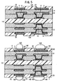
- the multilayer printed wiring board according to the fourth example is manufactured as will be described herebelow with reference to FIGS. 3 and 4.
- the manufacturing process is substantially same as that for the first embodiment and thus includes the previously mentioned steps (1) to (14).
- a composite of fluororesin and heat-resistant thermoplastic resin, composite of fluororesin and thermosetting resin or a composite of thermosetting and thermoplastic resins is used as the interlaminar insulative resin layer.
- an electroless plating adhesive using the composite as resin matrix should preferably be used.
- the hole for the viahole is formed by exposing, developing and then thermally curing the resin layer.
- the resin is a composite of fluororesin and heat-resistant thermoplastic resin, composite of fluororesin and thermosetting resin or a composite of thermosetting and thermoplastic resins
- the hole for the viahole is formed by thermosetting the resin layer and then by lasing drilling.
- the ratio D/T 1 between the viahole diameter (D) and interlaminar insulative resin layer thickness (T 1 ) should preferably be within a range of 1 to 4. This is because if the ratio D/T 1 is less than 1, the electroplating solution will not enter the hole while the ratio over 4 will not allow the hole to sufficiently be filled with a plating metal.
- the surface of the interlaminar insulative resin layer should preferably be roughened by plasma etching or the like for this roughening will improve the adhesion to the plating layer.
- the epoxy resin particles existent on the surface of the cured adhesive layer are removed by decomposing or dissolving with an acid or oxidant to rough the surface of the adhesive layer.
- examples 1 to 9 and comparative examples 1 to 8 of multilayer printed wiring boards were prepared through the steps (1) to (11) of the 14 steps having been described in the foregoing, not yet including the step at which the solder bump is formed.
- Example 11 was prepared through all the steps (1) to (14). Themultilayer printed wiring boards thus prepared will further be described in detail herebelow:
- compositions prepared through the following steps 1 to 3 were mixed together and agitated to prepare an electroless plating adhesive.
- a multilayer printed wiring board was prepared in the same manner as the aforementioned example 1 except that an interlaminar insulative resin layer was formed by attaching a fluororesin film of 20 ⁇ m in thickness to the layer by thermo-compression bonding and holes for viaholes of 60 ⁇ m in diameter were formed by irradiating ultraviolet laser.
- a multilayer printed wiring board was produced in the same manner as the aforementioned example 1 except that a conductor circuit was made only of an electroless plating layer of 25 ⁇ m in thickness and viaholes were formed by dipping for 11 hours in en electroless plating aqueous solution composed of 0.06 mol/l of copper sulfide, 0.3 mol/l of formalin, 0.35 mol/l of NaOH, 0.35 mol/l of EDTA and a small amount of additive at 75°C and having a pH of 12.4.
- the holes in the interlaminar insulative resin layer were found filled with the plating layer, but a depression of 20 to 25 m was found in the central portion of the plating layer.
- a multilayer printed wiring board was produced. More particularly, the steps (1) to (5) for the embodiment 1 were repeated to process a substrate and then the substrate was dipped in an electroless plating solution prepared from an aqueous solution composed of 0.05 mol/l of copper sulfide, 0.30 mol/l of formalin, 0.35 mol/l of sodium hydroxide, and 0.35 mol/l of ethylenediaminetetraacetic acid (EDTA) to form a plating layer of 40 ⁇ m in thickness.
- an electroless plating solution prepared from an aqueous solution composed of 0.05 mol/l of copper sulfide, 0.30 mol/l of formalin, 0.35 mol/l of sodium hydroxide, and 0.35 mol/l of ethylenediaminetetraacetic acid (EDTA) to form a plating layer of 40 ⁇ m in thickness.
- etching resist 25/25 ⁇ m on the substrate.
- the substrate was dipped in a mixed solution of sulfuric acid and hydrogen peroxide.
- the conductor circuitry layer was undercut and separated. Therefore, the comparative example 2 was not evaluated.
- the examples 1 to 3 and comparative example 1 were evaluated as to 1 surface flatness of their interlaminar insulative resin layer and 2 electrical connection reliability of the viahole.
- the above item 1 surface flatness, was evaluated by judging whether a depression developed on a first applied interlaminar insulative resin layer.
- the item 2 electrical connection reliability of the viahole, was evaluated by checking, using a probe, whether a further viahole formed on a viahole already formed showed a poor electrical continuity. The evaluation results are shown in Table 1.
- the examples 1, 2 and 3 are superior in surface flatness of the interlaminar insulative resin layer. Even when the further viahole is provided on the inner one, a circuit pattern breaking due to a depression is not observed, namely, the examples Table 1 Depression on interlaminar insulative resin layer Poor electrical continuity
- Example 1 No No Example 2 - No Example 3 - No Comparative example 1 Yes No 1 to 3 have a high electrical connection reliability of the viahole, and IC chip and other devices can easily be mounted on the wiring boards with no inconvenience. Further, even when mass-produced, the examples 1 to 3 will show a high electrical connection reliability of the viaholes.
- the first embodiment of the present invention provides a multilayer printed wiring board having a filled viahole structure enabling a fine circuit pattern to be formed and showing superior surface flatness and high electrical connection reliability of the viahole.
- Aqueous electroplating solution CuSO 4 ⁇ 5H 2 O 60 g/l Leveling agent (HL by ATOTTECK) 40 ml/l Sulfuric acid 190 g/l Brightening agent (UV by ATOTTECH) 0.5 ml/l Chlorine ion 40 ppm
- Electroplating conditions Bubbling 3.0 liters/min Current density 0.5 A/dm 2 Set current value 0.18 A Plating length of time 100 min (8) The plating resist layer 8 was separated and removed, and then the electroless plating layer 7 under the plating resist layer 8 was dissolved for removal in an etching solution composed of a mixture of sulfuric acid and hydrogen peroxide, sodium persulfate, ammoniumpersulfate, etc.
- a multilayer printed wiring board was produced by repeating the steps (1) to (3) for the example 3, and further processing the substrate as follows:
- a multilayer printed wiring board was produced. More particularly, the steps (1) to (5) for the embodiment 5 were repeated and then the substrate was dipped in an electroless plating solution prepared from an aqueous solution composed of 0.05 mol/l of copper sulfide, 0.30 mol/l of formalin, 0. 35 mol/l of sodium hydroxide, and 0.35 mol/l of ethylenediaminetetraacetic acid (EDTA) to form a plating layer of 40 ⁇ m in thickness.
- an electroless plating solution prepared from an aqueous solution composed of 0.05 mol/l of copper sulfide, 0.30 mol/l of formalin, 0. 35 mol/l of sodium hydroxide, and 0.35 mol/l of ethylenediaminetetraacetic acid (EDTA) to form a plating layer of 40 ⁇ m in thickness.
- EDTA ethylenediaminetetraacetic acid
- the substrate was dipped in a mixed solution of sulfuric acid and hydrogen peroxide.
- the conductor circuitry layer was undercut and separated.
- Aqueous electroplating solution CuSO 4 ⁇ 5H 2 O 60 g/l Leveling agent (HL by ATOTTECH) 40 ml/l Sulfuric acid 190 g/l Brightening agent (UV by ATOTTECH) 0.5 ml/l Chlorine ion 40 ppm
- Electroplating conditions Bubbling 3.0 liters/min Current density 0.5 A/dm 2 Set current value 0.18 A Plating length of time 100 min (8) The plating resist layer 8 was separated and removed, and then the electroless plating layer 7 under the plating resist layer 8 was dissolved for removal in an etching solution composed of a mixture of sulfuric acid and hydrogen peroxide, sodium persulfate, ammoniumpersulfate, etc.
- a multilayer printed wiring board was produced by repeating the steps (1) to (3) for the example 2, and further processing the substrate as follows:
- a multilayer printed wiring board was produced similarly to the embodiment as disclosed in the Japanese unexamined patent publication No. hei 2-188992.
- the holes for viaholes were filled only with the electroless plating layer to form the viaholes.
- a multilayer printed wiring board was produced by repeating the steps (1) to (3) for the example 6 and further processing the substrate as follows.
- the substrate was dipped in an electroless plating solution prepared from an aqueous solution composed of 0.05 mol/l of copper sulfide, 0.30 mol/l of formalin, 0.35 mol/l of sodium hydroxide, and 0.35 mol/l of ethylenediaminetetraacetic acid (EDTA) to form a plating layer of 1 ⁇ m in thickness.
- an electroless plating solution prepared from an aqueous solution composed of 0.05 mol/l of copper sulfide, 0.30 mol/l of formalin, 0.35 mol/l of sodium hydroxide, and 0.35 mol/l of ethylenediaminetetraacetic acid (EDTA) to form a plating layer of 1 ⁇ m in thickness.
- EDTA ethylenediaminetetraacetic acid
- this multilayer printed wiring board had no roughed surface on the viahole.
- the comparative example 5 showed a cracking in the viahole portion
- the comparative example 6 showed a separation of the viahole portion
- the examples 6 and 7 showed neither separation nor cracking at the viahole portion.
- the third embodiment of the present invention provides a multilayer printed wiring board having a filled viahole structure in which the viahole is not easily separable and no crack takes place under a thermal shock or due to heat cycle.
- a multilayer printed wiring board not according to the invention however, was produced of which the interlaminar insulative resin layer was made of a composite of fluororesin and heat-resistant thermoplastic resin, through a process including the following steps: (1) An interlaminar insulative resin liquid was prepared by thermally fusing and mixing eight parts by weight of polyether sulfone (PES) and 92 parts by weight of fluororesin (Teflon by Du Pont) at 350°C. (2) A substrate 1 made of bismaleimide triazine (BT) and having a conductor circuitry layer 2 formed on either surface thereof (as in FIG.
- PES polyether sulfone
- Teflon by Du Pont fluororesin
- a plating resist layer 8 was formed on the electroless plating copper layer 7 in the conventional manner (see FIG. 4(a)). (7) Next, a portion on which the plating resist layer 8 was not formed was electroplated under the following conditions to form an electroplating layer of 15 ⁇ m in thickness on the portion.
- the layer 9 provided a conductor layer on which a conductor circuit was to be formed, and the electroplating layer 9 was filled in the hole to form a viahole 10 (as in FIG. 4(b)).
- Aqueous electroplating solution CuSO 4 ⁇ 5H 2 O 60 g/l Leveling agent (HL by ATOTTECH) 40 ml/l Sulfuric acid 190 g/l Brightening agent (UV by ATOTTECH) 0.5 ml/l Chlorine ion 40 ppm
- Electroplating conditions Bubbling 3.0 liters/min Current density 0.5 A/dm 2 Set current value 0.18 A Plating length of time 130 min (8) The plating resist layer 8 was separated and removed, and then the electroless plating copper layer 7 under the plating resist layer 8 was dissolved for removal in an etching solution composed of a mixture of sulfuric acid and hydrogen peroxide, sodium persulfate, ammoniumpersulfate, etc.
- the viahole 10 had a flat surface, and the conductor circuitry layer surface was at a same level as the viahole surface.
- a rough surface layer 3 was formed on the substrate. Further, the steps (3) to (8) were repeated to produce the multilayer printed wiring board (as in FIG. 4(c)).
- a multilayer printed wiring board was produced of which the interlaminar insulative resin layer was made of a composite of fluororesin and thermosetting resin, by repeating the above steps (1) to (3) for the example 3 and further processing the substrate as follows:
- a multilayer printed wiring board of which the interlaminar insulative resin layer was made of a composite of thermosetting and thermoplastic resins was produced by repeating the steps (1) to (6) for the example 1 and further processing the substrate as follows:
- the viahole 10 had a flat surface, and the conductor surface was at a same level as the viahole surface.
- a multilayer printed wiring board was produced of which the interlaminar insulative resin layer was made only of a thermosetting resin, as follows:
- steps (2) to (9) for the example 10 were repeated to provide the multilayer printed wiring board.
- a multilayer printed wiring board was produced in the same manner as for the example 8 except that no leveling agent and brightening agent were added to the electroplating solution. As a result, a plating layer could not sufficiently be filled in the holes for the viaholes.
- the example 8 is highly resistant against violent temperature variation since its interlaminar insulative resin layer incorporates a fluororesin and thermoplastic resin.
- the fourth embodiment of the present invention provides a multilayer printed wiring board having a filled viahole structure permitting to positively prevent line breakage in the wiring board and improved in resistance against violent temperature variation.
- a multilayer printed wiring board was produced by repeating the steps (1) to (9) for the example 1, and further processing the substrate as follows:
- a solder resist composition was prepared by mixing 46.67 parts by weight of a photosensitive oligomer (4000 in molecular weight) produced by acrylating 50% of epoxy group of a 60% by weight of cresol novolac type epoxy resin (by Nippon Kayaku Co., Ltd.)solved in DMDG (diethyleneglycoldimethylether), 6.666 parts by weight of a 80% by weight of bisphenol A type epoxy resin (EPICOAT 1001 by YUKA SHELL) solved in MEK (methyletylketone), 6.666 parts by weight of an epoxy resin of the same bisphenol A type (EPICOAT E-1001-B80 by YUKA SHELL), 1.6 parts by weight of imidazole (2E4MZ-CN by Shikoku Kasei Co.
- a polyvalent acryl monomer being a photosensitive monomer R604 by Nippon Kayaku Co., Ltd.
- a same polyfunctional acryl monomer DPE6A by KYOEISHA KAGAKU Co., Ltd.
- leveling agent made from an acrylic ester polymer POLYFLOW No. 75 by KYOEISHA KAGAKU.
- 2.0 parts by weight of an initiator IRGACURE I-907 by Ciba Geigy
- 0.2 part by weight of photosensitizer DETX-S (by Nippon Kayaku Co., Ltd.) were added to the above mixture.
- 0.6 part by weight of DMDG was added to the mixture to adjust the viscosity to 1.4 ⁇ 0.3 Pa ⁇ s at 25°C.
- the viscosity of the solder resist composition was measured using a B-type viscometer (DVL-B by Tokyo Keiki). For 60 rpm, No. 4 rotor was used with the viscometer. For 6 rpm, No. 3 rotor was used.
- the present invention provides a multilayer printed wiring board best suitable for forming a fine circuit pattern thereon, providing an excellent adhesion between the conductor circuit and interlaminar insulative resin layer and an outstanding resistance against cracking due to heat cycle.
- the multilayer printed wiring board according to the present invention has an excellent applicability in many fields of art requiring a high performance and high packaging density of electronic parts.
Landscapes
- Engineering & Computer Science (AREA)
- Manufacturing & Machinery (AREA)
- Microelectronics & Electronic Packaging (AREA)
- Production Of Multi-Layered Print Wiring Board (AREA)
- Manufacturing Of Printed Wiring (AREA)
- Printing Elements For Providing Electric Connections Between Printed Circuits (AREA)
Claims (6)
- Mehrschichtige Leiterplatte mit Leiter-Schaltungsschichten (2, 12) und isolierenden Harz-Zwischenschichten (4), die abwechselnd aufeinander abgeschieden sind, wobei durch die isolierenden Harz-Zwischenschichten (4) hindurch jeweils Löcher (5) ausgebildet sind, die gefüllt sind, um ein gefülltes Kontaktloch (10) auszubilden, unddie Innenwand des Lochs (5) aufgeraut ist;die Oberflächen der inneren Leiter-Schaltung (2), die über das Kontaktloch miteinander verbunden sind, aufgeraut sind;die aufgeraute Innenwand und die aufgeraute Oberfläche (3) mit einer stromlos abgeschiedenen Schicht (7) bedeckt sind,
dadurch gekennzeichnet, dassdie stromlos abgeschiedene Schicht (7) aufgeraut ist und ein Innenraum der Löcher, der durch die stromlos abgeschiedene Schicht (7) begrenzt ist, mit einer durch Elektroplattieren abgeschiedenen Schicht (9) gefüllt ist. - Mehrschichtige Leiterplatte nach Anspruch 1, wobei die Oberfläche der abgeschiedenen Schicht (9) sowie die Oberfläche der Leiter-Schaltung (12), die über das Loch für das Kontaktloch (10) freiliegt, aufgeraut sind.
- Mehrschichtige Leiterplatte nach einem der Ansprüche 1 oder 2, wobei ein weiteres Kontaktloch (20) an dem Kontaktloch (10) ausgebildet ist.
- Mehrschichtige Leiterplatte nach einem der Ansprüche 1 bis 3, wobei die isolierende Harz-Zwischenschicht (4), in der das Kontaktloch (10) ausgebildet ist, aus einem Thermoplastharz oder einem Verbundstoff aus Thermoplastharz und wärmehärtbarem Harz besteht.
- Mehrschichtige Leiterplatte nach einem der Ansprüche 1 bis 4, wobei das Verhältnis zwischen dem Durchmesser (D) des Kontaktlochs und der Dicke (4, T1) der isolierenden Harz-Zwischenschicht innerhalb eines Bereiches von 1 bis 4 liegt.
- Mehrschichtige Leiterplatte nach einem der Ansprüche 1 bis 5, wobei die Dicke (T2) der Leiter-Schaltungsschicht (1, 12) geringer ist als 25 µm.
Priority Applications (1)
| Application Number | Priority Date | Filing Date | Title |
|---|---|---|---|
| EP20070008979 EP1811825A1 (de) | 1998-02-26 | 1999-02-05 | Mehrschichtige Leiterplatte mit gefüllten Kontaktlöchern |
Applications Claiming Priority (9)
| Application Number | Priority Date | Filing Date | Title |
|---|---|---|---|
| JP4539898 | 1998-02-26 | ||
| JP10045397A JPH11243277A (ja) | 1998-02-26 | 1998-02-26 | フィルドビア構造を有する多層プリント配線板 |
| JP10045398A JPH11243278A (ja) | 1998-02-26 | 1998-02-26 | フィルドビア構造を有する多層プリント配線板 |
| JP4539998 | 1998-02-26 | ||
| JP10045396A JPH11243280A (ja) | 1998-02-26 | 1998-02-26 | フィルドビア構造を有する多層プリント配線板 |
| JP4539698 | 1998-02-26 | ||
| JP4539798 | 1998-02-26 | ||
| JP10045399A JPH11243279A (ja) | 1998-02-26 | 1998-02-26 | フィルドビア構造を有する多層プリント配線板 |
| EP19990902842 EP1075172B1 (de) | 1998-02-26 | 1999-02-05 | Mehrschichtige leiterplatte mit einer struktur von gefüllten kontaktlöchern |
Related Parent Applications (1)
| Application Number | Title | Priority Date | Filing Date |
|---|---|---|---|
| EP19990902842 Division EP1075172B1 (de) | 1998-02-26 | 1999-02-05 | Mehrschichtige leiterplatte mit einer struktur von gefüllten kontaktlöchern |
Related Child Applications (1)
| Application Number | Title | Priority Date | Filing Date |
|---|---|---|---|
| EP20070008979 Division EP1811825A1 (de) | 1998-02-26 | 1999-02-05 | Mehrschichtige Leiterplatte mit gefüllten Kontaktlöchern |
Publications (2)
| Publication Number | Publication Date |
|---|---|
| EP1583407A1 EP1583407A1 (de) | 2005-10-05 |
| EP1583407B1 true EP1583407B1 (de) | 2007-05-30 |
Family
ID=27461693
Family Applications (4)
| Application Number | Title | Priority Date | Filing Date |
|---|---|---|---|
| EP20040024664 Expired - Lifetime EP1505859B1 (de) | 1998-02-26 | 1999-02-05 | Mehrschichtige Leiterplatte mit gefüllten Kontaktlöchern |
| EP20070008979 Withdrawn EP1811825A1 (de) | 1998-02-26 | 1999-02-05 | Mehrschichtige Leiterplatte mit gefüllten Kontaktlöchern |
| EP20050012908 Expired - Lifetime EP1583407B1 (de) | 1998-02-26 | 1999-02-05 | Mehrschichtige Leiterplatte mit gefüllten Kontaktlöchern |
| EP19990902842 Expired - Lifetime EP1075172B1 (de) | 1998-02-26 | 1999-02-05 | Mehrschichtige leiterplatte mit einer struktur von gefüllten kontaktlöchern |
Family Applications Before (2)
| Application Number | Title | Priority Date | Filing Date |
|---|---|---|---|
| EP20040024664 Expired - Lifetime EP1505859B1 (de) | 1998-02-26 | 1999-02-05 | Mehrschichtige Leiterplatte mit gefüllten Kontaktlöchern |
| EP20070008979 Withdrawn EP1811825A1 (de) | 1998-02-26 | 1999-02-05 | Mehrschichtige Leiterplatte mit gefüllten Kontaktlöchern |
Family Applications After (1)
| Application Number | Title | Priority Date | Filing Date |
|---|---|---|---|
| EP19990902842 Expired - Lifetime EP1075172B1 (de) | 1998-02-26 | 1999-02-05 | Mehrschichtige leiterplatte mit einer struktur von gefüllten kontaktlöchern |
Country Status (8)
| Country | Link |
|---|---|
| US (6) | US7071424B1 (de) |
| EP (4) | EP1505859B1 (de) |
| KR (4) | KR100906931B1 (de) |
| CN (2) | CN100475005C (de) |
| DE (3) | DE69928518T2 (de) |
| MY (1) | MY129801A (de) |
| TW (1) | TW404158B (de) |
| WO (1) | WO1999044403A1 (de) |
Families Citing this family (128)
| Publication number | Priority date | Publication date | Assignee | Title |
|---|---|---|---|---|
| KR100906931B1 (ko) * | 1998-02-26 | 2009-07-10 | 이비덴 가부시키가이샤 | 필드 바이어 구조를 갖는 다층프린트 배선판 |
| EP1744609B1 (de) | 1999-06-02 | 2012-12-12 | Ibiden Co., Ltd. | Gedruckte mehrlagige Schaltungsplatte und Verfahren zur Herstellung |
| WO2001011932A1 (en) | 1999-08-06 | 2001-02-15 | Ibiden Co., Ltd. | Electroplating solution, method for fabricating multilayer printed wiring board using the solution, and multilayer printed wiring board |
| JP4062907B2 (ja) * | 2001-11-12 | 2008-03-19 | 松下電器産業株式会社 | 回路基板およびその製造方法 |
| JP4029759B2 (ja) * | 2003-04-04 | 2008-01-09 | 株式会社デンソー | 多層回路基板およびその製造方法 |
| TW200521171A (en) | 2003-12-26 | 2005-07-01 | Toshiba Kk | Resin particles and resin layer containing metal micro particles, its forming method and circuit base board |
| JP4426900B2 (ja) * | 2004-05-10 | 2010-03-03 | 三井金属鉱業株式会社 | プリント配線基板、その製造方法および半導体装置 |
| US7626829B2 (en) | 2004-10-27 | 2009-12-01 | Ibiden Co., Ltd. | Multilayer printed wiring board and manufacturing method of the multilayer printed wiring board |
| KR100845534B1 (ko) * | 2004-12-31 | 2008-07-10 | 엘지전자 주식회사 | 전도성 금속 도금 폴리이미드 기판 및 그 제조 방법 |
| CN100423254C (zh) * | 2005-02-14 | 2008-10-01 | 富士通株式会社 | 半导体器件及其制造方法与电容器结构及其制造方法 |
| KR100688864B1 (ko) * | 2005-02-25 | 2007-03-02 | 삼성전기주식회사 | 인쇄회로기판, 플립칩 볼 그리드 어레이 기판 및 그 제조방법 |
| TWI261329B (en) | 2005-03-09 | 2006-09-01 | Phoenix Prec Technology Corp | Conductive bump structure of circuit board and method for fabricating the same |
| US7701071B2 (en) * | 2005-03-24 | 2010-04-20 | Texas Instruments Incorporated | Method for fabricating flip-attached and underfilled semiconductor devices |
| JP4790297B2 (ja) * | 2005-04-06 | 2011-10-12 | ルネサスエレクトロニクス株式会社 | 半導体装置およびその製造方法 |
| US7650694B2 (en) * | 2005-06-30 | 2010-01-26 | Intel Corporation | Method for forming multilayer substrate |
| JP2007042666A (ja) * | 2005-07-29 | 2007-02-15 | Victor Co Of Japan Ltd | プリント配線板及びその製造方法 |
| KR101266564B1 (ko) * | 2005-08-03 | 2013-05-22 | 제이에스알 가부시끼가이샤 | 도금 조형물 제조용 포지티브형 감방사선성 수지 조성물,전사 필름 및 도금 조형물의 제조 방법 |
| IL171378A (en) * | 2005-10-11 | 2010-11-30 | Dror Hurwitz | Integrated circuit support structures and the fabrication thereof |
| US7416923B2 (en) * | 2005-12-09 | 2008-08-26 | International Business Machines Corporation | Underfill film having thermally conductive sheet |
| JP2007173371A (ja) * | 2005-12-20 | 2007-07-05 | Shinko Electric Ind Co Ltd | フレキシブル配線基板の製造方法及び電子部品実装構造体の製造方法 |
| US7906850B2 (en) * | 2005-12-20 | 2011-03-15 | Unimicron Technology Corp. | Structure of circuit board and method for fabricating same |
| DE102006028692B4 (de) * | 2006-05-19 | 2021-09-02 | OSRAM Opto Semiconductors Gesellschaft mit beschränkter Haftung | Elektrisch leitende Verbindung mit isolierendem Verbindungsmedium |
| KR100797692B1 (ko) | 2006-06-20 | 2008-01-23 | 삼성전기주식회사 | 인쇄회로기판 및 그 제조방법 |
| US7570082B2 (en) * | 2006-08-15 | 2009-08-04 | International Business Machines Corporation | Voltage comparator apparatus and method having improved kickback and jitter characteristics |
| WO2008053833A1 (fr) * | 2006-11-03 | 2008-05-08 | Ibiden Co., Ltd. | Tableau de câblage imprimé multicouche |
| JP5214139B2 (ja) * | 2006-12-04 | 2013-06-19 | 新光電気工業株式会社 | 配線基板及びその製造方法 |
| CN101296570A (zh) * | 2007-04-25 | 2008-10-29 | 富葵精密组件(深圳)有限公司 | 电路板及其制作方法 |
| US7969005B2 (en) * | 2007-04-27 | 2011-06-28 | Sanyo Electric Co., Ltd. | Packaging board, rewiring, roughened conductor for semiconductor module of a portable device, and manufacturing method therefor |
| JP2009010276A (ja) * | 2007-06-29 | 2009-01-15 | C Uyemura & Co Ltd | 配線基板の製造方法 |
| KR100811620B1 (ko) | 2007-07-02 | 2008-03-07 | 에스티주식회사 | 인쇄회로기판의 제조방법 |
| US8192815B2 (en) | 2007-07-13 | 2012-06-05 | Apple Inc. | Methods and systems for forming a dual layer housing |
| TWI358981B (en) * | 2007-08-08 | 2012-02-21 | Unimicron Technology Corp | Method for fabricating circuit board |
| CN101409982B (zh) * | 2007-10-09 | 2010-06-16 | 南亚电路板股份有限公司 | 电路板的制造方法 |
| JP2009099589A (ja) * | 2007-10-12 | 2009-05-07 | Elpida Memory Inc | ウエハまたは回路基板およびその接続構造体 |
| USPP19906P2 (en) * | 2007-10-31 | 2009-04-14 | Tai-Ling Biotech Inc. | Phalaenopsis plant named ‘Queen V6’ |
| US8309856B2 (en) * | 2007-11-06 | 2012-11-13 | Ibiden Co., Ltd. | Circuit board and manufacturing method thereof |
| KR101514726B1 (ko) * | 2007-11-22 | 2015-04-23 | 아지노모토 가부시키가이샤 | 다층 인쇄 배선 기판의 제조 방법 및 다층 인쇄 배선 기판 |
| KR20090067249A (ko) * | 2007-12-21 | 2009-06-25 | 삼성전기주식회사 | 인쇄회로기판 및 그 제조방법 |
| US8315043B2 (en) * | 2008-01-24 | 2012-11-20 | Apple Inc. | Methods and systems for forming housings from multi-layer materials |
| JP2009182272A (ja) * | 2008-01-31 | 2009-08-13 | Sanyo Electric Co Ltd | 素子搭載用基板およびその製造方法、半導体モジュールおよびその製造方法、ならびに携帯機器 |
| JP2009231596A (ja) * | 2008-03-24 | 2009-10-08 | Fujitsu Ltd | 多層配線板、多層配線板ユニット、および電子機器 |
| US8646637B2 (en) * | 2008-04-18 | 2014-02-11 | Apple Inc. | Perforated substrates for forming housings |
| US8367304B2 (en) * | 2008-06-08 | 2013-02-05 | Apple Inc. | Techniques for marking product housings |
| KR100962369B1 (ko) * | 2008-06-26 | 2010-06-10 | 삼성전기주식회사 | 인쇄회로기판 및 그 제조방법 |
| KR100999918B1 (ko) * | 2008-09-08 | 2010-12-13 | 삼성전기주식회사 | 인쇄회로기판 및 그 제조 방법 |
| JP5203108B2 (ja) | 2008-09-12 | 2013-06-05 | 新光電気工業株式会社 | 配線基板及びその製造方法 |
| CN102573268B (zh) * | 2008-09-30 | 2015-03-11 | 揖斐电株式会社 | 多层印刷线路板以及多层印刷线路板的制造方法 |
| US20100159273A1 (en) | 2008-12-24 | 2010-06-24 | John Benjamin Filson | Method and Apparatus for Forming a Layered Metal Structure with an Anodized Surface |
| FR2940879B1 (fr) * | 2009-01-06 | 2012-12-21 | Thales Sa | Procede de realisation d'une carte imprimee et carte imprimee correspondante |
| CN101790288B (zh) * | 2009-01-22 | 2012-08-29 | 上海美维科技有限公司 | 一种印制电路板的制造方法 |
| US9884342B2 (en) | 2009-05-19 | 2018-02-06 | Apple Inc. | Techniques for marking product housings |
| US9173336B2 (en) | 2009-05-19 | 2015-10-27 | Apple Inc. | Techniques for marking product housings |
| US9627254B2 (en) * | 2009-07-02 | 2017-04-18 | Flipchip International, Llc | Method for building vertical pillar interconnect |
| US8426959B2 (en) * | 2009-08-19 | 2013-04-23 | Samsung Electronics Co., Ltd. | Semiconductor package and method of manufacturing the same |
| US8663806B2 (en) | 2009-08-25 | 2014-03-04 | Apple Inc. | Techniques for marking a substrate using a physical vapor deposition material |
| JP5561279B2 (ja) * | 2009-09-02 | 2014-07-30 | パナソニック株式会社 | プリント配線板、ビルドアップ多層基板とその製造方法 |
| US9845546B2 (en) | 2009-10-16 | 2017-12-19 | Apple Inc. | Sub-surface marking of product housings |
| US8809733B2 (en) | 2009-10-16 | 2014-08-19 | Apple Inc. | Sub-surface marking of product housings |
| US10071583B2 (en) | 2009-10-16 | 2018-09-11 | Apple Inc. | Marking of product housings |
| US8067266B2 (en) * | 2009-12-23 | 2011-11-29 | Intel Corporation | Methods for the fabrication of microelectronic device substrates by attaching two cores together during fabrication |
| CN102118925A (zh) * | 2009-12-30 | 2011-07-06 | 深圳富泰宏精密工业有限公司 | 电子装置外壳及其制作方法 |
| JP5603600B2 (ja) * | 2010-01-13 | 2014-10-08 | 新光電気工業株式会社 | 配線基板及びその製造方法、並びに半導体パッケージ |
| US8628836B2 (en) * | 2010-03-02 | 2014-01-14 | Apple Inc. | Method and apparatus for bonding metals and composites |
| TW201132246A (en) * | 2010-03-09 | 2011-09-16 | Nan Ya Printed Circuit Board | Side packaged type printed circuit board |
| JP5638269B2 (ja) * | 2010-03-26 | 2014-12-10 | 日本特殊陶業株式会社 | 多層配線基板 |
| US8489158B2 (en) | 2010-04-19 | 2013-07-16 | Apple Inc. | Techniques for marking translucent product housings |
| TWI381780B (zh) * | 2010-04-28 | 2013-01-01 | Wus Printed Circuit Co Ltd | 可辨識印刷電路板之製造方法 |
| US8724285B2 (en) | 2010-09-30 | 2014-05-13 | Apple Inc. | Cosmetic conductive laser etching |
| US8901431B2 (en) * | 2010-12-16 | 2014-12-02 | Ibiden Co., Ltd. | Printed wiring board and method for manufacturing printed wiring board |
| US8569861B2 (en) * | 2010-12-22 | 2013-10-29 | Analog Devices, Inc. | Vertically integrated systems |
| JP2012182437A (ja) * | 2011-02-09 | 2012-09-20 | Ngk Spark Plug Co Ltd | 配線基板及びその製造方法 |
| JP5675443B2 (ja) * | 2011-03-04 | 2015-02-25 | 新光電気工業株式会社 | 配線基板及び配線基板の製造方法 |
| US20120248001A1 (en) | 2011-03-29 | 2012-10-04 | Nashner Michael S | Marking of Fabric Carrying Case for Portable Electronic Device |
| US9280183B2 (en) | 2011-04-01 | 2016-03-08 | Apple Inc. | Advanced techniques for bonding metal to plastic |
| DE102011006899B4 (de) * | 2011-04-06 | 2025-01-30 | Te Connectivity Germany Gmbh | Verfahren zur Herstellung von Kontaktelementen durch mechanisches Aufbringen von Materialschicht mit hoher Auflösung sowie Kontaktelement und eine Vorrichtung zur Herstellung |
| US20120286416A1 (en) * | 2011-05-11 | 2012-11-15 | Tessera Research Llc | Semiconductor chip package assembly and method for making same |
| US8879266B2 (en) * | 2012-05-24 | 2014-11-04 | Apple Inc. | Thin multi-layered structures providing rigidity and conductivity |
| US10071584B2 (en) | 2012-07-09 | 2018-09-11 | Apple Inc. | Process for creating sub-surface marking on plastic parts |
| KR101506785B1 (ko) * | 2013-05-29 | 2015-03-27 | 삼성전기주식회사 | 인쇄회로기판 |
| US9434197B2 (en) | 2013-06-18 | 2016-09-06 | Apple Inc. | Laser engraved reflective surface structures |
| US9314871B2 (en) | 2013-06-18 | 2016-04-19 | Apple Inc. | Method for laser engraved reflective surface structures |
| CA2917884A1 (en) | 2013-07-09 | 2015-01-15 | United Technologies Corporation | Plated polymer fan |
| US10927843B2 (en) | 2013-07-09 | 2021-02-23 | Raytheon Technologies Corporation | Plated polymer compressor |
| WO2015006421A1 (en) | 2013-07-09 | 2015-01-15 | United Technologies Corporation | Metal-encapsulated polymeric article |
| WO2015017095A2 (en) | 2013-07-09 | 2015-02-05 | United Technologies Corporation | Plated polymer nosecone |
| KR101483875B1 (ko) * | 2013-07-31 | 2015-01-16 | 삼성전기주식회사 | 글라스 코어기판 및 그 제조방법 |
| TWM470379U (zh) * | 2013-09-05 | 2014-01-11 | 思鷺科技股份有限公司 | 陶瓷電路板及具有該陶瓷電路板的led封裝模組 |
| CN103732011B (zh) * | 2013-12-24 | 2016-06-08 | 广州兴森快捷电路科技有限公司 | 印制线路板盲孔的制作方法 |
| US9398703B2 (en) * | 2014-05-19 | 2016-07-19 | Sierra Circuits, Inc. | Via in a printed circuit board |
| JP2015222753A (ja) * | 2014-05-22 | 2015-12-10 | イビデン株式会社 | プリント配線板及びその製造方法 |
| KR102412612B1 (ko) * | 2015-08-28 | 2022-06-23 | 삼성전자주식회사 | 패키지 기판 및 프리프레그 |
| US20170064821A1 (en) * | 2015-08-31 | 2017-03-02 | Kristof Darmawikarta | Electronic package and method forming an electrical package |
| KR20170038535A (ko) * | 2015-09-30 | 2017-04-07 | 삼성전기주식회사 | 인쇄회로기판 및 그 제조방법 |
| KR102546379B1 (ko) * | 2015-10-22 | 2023-06-21 | 에이지씨 가부시키가이샤 | 배선 기판의 제조 방법 |
| TWI574595B (zh) | 2015-10-28 | 2017-03-11 | 財團法人工業技術研究院 | 多層線路的製作方法與多層線路結構 |
| US9633924B1 (en) * | 2015-12-16 | 2017-04-25 | Taiwan Semiconductor Manufacturing Company, Ltd. | Package structure and method for forming the same |
| US10177131B2 (en) | 2016-03-02 | 2019-01-08 | Samsung Electronics Co., Ltd. | Semiconductor packages and methods of manufacturing the same |
| JP2017191894A (ja) * | 2016-04-14 | 2017-10-19 | イビデン株式会社 | プリント配線基板及びその製造方法 |
| JP2017199803A (ja) * | 2016-04-27 | 2017-11-02 | 日立マクセル株式会社 | 三次元成形回路部品 |
| WO2017212742A1 (ja) | 2016-06-09 | 2017-12-14 | 株式会社村田製作所 | 弾性波装置 |
| JPWO2018043682A1 (ja) * | 2016-09-01 | 2019-06-24 | Agc株式会社 | 配線基板およびその製造方法 |
| CN106535506A (zh) * | 2016-12-15 | 2017-03-22 | 泰和电路科技(惠州)有限公司 | 过电孔的填孔方法、焊盘的制作方法、焊盘及线路板 |
| US10163847B2 (en) * | 2017-03-03 | 2018-12-25 | Tdk Corporation | Method for producing semiconductor package |
| JP6894289B2 (ja) * | 2017-05-17 | 2021-06-30 | 新光電気工業株式会社 | 配線基板及びその製造方法 |
| WO2019005116A1 (en) * | 2017-06-30 | 2019-01-03 | Manepalli Rahul N | SEMICONDUCTOR HOUSING AND METHOD OF MANUFACTURING |
| TWI658767B (zh) | 2017-09-28 | 2019-05-01 | Unimicron Technology Corp. | 電路板的製造方法以及應用於製造其之堆疊結構 |
| CN109600928B (zh) * | 2017-09-30 | 2021-04-02 | 欣兴电子股份有限公司 | 电路板的制造方法以及应用于制造其的堆叠结构 |
| US10827624B2 (en) * | 2018-03-05 | 2020-11-03 | Catlam, Llc | Catalytic laminate with conductive traces formed during lamination |
| KR20190130749A (ko) | 2018-05-15 | 2019-11-25 | 정지성 | 영업용 운동용품 건조기 및 이를 이용한 건조방법 |
| US10506712B1 (en) * | 2018-07-31 | 2019-12-10 | Taiwan Semiconductor Manufacturing Co., Ltd. | Printed circuit board |
| US10999917B2 (en) | 2018-09-20 | 2021-05-04 | Apple Inc. | Sparse laser etch anodized surface for cosmetic grounding |
| WO2020065938A1 (ja) * | 2018-09-28 | 2020-04-02 | シャープ株式会社 | 表示デバイス |
| KR102124324B1 (ko) * | 2018-11-14 | 2020-06-18 | 와이엠티 주식회사 | 도금 적층체 및 인쇄회로기판 |
| KR102724892B1 (ko) | 2018-12-04 | 2024-11-01 | 삼성전기주식회사 | 인쇄회로기판 및 그 제조방법 |
| US11039540B2 (en) * | 2019-01-01 | 2021-06-15 | Catlam, Llc | Multi-layer circuit board with traces thicker than a circuit board layer |
| TWI706705B (zh) * | 2019-06-21 | 2020-10-01 | 唐虞企業股份有限公司 | 電路板及其製造方法 |
| KR102762871B1 (ko) * | 2019-11-27 | 2025-02-07 | 삼성전기주식회사 | 인쇄회로기판 |
| WO2021200538A1 (ja) * | 2020-03-30 | 2021-10-07 | 京セラ株式会社 | 印刷配線板及び印刷配線板の製造方法 |
| US11824031B2 (en) * | 2020-06-10 | 2023-11-21 | Advanced Semiconductor Engineering, Inc. | Semiconductor package structure with dielectric structure covering upper surface of chip |
| US11996357B2 (en) * | 2020-09-09 | 2024-05-28 | Ibiden Co., Ltd. | Wiring substrate and method for manufacturing wiring substrate |
| KR20220039071A (ko) * | 2020-09-21 | 2022-03-29 | 삼성전기주식회사 | 전자소자 모듈 및 이에 이용되는 인쇄회로기판 |
| EP4221473A4 (de) * | 2020-09-28 | 2024-11-13 | Kyocera Corporation | Leiterplatte |
| CN113141703A (zh) * | 2021-05-28 | 2021-07-20 | 四会富仕电子科技股份有限公司 | 一种金属基软硬结合板及其生产方法 |
| US11991837B2 (en) * | 2021-06-22 | 2024-05-21 | Unimicron Technology Corp. | Circuit board and manufacturing method thereof |
| JP7768696B2 (ja) * | 2021-07-21 | 2025-11-12 | マクセル株式会社 | 装飾メッキ品 |
| TW202318568A (zh) * | 2021-07-30 | 2023-05-01 | 日商尼康股份有限公司 | 金屬配線的製造方法、電晶體的製造方法及金屬配線 |
| US12324114B2 (en) | 2021-09-24 | 2025-06-03 | Apple Inc. | Laser-marked electronic device housings |
| CN114293056B (zh) * | 2021-12-20 | 2022-12-23 | 富联裕展科技(深圳)有限公司 | 金属工件、金属制品、蚀刻液以及金属工件的制作方法 |
Family Cites Families (86)
| Publication number | Priority date | Publication date | Assignee | Title |
|---|---|---|---|---|
| US3350498A (en) * | 1965-01-04 | 1967-10-31 | Intellux Inc | Multilayer circuit and method of making the same |
| US3536546A (en) | 1968-10-07 | 1970-10-27 | North American Rockwell | Method of improving adhesion of copperepoxy glass laminates |
| JPS5516394B2 (de) * | 1973-01-11 | 1980-05-01 | ||
| JPS56100497A (en) | 1980-01-11 | 1981-08-12 | Mitsumi Electric Co Ltd | Ceramic circuit board |
| JPS5851436B2 (ja) * | 1980-02-29 | 1983-11-16 | 株式会社東芝 | プリント回路板の製造方法 |
| US4747897A (en) * | 1985-02-26 | 1988-05-31 | W. L. Gore & Associates, Inc. | Dielectric materials |
| US4680220A (en) | 1985-02-26 | 1987-07-14 | W. L. Gore & Associates, Inc. | Dielectric materials |
| US4715894A (en) | 1985-08-29 | 1987-12-29 | Techno Instruments Investments 1983 Ltd. | Use of immersion tin and tin alloys as a bonding medium for multilayer circuits |
| JPS62251136A (ja) * | 1986-04-25 | 1987-10-31 | 三菱樹脂株式会社 | 金属複合積層板 |
| JPS62256496A (ja) | 1986-04-30 | 1987-11-09 | 株式会社日立製作所 | 多層配線基板の製造方法 |
| JPH07105577B2 (ja) | 1986-06-02 | 1995-11-13 | ジヤパンゴアテツクス株式会社 | プリント配線基板の製造法 |
| US4937132A (en) | 1987-12-23 | 1990-06-26 | Mitsubishi Gas Chemical Company, Inc. | Laminating material for printed circuit board of low dielectric constant |
| JPH0632386B2 (ja) | 1988-01-19 | 1994-04-27 | イビデン株式会社 | 多層プリント配線板及びその製造方法 |
| DE3913966B4 (de) * | 1988-04-28 | 2005-06-02 | Ibiden Co., Ltd., Ogaki | Klebstoffdispersion zum stromlosen Plattieren, sowie Verwendung zur Herstellung einer gedruckten Schaltung |
| JPH0254599A (ja) | 1988-08-18 | 1990-02-23 | Fujitsu Ltd | 多層プリント基板の製造方法 |
| MY104191A (en) | 1988-09-06 | 1994-02-28 | Mitsubishi Gas Chemical Co | Process for producing multilayer printed wiring board |
| JPH0734505B2 (ja) | 1989-01-18 | 1995-04-12 | イビデン株式会社 | 多層プリント配線板およびその製造方法 |
| JP2776886B2 (ja) * | 1989-05-31 | 1998-07-16 | イビデン株式会社 | 多層プリント配線板およびその製造方法 |
| JP3069356B2 (ja) | 1989-05-31 | 2000-07-24 | イビデン株式会社 | 多層プリント配線板およびその製造方法 |
| JPH06101627B2 (ja) | 1989-10-04 | 1994-12-12 | 日本電気株式会社 | 多層プリント配線板及びその製造方法 |
| JP2688446B2 (ja) * | 1990-03-26 | 1997-12-10 | 株式会社日立製作所 | 多層配線基板およびその製造方法 |
| JP2621634B2 (ja) | 1990-10-24 | 1997-06-18 | 日本電気株式会社 | ポリイミド樹脂多層配線基板の製造方法 |
| US5103293A (en) | 1990-12-07 | 1992-04-07 | International Business Machines Corporation | Electronic circuit packages with tear resistant organic cores |
| JPH053388A (ja) | 1991-06-25 | 1993-01-08 | Fujitsu Ltd | 多層プリント基板の製造方法及び多層プリント基板用絶縁層 |
| JPH0590761A (ja) * | 1991-09-25 | 1993-04-09 | Hitachi Ltd | 配線基板の製造方法 |
| JPH05218645A (ja) | 1992-02-05 | 1993-08-27 | Ngk Insulators Ltd | 薄膜多層配線基板の製造方法 |
| JPH05218646A (ja) | 1992-02-05 | 1993-08-27 | Ngk Insulators Ltd | 薄膜多層配線基板の製造方法 |
| JP3204545B2 (ja) | 1992-08-20 | 2001-09-04 | イビデン株式会社 | 多層プリント配線板およびその製造方法 |
| JPH06196856A (ja) | 1992-09-29 | 1994-07-15 | Matsushita Electric Ind Co Ltd | めっき方法及びその方法を用いた多層プリント配線板の製造方法並びに多層プリント配線板 |
| US5406034A (en) * | 1992-12-21 | 1995-04-11 | Motorola, Inc. | Circuit board having stepped vias |
| JPH06244556A (ja) | 1993-02-19 | 1994-09-02 | Mitsubishi Gas Chem Co Inc | 多層プリント配線板の製造法 |
| JP2790956B2 (ja) | 1993-03-03 | 1998-08-27 | 株式会社日立製作所 | 多層配線板の製法 |
| US5600103A (en) * | 1993-04-16 | 1997-02-04 | Kabushiki Kaisha Toshiba | Circuit devices and fabrication method of the same |
| JPH06310856A (ja) | 1993-04-26 | 1994-11-04 | Hitachi Kasei Ceramics Kk | 多層配線板の製造法 |
| JP3290529B2 (ja) | 1993-05-19 | 2002-06-10 | イビデン株式会社 | 無電解めっき用接着剤、無電解めっき用接着剤層およびプリント配線板 |
| EP0629867B1 (de) * | 1993-06-16 | 1999-01-27 | Nitto Denko Corporation | Sondenkonstruktion |
| JPH0745948A (ja) | 1993-07-28 | 1995-02-14 | Ibiden Co Ltd | 多層配線板及びその製造方法 |
| JPH0779078A (ja) | 1993-09-08 | 1995-03-20 | Shinko Electric Ind Co Ltd | 多層配線基板及びその製造方法 |
| JPH07147483A (ja) | 1993-09-30 | 1995-06-06 | Ibiden Co Ltd | プリント配線板及びその製造方法 |
| JP3527766B2 (ja) | 1993-11-30 | 2004-05-17 | 京セラ株式会社 | 積層回路基板の製造方法及び積層回路基板 |
| JP2694802B2 (ja) * | 1993-12-28 | 1997-12-24 | 日本電気株式会社 | プリント配線板の製造方法 |
| JPH07235768A (ja) | 1994-02-25 | 1995-09-05 | Toshiba Corp | 薄膜多層配線基板の製造方法 |
| JP3602565B2 (ja) | 1994-03-04 | 2004-12-15 | イビデン株式会社 | Icチップを搭載した多層プリント配線板及びそのための多層プリント配線板の製造方法 |
| JPH07283538A (ja) | 1994-04-14 | 1995-10-27 | Ibiden Co Ltd | 多層プリント配線板の製造方法 |
| JPH07283539A (ja) | 1994-04-14 | 1995-10-27 | Sony Corp | ビルドアップ多層プリント配線板 |
| JPH07336017A (ja) | 1994-06-08 | 1995-12-22 | Hitachi Ltd | 電流反転電解法による薄膜回路製造方法ならびにそれを用いた薄膜回路基板、薄膜多層回路基板および電子回路装置 |
| JPH0818239A (ja) * | 1994-07-04 | 1996-01-19 | Hitachi Ltd | 多層プリント配線板の製法 |
| US5652055A (en) * | 1994-07-20 | 1997-07-29 | W. L. Gore & Associates, Inc. | Matched low dielectric constant, dimensionally stable adhesive sheet |
| JPH0846079A (ja) | 1994-07-28 | 1996-02-16 | Matsushita Electric Ind Co Ltd | 半導体装置 |
| JPH08139452A (ja) | 1994-11-14 | 1996-05-31 | Hitachi Ltd | 多層配線基板の製造方法 |
| US5509200A (en) * | 1994-11-21 | 1996-04-23 | International Business Machines Corporation | Method of making laminar stackable circuit board structure |
| US5745333A (en) * | 1994-11-21 | 1998-04-28 | International Business Machines Corporation | Laminar stackable circuit board structure with capacitor |
| DE69535768D1 (de) * | 1994-12-01 | 2008-07-24 | Ibiden Co Ltd | Mehrschichtige leiterplatte und verfahren für deren herstellung |
| JP3290041B2 (ja) | 1995-02-17 | 2002-06-10 | インターナショナル・ビジネス・マシーンズ・コーポレーション | 多層プリント基板、多層プリント基板の製造方法 |
| JPH08250857A (ja) | 1995-03-07 | 1996-09-27 | Murata Mfg Co Ltd | 多層配線基板の製造方法 |
| TW323432B (de) * | 1995-04-28 | 1997-12-21 | Victor Company Of Japan | |
| US6294744B1 (en) * | 1995-04-28 | 2001-09-25 | Victor Company Of Japan, Ltd. | Multilayer print circuit board and the production method of the multilayer print circuit board |
| US5816478A (en) * | 1995-06-05 | 1998-10-06 | Motorola, Inc. | Fluxless flip-chip bond and a method for making |
| DE69636212T2 (de) | 1995-06-06 | 2007-04-05 | Ibiden Co., Ltd., Ogaki | Gedruckte schaltungsplatte |
| US6444919B1 (en) * | 1995-06-07 | 2002-09-03 | International Business Machines Corporation | Thin film wiring scheme utilizing inter-chip site surface wiring |
| KR970004029A (ko) | 1995-06-12 | 1997-01-29 | 김주용 | 반도체 소자 제조시 전하저장 전극 형성방법 |
| JPH098458A (ja) | 1995-06-16 | 1997-01-10 | Mitsubishi Electric Corp | プリント配線板及びその製造方法 |
| JP3112059B2 (ja) | 1995-07-05 | 2000-11-27 | 株式会社日立製作所 | 薄膜多層配線基板及びその製法 |
| JPH09116273A (ja) * | 1995-08-11 | 1997-05-02 | Shinko Electric Ind Co Ltd | 多層回路基板及びその製造方法 |
| JPH0983138A (ja) * | 1995-09-07 | 1997-03-28 | Nippon Polytec Kk | 多層プリント配線板の製造方法 |
| US5699613A (en) * | 1995-09-25 | 1997-12-23 | International Business Machines Corporation | Fine dimension stacked vias for a multiple layer circuit board structure |
| JP3261314B2 (ja) | 1995-11-10 | 2002-02-25 | イビデン株式会社 | 多層プリント配線板の製造方法および多層プリント配線板 |
| JPH09214140A (ja) | 1995-11-29 | 1997-08-15 | Toppan Printing Co Ltd | 多層プリント配線板及びその製造方法 |
| JPH09214141A (ja) | 1995-11-29 | 1997-08-15 | Nec Corp | 配線構造 |
| JP3202936B2 (ja) | 1996-03-04 | 2001-08-27 | イビデン株式会社 | 多層プリント配線板 |
| JPH09266375A (ja) | 1996-03-27 | 1997-10-07 | Ibiden Co Ltd | 多層プリント配線板の製造方法 |
| JPH09307239A (ja) | 1996-05-10 | 1997-11-28 | Matsushita Electric Works Ltd | 多層プリント配線板の製造方法 |
| JPH09312472A (ja) * | 1996-05-23 | 1997-12-02 | Kyocera Corp | 多層配線基板及びその製造方法 |
| JPH09331140A (ja) | 1996-06-07 | 1997-12-22 | Ibiden Co Ltd | プリント配線板の製造方法 |
| JPH104254A (ja) | 1996-06-14 | 1998-01-06 | Ibiden Co Ltd | プリント配線板の製造方法 |
| JP3050807B2 (ja) | 1996-06-19 | 2000-06-12 | イビデン株式会社 | 多層プリント配線板 |
| JPH1046119A (ja) * | 1996-08-08 | 1998-02-17 | Hitachi Chem Co Ltd | Ivh付多層配線板製造用粘着フィルム |
| US5830374A (en) * | 1996-09-05 | 1998-11-03 | International Business Machines Corporation | Method for producing multi-layer circuit board and resulting article of manufacture |
| US6162997A (en) * | 1997-06-03 | 2000-12-19 | International Business Machines Corporation | Circuit board with primary and secondary through holes |
| WO1999034654A1 (en) * | 1997-12-29 | 1999-07-08 | Ibiden Co., Ltd. | Multilayer printed wiring board |
| KR100906931B1 (ko) * | 1998-02-26 | 2009-07-10 | 이비덴 가부시키가이샤 | 필드 바이어 구조를 갖는 다층프린트 배선판 |
| DE69930970T2 (de) * | 1999-05-13 | 2006-08-31 | Ibiden Co., Ltd., Ogaki | Mehrschichtige gedruckte leiterplatte und ihre herstellungsmethode |
| EP1744609B1 (de) * | 1999-06-02 | 2012-12-12 | Ibiden Co., Ltd. | Gedruckte mehrlagige Schaltungsplatte und Verfahren zur Herstellung |
| US6876554B1 (en) * | 1999-09-02 | 2005-04-05 | Ibiden Co., Ltd. | Printing wiring board and method of producing the same and capacitor to be contained in printed wiring board |
| EP2265101B1 (de) * | 1999-09-02 | 2012-08-29 | Ibiden Co., Ltd. | Leiterplatte und Verfahren zur Herstellung einer Leiterplatte |
| TW512653B (en) * | 1999-11-26 | 2002-12-01 | Ibiden Co Ltd | Multilayer circuit board and semiconductor device |
-
1999
- 1999-02-05 KR KR1020087014200A patent/KR100906931B1/ko not_active Expired - Lifetime
- 1999-02-05 CN CNB2004100560029A patent/CN100475005C/zh not_active Expired - Lifetime
- 1999-02-05 DE DE1999628518 patent/DE69928518T2/de not_active Expired - Lifetime
- 1999-02-05 CN CNB99804394XA patent/CN1168361C/zh not_active Expired - Lifetime
- 1999-02-05 WO PCT/JP1999/000504 patent/WO1999044403A1/ja not_active Ceased
- 1999-02-05 EP EP20040024664 patent/EP1505859B1/de not_active Expired - Lifetime
- 1999-02-05 EP EP20070008979 patent/EP1811825A1/de not_active Withdrawn
- 1999-02-05 EP EP20050012908 patent/EP1583407B1/de not_active Expired - Lifetime
- 1999-02-05 DE DE1999636235 patent/DE69936235T2/de not_active Expired - Lifetime
- 1999-02-05 EP EP19990902842 patent/EP1075172B1/de not_active Expired - Lifetime
- 1999-02-05 KR KR1020067015985A patent/KR20060095785A/ko not_active Ceased
- 1999-02-05 KR KR1020007009363A patent/KR100633678B1/ko not_active Expired - Lifetime
- 1999-02-05 DE DE1999636892 patent/DE69936892T2/de not_active Expired - Lifetime
- 1999-02-05 KR KR1020087003146A patent/KR20080017496A/ko not_active Ceased
- 1999-02-05 US US09/600,890 patent/US7071424B1/en not_active Expired - Lifetime
- 1999-02-25 MY MYPI99000690A patent/MY129801A/en unknown
- 1999-02-25 TW TW88102855A patent/TW404158B/zh not_active IP Right Cessation
-
2004
- 2004-12-23 US US11/020,035 patent/US7390974B2/en not_active Expired - Fee Related
-
2006
- 2006-03-22 US US11/385,904 patent/US7622183B2/en not_active Expired - Fee Related
-
2008
- 2008-06-30 US US12/164,710 patent/US7737366B2/en not_active Expired - Fee Related
-
2009
- 2009-12-23 US US12/646,517 patent/US8115111B2/en not_active Expired - Fee Related
-
2012
- 2012-01-12 US US13/348,708 patent/US8987603B2/en not_active Expired - Fee Related
Also Published As
Similar Documents
| Publication | Publication Date | Title |
|---|---|---|
| EP1583407B1 (de) | Mehrschichtige Leiterplatte mit gefüllten Kontaktlöchern | |
| USRE40947E1 (en) | Multilayer printed wiring board and its manufacturing method, and resin composition for filling through-hole | |
| EP1156525A1 (de) | Mehrschichtige leiterplatte und halbleiterbauelement | |
| JP2000124617A (ja) | 多層プリント配線板 | |
| KR100629400B1 (ko) | 다층 프린트 배선판 | |
| JP4592889B2 (ja) | 多層回路基板 | |
| JP2001217549A (ja) | 多層回路基板 | |
| JP4592890B2 (ja) | 多層回路基板 | |
| JPH11243279A (ja) | フィルドビア構造を有する多層プリント配線板 | |
| JPH11243280A (ja) | フィルドビア構造を有する多層プリント配線板 | |
| JPH11243277A (ja) | フィルドビア構造を有する多層プリント配線板 | |
| JPH11243278A (ja) | フィルドビア構造を有する多層プリント配線板 | |
| JP4812065B2 (ja) | フィルビア構造を有する多層プリント配線板 | |
| JP2009038390A (ja) | 多層プリント配線板の製造方法 | |
| JP4875776B2 (ja) | フィルビア構造を有する多層プリント配線板の製造方法 | |
| JP2003179358A (ja) | フィルビア構造を有する多層プリント配線板 | |
| JP2009055059A (ja) | フィルビア構造を有する多層プリント配線板 | |
| JP2003179353A (ja) | フィルビア構造を有する多層プリント配線板 | |
| JP2003152339A (ja) | フィルビア構造を有する多層プリント配線板 |
Legal Events
| Date | Code | Title | Description |
|---|---|---|---|
| PUAI | Public reference made under article 153(3) epc to a published international application that has entered the european phase |
Free format text: ORIGINAL CODE: 0009012 |
|
| AC | Divisional application: reference to earlier application |
Ref document number: 1075172 Country of ref document: EP Kind code of ref document: P |
|
| AK | Designated contracting states |
Kind code of ref document: A1 Designated state(s): DE FI GB NL |
|
| 17P | Request for examination filed |
Effective date: 20050908 |
|
| AKX | Designation fees paid |
Designated state(s): DE FI GB NL |
|
| GRAP | Despatch of communication of intention to grant a patent |
Free format text: ORIGINAL CODE: EPIDOSNIGR1 |
|
| GRAS | Grant fee paid |
Free format text: ORIGINAL CODE: EPIDOSNIGR3 |
|
| GRAA | (expected) grant |
Free format text: ORIGINAL CODE: 0009210 |
|
| AC | Divisional application: reference to earlier application |
Ref document number: 1075172 Country of ref document: EP Kind code of ref document: P |
|
| AK | Designated contracting states |
Kind code of ref document: B1 Designated state(s): DE FI GB NL |
|
| PG25 | Lapsed in a contracting state [announced via postgrant information from national office to epo] |
Ref country code: FI Free format text: LAPSE BECAUSE OF FAILURE TO SUBMIT A TRANSLATION OF THE DESCRIPTION OR TO PAY THE FEE WITHIN THE PRESCRIBED TIME-LIMIT Effective date: 20070530 |
|
| REG | Reference to a national code |
Ref country code: GB Ref legal event code: FG4D |
|
| REF | Corresponds to: |
Ref document number: 69936235 Country of ref document: DE Date of ref document: 20070712 Kind code of ref document: P |
|
| NLV1 | Nl: lapsed or annulled due to failure to fulfill the requirements of art. 29p and 29m of the patents act | ||
| PG25 | Lapsed in a contracting state [announced via postgrant information from national office to epo] |
Ref country code: NL Free format text: LAPSE BECAUSE OF FAILURE TO SUBMIT A TRANSLATION OF THE DESCRIPTION OR TO PAY THE FEE WITHIN THE PRESCRIBED TIME-LIMIT Effective date: 20070530 |
|
| PLBE | No opposition filed within time limit |
Free format text: ORIGINAL CODE: 0009261 |
|
| STAA | Information on the status of an ep patent application or granted ep patent |
Free format text: STATUS: NO OPPOSITION FILED WITHIN TIME LIMIT |
|
| 26N | No opposition filed |
Effective date: 20080303 |
|
| PGFP | Annual fee paid to national office [announced via postgrant information from national office to epo] |
Ref country code: GB Payment date: 20180131 Year of fee payment: 20 Ref country code: DE Payment date: 20180123 Year of fee payment: 20 |
|
| REG | Reference to a national code |
Ref country code: DE Ref legal event code: R071 Ref document number: 69936235 Country of ref document: DE |
|
| REG | Reference to a national code |
Ref country code: GB Ref legal event code: PE20 Expiry date: 20190204 |
|
| PG25 | Lapsed in a contracting state [announced via postgrant information from national office to epo] |
Ref country code: GB Free format text: LAPSE BECAUSE OF EXPIRATION OF PROTECTION Effective date: 20190204 |