EP1720385A2 - Tige de connexion conductrice et plaquette de circuit de boîtier - Google Patents
Tige de connexion conductrice et plaquette de circuit de boîtier Download PDFInfo
- Publication number
- EP1720385A2 EP1720385A2 EP06014707A EP06014707A EP1720385A2 EP 1720385 A2 EP1720385 A2 EP 1720385A2 EP 06014707 A EP06014707 A EP 06014707A EP 06014707 A EP06014707 A EP 06014707A EP 1720385 A2 EP1720385 A2 EP 1720385A2
- Authority
- EP
- European Patent Office
- Prior art keywords
- pad
- layer
- package substrate
- conductive
- connecting pin
- Prior art date
- Legal status (The legal status is an assumption and is not a legal conclusion. Google has not performed a legal analysis and makes no representation as to the accuracy of the status listed.)
- Ceased
Links
Images


Classifications
-
- H—ELECTRICITY
- H05—ELECTRIC TECHNIQUES NOT OTHERWISE PROVIDED FOR
- H05K—PRINTED CIRCUITS; CASINGS OR CONSTRUCTIONAL DETAILS OF ELECTRIC APPARATUS; MANUFACTURE OF ASSEMBLAGES OF ELECTRICAL COMPONENTS
- H05K3/00—Apparatus or processes for manufacturing printed circuits
- H05K3/46—Manufacturing multilayer circuits
-
- H—ELECTRICITY
- H10—SEMICONDUCTOR DEVICES; ELECTRIC SOLID-STATE DEVICES NOT OTHERWISE PROVIDED FOR
- H10W—GENERIC PACKAGES, INTERCONNECTIONS, CONNECTORS OR OTHER CONSTRUCTIONAL DETAILS OF DEVICES COVERED BY CLASS H10
- H10W90/00—Package configurations
- H10W90/701—Package configurations characterised by the relative positions of pads or connectors relative to package parts
-
- H—ELECTRICITY
- H05—ELECTRIC TECHNIQUES NOT OTHERWISE PROVIDED FOR
- H05K—PRINTED CIRCUITS; CASINGS OR CONSTRUCTIONAL DETAILS OF ELECTRIC APPARATUS; MANUFACTURE OF ASSEMBLAGES OF ELECTRICAL COMPONENTS
- H05K1/00—Printed circuits
- H05K1/02—Details
- H05K1/11—Printed elements for providing electric connections to or between printed circuits
- H05K1/111—Pads for surface mounting, e.g. lay-out
- H05K1/112—Pads for surface mounting, e.g. lay-out directly combined with via connections
-
- H—ELECTRICITY
- H05—ELECTRIC TECHNIQUES NOT OTHERWISE PROVIDED FOR
- H05K—PRINTED CIRCUITS; CASINGS OR CONSTRUCTIONAL DETAILS OF ELECTRIC APPARATUS; MANUFACTURE OF ASSEMBLAGES OF ELECTRICAL COMPONENTS
- H05K1/00—Printed circuits
- H05K1/02—Details
- H05K1/11—Printed elements for providing electric connections to or between printed circuits
- H05K1/111—Pads for surface mounting, e.g. lay-out
-
- H—ELECTRICITY
- H05—ELECTRIC TECHNIQUES NOT OTHERWISE PROVIDED FOR
- H05K—PRINTED CIRCUITS; CASINGS OR CONSTRUCTIONAL DETAILS OF ELECTRIC APPARATUS; MANUFACTURE OF ASSEMBLAGES OF ELECTRICAL COMPONENTS
- H05K2201/00—Indexing scheme relating to printed circuits covered by H05K1/00
- H05K2201/09—Shape and layout
- H05K2201/09209—Shape and layout details of conductors
- H05K2201/09372—Pads and lands
- H05K2201/09381—Shape of non-curved single flat metallic pad, land or exposed part thereof; Shape of electrode of leadless component
-
- H—ELECTRICITY
- H05—ELECTRIC TECHNIQUES NOT OTHERWISE PROVIDED FOR
- H05K—PRINTED CIRCUITS; CASINGS OR CONSTRUCTIONAL DETAILS OF ELECTRIC APPARATUS; MANUFACTURE OF ASSEMBLAGES OF ELECTRICAL COMPONENTS
- H05K2201/00—Indexing scheme relating to printed circuits covered by H05K1/00
- H05K2201/09—Shape and layout
- H05K2201/09209—Shape and layout details of conductors
- H05K2201/09372—Pads and lands
- H05K2201/09472—Recessed pad for surface mounting; Recessed electrode of component
-
- H—ELECTRICITY
- H05—ELECTRIC TECHNIQUES NOT OTHERWISE PROVIDED FOR
- H05K—PRINTED CIRCUITS; CASINGS OR CONSTRUCTIONAL DETAILS OF ELECTRIC APPARATUS; MANUFACTURE OF ASSEMBLAGES OF ELECTRICAL COMPONENTS
- H05K2201/00—Indexing scheme relating to printed circuits covered by H05K1/00
- H05K2201/09—Shape and layout
- H05K2201/09209—Shape and layout details of conductors
- H05K2201/095—Conductive through-holes or vias
- H05K2201/09509—Blind vias, i.e. vias having one side closed
-
- H—ELECTRICITY
- H05—ELECTRIC TECHNIQUES NOT OTHERWISE PROVIDED FOR
- H05K—PRINTED CIRCUITS; CASINGS OR CONSTRUCTIONAL DETAILS OF ELECTRIC APPARATUS; MANUFACTURE OF ASSEMBLAGES OF ELECTRICAL COMPONENTS
- H05K2201/00—Indexing scheme relating to printed circuits covered by H05K1/00
- H05K2201/09—Shape and layout
- H05K2201/09209—Shape and layout details of conductors
- H05K2201/095—Conductive through-holes or vias
- H05K2201/096—Vertically aligned vias, holes or stacked vias
-
- H—ELECTRICITY
- H05—ELECTRIC TECHNIQUES NOT OTHERWISE PROVIDED FOR
- H05K—PRINTED CIRCUITS; CASINGS OR CONSTRUCTIONAL DETAILS OF ELECTRIC APPARATUS; MANUFACTURE OF ASSEMBLAGES OF ELECTRICAL COMPONENTS
- H05K2201/00—Indexing scheme relating to printed circuits covered by H05K1/00
- H05K2201/09—Shape and layout
- H05K2201/09209—Shape and layout details of conductors
- H05K2201/09654—Shape and layout details of conductors covering at least two types of conductors provided for in H05K2201/09218 - H05K2201/095
- H05K2201/0979—Redundant conductors or connections, i.e. more than one current path between two points
-
- H—ELECTRICITY
- H05—ELECTRIC TECHNIQUES NOT OTHERWISE PROVIDED FOR
- H05K—PRINTED CIRCUITS; CASINGS OR CONSTRUCTIONAL DETAILS OF ELECTRIC APPARATUS; MANUFACTURE OF ASSEMBLAGES OF ELECTRICAL COMPONENTS
- H05K2201/00—Indexing scheme relating to printed circuits covered by H05K1/00
- H05K2201/10—Details of components or other objects attached to or integrated in a printed circuit board
- H05K2201/10227—Other objects, e.g. metallic pieces
- H05K2201/1031—Surface mounted metallic connector elements
- H05K2201/10318—Surface mounted metallic pins
-
- H—ELECTRICITY
- H05—ELECTRIC TECHNIQUES NOT OTHERWISE PROVIDED FOR
- H05K—PRINTED CIRCUITS; CASINGS OR CONSTRUCTIONAL DETAILS OF ELECTRIC APPARATUS; MANUFACTURE OF ASSEMBLAGES OF ELECTRICAL COMPONENTS
- H05K3/00—Apparatus or processes for manufacturing printed circuits
- H05K3/22—Secondary treatment of printed circuits
- H05K3/28—Applying non-metallic protective coatings
-
- H—ELECTRICITY
- H05—ELECTRIC TECHNIQUES NOT OTHERWISE PROVIDED FOR
- H05K—PRINTED CIRCUITS; CASINGS OR CONSTRUCTIONAL DETAILS OF ELECTRIC APPARATUS; MANUFACTURE OF ASSEMBLAGES OF ELECTRICAL COMPONENTS
- H05K3/00—Apparatus or processes for manufacturing printed circuits
- H05K3/30—Assembling printed circuits with electric components, e.g. with resistors
- H05K3/32—Assembling printed circuits with electric components, e.g. with resistors electrically connecting electric components or wires to printed circuits
- H05K3/321—Assembling printed circuits with electric components, e.g. with resistors electrically connecting electric components or wires to printed circuits by conductive adhesives
-
- H—ELECTRICITY
- H05—ELECTRIC TECHNIQUES NOT OTHERWISE PROVIDED FOR
- H05K—PRINTED CIRCUITS; CASINGS OR CONSTRUCTIONAL DETAILS OF ELECTRIC APPARATUS; MANUFACTURE OF ASSEMBLAGES OF ELECTRICAL COMPONENTS
- H05K3/00—Apparatus or processes for manufacturing printed circuits
- H05K3/30—Assembling printed circuits with electric components, e.g. with resistors
- H05K3/32—Assembling printed circuits with electric components, e.g. with resistors electrically connecting electric components or wires to printed circuits
- H05K3/34—Assembling printed circuits with electric components, e.g. with resistors electrically connecting electric components or wires to printed circuits by soldering
- H05K3/341—Surface mounted components
- H05K3/3421—Leaded components
-
- H—ELECTRICITY
- H05—ELECTRIC TECHNIQUES NOT OTHERWISE PROVIDED FOR
- H05K—PRINTED CIRCUITS; CASINGS OR CONSTRUCTIONAL DETAILS OF ELECTRIC APPARATUS; MANUFACTURE OF ASSEMBLAGES OF ELECTRICAL COMPONENTS
- H05K3/00—Apparatus or processes for manufacturing printed circuits
- H05K3/38—Improvement of the adhesion between the insulating substrate and the metal
- H05K3/382—Improvement of the adhesion between the insulating substrate and the metal by special treatment of the metal
- H05K3/384—Improvement of the adhesion between the insulating substrate and the metal by special treatment of the metal by plating
-
- H—ELECTRICITY
- H05—ELECTRIC TECHNIQUES NOT OTHERWISE PROVIDED FOR
- H05K—PRINTED CIRCUITS; CASINGS OR CONSTRUCTIONAL DETAILS OF ELECTRIC APPARATUS; MANUFACTURE OF ASSEMBLAGES OF ELECTRICAL COMPONENTS
- H05K3/00—Apparatus or processes for manufacturing printed circuits
- H05K3/46—Manufacturing multilayer circuits
- H05K3/4602—Manufacturing multilayer circuits characterized by a special circuit board as base or central core whereon additional circuit layers are built or additional circuit boards are laminated
-
- H—ELECTRICITY
- H10—SEMICONDUCTOR DEVICES; ELECTRIC SOLID-STATE DEVICES NOT OTHERWISE PROVIDED FOR
- H10W—GENERIC PACKAGES, INTERCONNECTIONS, CONNECTORS OR OTHER CONSTRUCTIONAL DETAILS OF DEVICES COVERED BY CLASS H10
- H10W72/00—Interconnections or connectors in packages
- H10W72/01—Manufacture or treatment
- H10W72/012—Manufacture or treatment of bump connectors, dummy bumps or thermal bumps
- H10W72/01221—Manufacture or treatment of bump connectors, dummy bumps or thermal bumps using local deposition
- H10W72/01225—Manufacture or treatment of bump connectors, dummy bumps or thermal bumps using local deposition in solid form, e.g. by using a powder or by stud bumping
-
- H—ELECTRICITY
- H10—SEMICONDUCTOR DEVICES; ELECTRIC SOLID-STATE DEVICES NOT OTHERWISE PROVIDED FOR
- H10W—GENERIC PACKAGES, INTERCONNECTIONS, CONNECTORS OR OTHER CONSTRUCTIONAL DETAILS OF DEVICES COVERED BY CLASS H10
- H10W72/00—Interconnections or connectors in packages
- H10W72/20—Bump connectors, e.g. solder bumps or copper pillars; Dummy bumps; Thermal bumps
- H10W72/251—Materials
-
- H—ELECTRICITY
- H10—SEMICONDUCTOR DEVICES; ELECTRIC SOLID-STATE DEVICES NOT OTHERWISE PROVIDED FOR
- H10W—GENERIC PACKAGES, INTERCONNECTIONS, CONNECTORS OR OTHER CONSTRUCTIONAL DETAILS OF DEVICES COVERED BY CLASS H10
- H10W72/00—Interconnections or connectors in packages
- H10W72/90—Bond pads, in general
- H10W72/921—Structures or relative sizes of bond pads
- H10W72/923—Bond pads having multiple stacked layers
-
- H—ELECTRICITY
- H10—SEMICONDUCTOR DEVICES; ELECTRIC SOLID-STATE DEVICES NOT OTHERWISE PROVIDED FOR
- H10W—GENERIC PACKAGES, INTERCONNECTIONS, CONNECTORS OR OTHER CONSTRUCTIONAL DETAILS OF DEVICES COVERED BY CLASS H10
- H10W72/00—Interconnections or connectors in packages
- H10W72/90—Bond pads, in general
- H10W72/941—Dispositions of bond pads
- H10W72/9415—Dispositions of bond pads relative to the surface, e.g. recessed, protruding
-
- Y—GENERAL TAGGING OF NEW TECHNOLOGICAL DEVELOPMENTS; GENERAL TAGGING OF CROSS-SECTIONAL TECHNOLOGIES SPANNING OVER SEVERAL SECTIONS OF THE IPC; TECHNICAL SUBJECTS COVERED BY FORMER USPC CROSS-REFERENCE ART COLLECTIONS [XRACs] AND DIGESTS
- Y10—TECHNICAL SUBJECTS COVERED BY FORMER USPC
- Y10T—TECHNICAL SUBJECTS COVERED BY FORMER US CLASSIFICATION
- Y10T428/00—Stock material or miscellaneous articles
- Y10T428/23—Sheet including cover or casing
- Y10T428/239—Complete cover or casing
Definitions
- the present invention relates to a conductive connecting pin and a resin package substrate to which the conductive connecting pin is secured.
- a conductive connecting pin for establishing the connection with a mother board or daughter board must be joined.
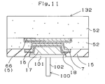
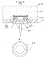
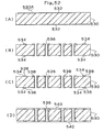
- the foregoing pin is called a "T-type pin" having a T-like side shape realized by a columnar connecting portion 722 and a plate-like secured portion 721 as shown in Fig.76.
- the connecting portion 722 is used to establish the connection with a socket of mother board or the like.
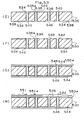
- the foregoing conductive pin 710 is, with a conductive adhesive agent 717, such as solder, bonded and secured to a pad 716 which is a conductive layer of an interlayer resin insulating layer 752 (or a core substrate) which is the outermost layer of the build-up multilayer circuit plate.
- the foregoing structure suffers from an excessively small area of contact between the pad 716 and the interlayer resin insulating layer 752.
- the metal pad and the resin insulating layer are made of different materials. Therefore, there arises a problem in that the strength of adhesive bonding is unsatisfactorily small. Therefore, warp or asperities of the substrate sometimes occur owing to the difference in the coefficiency of thermal expansion between the package substrate and the mother board or the daughter board under a heat cycle condition in which a high temperature and a low temperature are repeated and which is performed as a reliability test. In the foregoing case, fracture of the interface occurs between the pad 716 and the interlayer resin insulating layer 752.
- the conductive connecting pin 720 separates from the substrate together with the substrate.
- displacement between the position of the conductive connecting pin and the socket of the mother board causes stress to be concentrated to the connection portion.
- the conductive connecting pin sometimes separates together with the pad. Heat in the high temperature region in the heat cycle and that generated when the IC chip is mounted, sometimes causes the conductive pin to be separated or inclined. Moreover, the electrical connection cannot sometimes be established.
- an object of the present invention is to provide a conductive connecting pin which is free from concentration of stress under heat cycle conditions or during a mounting an electronic component such as an IC chip and a resin package substrate incorporating the conductive connecting pin which cannot easily be peeled and separated and with which the electrical connection can easily be established if the stress is exerted.
- the build-up multilayer circuit plate for use as a package substrate has a plane layer for constituting a power supply layer to permit supply of large electric power to the IC chip or a plane layer for constituting an earth layer to reduce noise.
- the plane layer is connected to the pad which establishes the connection with an external substrate (for example, a daughter board) through a via hole.
- the plane layer which constitutes the power supply layer for the purpose of supplying electric current from the daughter board portion through the fine via hole is able to supply only limited electric power to the IC chip. Therefore, a satisfactory function cannot be realized.
- the plane layer, which constitutes the earth layer and which is connected to the earth line of the daughter board through the fine via hole having high resistance cannot satisfactorily reduce noise.
- the conductive connecting pin To connect the multilayer printed circuit board for use as the package substrate to the daughter board, the conductive connecting pin must be joined to the pad provided for the multilayer printed circuit board. If a metal pad is provided for the package substrate made of resin, the conductive connecting pin separates together with the pad when stress has been exerted on the conductive connecting pin because the strength of adhesive bonding of each of the two elements is unsatisfactorily low.
- an object of the present invention is to provide a package substrate incorporating a plane layer having a satisfactory function.
- Another object of the present invention is to provide a resin package substrate incorporating a plane layer having a satisfactory function and a conductive connecting pin which cannot easily be separated.
- the build-up multilayer circuit plate incorporates a BGA constituted by solder or the like in order to establish the connection with an external substrate.
- the build-up multilayer circuit plate is mounted on the surface of the external substrate.
- a variety of heat hysteresis experienced with the build-up multilayer circuit board when it is formed such as drying and hardening of the interlayer resin insulating layer and the solder resist (an organic resin insulating layer), drying occurring after a plated film has been formed and an annealing process causes the substrate to be warped or asperities to occur.
- the warp and asperities sometimes inhibit the connection between the build-up multilayer circuit plate and the external substrate by using the small BGA.
- connection with the external substrate by using PGA as a substitute for the BGA of the build-up multilayer circuit plate. That is, the PGA establishes the electrical connection by inserting a pin into a connection portion of the external substrate. Therefore, the foregoing defect in the connection experienced with the BGA does not occur.
- the build-up multilayer circuit plate incorporates the insulating resin layer which does not contain a reinforcing agent made of glass epoxy resin or the like. Therefore, the strength for supporting the PGA is too small to enlarge the tensile strength. What is worse, plating solution which is used to form a conductive layer in the through hole after the drilling operation has been performed, a variety of heat hysteresis or heat required to melt solder in the through hole to secure the PGA sometimes causes the resin in the interlayer insulating layer to be melted. Thus, the PGA cannot sometimes be disposed.
- the PGA Since the PGA requires the through hole to be formed, disposition of an electric line in the lower layer is inhibited which is permitted for the BGA. Therefore, the degree of freedom required when the substrate is designed is narrowed excessively.
- an object of the present invention is to provide a package substrate with which the tensile strength of the PGA is enlarged and the degree of freedom of wiring can be widened and which exhibits a satisfactory connection characteristic with an external substrate.
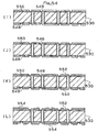
- an first aspect of the present invention has a structure that a pad to which a conductive connecting pin is secured is covered with an organic resin insulating layer having an opening for partially exposing the pad. Therefore, for example, when the package substrate is joined to another substrate, such as a mother board through the conductive connecting pin in a state where, for example, the positions of the conductive connecting pin and the socket of the mother board are sometimes deviated from each other. As an alternative to this, the heat hysteresis of the heat cycle condition sometimes causes the substrate to be warped.
- the size of the pad is somewhat larger than the opening of the organic resin insulating layer through which the pad is exposed.
- the pad is partially exposed to the outside through the foregoing opening. That is, the periphery of the pad is covered with the organic resin insulating layer.
- the size of the pad is 1.02 time to 100 times the diameter of the opening of the organic resin insulating layer through which the pad is exposed to the outside. If the diameter of the pad is smaller than 1.02 of the diameter of the opening, the organic resin insulating layer cannot reliably hold the periphery of the pad. Therefore, separation of the conductive connecting pin cannot be prevented. If the size is larger than 100 times, raising of the density of conductive layer is inhibited. Specifically, when the diameter of the opening formed in the organic resin insulating layer is 100 ⁇ m to 1,500 ⁇ m, the diameter of the pad is 110 ⁇ m to 2,000 ⁇ m.
- a second aspect of the present invention 2 has a structure that an extending portion over the periphery of the pad is covered with an organic resin insulating layer. Therefore, if stress is applied to the conductive connecting pin, separation from the substrate can be prevented because the pad is held by the organic resin insulating layer.
- the body of the pad is exposed to the outside through the opening of the organic resin insulating layer. That is, the organic resin insulating layer and the body of the pad are not in contact with each other. Therefore, the contact between the organic resin insulating layer and the body of the pad does not cause any crack to occur.
- a third aspect of the present invention 5 has a structure that the pad is, through the via hole, joined to the conductive layer which is the inner layer. Therefore, the area of contact between the pad and the substrate is enlarged, causing the two elements to be joined firmly.
- the first aspect has the structure that the pad to which the conductive connecting pin is secured and the interlayer resin insulating layer to which the pad is bonded are bonded to each other as bonding of different materials.
- the third aspect of the present invention has the structure that the pad is connected to the conductive layer which is the inner layer. Therefore, the two elements are connected to each other as the connection of metal elements. Therefore, the connection can furthermore reliably be established. The peeling strength of the pad can be enlarged.
- the pad may be connected to the conductive layer, which is the inner layer, through one or more via holes.
- the reason for this lies in that the area of contact of the pad can furthermore be enlarged to effectively prevent the separation.
- the via hole may be formed into a ring shape and the pad may be disposed to cover the ring.
- the pad to which the conductive connecting pin of the build-up multilayer circuit plate is connected may be so structured as to be connected to the conductive layer, which is the inner layer, through two or more layers of via holes.
- the two or more layers of the via holes may be one via hole according to the shape or the type of the package substrate. In either case, the surface area of the pad can be enlarged to effectively enlarge the strength of adhesive bonding.
- the via hole provided with the pad is covered with the organic resin insulating layer having the opening through which the pad is partially exposed to the outside, separation of the pad can reliably be prevented.
- Another aspect of the present invention has a structure that the conductive layer of the core substrate is made firmly contact with the surface of a resin substrate serving as a core substrate through a coarsened surface (a mat surface).
- a pad is connected to the foregoing conductive layer, the pad cannot easily be separated from the interlayer resin insulating layer.
- the conductive layer which is the inner layer, through one or more via holes and two or more layers of via holes, the conductive layer, which is the inner layer, may be provided for the core substrate.
- the pad is connected to the land around the through hole and a filer filled in the through hole through a via hole.
- so-called “cover plating” may be performed such that the through hole is covered with a conductive layer.
- the pad may be connected to the conductive layer through the via hole.
- the pad may be connected to only the land of the through hole through the via hole.
- the strength of adhesive bonding with the conductive connecting pin can be made to be 2.0 Kg/pin or greater because the melting point of the conductive adhesive agent is 180°C to 280°C.
- the foregoing strength is not considerably reduced even after the reliability test, such as a heat cycle test, or even after heat has been applied during mounting of IC chips. If the melting point is lower than 180°C, realized strength of adhesive bonding is about 2.0 Kg/pin. In some cases, only unsatisfactory strength of adhesive bonding of 1.5 Kg/pin can be realized. What is worse, heating applied during mounting of the IC chips sometimes causes the conductive adhesive agent to be melted. Thus, the conductive connecting pin is undesirably separated and inclined.
- the melting point is higher than 280°C, the resin insulating which is the resin layer and the solder resist layer are unsatisfactory dissolved at a temperature at which the conductive adhesive agent is dissolved. It is preferable that the temperature is 200°C to 260 °C .
- the conductive adhesive agent has the above-mentioned melting point, dispersion of the strength of adhesive bonding of the conductive connecting pin can be reduced. Moreover, applied heat does not damage the resin layer which constitutes the package substrate.
- the conductive adhesive agent is made of at least one type of material selected from tin, lead, antimony, silver, gold and copper. Therefore, the conductive adhesive agent having the above-mentioned melting point can be prepared.
- a conductive adhesive agent containing at least tin-lead or tin-antimony is able to realize the above-mentioned range of the melting point. If the conductive adhesive agent is melted, re-fixation easily occurs. Thus, separation and inclination of the conductive connecting pin do not occur.
- the strength of adhesive bonding can be made to be 2.0 Kg/pin. Moreover, dispersion of the strength of adhesive bonding can be restrained. Even with the heat cycle condition and heat applied during mounting of IC chips, reduction in the strength of adhesive bonding of the conductive connecting pin can be prevented. Moreover, separation and inclination of the pin can be prevented. In addition, also electrical connection can also be maintained.
- the conductive connecting pin is made of at least one type of metal materials selected from copper, a copper alloy, tin, zinc, aluminum and noble metal having excellent flexibility. Therefore, when stress is applied to the pin, the pin is deflected so that the stress is absorbed. As a result, the conductive connecting pin cannot easily be separated from the substrate. It is preferable that the copper alloy for constituting the conductive connecting pin is phosphor bronze which exhibits excellent flexibility and satisfactory electric characteristics and which permits easy processing of the conductive connecting pin.
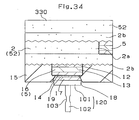
- the conductive connecting pin is a so-called T-type pin incorporating a plate-like secured portion and a columnar connection portion projecting over the central portion of the plate-like secured portion.
- the plate-like secured portion is a portion which is, through the conductive adhesive agent, secured to the conductive layer which is formed into the pad.
- the foregoing plate-like secured portion is formed into an arbitrary shape including a circular shape and a polygonal shape adaptable to the size of the pad.
- the shape of the connection portion is required to permit insertion into another substrate.
- the shape may be any one of a cylindrical shape, a prismatic shape, a conical shape and a pyramid shape.
- one pin is provided for the pin disposed at a usual position. Two or more connection portions may be provided. The number of the connection portions may arbitrarily be determined.
- the columnar connection portion of the conductive connecting pin has a diameter of 0.1 mm to 0.8 mm, the length of 1.0 mm to 10 mm and the diameter of the columnar secured portion is 0.5 mm to 2.0 mm.
- the foregoing values are arbitrarily determined according to the size of the pad and the type or the like of another substrate which must be mounted.
- connection portion is deflected if the stress is applied to the conductive connecting pin because the positions of the conductive connecting pin and the other substrate are deviated from each other. If warp of the substrate or the like occurs owing to heat hysteresis of the heat cycle condition, the secured portion is deflected to correspond to the deformation. Therefore, separation of the conductive connecting pin from the substrate can be prevented. As a result, a reliable package substrate can be obtained.
- the above package substrate may have a structure that a pad, to which the conductive connecting pin is connected, is covered with an organic resin insulating layer having an opening through which the pad is partially exposed.
- an organic resin insulating layer having an opening through which the pad is partially exposed.
- the size of the pad is somewhat larger than that of the opening formed in the organic resin insulating layer through which the pad is exposed to the outside. As a result, the pad can partially be exposed to the outside through the opening. That is, the periphery can be covered with the organic resin insulating layer. It is preferable that the size of the pad is such that the diameter of the pad is 1.02 time to 100 times the diameter of the opening of the organic resin insulating layer through which the pad is exposed to the outside. If the diameter of the pad is smaller than 1.02 time the diameter of the opening, the periphery of the pad cannot reliably be held by the organic resin insulating layer. Therefore, separation of the conductive connecting pin cannot be prevented.
- the diameter is larger than 100 times, raising of the density of the conductive layer is inhibited. Specifically, when the diameter of the opening formed in the organic resin insulating layer is 100 ⁇ m to 1,500 ⁇ m, the diameter of the pad is 110 ⁇ m to 2,000 ⁇ m.
- the conductive connecting pin is made of at least one type of metal selected from copper, a copper alloy, tin, zinc, aluminum and noble metal, exhibiting excellent flexibility.
- the pad for securing the conductive connecting pin is joined to a conductive layer, which is the inner layer, through the via hole.
- the area of contact between the pad and the substrate can be enlarged so that the two elements are firmly joined to each other.
- an aspect has the structure that the pad, to which the conductive connecting pin is secured, and the interlayer resin insulating layer to which the pad is bonded are bonded to each other such that different materials are bonded to each other.
- the aspect claimed in this claim has the structure that the pad is connected to the conductive layer which is the inner layer. Therefore, the two elements are connected to each other as the connection between metal elements. Thus, hermetic contact can furthermore reliably be established and the peeling strength of the pad can be enlarged.
- the pad may be connected to the conductive layer, which is the inner layer, through one or more via holes.
- the reason for this lies in that the area of contact of the pad can furthermore be enlarged. Thus, a structure with which peeling does not easily occur can be realized.
- the pad is connected to the conductive layer, which is the inner layer, through the via hole, it is effective that the via hole is disposed in the periphery of the pad from a viewpoint of improving the connection characteristic. Therefore, a structure may be formed such that the via hole is formed into a ring shape and the pad is disposed to cover the ring.
- the pad of the build-up multilayer circuit plate to which the conductive connecting pin is secured may be so structured as to be connected to the conductive layer, which is the inner layer, through two or more layers of the via holes.
- the two or more layers of the via holes may be constituted by one or more via holes. In either case, the surface area of the pad can be enlarged to effectively enlarge the strength of adhesive bonding.
- Another aspect of the present invention has a structure that the conductive layer on the core substrate is made to hermetically contact with the surface of the resin substrate through the coarsened surface (the mat surface).
- the pad is connected to the foregoing conductive layer, separation of the pad from the interlayer resin insulating layer can furthermore reliably be prevented.
- the conductive layer which is the inner layer, through one or more via holes or two or more layers of the via holes, the conductive layer, which is the inner layer, may be provided for the core substrate.
- Another aspect of the present invention is able to shorten the length of the electric wire from the conductive connecting pin to another substrate disposed on the side surface opposite to the side surface provided with the conductive connecting pin.
- the pad is connected to the land around the through hole and a filer filled in the through hole through a via hole.
- so-called “cover plating” may be performed such that the through hole is covered with a conductive layer.
- the pad may be connected to the conductive layer through the via hole.
- the pad may be connected to only the land of the through hole through the via hole.
- Another aspect of the present invention has a structure that the strength of adhesive bonding with the conductive connecting pin can be made to be 2.0 Kg/pin or greater because the melting point of the conductive adhesive agent is 180 °C to 280 °C.
- the foregoing strength is not considerably reduced even after the reliability test, such as a heat cycle test, or even after heat has been applied during mounting of IC chips. If the melting point is lower than 180°C, realized strength of adhesive bonding is about 2.0 Kg/pin. In some cases, only unsatisfactory strength of adhesive bonding of 1.5 Kg/pin can be realized. What is worse, heating applied during mounting of the IC chips sometimes causes the conductive adhesive agent to be melted. Thus, the conductive connecting pin is undesirably separated and inclined.
- the melting point is higher than 280°C, the resin insulating which is the resin layer and the solder resist layer are unsatisfactorily dissolved at a temperature at which the conductive adhesive agent is dissolved. It is preferable that the temperature is 200°C to 260 °C .
- the conductive adhesive agent has the above-mentioned melting point, dispersion of the strength of adhesive bonding of the conductive connecting pin can be reduced. Moreover, applied heat does not damage the resin layer which constitutes the package substrate.
- the conductive adhesive agent is made of at least one type of material selected fromtin, lead, antimony, silver, gold and copper. Therefore, the conductive adhesive agent having the above-mentioned melting point can be prepared.
- a conductive adhesive agent containing at least tin-lead or tin-antimony is able to realize the above-mentioned range of the melting point. If the conductive adhesive agent is melted, re-fixation easily occurs. Thus, separation and inclination of the conductive connecting pin do not occur.
- the strength of adhesive bonding can be made to be 2.0 Kg/pin. Moreover, dispersion of the strength of adhesive bonding can be restrained. Even with the heat cycle condition and heat applied during mounting of IC chips, reduction in the strength of adhesive bonding of the conductive connecting pin can be prevented. Moreover, separation and inclination of the pin can be prevented. In addition, also electrical connection can be maintained.
- Another aspect of the present invention has a structure that the columnar connection portion of the conductive connecting pin has a constriction portion having a diameter smaller than that of the other portions. Therefore, flexibility is imparted to the pin. Therefore, if stress is applied to the conductive connecting pin, the connection portion is bent at the constriction portion. Therefore, stress can be absorbed so that easy separation of the conductive connecting pin from the substrate is prevented.
- the conductive connecting pin is a so-called T-type pin incorporating a plate-like secured port ion and a columnar connection portion projecting over the central portion of the plate-like secured portion.
- the plate-like secured portion is a portion which is, through the conductive adhesive agent, secured to the conductive layer which is formed into the pad.
- the foregoing plate-like secured portion is formed into an arbitrary shape including a circular shape and a polygonal shape adaptable to the size of the pad.
- the shape of the connection portion is required to permit insertion into another substrate.
- the shape may be any one of a cylindrical shape, a prismatic shape, a conical shape and a pyramid shape.
- one pin is provided for the pin disposed at a usual position.
- Two or more connection portions may be provided. The number of the connection portions may arbitrarily be determined.
- the conductive connecting pin is structured such that the diameter of the plate-like secured portion is 0.5 mm to 2.0 mm, the diameter of the columnar connection portion is 0.1 mm to 0.8 mm and the length is 1 mm to 10 mm.
- the foregoing values are arbitrarily determined according to the size of the package substrate which must be secured and the type or the like of another substrate which must be mounted.
- the constriction portion is formed at an intermediate position of the connection portion such that the diameter of the constriction portion is smaller than the diameter of the other portions.
- the diameter of the constriction portion varies according to the material of the conductive connecting pin and the size of the conductive connecting pin. It is an important fact that the foregoing diameter is not less than 50 % nor more than 98 % of the diameter of the connection portion. If the diameter of the constriction portion is smaller than 50 % of the diameter of the other portions, the strength of the connection portion is unsatisfactory. When the package substrate has been joined, deformation and breakage sometimes occur. If the diameter of the constriction portion is larger than 98 % of the other portion, predetermined flexibility cannot be imparted to the connection portion. Therefore, the effect of absorbing stress cannot be obtained.
- a plurality of the constriction portions may be formed (see Fig. 33 (B)).
- the material of the conductive connecting pin according to the present invention is not limited if the material is a metal material. It is preferable that at least any one of metal materials, such as gold, silver, copper, nickel, cobalt, tin and lead is employed to form the conductive connecting pin. Any one of an iron alloy having trade name "COBAL" (an alloy of Ni-Co-Fe), stainless steel and a phosphor bronze which is a copper alloy is a preferred material because of an external electrical characteristic and satisfactory processability of the conductive connecting pin. Phosphor bronze having external flexibility is able to satisfactorily absorb stress.
- COBAL an alloy of Ni-Co-Fe
- stainless steel and a phosphor bronze which is a copper alloy is a preferred material because of an external electrical characteristic and satisfactory processability of the conductive connecting pin.
- Phosphor bronze having external flexibility is able to satisfactorily absorb stress.
- connection portion is deflected if the stress is applied to the conductive connecting pin because the positions of the conductive connecting pin and the other substrate are deviated from each other. If warp of the substrate or the like occurs owing to heat hysteresis of the heat cycle condition, the secured portion is deflected to correspond to the deformation. Therefore, separation of the conductive connecting pin from the substrate can be prevented. As a result, a reliable package substrate can be obtained.
- a package substrate may have a structure that a pad, to which the conductive connecting pin is connected, is covered with an organic resin insulating layer having an opening through which the pad is partially exposed.
- the size of the pad is somewhat larger than that of the opening formed in the organic resin insulating layer through which the pad is exposed to the outside. As a result, the pad can partially be exposed to the outside through the opening. That is, the periphery can be covered with the organic resin insulating layer. It is preferable that the size of the pad is such that the diameter of the pad is 1.02 time to 100 times the diameter of the opening of the organic resin insulating layer through which the pad is exposed to the outside. If the diameter of the pad is smaller than 1.02 time the diameter of the opening, the periphery of the pad cannot reliably be held by the organic resin insulating layer. Therefore, separation of the conductive connecting pin cannot be prevented.
- the diameter is larger than 100 times, raising of the density of the conductive layer is inhibited. Specifically, when the diameter of the opening formed in the organic resin insulating layer is 100 ⁇ m to 1,500 ⁇ m, the diameter of the pad is 110 ⁇ m to 2,000 ⁇ m.
- connection portion of the conductive connecting pin has a constriction portion to obtain flexibility.
- the pad for securing the conductive connecting pin is joined to the conductive layer, which is the inner layer, through the via hole. Therefore, the area of contact between the pad and the substrate can be enlarged to firmly join the two elements.
- an aspect has the structure that the pad, to which the conductive connecting pin is secured, and the interlayer resin insulating layer to which the pad has been bonded are bonded to each other as bonding between different materials.
- This aspect has the structure that the pad is connected to the conductive layer which is the inner layer. Therefore, the two elements can reliably be made to contact hermeticaly with each other because metal elements are connected to each other. Therefore, the peeling strength of the pad can be enlarged.
- the pad may be connected to the conductive layer, which is the inner layer, through one or more via holes.
- the reason for this lies in that the area of contact of the pad can furthermore be enlarged to effectively prevent the separation.
- the via hole may be formed into a ring shape and the pad may be disposed to cover the ring.
- the pad to which the conductive connecting pin of the build-up multilayer circuit plate is connected may be so structured as to be connected to the conductive layer, which is the inner layer, through two or more layers of via holes.
- the two or more layers of the via holes may be one via hole according to the shape or the type of the package substrate. In either case, the surface area of the pad can be enlarged to effectively enlarge the strength of adhesive bonding.
- the via hole provided with the pad is covered with the organic resin insulating layer having the opening through which the pad is partially exposed to the outside, separation of the pad can reliably be prevented.
- Another aspect of the present invention has a structure that the conductive layer of the core substrate is made to firmly contact with the surface of a resin substrate serving as a core substrate through a coarsened surface (a mat surface).
- a pad is connected to the foregoing conductive layer, the pad cannot easily be separated from the interlayer resin insulating layer.
- the conductive layer which is the inner layer, through one or more via holes and two or more layers of via holes, the conductive layer, which is the inner layer, may be provided for the core substrate.
- the pad is connected to the land around the through hole and a filer filled in the through hole through a via hole.
- so-called “cover plating” may be performed such that the through hole is covered with a conductive layer.
- the pad may be connected to the conductive layer through the via hole.
- the pad may be connected to only the land of the through hole through the via hole.
- the strength of adhesive bonding with the conductive connecting pin can be made to be 2.0 Kg/pin or greater because the melting point of the conductive adhesive agent is 180°C to 280°C.
- the foregoing strength is not considerably reduced even after the reliability test, such as a heat cycle test, or even after heat has been applied during mounting of IC chips. If the melting point is lower than 180°C, realized strength of adhesive bonding is about 2.0 Kg/pin. In some cases, only unsatisfactory strength of adhesive bonding of 1.5 Kg/pin can be realized. What is worse, heating applied during mounting of the IC chips sometimes causes the conductive adhesive agent to be melted. Thus, the conductive connecting pin is undesirably separated and inclined.
- the melting point is higher than 280°C, the resin insulating which is the resin layer and the solder resist layer are unsatisfactorily dissolved at a temperature at which the conductive adhesive agent is dissolved. It is preferable that the temperature is 200°C to 260 °C .
- the conductive adhesive agent has the above-mentioned melting point, dispersion of the strength of adhesive bonding of the conductive connecting pin can be reduced. Moreover, applied heat does not damage the resin layer which constitutes the package substrate.
- the conductive adhesive agent is made of at least one type of material selected from tin, lead, antimony, silver, gold and copper. Therefore, the conductive adhesive agent having the above-mentioned melting point can be prepared.
- a conductive adhesive agent containing at least tin-lead or tin-antimony is able to realize the above-mentioned range of the melting point. If the conductive adhesive agent is melted, re-fixation easily occurs. Thus, separation and inclination of the conductive connecting pin do not occur.
- the strength of adhesive bonding can be made to be 2.0 Kg/pin. Moreover, dispersion of the strength of adhesive bonding can be restrained. Even with the heat cycle condition and heat applied during mounting of IC chips, reduction in the strength of adhesive bonding of the conductive connecting pin can be prevented. Moreover, separation and inclination of the pin can be prevented. In addition, also electrical connection can be maintained.
- a plane layer which is a conductive layer is formed on the surface of the substrate.
- the conductive connecting pin is directly connected to the plane layer so that the electric resistance from an external substrate (for example, a daughter board) to the plane layer is reduced.
- the plane layer constituting the power source layer has a satisfactory function.
- the plane layer constituting the earth layer is connected to the earth line of the daughter board through the conductive connecting pin having low resistance so that the foregoing plane layer has a satisfactory function for preventing noise.
- the plane layer may be formed into a mesh shape.
- the mesh can be formed by forming a square or a circular portion in which no conductor is formed (refer to Fig. 50).
- Another aspect of the present invention has a structure that the pad, to which the conductive connecting pin is secured, is covered with an organic resin insulating layer having an opening through which the pad is partially exposed to the outside.
- the conductive connecting pin is made of at least one type of metal materials selected from copper, a copper alloy, tin, zinc, aluminum and noble metal having excellent flexibility. Therefore, when stress is applied to the pin, the pin is deflected so that the stress is absorbed. As a result, the conductive connecting pin cannot easily be separated from the substrate. It is preferable that the copper alloy for constituting the conductive connecting pin is phosphor bronze which exhibits excellent flexibility and satisfactory electric characteristics and which permits easy processing of the conductive connecting pin.
- the conductive connecting pin is a so-called T-type pin incorporating a plate-like secured portion and a columnar connection portion projecting over the central portion of the plate-like secured portion.
- the plate-like secured portion is a portion which is, through the conductive adhesive agent, secured to the conductive layer which is formed into the pad.
- the foregoing plate-like securedportion is formed into an arbitrary shape including a circular shape and a polygonal shape adaptable to the size of the pad.
- the shape of the connection portion is required to permit insertion into another substrate.
- the shape may be any one of a cylindrical shape, a prismatic shape, a conical shape and a pyramid shape.
- one pin is provided for the pin disposed at a usual position. Two or more connection portions may be provided. The number of the connection portions may arbitrarily be determined.
- the columnar connection portion of the conductive connecting pin has a diameter of 0.1 mm to 0.8 mm, the length of 1.0 mm to 10 mm and the diameter of the columnar secured portion is 0.5 mm to 2.0 mm.
- the foregoing values are arbitrarily determined according to the size of the pad and the type or the like of another substrate which must be mounted.
- Another aspect of the present invention has a structure that the columnar connection portion of the conductive connecting pin has a constriction portion having a diameter smaller than that of the other portions. Therefore, flexibility is imparted to the pin. Therefore, if stress is applied to the conductive connecting pin, the connection portion is bent at the constriction portion. Therefore, stress can be absorbed so that easy separation of the conductive connecting pin from the substrate is prevented.
- the conductive connecting pin is a so-called T-type pin incorporating a plate-like secured portion and a columnar connection portion projecting over the central portion of the plate-like secured portion.
- the plate-like secured portion is a portion which is, through the conductive adhesive agent, secured to the conductive layer which is formed into the pad.
- the foregoing plate-like secured portion is formed into an arbitrary shape including a circular shape and a polygonal shape adaptable to the size of the pad.
- the shape of the connection portion is required to permit insertion into another substrate.
- the shape may be any one of a cylindrical shape, a prismatic shape, a conical shape and a pyramid shape.
- one pin is provided for the pin disposed at a usual position.
- Two or more connection portions may be provided. The number of the connection portions may arbitrarily be determined.
- the conductive connecting pin is structured such that the diameter of the plate-like secured portion is 0.5mm to 2.0mm, the diameter of the columnar connection portion is 0.1 mm to 0.8 mm and the length is 1 mm to 10 mm.
- the foregoing values are arbitrarily determined according to the size of the package substrate which must be secured and the type or the like of another substrate which must be mounted.
- the constriction portion is formed at an intermediate position of the connection portion such that the diameter of the constriction portion is smaller than the diameter of the other portions.
- the diameter of the constriction portion varies according to the material of the conductive connecting pin and the size of the conductive connecting pin. It is an important fact that the foregoing diameter is no less than 50 % nor more than 98 % of the diameter of the connection portion. If the diameter of the constriction portion is smaller than 50 % of the diameter of the other portions, the strength of the connection portion is unsatisfactory. When the package substrate has been joined, deformation and breakage sometimes occur. If the diameter of the constriction portion is larger than 98 % of the other portion, predetermined flexibility cannot be imparted to the connection portion. Therefore, the effect of absorbing stress cannot be obtained.
- a plurality of the constriction portions may be formed.
- the material of the conductive connecting pin according to the present invention is not limited if the material is a metal material. It is preferable that at least any one of metal materials, such as gold, silver, copper, nickel, cobalt, tin and lead is employed to form the conductive connecting pin. Any one of an iron alloy having trade name "COBAL" (an alloy of Ni-Co-Fe), stainless steel andaphosphorbronzewhich is a copper alloy is a preferred material because of an external electrical characteristic and satisfactory processability of the conductive connecting pin. Since phosphor bronze having external flexibility is able to satisfactorily absorb stress.
- COBAL an alloy of Ni-Co-Fe
- stainless steel andaphosphorbronze which is a copper alloy is a preferred material because of an external electrical characteristic and satisfactory processability of the conductive connecting pin. Since phosphor bronze having external flexibility is able to satisfactorily absorb stress.
- Another aspect of the present invention has a structure that the strength of adhesive bonding with the conductive connecting pin can be made to be 2.0 Kg/pin or greater because the melting point of the conductive adhesive agent is 180 °C to 280°C.
- the foregoing strength is not considerably reduced even after the reliability test, such as a heat cycle test, or even after heat has been applied during mounting of IC chips. If the melting point is lower than 180°C, realized strength of adhesive bonding is about 2.0 Kg/pin. In some cases, only unsatisfactory strength of adhesive bonding of 1.5 Kg/pin can be realized. What is worse, heating applied during mounting of the IC chips sometimes causes the conductive adhesive agent to be melted. Thus, the conductive connecting pin is undesirably separated and inclined.
- the melting point is higher than 280°C, the resin insulating which is the resin layer and the solder resist layer are unsatisfactory dissolved at a temperature at which the conductive adhesive agent is dissolved. It is preferable that the temperature is 200°C to 260 °C .
- the conductive adhesive agent has the above-mentioned melting point, dispersion of the strength of adhesive bonding of the conductive connecting pin can be reduced. Moreover, applied heat does not damage the resin layer which constitutes the package substrate.
- the conductive adhesive agent is made of at least one type of material selected fromtin, lead, antimony, silver, gold and copper. Therefore, the conductive adhesive agent having the above-mentioned melting point can be prepared.
- a conductive adhesive agent containing at least tin-lead or tin-antimony is able to realize the above-mentioned range of the melting point. If the conductive adhesive agent is melted, re-fixation easily occurs. Thus, separation and inclination of the conductive connecting pin do not occur.
- the strength of adhesive bonding can be made to be 2.0 Kg/pin. Moreover, dispersion of the strength of adhesive bonding can be restrained. Even with the heat cycle condition and heat applied during mounting of IC chips, reduction in the strength of adhesive bonding of the conductive connecting pin can be prevented. Moreover, separation and inclination of the pin can be prevented. In addition, also electrical connection can be maintained.
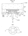
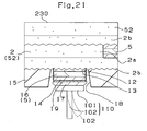
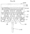
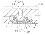
- the projecting pin may be inserted and disposed in a recess formed in the periphery of the opening in the solder resist layer.
- the projecting pin may be disposed through a metal layer or a conductive adhesive layer.
- the electrical connection with the conductor circuit may be established through a recess as a substitute for the opening. Since the electrical connection is established, large-capacity electric power or large-capacity electric signal can be transmitted to an external substrate without any problem.
- the opening must be electrically connected with the conductor circuit of the inner substrate. When a recess is formed around the opening, electrical connection through the recess is not required. If necessary, electrical connection with the conductor circuit may be established.
- the opening in the solder resist layer has a diameter of 100 ⁇ m to 900 ⁇ m. If the diameter is smaller than 100 ⁇ m, the strength of adhesive bonding of the projecting pin is sometimes reduced. If the diameter is larger than 900 ⁇ m, a merit obtainable from the connection with an external substrate by flip-chip mounting can be canceled.
- the diameter of the opening is 120 ⁇ m to 800 ⁇ m.
- Two or more recess each having a diameter of 20 ⁇ m to 100 ⁇ m for connecting the projecting pin are formed around the opening.
- each of the opening and the recesses are formed into a circular shape.
- the reason for this lies in that occurrence of a corner crack can easily be prevented in the opening and a variety of forming methods may be employed.
- Another shape may be employed which includes a rectangular shape and an ecliptic shape.
- the opening and the recesses are formed by any one of a photo-via, laser, drill and punching. It is preferable that photo-via is employed which is capable of simultaneously forming the opening and the recesses.
- the recesses may be formed by etching.
- a metal layer may be formed on the conductor circuit in which the opening is exposed to the outside.
- the metal layer may be constituted by one or more materials selected from a group consisting of gold, silver, nickel, tin, copper, aluminum, lead, phosphorus, chrome, tungsten, molybdenum, titanium, platinum and solder. It is preferable that gold, silver, tin or nickel is employed to form the metal layer. The reason for this lies in that the foregoing metal materials exhibit satisfactory corrosion resistance to prevent corrosion of the exposed conductor circuit.
- the metal layer may be made of one of the foregoing metal material or an alloy with another metal material. Two or more metal layers may be laminated.
- the metal layer may be formed by a method selected from electroless plating, electroplating, substitutional plating, sputtering and evaporation. It is preferable that the electroless plating is employed because a uniform metal film can be formed and the cost can be reduced.
- the conductive adhesive layer is formed by solder, a brazing material, granular substances and thermoplastic resin or granular substances and a thermosetting resin. It is preferable that the adhesive layer is formed by the solder among the foregoing materials. The reason for this lies in that the strength of adhesive bonding can easily be enlarged and a variety of forming methods can be employed.
- the solder which does not include the lead may be used. That reason is that it can be taken into consideration in the environment and moreover strength of adhesive bonding can be secured.
- the forming method is arranged such that printing, potting, resist etching or plating is performed to embed the solder adhesive layer in the opening.
- Another method may be employed with which the adhesive surface of the projecting pin is subj ected to plating or potting to form the solder adhesive layer so as to be melted owing to heat or the like.
- a metal brazing material constituted by one or more materials selected from gold, silver, copper, phosphorus, nickel, palladium, zinc, indium, molybdenum and manganese.
- an eutectic brazing material called a "silver brazing material” or a “gold brazing material” is employed.
- the brazing method is performed such that a brazing material formed into a spherical shape is introduced into the opening so as to be melted so that the adhesive layer is formed. Another method may be employed with which coating of portions except for the opening is performed. Then, immersion is performed so that the material is filled in the opening.
- Another method has the steps of forming a brazing material on the adhesive surface of the projecting metal electrode, performing heating and melting to introduce the brazing material into the opening. As an alternative to this, all usual methods may be employed.
- the adhesive layer is formed by the granular substances and the thermoplastic resin or the thermosetting resin
- the granular substances are made of at least one of metal particles, inorganic particles and resin particles.
- the metal particles of the granular substances may be a metal material, such as copper, gold, silver, nickel, aluminum, titanium, chrome, tin, palladium or platinum. Either of the foregoing metal material may be employed or an alloy of two or more metal materials may be employed.
- the shape of the metal particles may be a spherical shape, a polygonal shape or a mixed shape of the spherical shape and the polygonal shape.
- the inorganic particles of the granular substances may be silica, alumina, mullite or silicon carbide.
- the shape of the inorganic particle may be a spherical shape, a polygonal shape, a porous shape or a mixed shape of the spherical shape and the polygonal shape.
- the surface layer of the inorganic particle is coated with conductive substance substances, such as a metal layer or a conductive resin so that conductivity is imparted to the inorganic particles.
- the resin particles of the granular substances is at least any one of epoxy resin, benzoguanamine resin and amino resin.
- Conductive resin such as anisotropic conductive resin, may be employed to form the inorganic particles.
- the surface layers of the inorganic particles are coated with conductive substances, such as a metal layer or conductive resin, so that conductivity is imparted to the resin particles.
- conductive substances such as a metal layer or conductive resin
- epoxy resin is employed. The reason for this lies in that satisfactory adhesiveness with the formed resin can be realized and the linear expansion coefficients are similar to each other. Therefore, a crack of the formed resin can be prevented.
- the diameter of each of the metal particles, inorganic particles or the resin particles is 0.1 ⁇ m to 50 ⁇ m. If the particle size is smaller than 0.1 ⁇ m, electrical conduction cannot sometimes be established. If the particle size is larger than 50 mm, operability for introducing the particles into the opening deteriorates.
- the filling factor of the metal particles, the inorganic particles or the resin particles with respect to the overall volume is 30 wt% to 90 wt%. If the foregoing factor is lower than 30 wt%, the electrical connection cannot sometimes be established. If the factor is higher than 90 wt%, the strength of adhesive bonding with the projecting pin is reduced.
- the resin for filling the inside portion of the opening may be thermosetting resin or thermoplastic resin.
- the thermosetting resin may be at least one material selected from a group consisting of epoxy resin, polyimide resin, polyester resin and phenol resin.
- the thermoplastic resin maybe at least any one of materials selected from a group consisting of epoxy resin, fluorine-resin polyethylene terephthalate (PET), such as polytetrafluoroethylene (PTFE), ethylene tetrafluoride-propylene hexafluoride copolymer (FEP) or ethylene tetrafluoride perfluoroalkoxy copolymer (PFA); polysulfon (PSF); polyphenylsulfide (PPS); thermoplastic polyphenylether (PPE); polyether sulfon (PES); polyetherimide (PEI); polyphenylsulfon (PPES); polyethylene terephthalate (PEN); polyether etherketone (PEEK); and polyolefine resin.
- PET fluorine-resin polyethylene terephthalate
- PTFE polytetrafluoroethylene
- FEP ethylene tetrafluoride-propylene hexafluoride cop
- the most preferred resin which must be filled in the opening is the epoxy resin.
- the reason for this lies in that any diluting solvent is not required to adjust the viscosity and satisfactory strength, heat resistance and chemical resistance can be realized.
- To adjust the viscosity of the filler resin may be mixed with organic solvent, water, additives and particles.
- the granular substances and the filler resin are mixed by a mixer or the like to uniform the particle substances in the resin. Then, the materials are introduced into the opening.
- thermosetting resin When the thermosetting resin is employed, the resin is filled in the opening by printing or potting. Then, the projecting pin is introduced to cause thermosetting to occur so that joining is performed. To remove air, gaps and excess solvent in the resin, vacuum or reduced-pressure defoaming may be performed. Then, thermosetting may be performed.
- the resin is molded into a tablet shape. Then, the tablets are introduced into the output, and then heating is performed. Then, the projecting pin is inserted. As an alternative to this, the tablets are joined to the bonding surface of the projecting pin, and then heating and melting are performed. Then, the projecting pin is inserted into the opening.
- the number of the projecting pin is basically one. If two or more projecting pins are provided, any problem arises. If two or more projecting pins are provided in parallel, the projecting pins may be disposed around one projecting pin.
- the shape of the projection may be a conical shape, a cylindrical shape, a pyramid shape or a polygonal shape. If the employed shape permits insertion into the connection portion of an external substrate, any shape may be employed.
- the height of the projecting pin satisfies a range from 5 ⁇ m to 50 ⁇ m.
- the ratio of area of the bonding surface of the projecting pin with respect to the diameter of the opening of the solder resist layer is 0.5 to 1.4. In particular, it is preferable that the ratio is 0.8 to 1.2 because the process for bonding the projecting pin to the opening can be facilitated. Moreover, the projecting pin can easily be stood erect at a right angle from the opening.
- the bonding surface may be flat or a shape having projections. That is, when the recesses are formed around the opening, the pin-shape projections may be provided for the bonding surface to enlarge the strength of adhesive bonding of the pin.
- the projecting pin is made of at least any one of the following materials: gold, silver, iron, copper, nickel, cobalt, tin and lead.
- iron, an iron alloy, copper or a copper alloy is employed.
- covar which is an iron alloy, 42-alloy or phosphor bronze has a proven track record as the material for the pin for the PGA.
- the foregoing materials are suitable to a variety of processes for forming projections.
- the projecting pin may be made of a sole metal material, an alloy or formed into a structure covered with a metal layer made of gold, silver or nickel in order to prevent corrosion or a structure covered with a metal layer made of, for example, solder which is melted at a temperature not higher than 250°C in order to enlarge the strength of the adhesive agent.
- the overall body of the projecting pin may be made of metal or the basic structure may be constituted by a nonconductor substances, such as ceramics or nonconductive metal, in order to realize satisfactory strength of the pin. Then, the basic structure is coated with a metal layer so as to establish the electrical connection.
- the conductive adhesive layer, the joint-permissible projecting pin or the metal layer, the conductive adhesive layer and the joint-permissible projecting pin are provided for the opening of the solder resist.
- the projecting pin is inserted into the connection portion of the external substrate so that the conductor circuit formed in the package substrate and the external substrate are electrically connected to each other.
- the projecting pin is so structured as to be inserted into the connection portion of the external substrate. Therefore, when crimping is performed during mounting on the external substrate, concentration of stress to the projecting pin can be relaxed. Therefore, occurrence of a crack and breakage of the conductor circuit or the like which holds the projecting pin can be prevented.
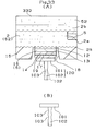
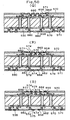
- a package substrate according to a first embodiment will now be described together with a method of manufacturing a build-up substrate. Although the following method is performed by a semi-additive method, a full additive method may be employed.
- a package substrate according to a second embodiment and a manufacturing method therefor will now be described.
- the foregoing steps (1) to (13) are similar to those according to the first embodiment described with reference to Figs. 1. to 5. Therefore, the similar steps are omitted from illustration and description.
- a package substrate according to a third embodiment and a manufacturing method therefor will now be described.
- the foregoing steps (1) to (13) are similar to those according to the first embodiment described with reference to Figs. 1 to 5. Therefore, the similar steps are omitted from illustration and description.
- a package substrate according to a fourth embodiment and a manufacturing method therefor will now be described. Steps (1) to (12) are similar to those according to the first embodiment described with reference to Figs. 1 to 4. Therefore, similar steps are omitted from illustration and description.
- a package substrate according to a fifth embodiment and a manufacturing method therefor will now be described.
- the substrate may be a resin insulating substrate, such as a glass epoxy substrate, a polyimide substrate or a bismaleimide-triazine resin substrate, a copper-clad laminate plate, a ceramic substrate, a metal substrate or the like.
- An interlayer resin insulating layer is provided for the foregoing substrate, and then the interlayer resin insulating layer is coarsened so that a coarsened surface is formed. The overall surface of the coarsened surface is subjected to an electroless plating to have a thin thickness.
- plating resist is formed, and then electrolytic plating is performed to have a large thickness in the portion in which the plating resist is not formed. Then, the plating resist is removed, and then an etching process is performed so that a conductor circuit composed of the electrolytic plated film and an electroless plated film is formed. Either of the conductor circuits is constituted by a copper pattern.
- the substrate having the conductor circuits formed thereon is provided with a recess owing to the conductor circuit or the through hole.
- a resin filler is applied by printing or the like. After the substrate has been dried, excess portion of the resin filler is ground by a grinding operation to expose the conductor circuit to the outside. Then, the resin filler is mainly hardened.
- a coarsened layer is provided for the conductor circuit.
- the coarsened layer is a coarsened surface of copper formed by an etching process, a grinding process, an oxidizing process or an oxidizing and reduction process or a coarsened surface constitute by a plated film.
- the maximum height Ry of the asperities on the coarsened layer is 1 ⁇ m to 10 ⁇ m.
- an interlayer resin insulating layer is formed on the coarsened surface of the conductor circuit.
- the foregoing interlayer resin insulating layer can be formed by using an adhesive agent for electroless plating.
- the adhesive agent for electroless plating constitutes thermosetting resin as the base thereof. If necessary,hardened heat-resisting resin particles, heat-resisting resin particles which are dissolved in acid or an oxidizer, inorganic particles or a fibrous filler may be contained in the foregoing adhesive agent for electroless plating.
- the foregoing resin insulating layer is formed between the lower conductor circuit and the upper conductor circuit so as to be formed into the interlayer resin insulating layer.
- the lower layer is formed into a reinforcing layermade of inorganicparticles, the fibrous filler and a resin base.
- the upper layer may be formed into the adhesive agent layer for electroless plating.
- heat-resisting resin particles which have an average particle size of 0.1 ⁇ m to 2.0 ⁇ m and which may be dissolved in acid or an oxidizer are dispersed in heat-resisting resin which is refractory with respect to acid or the oxidizer to form the lower layer.
- the adhesive agent layer for electroless plating may be formed into the upper layer.
- electroless plated film having a small thickness is formed on the overall surface of the interlayer resin insulating layer which has been coarsened and which have been supplied with catalyst cores. It is preferable that the electroless plated filmmay be an electroless copper plating film having a thickness of 0.5 ⁇ m to 5 ⁇ m, preferably 1 ⁇ m to 3 ⁇ m.
- a photosensitive resin film (a dry film) is laminated on the formed electroless plated film.
- a photomask (it is preferable that a glass substrate is employed) on which a plating resist pattern has been drawn is made in hermetic contact with the surface of the photosensitive resin film so as to be placed on the same. Then, exposure and a development process are performed so that a non-conductor portion having the plating resist pattern is formed.
- an electrolytic plated film is formed in the portion except for the non-conductor portion on the electroless copper plated film.
- a conductor circuit and a conductive portion which is formed into the via hole are formed.
- the electrolytic plating is electrolytic copper plating to have a thickness of 5 ⁇ m to 20 ⁇ m.
- etching solution such as mixed solution of sulfuric acid and peroxide, sodium persulfate, ammonium persulfate, ferric chloride or cupric chloride is used to remove the electroless plated film.
- etching solution such as mixed solution of sulfuric acid and peroxide, sodium persulfate, ammonium persulfate, ferric chloride or cupric chloride is used to remove the electroless plated film.
- the palladium catalyst cores on the coarsened surface exposed over the non-conductor portion is dissolved and removed by chromic acid, sulphated water or the like.
- the coarsened layer is formed on the conductor circuit on the right side of the substrate. It is preferable that the formed coarsened layer is a coarsened layer of copper formed by an etching process, a grinding process, an oxidizing process or an oxidizing and reducing process or a coarsened layer constituted by plated film.
- solder resist layer which is the organic resin insulating layer according to the fifth embodiment is formed on the conductor circuit.
- the thickness of the solder resist layer according to the present invention satisfies a range from 5 ⁇ m to 150 ⁇ m. In particular, it is preferable that the thickness is 5 ⁇ m to 40 ⁇ m.
- the thickness is too small, the function of a solder dam cannot be obtained. If the thickness is too large, the opening cannot easily be formed. Moreover, undesirable contact with the solder occurs, causing a crack to be formed.
- a metal layer constituted by one or more types of materials selected from gold, silver, copper, nickel, tin, aluminum, lead, phosphorus, chrome, tungsten, molybdenum, titanium, platinum and solder may be formed in the opening.
- the metal layer may be formed by any one of plating, evaporating and sputtering capable of forming the metal layer.
- the number of the metal layer may be one or three ormore.
- the metal layer may be omitted.
- the metal layer is constituted by nickel or gold. The reason why the metal layer is formed is that corrosion of the exposed conductor circuit must be prevented.
- a nickel plated layer is formed in the opening by electroless plating.
- the thickness of the nickel plated layer is 0.5 ⁇ m to 20 ⁇ m, more preferably 3 ⁇ m to 10 ⁇ m. If the thickness is too small, the connection between the solder bump and the nickel plated layer cannot easily be established. If the thickness is too large, occupancy of the solder bump formed in the opening is inhibited. In the foregoing case, peeling sometimes occurs.
- gold plating is performed to form a gold plated layer having a thickness of 0.01 ⁇ m to 0.1 ⁇ m, preferably about 0.03 ⁇ m.
- an opening for exposing the conductor circuit is formed or a recess for improving adhesiveness of the projecting pin is formed around the opening.
- the recess is formed by exposing and developing.
- carbon dioxide gas laser, excimer laser or YAG laser is used.
- punching may be employed. A plurality of the foregoing methods maybe employed without any problem.
- the diameter of the opening satisfies a range from 100 mm to 900 mm.
- the diameter of the recess satisfies a range from 5 mm to 70 mm.
- the most suitable shape of the opening and that of the recess are circles.
- the shape may be a polygonal shape, such as a rectangular shape or the shape of a star.
- a conductive adhesive layer is formed in the opening and the recess.
- the adhesive agent maybe solder, a brazing material, conductive granular substances and thermosetting resin or conductive granular substances and thermoplastic resin. It is preferable that solder is employed to form the adhesive layer. The reason for this lies in that great strength of adhesive bonding can be obtained and the forming method can be selected from a variety of methods.
- the adhesive layer is constituted by solder
- a material in which Pb is blended by 35 % to 97 % is employed.
- the solder which does not include the Pb, such as Sn/Sb, Sn/Ag or Sn/Ag/cu may be used.
- the adhesive layer is constituted by the brazing material
- at least one material selected from gold, silver, copper, phosphorus, nickel, palladium, zinc, indium, molybdenum or manganese is employed.
- gold brazing material constituted by a gold alloy or a material called a "silver brazing material" constituted by a silver alloy is employed. The reason for this lies in that satisfactory conductivity can be obtained and corrosion can sufficiently be prevented.
- the granular substances and the thermosetting resin and the thermoplastic resin are used to form the adhesive layer
- the granular substances are constituted by metal, an inorganic material and resin.
- the reason for this lies in that the linear expansion coefficient and the melting point with respect to the resin can easily be adjusted. Moreover, dispersion and coagulation do not easily occur when mixing with resin is performed. Note that substances except for the foregoing substances may be employed.
- the material constituted by the conductive and granular substances, such as metal or the conductive resin is, as it is, or coated with a metal layer is employed as the conductive and granular material.
- the material constituted by the non-conductive substances, such as the inorganic material or the resin, is coated with the metal layer and the conductive, and then used as the conductive and granular substances.
- the foregoing conductive resin is stirred, mixed and uniformly distributed in the thermosetting resin or the thermoplastic resin. Then, the foregoing material is employed to form the adhesive layer.
- the resin is the thermosetting resin. The reason for this lies in that a satisfactory operability can be realized at room temperatures and filling of the opening can be reliably performed.
- the conductive adhesive layer is formed by printing, plating, potting or resist etching.
- the foregoing method is a method for filling the opening in the solder resist with the foregoing material. Another method may be employed with which applying and coating of the foregoing material to the bonding surface of the projecting pin are performed. Then, insertion into the opening is performed.
- the projecting pin is disposed above the opening.
- the number of the projecting pin may be one, or one or more projecting pin may be provided.
- the material may be a metal material, such as gold, silver, iron, nickel, cobalt, tin or lead or a non-conductive material, such as ceramics. In the latter case, conductive metal is used to cove the projecting pin to establish the electrical connection.
- the shape of the bonding surface of the projecting pin may be a flat shape.
- a projection may be provided so as to be inserted into the recess.
- the package substrate according to this embodiment has the structure that when mounting on an external substrate is performed, the projecting pin disposed on the substrate is engaged and connected to the connection portion of the external substrate. Therefore, concentration of stress occurring when heat crimping is performed can be relaxed. As a result, a crack and breakage of the projecting pin and the portion for holding the projecting pin can be prevented.
- Fig. 59 shows the cross section of a package substrate (a package substrate) 510 before an IC chip 590, which is a semiconductor element, is mounted.
- Fig. 60 shows the cross section of the package substrate 510 on which the IC chip 590 has been mounted and which has been joined to a mother board (the external substrate). As shown in Fig. 60, the IC chip 590 has been mounted on the upper surface of the package substrate 510. The lower surface of the package substrate 510 is connected to a daughter board 594.
- the package substrate 510 incorporates a multilayer core substrate 530 having right and reverse sides on which build-up circuit layers 580A and 580B are formed.
- the build-up layer 580A incorporates an interlayer resin insulating layer 550 provided with a via hole 560 and a conductor electric circuit 558; and an interlayer resin insulating layer 650 provided with a via hole 660 and a conductor electric circuit 658.
- the build-up circuit layer 580B incorporates an interlayer resin insulating layer 550 provided with a via hole 560 and a conductor electric circuit 558; and an interlayer resin insulating layer 650 provided with a via hole 660 and a conductor electric circuit 658.
- a projecting pin 576A for establishing the connection with a connection portion 592 (see Fig. 60) of the IC chip 590 is disposed on the upper surface of the package substrate 510.
- a projecting pin 576A for establishing the connection with a connection portion 596 (see Fig. 60) of the daughter board (a sub-board) 594 is disposed on the lower surface.
- the projecting pin 576A is connected to the via hole 660 and the conductor electric circuit 658 through solder 575.
- the projecting pin 576A is provided for the daughter board in this embodiment, a conventional structure may be employed in which a land is provided for the daughter board.
- the projecting pin 576A incorporates conical projections which are inserted into a connection portion 592 of the IC chip 590 and a connection portion 596 of the daughter board 94.
- the projecting pin 576A is made of covar.
- Fig. 61 shows the IC chip before mounting
- Fig. 61 (B) is an enlarged view showing the projecting pin 576A indicated with symbol H shown in Fig. 60.
- connection portion 592 of the IC chip 590 and the projecting pin 576A of the package substrate 510 are located such that the two elements correspond to each other. Then, pressure is applied in a heating state so that the projecting pin 576A is inserted into the connection portion 592 (see Fig. 61 (B)).
- a through hole serving as the connection portion 596 is formed in the daughter board 594.
- the locating of the package substrate 510 and the daughter board is performed (see Fig. 70 (A)), and then pressure is applied to the substrate 10 in a state in which no heat is applied. Then, the projecting pin 576A is inserted into the foregoing through hole (the connection portion) 596 (see Fig. 70 (B)).
- the projecting pin 576A of the package substrate is inserted into an electrode (the connection portion 596) of the daughter board 594.
- stress which is applied when the crimping process is performed can be relaxed. Therefore, occurrence of a crack and breakage of the projecting pin and the holding portion (the solder portion) 575 for the projecting pin at the time of the mounting operation canbe prevented. Since a large joining area is permitted between the projecting pin 576A and the adhesive layer (the solder layer) 575, the strength of adhesive bonding can be enlarged as compared with the conventional structure constituted by the solder bump.
- the projecting pin 576A has one projecting pin 576a as shown in Fig. 71 (A).
- Two or more projecting pins 576C may be provided as shown in Fig. 71 (C) without any problem. If two or more projecting pins are provided, parallel disposition is permitted to surround one projecting pin.
- the shape of the projecting 576a is formed into the conical shape.
- a projecting pin 576B formed into a cylindrical shape as shown in Fig. 71 (B) may be employed.
- the lower surface (the bonding surface) of the projecting pin 576A is flat. If a recess is provided around the opening, a projecting pin 576D formed as shown in Fig. 71 (D) may be employed such that a pin-shape projection 576b is provided for the bonding surface (the bottom surface). Thus, the strength of adhesive bonding of the projecting pin can be enlarged.
- the projecting pin 576A is made of covar and 42-alloy which are iron alloys and phosphor bronze which is a copper alloy.
- the projecting pin 576A is, as shown in Figs. 71 (A), 71 (C) and 71 (D), constituted by one type of metal or an alloy.
- projecting pins 576B and 576E shown in Figs. 71 (B) and 71 (E) may be employed which are made of ceramic 77 in order to enlarge the strength. Then, the surface of the projecting pin is coated with a metal layer.
- a conductor electric circuit 558 composed of the electroless copper plated film and the electrolytic copper plated film and a thickness of 18 ⁇ m and a via hole 560 were formed (step (N) shown in Fig. 55).
- step (N) shown in Fig. 55.
- step (O) the coarsened layer 562 made of Cu-Ni-P was formed.
- step (O) the coarsened layer can be made by the etching (second copper complex and organic acid salt).
- Steps (7) to (15) were repeated so that the upper conductor electric circuit 658 and the via hole 660 (the conductor circuit) were formed.
- step (P) shown in Fig. 55 a multilayer printed circuit board was obtained (step (P) shown in Fig. 55). Note that the Sn substitution was not performed.
- step (P) shown in Fig. 55 46. 67 g of oligomer (having a molecular weight of 4000) which was obtained by forming 50 % of epoxy bases of 60 wt% cresol novolak epoxy resin (manufactured by Nippon Kayaku) dissolved in DMDG into acrylic material and with which was given the photosensitive characteristic, 15.0 g of 80 wt% bis phenol A-type epoxy resin (EPICOAT manufactured by Yuka Shell) dissolved in methyl ethyl ketone, 1.6 g of imidazole hardener (2E4MZ-CN manufactured by Shikoku Kasei), 3 g of polyhydric acrylic monomer (R604 manufactured by Nippon Kayaku) which is photosensitive monomer, 1.5 g of polyhydric acrylic monomer (DPE6A manufactured by Kyoeish
- a drying process was performed at 70°C for 20 minutes and 70°C for 30 minutes.
- a photomask film (not shown) having a circular pattern (a mask pattern) for forming the opening and the recess around the opening and having a thickness of 5mm was disposed in close contact.
- exposure was performed with ultraviolet rays with 500 mJ/cm 2 so that a recess 571b was formed around the opening (step (B) shown in Fig. 62)
- photomask film (not shown) having a circular pattern (a mask pattern) for forming the opening drawn thereon and having a thickness of 5 mm was placed in closed contact.
- a solder resist layer (having a thickness of 20 ⁇ m) 570 was formed (step (Q) shown in Fig. 56).
- the projecting pin 576A constituted by 42-alloy was supported by a pin holding jig (not shown). Then, flux was applied to the inner surface of the opening 571, and then reflowing was performed in a state in which the jig holding the projecting pin 576A was made contact with the package substrate so that the projecting pin 576A was connected to the solder 575.
- a package substrate 510 having the projecting pin metal pin was obtained (see Fig. 57).
- the basic structure was the same as that according to the fifth embodiment.
- a metal layer was formed on the inner surface of the opening.
- Steps (1) to (18) were the same as those according to the fifth embodiment.
- An opening 571 having an opening 571 was formed (step (Q) shown in Fig. 58).
- a nickel layer 572 having a thickness of 5 ⁇ m was provided for the opening.
- the substrate 530 was immersed in an electroless plating solution composed of gold cyanide potassium by 2 g/l, ammonium chloride by 75 g/l, sodium citrate by 50 g/l and sodium hypophosphite by 10 g/l at 93°C for 23 seconds.
- an electroless plating solution composed of gold cyanide potassium by 2 g/l, ammonium chloride by 75 g/l, sodium citrate by 50 g/l and sodium hypophosphite by 10 g/l at 93°C for 23 seconds.
- a gold-plated layer 574 having a thickness of 0.03 ⁇ m was formed on the nickel layer 572 (step (R) shown in Fig. 58) (20)
- the projecting pin 576A constituted by 42-alloy was supported by a pin holding jig (not shown). Then, flux was applied to the inner surface of the opening 571, and then reflowing was performed at 200°C in a state where the jig supporting the projecting pin 576A was made contact with the package substrate so that the connection was established. Thus, a package substrate 510 incorporating the projecting metal pin was obtained (see Fig. 59). (Second Modification)
- the basic structure was the same as that according to the fifth embodiment. Four recesses were formed around each opening 571. Steps (1) to (17) were the same as those according to the fifth embodiment.
- step (A) shown in Fig. 62 Each of the two sides of the multilayer circuit board 10 obtained in step (16) was coated with the solder resist composition 70 to have a thickness of 20 ⁇ m (step (A) shown in Fig. 62). Then, a drying process was performed at 70°C for 20 minutes and 70°C for 30 minutes. A photomask film (not shown) having a circular pattern (amaskpattern) for forming the opening and the recess around the opening and having a thickness of 5 mm was disposed in close contact. Then, exposure was performed with ultraviolet rays with 500 mJ/cm 2 , and then the DMTG development process was performed.
- solder pad portion including the via hole and its land portion
- the solder pad portion was formed into the opening 571 (having a diameter of 150 ⁇ m).
- a solder resist layer (having a thickness of 20 ⁇ m) 70 having four recesses 571b each having a diameter of 10 ⁇ m and a depth of 10 ⁇ m around the opening 571 on the diagonal was formed (step (C) shown in Fig. 62).
- the projecting pin 576D (see Fig. 71 (D)) constituted by 42-alloy was supported by a pin holding jig (not shown). Then, flux was applied to the inner surface of the opening 571, and then reflowing was performed to establish the connection in a state in which the jig supporting the projecting pin 576D was made contact with the package substrate.
- a package substrate 510 having the projecting metal pin was obtained (step (E) shown in Fig. 63).
- the structure was basically the same as that according to the second modification. As shown in Fig. 64, a metal layer was formed in the opening 571. Similarly to the first modification, the metal layer was such that the nickel layer 572 and the gold-plated layer 574 were formed.
- the basic structure was the same as that according to the first modification. As the metal layer, an aluminum layer was formed in the opening. Steps (1) to (18) were the same as those according to the first modification.
- the substrate 530 having the opening 571 formed in the solder resist layer 570 was subjected to the following process: an aluminum layer 672 was, by sputtering, formed on the conductor electric circuit 658 and the via hole 660 through which the opening 571 was exposed to the outside to have a thickness of 4 ⁇ m (step (A) shown in Fig. 65).
- Silver brazing material (BAg-8) 75C in a quantity of 0.1 g was placed on the aluminum layer 672 of the opening 571 so as to be dissolved (step (B) shown in Fig. 65). Then, a projecting pin 576Amade of covar was placed on the dissolved silver brazing material 75C so as to be joined by crimping.
- the basic structure was the same as that according to the fifth embodiment.
- the metal particles in the adhesive layer was copper, while polyimide resin was employed as the thermoplasutic resin.
- Steps (1) to (18) were the same as those according to the first modification.
- the adhesive agent was prepared by using metal particles and thermoplastic resin. Copper which was metal particles was formed into spherical shapes having a diameter of 1 ⁇ m and a diameter of 0.6 ⁇ m, respectively.
- the filling factor was made to be 85 %.
- the molded tablet 675 was inserted into the opening 571 (step (A) shown in Fig. 66), and then the substrate was heated to 200°C. Then, a projecting pin 576A made of covar was placed, and then crimping was performed to perform joining.
- a package substrate was obtained (step (B) shown in Fig. 66).
- the solder resist composition 70 was applied to each side of the multilayer circuit board obtained in step (17) to have a thickness of 20 ⁇ m (step (A) shown in Fig. 67). Then, a drying process was performed at 70°C for 20 minutes and 70°C for 30 minutes. Then, a photomask film (not shown) having a circular pattern (a mask pattern) drawn thereon and a thickness of 5 mm was made in hermetic contact and placed. Then, exposure was performed with ultraviolet rays with 1000 mJ/cm 2 , and then a DMTG development process was performed. Then, a heat process was performed at 80°C for one hour, 100°C for one hour, 120°C for one hour and 150°C for three hours.
- a solder resist layer (having a thickness of 20 ⁇ m) 70 having the opening 571 (having a diameter of 200 ⁇ m) constituted by the solder pad portion (including the via hole and its land portion) was formed (step (B) shown in Fig. 67).
- Two recesses 571b each having a diameter of 50 ⁇ m and a depth of 15 ⁇ m were formed around the opening 571 by using a drill 630 having a diameter of 50 ⁇ m (step (C) shown in Fig. 67).
- the adhesive agent was constituted by inorganic particles and thermosetting resin. Silica in the form of inorganic particles was formed into a polygonal shape having a diameter of 1 ⁇ m.
- the molded inorganic particles were immersed in nickel plating solution, and then the surface layer of the inorganic particle was coated with a nickel layer.
- the inorganic particle coated with nickel was, as the thermosetting resin, stirred in epoxy resin such that coagulation was prevented.
- the filling factor was made to be 90 %.
- the thermosetting resin was injected into a pot for potting such that introduction of air was inhibited. (20) Potting was performed to insert the adhesive agent 75D into the opening 571 (step (D) shown in Fig. 68). Then, heating was performed, and then the projecting pin 576D made of covar was placed. Then, hardening was performed at 200°C so that joining was performed.
- step (E) shown in Fig. 68 The basic structure was the same as that according to the first modification. As shown in Fig. 69 (A), nickel plating 572 was performed as the metal layer. Gold plating was not performed. As the projecting pin 576A, the inner portion was made of covar and the surface layer was constituted by gold plating. Thus, coating with gold was performed. (Eighth Modification) The basic structure was the same as that according to the first modification. As shown in Fig. 71 (E), the projecting pin 57 6E had a structure that the inner portion was made of ceramic 77, the surface layer was formed by nickel and copper coating. Thus, a package substrate was obtained.
- a package substrate according to a ninth modification Referring to Figs. 72 and 73, a package substrate according to a ninth modification will now be described.
- a projecting pin 576F the side surface and bottom surface of which were shown in Fig. 71 (F) is employed.
- the projecting pin 576F has five projections 576b formed over the bottom surface.
- an opening 571 is formed in the solder resist 571 of a package substrate shown in Fig. 72 (A).
- a recess 571b allowed to communicate with a conductor circuit 658 is formed in the opening 571 (Fig. 72 (B)).
- a metal layer 73 made of nickel and so forth is formed in the opening 571 (Fig. 72 (C)).
- the basic structure was the same as that according to the fifth embodiment.
- the electrode formed from the opening was molded as a solder ball so that an IC chip was mounted.
- the package substrates according to the fifth embodiment to the eighth modification and the comparative example were evaluated such that the joining strength, tensile test after the external substrate was mounted (the reliability test), occurrence of a crack and breakage of the electrode were compared. Results were shown in the graph shown in Fig. 74
- the fifth embodiment to the eighth modification were such that the joining strength was 20 Kg/cm 2 or greater, no defective connection of the electrode occurred in the tensile test and the reliability test was resulted in no crack and breakage of the electrode under the heat cycle conditions after 1000 cycles.
- a package substrate according to a sixth embodiment will now be described with reference to Fig. 75.
- the resin multilayer printed circuit board 10 has build-up circuit layers 80U and 80D on the right and reverse sides of the core substrate 30.
- the build-up circuit layers 80U and 80D incorporates a lower interlayer resin insulating layer 50 having a via hole 46, an upper interlayer resin insulating layer 60 having an upper via hole 66 and a solder resist layer 70 formed on the upper interlayer resin insulating layer 60.
- a solder bump (an external connection terminal) 76 for establishing the connection to an IC chip (not shown) is provided for the upper via hole 66 through an opening 71 of the solder resist 70.
- a conductive connecting pin (an external connection terminal) 78 for establishing the connection to a daughter board (not shown) is connected to the lower via hole 66.
- a through hole 36 for connecting the build-up circuit layers 80U and 80D to each other penetrates the core substrate 30 and the lower interlayer resin insulating layer 50.
- the through hole 36 is filled with a resin filler 54.
- Cover plating 58 is applied to the opening.
- the via hole 46 formed in the lower interlayer resin insulating layer 50 is filled with a resin filler 54.
- the opening is applied with cover plating 58.
- a through hole is formed to penetrate the core substrate 30 and the lower interlayer resin insulating layer 50 by drilling or a laser beam so that the through hole 36 is formed.
- the via hole 66 is formed immediately above the through hole 36. Therefore, the through hole 36 and the via hole 66 are disposed in line so that the length of the electric line is shortened. Thus, a signal transmission rate can be raised. Since the through hole 36 and the via hole 66 which is connected to the external connection terminal (a solder pump 76 and a conductive connecting pin 78) are directly connected to each other, satisfactory connection reliability can be realized.
- the sixth embodiment has the structure that a filler 54 enclosed in the through hole 36 is flattened by grinding.
- the cover plating (the conductor layer) 58 is applied.
- the via hole 66 is formed on the cover plating 58. Therefore, the surface of the through hole 36 exhibits satisfactory smoothness. Moreover, satisfactory connection reliability between the through hole 36 and the via hole 66 can be realized.
- the multilayer printed circuit board according to the sixth embodiment has the structure that the same filling resin 54 is enclosed in the through hole 36 and the lower via hole 46.
- the filler resin is simultaneously ground so as to be flattened. Therefore, the cost reduction is permitted.
- the strength of the inside portion of the through hole and that in the via hole can uniformly be maintained. As a result, the reliability of the multilayer printed circuit board can be improved.
- the filler 54 enclosed in the via hole 46 is flattened by grinding, and then the cover plating (the conductor layer) 58 for covering the filler 54 is applied.
- the upper via hole 66 is formed on the cover plating 58. Therefore, the surface of the lower via hole 46 exhibits excellent flatness. Therefore, connection reliability between the lower via hole 46 and the upper via hole 66 can be improved.
- solder layer 77 in the form of Sn/Sb, Sn/Ag or Sn/Ag/Cu is provided.
Landscapes
- Engineering & Computer Science (AREA)
- Microelectronics & Electronic Packaging (AREA)
- Manufacturing & Machinery (AREA)
- Production Of Multi-Layered Print Wiring Board (AREA)
- Lead Frames For Integrated Circuits (AREA)
- Coupling Device And Connection With Printed Circuit (AREA)
- Multi-Conductor Connections (AREA)
- Combinations Of Printed Boards (AREA)
Priority Applications (1)
| Application Number | Priority Date | Filing Date | Title |
|---|---|---|---|
| EP08151537A EP1924130A3 (fr) | 1998-12-16 | 1999-11-17 | Broche de connexion conductrice et substrat d'assemblage |
Applications Claiming Priority (11)
| Application Number | Priority Date | Filing Date | Title |
|---|---|---|---|
| JP35703998A JP2000183532A (ja) | 1998-12-16 | 1998-12-16 | プリント配線板 |
| JP3461699 | 1999-01-04 | ||
| JP9764999 | 1999-04-05 | ||
| JP9765099 | 1999-04-05 | ||
| JP9764899 | 1999-04-05 | ||
| JP10429499 | 1999-04-12 | ||
| JP23193499A JP4458582B2 (ja) | 1999-01-04 | 1999-08-18 | パッケージ基板 |
| JP11231932A JP2000353775A (ja) | 1999-01-04 | 1999-08-18 | 導電性接続ピンおよびパッケージ基板 |
| JP23193399A JP4480207B2 (ja) | 1999-01-04 | 1999-08-18 | 樹脂パッケージ基板 |
| JP23193199A JP4554741B2 (ja) | 1999-01-04 | 1999-08-18 | パッケージ基板 |
| EP99973449A EP1150551B1 (fr) | 1998-12-16 | 1999-11-17 | Tige de connexion conductrice et plaquette de boitier |
Related Parent Applications (1)
| Application Number | Title | Priority Date | Filing Date |
|---|---|---|---|
| EP99973449A Division EP1150551B1 (fr) | 1998-12-16 | 1999-11-17 | Tige de connexion conductrice et plaquette de boitier |
Related Child Applications (1)
| Application Number | Title | Priority Date | Filing Date |
|---|---|---|---|
| EP08151537A Division EP1924130A3 (fr) | 1998-12-16 | 1999-11-17 | Broche de connexion conductrice et substrat d'assemblage |
Publications (2)
| Publication Number | Publication Date |
|---|---|
| EP1720385A2 true EP1720385A2 (fr) | 2006-11-08 |
| EP1720385A3 EP1720385A3 (fr) | 2007-04-18 |
Family
ID=27579868
Family Applications (4)
| Application Number | Title | Priority Date | Filing Date |
|---|---|---|---|
| EP06014707A Ceased EP1720385A3 (fr) | 1998-12-16 | 1999-11-17 | Tige de connexion conductrice et plaquette de circuit de boîtier |
| EP99973449A Expired - Lifetime EP1150551B1 (fr) | 1998-12-16 | 1999-11-17 | Tige de connexion conductrice et plaquette de boitier |
| EP08151537A Withdrawn EP1924130A3 (fr) | 1998-12-16 | 1999-11-17 | Broche de connexion conductrice et substrat d'assemblage |
| EP07106099A Ceased EP1845759A1 (fr) | 1998-12-16 | 1999-11-17 | Broche de connexion conductrice et substrat d'emballage |
Family Applications After (3)
| Application Number | Title | Priority Date | Filing Date |
|---|---|---|---|
| EP99973449A Expired - Lifetime EP1150551B1 (fr) | 1998-12-16 | 1999-11-17 | Tige de connexion conductrice et plaquette de boitier |
| EP08151537A Withdrawn EP1924130A3 (fr) | 1998-12-16 | 1999-11-17 | Broche de connexion conductrice et substrat d'assemblage |
| EP07106099A Ceased EP1845759A1 (fr) | 1998-12-16 | 1999-11-17 | Broche de connexion conductrice et substrat d'emballage |
Country Status (6)
| Country | Link |
|---|---|
| US (5) | US8035214B1 (fr) |
| EP (4) | EP1720385A3 (fr) |
| KR (4) | KR100866814B1 (fr) |
| DE (1) | DE69936319T2 (fr) |
| TW (1) | TW200715918A (fr) |
| WO (1) | WO2000036886A1 (fr) |
Cited By (1)
| Publication number | Priority date | Publication date | Assignee | Title |
|---|---|---|---|---|
| TWI704652B (zh) * | 2019-10-31 | 2020-09-11 | 邱昱維 | 在佈局有電路的陶瓷基板上成形環繞壁的方法及該基板 |
Families Citing this family (67)
| Publication number | Priority date | Publication date | Assignee | Title |
|---|---|---|---|---|
| US7079176B1 (en) | 1991-11-25 | 2006-07-18 | Actv, Inc. | Digital interactive system for providing full interactivity with live programming events |
| US7448063B2 (en) | 1991-11-25 | 2008-11-04 | Actv, Inc. | Digital interactive system for providing full interactivity with live programming events |
| US20020049832A1 (en) | 1996-03-08 | 2002-04-25 | Craig Ullman | Enhanced video programming system and method for incorporating and displaying retrieved integrated internet information segments |
| KR100866814B1 (ko) | 1998-12-16 | 2008-11-04 | 이비덴 가부시키가이샤 | 도전성접속핀 및 패키지기판 |
| DE60023202T2 (de) * | 1999-02-15 | 2006-07-20 | Mitsubishi Gas Chemical Co., Inc. | Leiterplatte für Plastikhalbleitergehäuse |
| US7120871B1 (en) | 1999-09-15 | 2006-10-10 | Actv, Inc. | Enhanced video programming system and method utilizing a web page staging area |
| US7949722B1 (en) | 1999-09-29 | 2011-05-24 | Actv Inc. | Enhanced video programming system and method utilizing user-profile information |
| US7305691B2 (en) | 2001-05-07 | 2007-12-04 | Actv, Inc. | System and method for providing targeted programming outside of the home |
| TWI224382B (en) * | 2001-07-12 | 2004-11-21 | Hitachi Ltd | Wiring glass substrate and manufacturing method thereof, conductive paste and semiconductor module used for the same, and conductor forming method |
| EP1473977A3 (fr) * | 2003-04-28 | 2007-12-19 | Endicott Interconnect Technologies, Inc. | Boîtier électronique avec plots de contact renforcés |
| JP4203666B2 (ja) * | 2004-12-27 | 2009-01-07 | パナソニック株式会社 | 電子部品実装方法および電子部品実装構造 |
| TW200746964A (en) * | 2006-01-27 | 2007-12-16 | Ibiden Co Ltd | Method of manufacturing printed wiring board |
| KR20090100388A (ko) * | 2007-01-16 | 2009-09-23 | 스미토모 베이클리트 컴퍼니 리미티드 | 절연 수지 시트 적층체, 상기 절연 수지 시트 적층체를 적층하여 이루어진 다층 프린트 배선판 |
| US8440916B2 (en) * | 2007-06-28 | 2013-05-14 | Intel Corporation | Method of forming a substrate core structure using microvia laser drilling and conductive layer pre-patterning and substrate core structure formed according to the method |
| JP2009043844A (ja) * | 2007-08-07 | 2009-02-26 | Shinko Electric Ind Co Ltd | リードピン付き配線基板およびリードピン |
| JP2009099589A (ja) * | 2007-10-12 | 2009-05-07 | Elpida Memory Inc | ウエハまたは回路基板およびその接続構造体 |
| TWI393229B (zh) * | 2007-12-04 | 2013-04-11 | Unimicron Technology Corp | 封裝基板的製作方法及其結構 |
| JP4993754B2 (ja) * | 2008-02-22 | 2012-08-08 | 新光電気工業株式会社 | Pga型配線基板及びその製造方法 |
| KR101022942B1 (ko) * | 2008-11-12 | 2011-03-16 | 삼성전기주식회사 | 흐름 방지용 댐을 구비한 인쇄회로기판 및 그 제조방법 |
| US8592691B2 (en) * | 2009-02-27 | 2013-11-26 | Ibiden Co., Ltd. | Printed wiring board |
| KR101070022B1 (ko) * | 2009-09-16 | 2011-10-04 | 삼성전기주식회사 | 다층 세라믹 회로 기판, 다층 세라믹 회로 기판 제조방법 및 이를 이용한 전자 디바이스 모듈 |
| JP5638269B2 (ja) * | 2010-03-26 | 2014-12-10 | 日本特殊陶業株式会社 | 多層配線基板 |
| TWI403223B (zh) * | 2010-05-17 | 2013-07-21 | Nan Ya Printed Circuit Board | 多層印刷電路板電性結構及其製造方法 |
| KR101142339B1 (ko) * | 2010-06-17 | 2012-05-17 | 에스케이하이닉스 주식회사 | 반도체 칩 |
| JP5580135B2 (ja) * | 2010-08-03 | 2014-08-27 | 三井金属鉱業株式会社 | プリント配線板の製造方法及びプリント配線板 |
| US8912653B2 (en) * | 2010-12-30 | 2014-12-16 | Stmicroelectronics Pte Ltd. | Plasma treatment on semiconductor wafers |
| JP2012164965A (ja) * | 2011-01-21 | 2012-08-30 | Ngk Spark Plug Co Ltd | 配線基板及びその製造方法 |
| JP2012169591A (ja) * | 2011-01-24 | 2012-09-06 | Ngk Spark Plug Co Ltd | 多層配線基板 |
| GB201108425D0 (en) * | 2011-05-19 | 2011-07-06 | Zarlink Semiconductor Inc | Integrated circuit package |
| US8829684B2 (en) | 2011-05-19 | 2014-09-09 | Microsemi Semiconductor Limited | Integrated circuit package |
| CN102833945A (zh) * | 2011-06-15 | 2012-12-19 | 景硕科技股份有限公司 | 封装基板结构 |
| US8952540B2 (en) * | 2011-06-30 | 2015-02-10 | Intel Corporation | In situ-built pin-grid arrays for coreless substrates, and methods of making same |
| TWI495051B (zh) * | 2011-07-08 | 2015-08-01 | 欣興電子股份有限公司 | 無核心層之封裝基板及其製法 |
| JP5357241B2 (ja) * | 2011-08-10 | 2013-12-04 | 新光電気工業株式会社 | 半導体装置及び半導体装置の製造方法 |
| DE102011083223B4 (de) * | 2011-09-22 | 2019-08-22 | Infineon Technologies Ag | Leistungshalbleitermodul mit integrierter Dickschichtleiterplatte |
| ITMI20111777A1 (it) * | 2011-09-30 | 2013-03-31 | St Microelectronics Srl | Sistema elettronico per saldatura ad onda |
| JP2013082767A (ja) * | 2011-10-06 | 2013-05-09 | Nitto Denko Corp | 放熱部材およびその製造方法 |
| KR101523840B1 (ko) * | 2012-08-30 | 2015-05-28 | 이비덴 가부시키가이샤 | 프린트 배선판 및 프린트 배선판의 제조 방법 |
| KR101506785B1 (ko) * | 2013-05-29 | 2015-03-27 | 삼성전기주식회사 | 인쇄회로기판 |
| JP2015170770A (ja) * | 2014-03-07 | 2015-09-28 | イビデン株式会社 | プリント配線板 |
| US9706667B2 (en) * | 2014-05-19 | 2017-07-11 | Sierra Circuits, Inc. | Via in a printed circuit board |
| JP2015231003A (ja) * | 2014-06-06 | 2015-12-21 | イビデン株式会社 | 回路基板および回路基板の製造方法 |
| JP6329027B2 (ja) * | 2014-08-04 | 2018-05-23 | ミネベアミツミ株式会社 | フレキシブルプリント基板 |
| JP6274135B2 (ja) * | 2015-03-12 | 2018-02-07 | 株式会社村田製作所 | コイルモジュール |
| CN109560183B (zh) * | 2015-04-29 | 2020-04-17 | 光宝光电(常州)有限公司 | 多层式电路板及发光二极管封装结构 |
| US10187977B2 (en) | 2015-06-29 | 2019-01-22 | Microsoft Technology Licensing, Llc | Head mounted computing device, adhesive joint system and method |
| US10869393B2 (en) | 2015-06-29 | 2020-12-15 | Microsoft Technology Licensing, Llc | Pedestal mounting of sensor system |
| US20170149155A1 (en) * | 2015-11-25 | 2017-05-25 | Mercury Systems, Inc. | Soldered interconnect for a printed circuit board having an angular radial feature |
| CN105430876A (zh) * | 2015-12-29 | 2016-03-23 | 景旺电子科技(龙川)有限公司 | 一种增加金属基板绝缘槽孔孔壁结合力的方法 |
| WO2017171787A1 (fr) * | 2016-03-31 | 2017-10-05 | Intel Corporation | Procédés pour favoriser l'adhérence entre des matériaux diélectriques et conducteurs dans des structures d'emballage |
| US10283445B2 (en) * | 2016-10-26 | 2019-05-07 | Invensas Corporation | Bonding of laminates with electrical interconnects |
| JP2019079902A (ja) * | 2017-10-24 | 2019-05-23 | イビデン株式会社 | プリント配線板 |
| KR102214641B1 (ko) * | 2018-07-16 | 2021-02-10 | 삼성전기주식회사 | 인쇄회로기판 |
| CN109065509A (zh) * | 2018-08-10 | 2018-12-21 | 付伟 | 带有单围堰及外移通孔的芯片封装结构及其制作方法 |
| JP2020087967A (ja) * | 2018-11-15 | 2020-06-04 | イビデン株式会社 | プリント配線板およびその製造方法 |
| EP3709779A1 (fr) * | 2019-03-12 | 2020-09-16 | AT & S Austria Technologie & Systemtechnik Aktiengesellschaft | Support de composant et son procédé de fabrication |
| WO2020215225A1 (fr) * | 2019-04-23 | 2020-10-29 | 庆鼎精密电子(淮安)有限公司 | Carte de circuit imprimé et son procédé de fabrication |
| US11094658B2 (en) * | 2019-05-22 | 2021-08-17 | Lenovo (Singapore) Pte. Ltd. | Substrate, electronic substrate, and method for producing electronic substrate |
| JP2021036554A (ja) * | 2019-08-30 | 2021-03-04 | イビデン株式会社 | プリント配線板の製造方法 |
| US11602800B2 (en) * | 2019-10-10 | 2023-03-14 | Eagle Technology, Llc | Systems and methods for providing an interface on a printed circuit board using pin solder enhancement |
| EP3911132B1 (fr) * | 2020-05-12 | 2024-07-03 | AT & S Austria Technologie & Systemtechnik Aktiengesellschaft | Support de composant comportant un corps solide protégeant un trou de support de composant contre la pénétration de matière étrangère |
| CN114430624B (zh) * | 2020-10-29 | 2024-03-15 | 鹏鼎控股(深圳)股份有限公司 | 电路板的制作方法以及电路板 |
| WO2022097480A1 (fr) | 2020-11-05 | 2022-05-12 | Dic株式会社 | Stratifié pour la fabrication semi-additive et carte de câblage imprimé correspondante |
| CN112867243A (zh) * | 2021-01-06 | 2021-05-28 | 英韧科技(上海)有限公司 | 多层电路板 |
| CN113423183A (zh) * | 2021-07-01 | 2021-09-21 | 定颖电子(昆山)有限公司 | 5g通讯高频信号板制造工艺 |
| US20250063651A1 (en) * | 2022-01-04 | 2025-02-20 | Sumitomo Electric Industries, Ltd. | Printed wiring board and method of manufacturing printed wiring board |
| WO2025094958A1 (fr) * | 2023-10-31 | 2025-05-08 | 京セラ株式会社 | Carte de circuit imprimé, et dispositif à semi-conducteurs |
Citations (3)
| Publication number | Priority date | Publication date | Assignee | Title |
|---|---|---|---|---|
| USRE27934E (en) * | 1971-08-12 | 1974-03-05 | Circuit structure | |
| US5175609A (en) * | 1991-04-10 | 1992-12-29 | International Business Machines Corporation | Structure and method for corrosion and stress-resistant interconnecting metallurgy |
| EP0638931A2 (fr) * | 1993-08-12 | 1995-02-15 | Fujitsu Limited | Module à multi-puce |
Family Cites Families (63)
| Publication number | Priority date | Publication date | Assignee | Title |
|---|---|---|---|---|
| US4418857A (en) * | 1980-12-31 | 1983-12-06 | International Business Machines Corp. | High melting point process for Au:Sn:80:20 brazing alloy for chip carriers |
| JPS5830175A (ja) | 1981-08-17 | 1983-02-22 | Nippon Telegr & Teleph Corp <Ntt> | 超伝導素子実装用装置 |
| JPS58194396A (ja) * | 1982-05-08 | 1983-11-12 | 日本電信電話株式会社 | マイクロピン付配線基板の製法 |
| JPS60250699A (ja) * | 1984-05-25 | 1985-12-11 | 富士通株式会社 | 高周波モジュ−ルの接続構造 |
| JPS61125060A (ja) | 1984-11-22 | 1986-06-12 | Hitachi Ltd | 半導体装置 |
| JPS62173742A (ja) | 1986-01-28 | 1987-07-30 | Fujitsu Ltd | 多層セラミツク回路基板 |
| JPS6388834A (ja) | 1986-10-01 | 1988-04-19 | Hitachi Chem Co Ltd | 半導体素子搭載用配線板 |
| US4880684A (en) | 1988-03-11 | 1989-11-14 | International Business Machines Corporation | Sealing and stress relief layers and use thereof |
| JPH01253940A (ja) | 1988-04-01 | 1989-10-11 | Nec Corp | 半導体装置 |
| USRE34857E (en) * | 1989-05-04 | 1995-02-14 | Kunreuther; Steven J. | Assembly of attachments and device for attaching same |
| JPH0455555A (ja) | 1990-06-25 | 1992-02-24 | Misawa Homes Co Ltd | 建物の手摺支柱の設置構造 |
| JPH04164358A (ja) | 1990-10-29 | 1992-06-10 | Nec Corp | 入出力ピン付き厚膜印刷基板 |
| US5196251A (en) | 1991-04-30 | 1993-03-23 | International Business Machines Corporation | Ceramic substrate having a protective coating thereon and a method for protecting a ceramic substrate |
| JP2967621B2 (ja) * | 1991-08-27 | 1999-10-25 | 日本電気株式会社 | 半導体装置用パッケージの製造方法 |
| JPH0829993B2 (ja) * | 1991-09-23 | 1996-03-27 | インターナショナル・ビジネス・マシーンズ・コーポレイション | セラミツク複合構造及びその製造方法 |
| JP2658672B2 (ja) | 1991-10-11 | 1997-09-30 | 日本電気株式会社 | I/oピンの修理構造および修理方法 |
| JPH05183019A (ja) | 1991-12-27 | 1993-07-23 | Hitachi Ltd | 半導体装置およびその製造方法 |
| US5532031A (en) | 1992-01-29 | 1996-07-02 | International Business Machines Corporation | I/O pad adhesion layer for a ceramic substrate |
| JPH05226052A (ja) * | 1992-02-12 | 1993-09-03 | Nec Corp | セラミック多層配線基板の入出力ピンの形成方法 |
| JP2948990B2 (ja) | 1992-08-26 | 1999-09-13 | 京セラ株式会社 | 半導体素子収納用パッケージ |
| US5313021A (en) * | 1992-09-18 | 1994-05-17 | Aptix Corporation | Circuit board for high pin count surface mount pin grid arrays |
| US5367195A (en) * | 1993-01-08 | 1994-11-22 | International Business Machines Corporation | Structure and method for a superbarrier to prevent diffusion between a noble and a non-noble metal |
| US5371404A (en) * | 1993-02-04 | 1994-12-06 | Motorola, Inc. | Thermally conductive integrated circuit package with radio frequency shielding |
| JPH0761871A (ja) | 1993-08-24 | 1995-03-07 | Ngk Spark Plug Co Ltd | セラミックス基板と外部金属端子との接合構造 |
| US5397598A (en) * | 1993-11-12 | 1995-03-14 | International Business Machines Corporation | Method for selectively coating a member having a shank by masking a portion of the shank with a washer |
| JP2781881B2 (ja) | 1994-09-14 | 1998-07-30 | 株式会社マックエイト | 印刷配線板接続装置 |
| TW281818B (fr) | 1993-12-14 | 1996-07-21 | Market Kk | |
| JPH07273452A (ja) | 1994-03-30 | 1995-10-20 | Ibiden Co Ltd | 多層プリント配線板及びその製造方法 |
| JP3290295B2 (ja) | 1994-05-13 | 2002-06-10 | 太陽インキ製造株式会社 | 硬化性樹脂組成物並びに該組成物を用いた多層プリント配線板及びその製造方法 |
| JPH07326706A (ja) | 1994-05-30 | 1995-12-12 | Fujitsu Ltd | Pga型半導体装置及びその製造方法 |
| JP3432284B2 (ja) * | 1994-07-04 | 2003-08-04 | 三菱電機株式会社 | 半導体装置 |
| JP2565143B2 (ja) | 1994-12-02 | 1996-12-18 | 日本電気株式会社 | 半導体実装基板用素子接合構造およびその製造方法 |
| JPH08172273A (ja) | 1994-12-16 | 1996-07-02 | Hitachi Ltd | セラミック配線基板及びその実装構造体 |
| JPH08195466A (ja) * | 1995-01-17 | 1996-07-30 | Hitachi Ltd | 半導体装置 |
| JPH08213422A (ja) * | 1995-02-07 | 1996-08-20 | Mitsubishi Electric Corp | 半導体装置およびそのボンディングパッド構造 |
| US5714801A (en) | 1995-03-31 | 1998-02-03 | Kabushiki Kaisha Toshiba | Semiconductor package |
| JPH08316367A (ja) | 1995-05-24 | 1996-11-29 | Nec Corp | ピングリッドアレイ |
| US5739584A (en) * | 1995-06-07 | 1998-04-14 | Lsi Logic Corporation | Multiple pin die package |
| JPH098204A (ja) | 1995-06-15 | 1997-01-10 | Ibiden Co Ltd | 半導体パッケージの製造方法 |
| JP3181194B2 (ja) | 1995-06-19 | 2001-07-03 | イビデン株式会社 | 電子部品搭載用基板 |
| JP3037885B2 (ja) | 1995-10-31 | 2000-05-08 | 日本特殊陶業株式会社 | Pga型電子部品用基板 |
| JPH09162320A (ja) * | 1995-12-08 | 1997-06-20 | Shinko Electric Ind Co Ltd | 半導体パッケージおよび半導体装置 |
| JPH09219420A (ja) | 1996-02-14 | 1997-08-19 | Matsushita Electric Ind Co Ltd | 半導体装置 |
| JPH09223719A (ja) * | 1996-02-15 | 1997-08-26 | Matsushita Electric Ind Co Ltd | 半導体装置 |
| JP3317652B2 (ja) | 1996-03-04 | 2002-08-26 | イビデン株式会社 | 多層プリント配線板 |
| US5912510A (en) * | 1996-05-29 | 1999-06-15 | Motorola, Inc. | Bonding structure for an electronic device |
| AU3301197A (en) | 1996-06-05 | 1998-01-05 | Larry W. Burgess | Blind via laser drilling system |
| JPH1022601A (ja) | 1996-07-04 | 1998-01-23 | Hitachi Ltd | 入出力ピンの接続構造 |
| US5700735A (en) * | 1996-08-22 | 1997-12-23 | Taiwan Semiconductor Manufacturing Company, Ltd. | Method of forming bond pad structure for the via plug process |
| JP3224211B2 (ja) | 1996-11-20 | 2001-10-29 | イビデン株式会社 | ソルダーレジスト組成物およびプリント配線板 |
| EP1796446B1 (fr) | 1996-11-20 | 2011-05-11 | Ibiden Co., Ltd. | Circuit imprimé |
| JP3466398B2 (ja) | 1996-12-13 | 2003-11-10 | 日本特殊陶業株式会社 | 配線基板とその製造方法 |
| JP3152633B2 (ja) | 1996-12-19 | 2001-04-03 | イビデン株式会社 | 多層プリント配線板およびその製造方法 |
| JPH10270143A (ja) * | 1997-03-26 | 1998-10-09 | Ibiden Co Ltd | 端子付き基板の製造方法 |
| JPH10270144A (ja) * | 1997-03-26 | 1998-10-09 | Ibiden Co Ltd | 端子付き基板製造用治具 |
| JP3340350B2 (ja) | 1997-04-18 | 2002-11-05 | 富士通株式会社 | 薄膜多層基板及び電子装置 |
| US5965064A (en) * | 1997-10-28 | 1999-10-12 | Sony Chemicals Corporation | Anisotropically electroconductive adhesive and adhesive film |
| US6013877A (en) * | 1998-03-12 | 2000-01-11 | Lucent Technologies Inc. | Solder bonding printed circuit boards |
| KR100866814B1 (ko) | 1998-12-16 | 2008-11-04 | 이비덴 가부시키가이샤 | 도전성접속핀 및 패키지기판 |
| JP3378550B2 (ja) * | 2000-02-03 | 2003-02-17 | 日本特殊陶業株式会社 | リードピン付き配線基板 |
| US6623283B1 (en) * | 2000-03-08 | 2003-09-23 | Autosplice, Inc. | Connector with base having channels to facilitate surface mount solder attachment |
| JP4164358B2 (ja) | 2002-12-27 | 2008-10-15 | キヤノン株式会社 | ファイル保管装置及びプログラム |
| TWI315658B (en) * | 2007-03-02 | 2009-10-01 | Phoenix Prec Technology Corp | Warp-proof circuit board structure |
-
1999
- 1999-11-17 KR KR1020077019759A patent/KR100866814B1/ko not_active Expired - Lifetime
- 1999-11-17 EP EP06014707A patent/EP1720385A3/fr not_active Ceased
- 1999-11-17 DE DE69936319T patent/DE69936319T2/de not_active Expired - Lifetime
- 1999-11-17 KR KR1020017007575A patent/KR100882173B1/ko not_active Expired - Lifetime
- 1999-11-17 US US09/830,949 patent/US8035214B1/en not_active Expired - Fee Related
- 1999-11-17 EP EP99973449A patent/EP1150551B1/fr not_active Expired - Lifetime
- 1999-11-17 WO PCT/JP1999/006428 patent/WO2000036886A1/fr not_active Ceased
- 1999-11-17 KR KR1020067024954A patent/KR100804456B1/ko not_active Expired - Lifetime
- 1999-11-17 EP EP08151537A patent/EP1924130A3/fr not_active Withdrawn
- 1999-11-17 KR KR1020087010076A patent/KR20080043408A/ko not_active Ceased
- 1999-11-17 EP EP07106099A patent/EP1845759A1/fr not_active Ceased
- 1999-12-15 TW TW095147633A patent/TW200715918A/zh unknown
-
2008
- 2008-10-24 US US12/257,501 patent/US7847393B2/en not_active Expired - Fee Related
-
2009
- 2009-01-26 US US12/359,663 patent/US7902659B2/en not_active Expired - Fee Related
- 2009-08-25 US US12/546,950 patent/US8536696B2/en not_active Expired - Fee Related
- 2009-10-19 US US12/581,205 patent/US8110917B2/en not_active Expired - Fee Related
Patent Citations (3)
| Publication number | Priority date | Publication date | Assignee | Title |
|---|---|---|---|---|
| USRE27934E (en) * | 1971-08-12 | 1974-03-05 | Circuit structure | |
| US5175609A (en) * | 1991-04-10 | 1992-12-29 | International Business Machines Corporation | Structure and method for corrosion and stress-resistant interconnecting metallurgy |
| EP0638931A2 (fr) * | 1993-08-12 | 1995-02-15 | Fujitsu Limited | Module à multi-puce |
Cited By (1)
| Publication number | Priority date | Publication date | Assignee | Title |
|---|---|---|---|---|
| TWI704652B (zh) * | 2019-10-31 | 2020-09-11 | 邱昱維 | 在佈局有電路的陶瓷基板上成形環繞壁的方法及該基板 |
Also Published As
| Publication number | Publication date |
|---|---|
| KR100866814B1 (ko) | 2008-11-04 |
| EP1924130A3 (fr) | 2010-11-17 |
| KR20070095458A (ko) | 2007-09-28 |
| TW200715918A (en) | 2007-04-16 |
| EP1150551A4 (fr) | 2004-03-10 |
| US7902659B2 (en) | 2011-03-08 |
| KR100804456B1 (ko) | 2008-02-20 |
| EP1150551A1 (fr) | 2001-10-31 |
| US8536696B2 (en) | 2013-09-17 |
| US20090314537A1 (en) | 2009-12-24 |
| US20090053459A1 (en) | 2009-02-26 |
| KR100882173B1 (ko) | 2009-02-06 |
| US8110917B2 (en) | 2012-02-07 |
| EP1845759A1 (fr) | 2007-10-17 |
| DE69936319T2 (de) | 2008-02-14 |
| WO2000036886A1 (fr) | 2000-06-22 |
| US7847393B2 (en) | 2010-12-07 |
| EP1720385A3 (fr) | 2007-04-18 |
| EP1150551B1 (fr) | 2007-06-13 |
| KR20010093184A (ko) | 2001-10-27 |
| DE69936319D1 (de) | 2007-07-26 |
| EP1924130A2 (fr) | 2008-05-21 |
| US20100032200A1 (en) | 2010-02-11 |
| US20090154131A1 (en) | 2009-06-18 |
| KR20080043408A (ko) | 2008-05-16 |
| US8035214B1 (en) | 2011-10-11 |
| KR20060130270A (ko) | 2006-12-18 |
Similar Documents
| Publication | Publication Date | Title |
|---|---|---|
| EP1150551B1 (fr) | Tige de connexion conductrice et plaquette de boitier | |
| US7995352B2 (en) | Printed circuit board | |
| EP1194022B1 (fr) | Carte a circuit imprime multicouche et procede de fabrication d'une telle carte | |
| JP2001332437A (ja) | コンデンサおよび多層プリント配線板 | |
| JP2002170840A (ja) | 半導体素子及び半導体素子を内蔵する多層プリント配線板の製造方法 | |
| JP4343390B2 (ja) | プリント配線板用導体ピン、多層プリント配線板 | |
| JP4480207B2 (ja) | 樹脂パッケージ基板 | |
| JP2002305377A (ja) | 多層プリント配線板 | |
| JP2002185145A (ja) | 多層プリント配線板およびその製造方法 | |
| JP2000183532A (ja) | プリント配線板 | |
| JP4743974B2 (ja) | 樹脂フィルムおよび多層プリント配線板の製造方法 | |
| JP4554741B2 (ja) | パッケージ基板 | |
| JP2000353775A (ja) | 導電性接続ピンおよびパッケージ基板 |
Legal Events
| Date | Code | Title | Description |
|---|---|---|---|
| PUAI | Public reference made under article 153(3) epc to a published international application that has entered the european phase |
Free format text: ORIGINAL CODE: 0009012 |
|
| AC | Divisional application: reference to earlier application |
Ref document number: 1150551 Country of ref document: EP Kind code of ref document: P |
|
| AK | Designated contracting states |
Kind code of ref document: A2 Designated state(s): AT BE CH CY DE DK ES FI FR GB GR IE IT LI LU MC NL PT SE |
|
| 17P | Request for examination filed |
Effective date: 20061002 |
|
| PUAL | Search report despatched |
Free format text: ORIGINAL CODE: 0009013 |
|
| AK | Designated contracting states |
Kind code of ref document: A3 Designated state(s): AT BE CH CY DE DK ES FI FR GB GR IE IT LI LU MC NL PT SE |
|
| 17Q | First examination report despatched |
Effective date: 20070903 |
|
| AKX | Designation fees paid |
Designated state(s): DE FI GB NL |
|
| STAA | Information on the status of an ep patent application or granted ep patent |
Free format text: STATUS: THE APPLICATION HAS BEEN REFUSED |
|
| 18R | Application refused |
Effective date: 20130407 |