EP2418685A2 - Halbleiterbauelemente mit Schottky-Dioden mit gesteuertem Durchbruch und Herstellungsverfahren dafür - Google Patents
Halbleiterbauelemente mit Schottky-Dioden mit gesteuertem Durchbruch und Herstellungsverfahren dafür Download PDFInfo
- Publication number
- EP2418685A2 EP2418685A2 EP11187310A EP11187310A EP2418685A2 EP 2418685 A2 EP2418685 A2 EP 2418685A2 EP 11187310 A EP11187310 A EP 11187310A EP 11187310 A EP11187310 A EP 11187310A EP 2418685 A2 EP2418685 A2 EP 2418685A2
- Authority
- EP
- European Patent Office
- Prior art keywords
- region
- semiconductor layer
- schottky junction
- junction
- semiconductor
- Prior art date
- Legal status (The legal status is an assumption and is not a legal conclusion. Google has not performed a legal analysis and makes no representation as to the accuracy of the status listed.)
- Granted
Links
Images


Classifications
-
- H—ELECTRICITY
- H10—SEMICONDUCTOR DEVICES; ELECTRIC SOLID-STATE DEVICES NOT OTHERWISE PROVIDED FOR
- H10D—INORGANIC ELECTRIC SEMICONDUCTOR DEVICES
- H10D62/00—Semiconductor bodies, or regions thereof, of devices having potential barriers
- H10D62/10—Shapes, relative sizes or dispositions of the regions of the semiconductor bodies; Shapes of the semiconductor bodies
- H10D62/102—Constructional design considerations for preventing surface leakage or controlling electric field concentration
- H10D62/103—Constructional design considerations for preventing surface leakage or controlling electric field concentration for increasing or controlling the breakdown voltage of reverse-biased devices
- H10D62/105—Constructional design considerations for preventing surface leakage or controlling electric field concentration for increasing or controlling the breakdown voltage of reverse-biased devices by having particular doping profiles, shapes or arrangements of PN junctions; by having supplementary regions, e.g. junction termination extension [JTE]
- H10D62/106—Constructional design considerations for preventing surface leakage or controlling electric field concentration for increasing or controlling the breakdown voltage of reverse-biased devices by having particular doping profiles, shapes or arrangements of PN junctions; by having supplementary regions, e.g. junction termination extension [JTE] having supplementary regions doped oppositely to or in rectifying contact with regions of the semiconductor bodies, e.g. guard rings with PN or Schottky junctions
-
- H—ELECTRICITY
- H10—SEMICONDUCTOR DEVICES; ELECTRIC SOLID-STATE DEVICES NOT OTHERWISE PROVIDED FOR
- H10D—INORGANIC ELECTRIC SEMICONDUCTOR DEVICES
- H10D62/00—Semiconductor bodies, or regions thereof, of devices having potential barriers
- H10D62/10—Shapes, relative sizes or dispositions of the regions of the semiconductor bodies; Shapes of the semiconductor bodies
- H10D62/102—Constructional design considerations for preventing surface leakage or controlling electric field concentration
- H10D62/103—Constructional design considerations for preventing surface leakage or controlling electric field concentration for increasing or controlling the breakdown voltage of reverse-biased devices
- H10D62/105—Constructional design considerations for preventing surface leakage or controlling electric field concentration for increasing or controlling the breakdown voltage of reverse-biased devices by having particular doping profiles, shapes or arrangements of PN junctions; by having supplementary regions, e.g. junction termination extension [JTE]
-
- H—ELECTRICITY
- H10—SEMICONDUCTOR DEVICES; ELECTRIC SOLID-STATE DEVICES NOT OTHERWISE PROVIDED FOR
- H10D—INORGANIC ELECTRIC SEMICONDUCTOR DEVICES
- H10D62/00—Semiconductor bodies, or regions thereof, of devices having potential barriers
- H10D62/80—Semiconductor bodies, or regions thereof, of devices having potential barriers characterised by the materials
- H10D62/83—Semiconductor bodies, or regions thereof, of devices having potential barriers characterised by the materials being Group IV materials, e.g. B-doped Si or undoped Ge
- H10D62/832—Semiconductor bodies, or regions thereof, of devices having potential barriers characterised by the materials being Group IV materials, e.g. B-doped Si or undoped Ge being Group IV materials comprising two or more elements, e.g. SiGe
- H10D62/8325—Silicon carbide
-
- H—ELECTRICITY
- H10—SEMICONDUCTOR DEVICES; ELECTRIC SOLID-STATE DEVICES NOT OTHERWISE PROVIDED FOR
- H10D—INORGANIC ELECTRIC SEMICONDUCTOR DEVICES
- H10D8/00—Diodes
- H10D8/01—Manufacture or treatment
- H10D8/051—Manufacture or treatment of Schottky diodes
-
- H—ELECTRICITY
- H10—SEMICONDUCTOR DEVICES; ELECTRIC SOLID-STATE DEVICES NOT OTHERWISE PROVIDED FOR
- H10D—INORGANIC ELECTRIC SEMICONDUCTOR DEVICES
- H10D8/00—Diodes
- H10D8/60—Schottky-barrier diodes
-
- H—ELECTRICITY
- H10—SEMICONDUCTOR DEVICES; ELECTRIC SOLID-STATE DEVICES NOT OTHERWISE PROVIDED FOR
- H10P—GENERIC PROCESSES OR APPARATUS FOR THE MANUFACTURE OR TREATMENT OF DEVICES COVERED BY CLASS H10
- H10P30/00—Ion implantation into wafers, substrates or parts of devices
- H10P30/20—Ion implantation into wafers, substrates or parts of devices into semiconductor materials, e.g. for doping
- H10P30/202—Ion implantation into wafers, substrates or parts of devices into semiconductor materials, e.g. for doping characterised by the semiconductor materials
- H10P30/204—Ion implantation into wafers, substrates or parts of devices into semiconductor materials, e.g. for doping characterised by the semiconductor materials into Group IV semiconductors
- H10P30/2042—Ion implantation into wafers, substrates or parts of devices into semiconductor materials, e.g. for doping characterised by the semiconductor materials into Group IV semiconductors into crystalline silicon carbide
-
- H—ELECTRICITY
- H10—SEMICONDUCTOR DEVICES; ELECTRIC SOLID-STATE DEVICES NOT OTHERWISE PROVIDED FOR
- H10P—GENERIC PROCESSES OR APPARATUS FOR THE MANUFACTURE OR TREATMENT OF DEVICES COVERED BY CLASS H10
- H10P30/00—Ion implantation into wafers, substrates or parts of devices
- H10P30/20—Ion implantation into wafers, substrates or parts of devices into semiconductor materials, e.g. for doping
- H10P30/21—Ion implantation into wafers, substrates or parts of devices into semiconductor materials, e.g. for doping of electrically active species
Definitions
- the present invention relates to semiconductor devices and the fabrication of semiconductor devices and more particularly, to Junction Barrier Schottky (JBS) diodes, and the fabrication of such diodes.
- JBS Junction Barrier Schottky
- the semiconductor layer may include a silicon carbide semiconductor layer.
- the first doped region may include p-type silicon carbide having a dopant concentration of from about 1 x 10 17 to about 1 x 10 18 cm -3
- the second doped region may include p-type silicon carbide having a dopant concentration of greater than about 5 x 10 18 cm -3 .
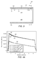
- Figure 6 is a graph of blocking voltage versus doping for JBS diodes according to some embodiments of the invention.
- An anode contact 118 on the surface of the drift layer 114 forms a Schottky junction J4 with the exposed portions 114A of the drift layer 114 between adjacent lightly doped regions 130 and/or between a lightly doped region 130 and the heavily doped region 116.
- the anode contact 118 may include a metal, such as aluminum, titanium and/or nickel, that may form an ohmic contact with the heavily doped region 116, while forming a Schottky contact with the drift layer 114.
Landscapes
- Electrodes Of Semiconductors (AREA)
Applications Claiming Priority (2)
| Application Number | Priority Date | Filing Date | Title |
|---|---|---|---|
| US11/496,842 US7728402B2 (en) | 2006-08-01 | 2006-08-01 | Semiconductor devices including schottky diodes with controlled breakdown |
| EP07112298.0A EP1885000B1 (de) | 2006-08-01 | 2007-07-11 | Halbleiterbauelemente mit Schottky-Dioden mit gesteuertem Durchbruch und Herstellungsverfahren dafür |
Related Parent Applications (3)
| Application Number | Title | Priority Date | Filing Date |
|---|---|---|---|
| EP07112298.0A Division-Into EP1885000B1 (de) | 2006-08-01 | 2007-07-11 | Halbleiterbauelemente mit Schottky-Dioden mit gesteuertem Durchbruch und Herstellungsverfahren dafür |
| EP07112298.0A Division EP1885000B1 (de) | 2006-08-01 | 2007-07-11 | Halbleiterbauelemente mit Schottky-Dioden mit gesteuertem Durchbruch und Herstellungsverfahren dafür |
| EP07112298.0 Division | 2007-07-11 |
Publications (3)
| Publication Number | Publication Date |
|---|---|
| EP2418685A2 true EP2418685A2 (de) | 2012-02-15 |
| EP2418685A3 EP2418685A3 (de) | 2012-05-23 |
| EP2418685B1 EP2418685B1 (de) | 2020-05-06 |
Family
ID=38572841
Family Applications (2)
| Application Number | Title | Priority Date | Filing Date |
|---|---|---|---|
| EP07112298.0A Active EP1885000B1 (de) | 2006-08-01 | 2007-07-11 | Halbleiterbauelemente mit Schottky-Dioden mit gesteuertem Durchbruch und Herstellungsverfahren dafür |
| EP11187310.5A Active EP2418685B1 (de) | 2006-08-01 | 2007-07-11 | Halbleiterbauelemente mit Schottky-Dioden mit gesteuertem Durchbruch und Herstellungsverfahren dafür |
Family Applications Before (1)
| Application Number | Title | Priority Date | Filing Date |
|---|---|---|---|
| EP07112298.0A Active EP1885000B1 (de) | 2006-08-01 | 2007-07-11 | Halbleiterbauelemente mit Schottky-Dioden mit gesteuertem Durchbruch und Herstellungsverfahren dafür |
Country Status (3)
| Country | Link |
|---|---|
| US (2) | US7728402B2 (de) |
| EP (2) | EP1885000B1 (de) |
| JP (2) | JP5415679B2 (de) |
Families Citing this family (70)
| Publication number | Priority date | Publication date | Assignee | Title |
|---|---|---|---|---|
| JP5362187B2 (ja) * | 2006-03-30 | 2013-12-11 | 日本碍子株式会社 | 半導体素子 |
| US7728402B2 (en) * | 2006-08-01 | 2010-06-01 | Cree, Inc. | Semiconductor devices including schottky diodes with controlled breakdown |
| US8432012B2 (en) * | 2006-08-01 | 2013-04-30 | Cree, Inc. | Semiconductor devices including schottky diodes having overlapping doped regions and methods of fabricating same |
| US8710510B2 (en) * | 2006-08-17 | 2014-04-29 | Cree, Inc. | High power insulated gate bipolar transistors |
| DE102006050360B4 (de) | 2006-10-25 | 2014-05-15 | Infineon Technologies Austria Ag | Verfahren zum Erzeugen eines elektrischen Kontakts auf SiC |
| DE102007009227B4 (de) * | 2007-02-26 | 2009-01-02 | Infineon Technologies Ag | Halbleiterbauelement mit gleichrichtenden Übergängen sowie Herstellungsverfahren zur Herstellung desselben |
| US8835987B2 (en) * | 2007-02-27 | 2014-09-16 | Cree, Inc. | Insulated gate bipolar transistors including current suppressing layers |
| DE102007024461B4 (de) * | 2007-05-25 | 2012-10-11 | Infineon Technologies Austria Ag | Halbleiterelement und Verfahren zu seiner Herstellung |
| US8232558B2 (en) | 2008-05-21 | 2012-07-31 | Cree, Inc. | Junction barrier Schottky diodes with current surge capability |
| US8124981B2 (en) * | 2008-06-10 | 2012-02-28 | Fairchild Semiconductor Corporation | Rugged semiconductor device architecture |
| EP2154726A3 (de) * | 2008-08-14 | 2010-05-26 | Acreo AB | Verfahren zur Herstellung einer JBS Diode |
| JP2010087195A (ja) * | 2008-09-30 | 2010-04-15 | Panasonic Corp | 半導体装置 |
| US8294507B2 (en) | 2009-05-08 | 2012-10-23 | Cree, Inc. | Wide bandgap bipolar turn-off thyristor having non-negative temperature coefficient and related control circuits |
| US7915703B2 (en) * | 2009-05-13 | 2011-03-29 | Cree, Inc. | Schottky diodes containing high barrier metal islands in a low barrier metal layer and methods of forming the same |
| US8629509B2 (en) * | 2009-06-02 | 2014-01-14 | Cree, Inc. | High voltage insulated gate bipolar transistors with minority carrier diverter |
| US8193848B2 (en) | 2009-06-02 | 2012-06-05 | Cree, Inc. | Power switching devices having controllable surge current capabilities |
| US8541787B2 (en) * | 2009-07-15 | 2013-09-24 | Cree, Inc. | High breakdown voltage wide band-gap MOS-gated bipolar junction transistors with avalanche capability |
| US8354690B2 (en) | 2009-08-31 | 2013-01-15 | Cree, Inc. | Solid-state pinch off thyristor circuits |
| US9466674B2 (en) * | 2010-03-08 | 2016-10-11 | Cree, Inc. | Semiconductor devices with non-implanted barrier regions and methods of fabricating same |
| US9117739B2 (en) * | 2010-03-08 | 2015-08-25 | Cree, Inc. | Semiconductor devices with heterojunction barrier regions and methods of fabricating same |
| US8415671B2 (en) | 2010-04-16 | 2013-04-09 | Cree, Inc. | Wide band-gap MOSFETs having a heterojunction under gate trenches thereof and related methods of forming such devices |
| JP5550589B2 (ja) * | 2011-03-23 | 2014-07-16 | 株式会社東芝 | 半導体装置 |
| US9029945B2 (en) | 2011-05-06 | 2015-05-12 | Cree, Inc. | Field effect transistor devices with low source resistance |
| US9142662B2 (en) | 2011-05-06 | 2015-09-22 | Cree, Inc. | Field effect transistor devices with low source resistance |
| US9640617B2 (en) | 2011-09-11 | 2017-05-02 | Cree, Inc. | High performance power module |
| US9373617B2 (en) | 2011-09-11 | 2016-06-21 | Cree, Inc. | High current, low switching loss SiC power module |
| WO2013036370A1 (en) | 2011-09-11 | 2013-03-14 | Cree, Inc. | High current density power module comprising transistors with improved layout |
| US8664665B2 (en) | 2011-09-11 | 2014-03-04 | Cree, Inc. | Schottky diode employing recesses for elements of junction barrier array |
| US8680587B2 (en) | 2011-09-11 | 2014-03-25 | Cree, Inc. | Schottky diode |
| US8618582B2 (en) | 2011-09-11 | 2013-12-31 | Cree, Inc. | Edge termination structure employing recesses for edge termination elements |
| US8809902B2 (en) | 2011-10-17 | 2014-08-19 | Infineon Technologies Austria Ag | Power semiconductor diode, IGBT, and method for manufacturing thereof |
| JP5777487B2 (ja) * | 2011-10-28 | 2015-09-09 | 株式会社日立製作所 | 半導体回路 |
| KR20130049919A (ko) * | 2011-11-07 | 2013-05-15 | 현대자동차주식회사 | 실리콘카바이드 쇼트키 배리어 다이오드 소자 및 이의 제조 방법 |
| CA2872941C (en) * | 2012-05-17 | 2021-03-30 | General Electric Company | Semiconductor device with junction termination extension |
| DE102013010187B4 (de) | 2012-06-27 | 2024-11-28 | Fairchild Semiconductor Corp. | Schottky-Barriere-Vorrichtung mit lokal planarisierter Oberfläche und zugehöriges Halbleitererzeugnis |
| US8901639B2 (en) | 2012-07-26 | 2014-12-02 | Cree, Inc. | Monolithic bidirectional silicon carbide switching devices |
| US8969994B2 (en) * | 2012-08-14 | 2015-03-03 | Avogy, Inc. | Method of fabricating a gallium nitride merged P-i-N Schottky (MPS) diode by regrowth and etch back |
| US20140048903A1 (en) * | 2012-08-15 | 2014-02-20 | Avogy, Inc. | Method and system for edge termination in gan materials by selective area implantation doping |
| JP6029397B2 (ja) | 2012-09-14 | 2016-11-24 | 三菱電機株式会社 | 炭化珪素半導体装置 |
| TWI521718B (zh) | 2012-12-20 | 2016-02-11 | 財團法人工業技術研究院 | 接面位障蕭特基二極體嵌於金氧半場效電晶體單元陣列之整合元件 |
| JP2014236171A (ja) | 2013-06-05 | 2014-12-15 | ローム株式会社 | 半導体装置およびその製造方法 |
| CN104282732B (zh) | 2013-07-01 | 2017-06-27 | 株式会社东芝 | 半导体装置 |
| KR20150026531A (ko) | 2013-09-03 | 2015-03-11 | 삼성전자주식회사 | 반도체 장치 그 제조 방법 |
| JP5940500B2 (ja) | 2013-09-11 | 2016-06-29 | 株式会社東芝 | 半導体装置及びその製造方法 |
| US9123828B2 (en) * | 2013-11-14 | 2015-09-01 | Infineon Technologies Ag | Semiconductor device and method for forming a semiconductor device |
| WO2016091488A1 (en) * | 2014-12-08 | 2016-06-16 | Abb Technology Ag | Method for manufacturing a wide bandgap junction barrier schottky diode |
| DE102015101966B4 (de) * | 2015-02-11 | 2021-07-08 | Infineon Technologies Austria Ag | Verfahren zum Herstellen eines Halbleiterbauelements mit Schottkykontakt und Halbleiterbauelement |
| US9741873B2 (en) | 2015-03-27 | 2017-08-22 | Fairchild Semiconductor Corporation | Avalanche-rugged silicon carbide (SiC) power Schottky rectifier |
| US10026805B2 (en) | 2015-03-27 | 2018-07-17 | Farichild Semiconductor Corporation | Avalanche-rugged silicon carbide (SiC) power device |
| US10326509B2 (en) * | 2015-05-28 | 2019-06-18 | Qualcomm Incorporated | Link budget enhancements for single receiver devices |
| JP6400544B2 (ja) * | 2015-09-11 | 2018-10-03 | 株式会社東芝 | 半導体装置 |
| US9960247B2 (en) * | 2016-01-19 | 2018-05-01 | Ruigang Li | Schottky barrier structure for silicon carbide (SiC) power devices |
| EP3497471B1 (de) * | 2016-08-12 | 2021-11-24 | Sony Depthsensing Solutions | Demodulator mit einer ladungsträgererzeugenden gepinnten photodiode |
| BE1025050B1 (fr) * | 2016-08-12 | 2018-10-12 | Softkinetic Sensors Nv | Démodulateur doté d’une photodiode pincée génératrice de porteurs et procédé de fonctionnement associé |
| CN106847922A (zh) * | 2017-01-24 | 2017-06-13 | 深圳基本半导体有限公司 | 一种宽禁带半导体器件 |
| KR102463180B1 (ko) * | 2018-05-04 | 2022-11-03 | 현대자동차 주식회사 | 반도체 소자 및 그 제조 방법 |
| KR102507841B1 (ko) * | 2018-05-04 | 2023-03-07 | 현대자동차 주식회사 | 반도체 소자 및 그 제조 방법 |
| CN109888024B (zh) * | 2018-12-29 | 2024-04-02 | 厦门芯光润泽科技有限公司 | Mps二极管器件及其制备方法 |
| CN109860273B (zh) * | 2018-12-29 | 2024-04-02 | 厦门芯光润泽科技有限公司 | Mps二极管器件及其制备方法 |
| US11171248B2 (en) | 2019-02-12 | 2021-11-09 | Semiconductor Components Industries, Llc | Schottky rectifier with surge-current ruggedness |
| CN110571282B (zh) * | 2019-08-01 | 2023-04-28 | 山东天岳电子科技有限公司 | 一种肖特基二极管及其制造方法 |
| JP7305591B2 (ja) * | 2020-03-24 | 2023-07-10 | 株式会社東芝 | 半導体装置 |
| CN111640781B (zh) * | 2020-04-20 | 2022-11-11 | 元山(济南)电子科技有限公司 | 带有等离子体扩散层的复合PiN肖特基二极管 |
| CN111682060B (zh) * | 2020-04-20 | 2022-11-29 | 元山(济南)电子科技有限公司 | 多种元胞设计的复合PiN肖特基二极管 |
| CN111628007B (zh) * | 2020-04-29 | 2023-09-05 | 株洲中车时代半导体有限公司 | 功率二极管及其制造方法 |
| CN112038398B (zh) * | 2020-07-01 | 2023-03-21 | 厦门市三安集成电路有限公司 | 一种碳化硅功率二极管器件的制备方法 |
| WO2022002111A1 (en) | 2020-07-01 | 2022-01-06 | Xiamen Sanan Integrated Circuit Co., Ltd. | Silicon carbide power diode device and fabrication method thereof |
| CN112038393B (zh) * | 2020-07-01 | 2023-05-05 | 湖南三安半导体有限责任公司 | 一种碳化硅功率二极管器件及其制备方法 |
| US11437525B2 (en) | 2020-07-01 | 2022-09-06 | Hunan Sanan Semiconductor Co., Ltd. | Silicon carbide power diode device and fabrication method thereof |
| US11164979B1 (en) * | 2020-08-06 | 2021-11-02 | Vanguard International Semiconductor Corporation | Semiconductor device |
Citations (4)
| Publication number | Priority date | Publication date | Assignee | Title |
|---|---|---|---|---|
| WO1997008754A2 (en) | 1995-08-30 | 1997-03-06 | Asea Brown Boveri Ab | SiC SEMICONDUCTOR DEVICE COMPRISING A PN JUNCTION WITH A VOLTAGE ABSORBING EDGE |
| US6104043A (en) | 1997-01-20 | 2000-08-15 | Abb Research Ltd. | Schottky diode of SiC and a method for production thereof |
| US6524900B2 (en) | 2001-07-25 | 2003-02-25 | Abb Research, Ltd | Method concerning a junction barrier Schottky diode, such a diode and use thereof |
| US7026650B2 (en) | 2003-01-15 | 2006-04-11 | Cree, Inc. | Multiple floating guard ring edge termination for silicon carbide devices |
Family Cites Families (241)
| Publication number | Priority date | Publication date | Assignee | Title |
|---|---|---|---|---|
| US2008A (en) * | 1841-03-18 | Gas-lamp eok conducting gas pkom ah elevated buhner to one below it | ||
| US3439189A (en) * | 1965-12-28 | 1969-04-15 | Teletype Corp | Gated switching circuit comprising parallel combination of latching and shunt switches series-connected with input-output control means |
| US3629011A (en) | 1967-09-11 | 1971-12-21 | Matsushita Electric Industrial Co Ltd | Method for diffusing an impurity substance into silicon carbide |
| US3924024A (en) | 1973-04-02 | 1975-12-02 | Ncr Co | Process for fabricating MNOS non-volatile memories |
| FR2347780A1 (fr) | 1976-07-21 | 1977-11-04 | Bicosa Recherches | Perfectionnements apportes a un element bistable et circuit interrupteur comportant un tel element bistable |
| US4242690A (en) | 1978-06-06 | 1980-12-30 | General Electric Company | High breakdown voltage semiconductor device |
| US4466172A (en) | 1979-01-08 | 1984-08-21 | American Microsystems, Inc. | Method for fabricating MOS device with self-aligned contacts |
| US4645394A (en) * | 1983-09-09 | 1987-02-24 | Ltv Aerospace And Defense Company | Fastener apparatus |
| US4581542A (en) * | 1983-11-14 | 1986-04-08 | General Electric Company | Driver circuits for emitter switch gate turn-off SCR devices |
| US4644637A (en) * | 1983-12-30 | 1987-02-24 | General Electric Company | Method of making an insulated-gate semiconductor device with improved shorting region |
| DE3581348D1 (de) | 1984-09-28 | 1991-02-21 | Siemens Ag | Verfahren zum herstellen eines pn-uebergangs mit hoher durchbruchsspannung. |
| US4811065A (en) * | 1987-06-11 | 1989-03-07 | Siliconix Incorporated | Power DMOS transistor with high speed body diode |
| JPS6449273A (en) | 1987-08-19 | 1989-02-23 | Mitsubishi Electric Corp | Semiconductor device and its manufacture |
| US4945394A (en) | 1987-10-26 | 1990-07-31 | North Carolina State University | Bipolar junction transistor on silicon carbide |
| US5011549A (en) * | 1987-10-26 | 1991-04-30 | North Carolina State University | Homoepitaxial growth of Alpha-SiC thin films and semiconductor devices fabricated thereon |
| US4866005A (en) * | 1987-10-26 | 1989-09-12 | North Carolina State University | Sublimation of silicon carbide to produce large, device quality single crystals of silicon carbide |
| US4875083A (en) | 1987-10-26 | 1989-10-17 | North Carolina State University | Metal-insulator-semiconductor capacitor formed on silicon carbide |
| JP2680083B2 (ja) | 1988-12-06 | 1997-11-19 | 富士通株式会社 | 半導体基板及びその製造方法 |
| JPH02275675A (ja) | 1988-12-29 | 1990-11-09 | Fuji Electric Co Ltd | Mos型半導体装置 |
| DE59010606D1 (de) | 1989-03-29 | 1997-01-30 | Siemens Ag | Verfahren zur Herstellung eines planaren pn-Übergangs hoher Spannungsfestigkeit |
| US5111253A (en) | 1989-05-09 | 1992-05-05 | General Electric Company | Multicellular FET having a Schottky diode merged therewith |
| US4927772A (en) * | 1989-05-30 | 1990-05-22 | General Electric Company | Method of making high breakdown voltage semiconductor device |
| JPH0766971B2 (ja) * | 1989-06-07 | 1995-07-19 | シャープ株式会社 | 炭化珪素半導体装置 |
| US5028977A (en) | 1989-06-16 | 1991-07-02 | Massachusetts Institute Of Technology | Merged bipolar and insulated gate transistors |
| JP2623850B2 (ja) | 1989-08-25 | 1997-06-25 | 富士電機株式会社 | 伝導度変調型mosfet |
| US4946547A (en) | 1989-10-13 | 1990-08-07 | Cree Research, Inc. | Method of preparing silicon carbide surfaces for crystal growth |
| US5210051A (en) * | 1990-03-27 | 1993-05-11 | Cree Research, Inc. | High efficiency light emitting diodes from bipolar gallium nitride |
| JP2542448B2 (ja) | 1990-05-24 | 1996-10-09 | シャープ株式会社 | 電界効果トランジスタおよびその製造方法 |
| US5292501A (en) * | 1990-06-25 | 1994-03-08 | Degenhardt Charles R | Use of a carboxy-substituted polymer to inhibit plaque formation without tooth staining |
| US5200022A (en) * | 1990-10-03 | 1993-04-06 | Cree Research, Inc. | Method of improving mechanically prepared substrate surfaces of alpha silicon carbide for deposition of beta silicon carbide thereon and resulting product |
| US5291050A (en) * | 1990-10-31 | 1994-03-01 | Fuji Electric Co., Ltd. | MOS device having reduced gate-to-drain capacitance |
| US5192987A (en) * | 1991-05-17 | 1993-03-09 | Apa Optics, Inc. | High electron mobility transistor with GaN/Alx Ga1-x N heterojunctions |
| US5270554A (en) | 1991-06-14 | 1993-12-14 | Cree Research, Inc. | High power high frequency metal-semiconductor field-effect transistor formed in silicon carbide |
| US5155289A (en) | 1991-07-01 | 1992-10-13 | General Atomics | High-voltage solid-state switching devices |
| US5170455A (en) | 1991-10-30 | 1992-12-08 | At&T Bell Laboratories | Optical connective device |
| US5242841A (en) | 1992-03-25 | 1993-09-07 | Texas Instruments Incorporated | Method of making LDMOS transistor with self-aligned source/backgate and photo-aligned gate |
| US5459107A (en) | 1992-06-05 | 1995-10-17 | Cree Research, Inc. | Method of obtaining high quality silicon dioxide passivation on silicon carbide and resulting passivated structures |
| US5629531A (en) * | 1992-06-05 | 1997-05-13 | Cree Research, Inc. | Method of obtaining high quality silicon dioxide passivation on silicon carbide and resulting passivated structures |
| US6344663B1 (en) | 1992-06-05 | 2002-02-05 | Cree, Inc. | Silicon carbide CMOS devices |
| US5726463A (en) * | 1992-08-07 | 1998-03-10 | General Electric Company | Silicon carbide MOSFET having self-aligned gate structure |
| US5587870A (en) | 1992-09-17 | 1996-12-24 | Research Foundation Of State University Of New York | Nanocrystalline layer thin film capacitors |
| JP3146694B2 (ja) * | 1992-11-12 | 2001-03-19 | 富士電機株式会社 | 炭化けい素mosfetおよび炭化けい素mosfetの製造方法 |
| US5506421A (en) * | 1992-11-24 | 1996-04-09 | Cree Research, Inc. | Power MOSFET in silicon carbide |
| KR100305123B1 (ko) * | 1992-12-11 | 2001-11-22 | 비센트 비.인그라시아, 알크 엠 아헨 | 정적랜덤액세스메모리셀및이를포함하는반도체장치 |
| JPH0799312A (ja) * | 1993-02-22 | 1995-04-11 | Texas Instr Inc <Ti> | 半導体装置とその製法 |
| JPH06268227A (ja) | 1993-03-10 | 1994-09-22 | Hitachi Ltd | 絶縁ゲート型バイポーラトランジスタ |
| JP2811526B2 (ja) * | 1993-04-19 | 1998-10-15 | 東洋電機製造株式会社 | 静電誘導ショットキー短絡構造を有する静電誘導型半導体素子 |
| US5371383A (en) | 1993-05-14 | 1994-12-06 | Kobe Steel Usa Inc. | Highly oriented diamond film field-effect transistor |
| US5539217A (en) | 1993-08-09 | 1996-07-23 | Cree Research, Inc. | Silicon carbide thyristor |
| US5479316A (en) | 1993-08-24 | 1995-12-26 | Analog Devices, Inc. | Integrated circuit metal-oxide-metal capacitor and method of making same |
| JPH0766433A (ja) * | 1993-08-26 | 1995-03-10 | Hitachi Ltd | 半導体整流素子 |
| JPH07122749A (ja) | 1993-09-01 | 1995-05-12 | Toshiba Corp | 半導体装置及びその製造方法 |
| US5510630A (en) * | 1993-10-18 | 1996-04-23 | Westinghouse Electric Corporation | Non-volatile random access memory cell constructed of silicon carbide |
| US5393993A (en) * | 1993-12-13 | 1995-02-28 | Cree Research, Inc. | Buffer structure between silicon carbide and gallium nitride and resulting semiconductor devices |
| US5396085A (en) | 1993-12-28 | 1995-03-07 | North Carolina State University | Silicon carbide switching device with rectifying-gate |
| US5385855A (en) * | 1994-02-24 | 1995-01-31 | General Electric Company | Fabrication of silicon carbide integrated circuits |
| US5399887A (en) * | 1994-05-03 | 1995-03-21 | Motorola, Inc. | Modulation doped field effect transistor |
| US5488236A (en) * | 1994-05-26 | 1996-01-30 | North Carolina State University | Latch-up resistant bipolar transistor with trench IGFET and buried collector |
| CN1040814C (zh) * | 1994-07-20 | 1998-11-18 | 电子科技大学 | 一种用于半导体器件的表面耐压区 |
| US5523589A (en) * | 1994-09-20 | 1996-06-04 | Cree Research, Inc. | Vertical geometry light emitting diode with group III nitride active layer and extended lifetime |
| JPH08213607A (ja) * | 1995-02-08 | 1996-08-20 | Ngk Insulators Ltd | 半導体装置およびその製造方法 |
| US5510281A (en) * | 1995-03-20 | 1996-04-23 | General Electric Company | Method of fabricating a self-aligned DMOS transistor device using SiC and spacers |
| DE69512021T2 (de) | 1995-03-31 | 2000-05-04 | Consorzio Per La Ricerca Sulla Microelettronica Nel Mezzogiorno, Catania | DMOS-Anordnung-Struktur und Verfahren zur Herstellung |
| SE9501310D0 (sv) | 1995-04-10 | 1995-04-10 | Abb Research Ltd | A method for introduction of an impurity dopant in SiC, a semiconductor device formed by the mehtod and a use of a highly doped amorphous layer as a source for dopant diffusion into SiC |
| US5734180A (en) * | 1995-06-02 | 1998-03-31 | Texas Instruments Incorporated | High-performance high-voltage device structures |
| US6693310B1 (en) | 1995-07-19 | 2004-02-17 | Mitsubishi Denki Kabushiki Kaisha | Semiconductor device and manufacturing method thereof |
| KR100199997B1 (ko) * | 1995-09-06 | 1999-07-01 | 오카메 히로무 | 탄화규소 반도체장치 |
| US6573534B1 (en) * | 1995-09-06 | 2003-06-03 | Denso Corporation | Silicon carbide semiconductor device |
| JPH11261061A (ja) | 1998-03-11 | 1999-09-24 | Denso Corp | 炭化珪素半導体装置及びその製造方法 |
| JP4001960B2 (ja) * | 1995-11-03 | 2007-10-31 | フリースケール セミコンダクター インコーポレイテッド | 窒化酸化物誘電体層を有する半導体素子の製造方法 |
| US5972801A (en) | 1995-11-08 | 1999-10-26 | Cree Research, Inc. | Process for reducing defects in oxide layers on silicon carbide |
| US6136728A (en) | 1996-01-05 | 2000-10-24 | Yale University | Water vapor annealing process |
| US6133587A (en) | 1996-01-23 | 2000-10-17 | Denso Corporation | Silicon carbide semiconductor device and process for manufacturing same |
| SE9601174D0 (sv) * | 1996-03-27 | 1996-03-27 | Abb Research Ltd | A method for producing a semiconductor device having a semiconductor layer of SiC and such a device |
| US5877045A (en) * | 1996-04-10 | 1999-03-02 | Lsi Logic Corporation | Method of forming a planar surface during multi-layer interconnect formation by a laser-assisted dielectric deposition |
| US5719409A (en) | 1996-06-06 | 1998-02-17 | Cree Research, Inc. | Silicon carbide metal-insulator semiconductor field effect transistor |
| US5763905A (en) * | 1996-07-09 | 1998-06-09 | Abb Research Ltd. | Semiconductor device having a passivation layer |
| SE9602745D0 (sv) | 1996-07-11 | 1996-07-11 | Abb Research Ltd | A method for producing a channel region layer in a SiC-layer for a voltage controlled semiconductor device |
| US6002159A (en) | 1996-07-16 | 1999-12-14 | Abb Research Ltd. | SiC semiconductor device comprising a pn junction with a voltage absorbing edge |
| US5917203A (en) * | 1996-07-29 | 1999-06-29 | Motorola, Inc. | Lateral gate vertical drift region transistor |
| US5939763A (en) | 1996-09-05 | 1999-08-17 | Advanced Micro Devices, Inc. | Ultrathin oxynitride structure and process for VLSI applications |
| EP0837508A3 (de) | 1996-10-18 | 1999-01-20 | Hitachi, Ltd. | Halbleiteranordnung und elektrische Leistungswandlungsvorrichtung |
| US6028012A (en) * | 1996-12-04 | 2000-02-22 | Yale University | Process for forming a gate-quality insulating layer on a silicon carbide substrate |
| JP3225870B2 (ja) | 1996-12-05 | 2001-11-05 | トヨタ車体株式会社 | ルーフスポイラの取付構造 |
| US5837572A (en) | 1997-01-10 | 1998-11-17 | Advanced Micro Devices, Inc. | CMOS integrated circuit formed by using removable spacers to produce asymmetrical NMOS junctions before asymmetrical PMOS junctions for optimizing thermal diffusivity of dopants implanted therein |
| SE9700156D0 (sv) * | 1997-01-21 | 1997-01-21 | Abb Research Ltd | Junction termination for Si C Schottky diode |
| US6180958B1 (en) * | 1997-02-07 | 2001-01-30 | James Albert Cooper, Jr. | Structure for increasing the maximum voltage of silicon carbide power transistors |
| JP3206727B2 (ja) | 1997-02-20 | 2001-09-10 | 富士電機株式会社 | 炭化けい素縦型mosfetおよびその製造方法 |
| DE19809554B4 (de) | 1997-03-05 | 2008-04-03 | Denso Corp., Kariya | Siliziumkarbidhalbleitervorrichtung |
| EP0865085A1 (de) | 1997-03-11 | 1998-09-16 | STMicroelectronics S.r.l. | Bipolar Transistor mit isolierter Steuerelektrode mit hoher dynamischer Robustheit |
| JPH10284718A (ja) * | 1997-04-08 | 1998-10-23 | Fuji Electric Co Ltd | 絶縁ゲート型サイリスタ |
| JP3287269B2 (ja) * | 1997-06-02 | 2002-06-04 | 富士電機株式会社 | ダイオードとその製造方法 |
| US5969378A (en) | 1997-06-12 | 1999-10-19 | Cree Research, Inc. | Latch-up free power UMOS-bipolar transistor |
| US6121633A (en) | 1997-06-12 | 2000-09-19 | Cree Research, Inc. | Latch-up free power MOS-bipolar transistor |
| US5877041A (en) * | 1997-06-30 | 1999-03-02 | Harris Corporation | Self-aligned power field effect transistor in silicon carbide |
| US6063698A (en) * | 1997-06-30 | 2000-05-16 | Motorola, Inc. | Method for manufacturing a high dielectric constant gate oxide for use in semiconductor integrated circuits |
| DE19832329A1 (de) | 1997-07-31 | 1999-02-04 | Siemens Ag | Verfahren zur Strukturierung von Halbleitern mit hoher Präzision, guter Homogenität und Reproduzierbarkeit |
| JP3180895B2 (ja) | 1997-08-18 | 2001-06-25 | 富士電機株式会社 | 炭化けい素半導体装置の製造方法 |
| EP1010204A1 (de) | 1997-08-20 | 2000-06-21 | Siemens Aktiengesellschaft | Halbleiterstruktur mit einem alpha-siliziumcarbidbereich sowie verwendung dieser halbleiterstruktur |
| US6239463B1 (en) * | 1997-08-28 | 2001-05-29 | Siliconix Incorporated | Low resistance power MOSFET or other device containing silicon-germanium layer |
| WO1999013512A1 (de) * | 1997-09-10 | 1999-03-18 | Infineon Technologies Ag | Halbleiterbauelement mit einer driftzone |
| SE9704150D0 (sv) * | 1997-11-13 | 1997-11-13 | Abb Research Ltd | Semiconductor device of SiC with insulating layer a refractory metal nitride layer |
| JP3085272B2 (ja) | 1997-12-19 | 2000-09-04 | 富士電機株式会社 | 炭化けい素半導体装置の熱酸化膜形成方法 |
| JPH11251592A (ja) | 1998-01-05 | 1999-09-17 | Denso Corp | 炭化珪素半導体装置 |
| JP3216804B2 (ja) | 1998-01-06 | 2001-10-09 | 富士電機株式会社 | 炭化けい素縦形fetの製造方法および炭化けい素縦形fet |
| JPH11266017A (ja) | 1998-01-14 | 1999-09-28 | Denso Corp | 炭化珪素半導体装置及びその製造方法 |
| JPH11238742A (ja) | 1998-02-23 | 1999-08-31 | Denso Corp | 炭化珪素半導体装置の製造方法 |
| WO1999046809A1 (en) | 1998-03-09 | 1999-09-16 | Harris Corporation | Devices formable by low temperature direct bonding |
| JPH11330468A (ja) | 1998-05-20 | 1999-11-30 | Hitachi Ltd | 半導体集積回路装置の製造方法および半導体集積回路装置 |
| US6627539B1 (en) | 1998-05-29 | 2003-09-30 | Newport Fab, Llc | Method of forming dual-damascene interconnect structures employing low-k dielectric materials |
| US6100169A (en) | 1998-06-08 | 2000-08-08 | Cree, Inc. | Methods of fabricating silicon carbide power devices by controlled annealing |
| US6107142A (en) | 1998-06-08 | 2000-08-22 | Cree Research, Inc. | Self-aligned methods of fabricating silicon carbide power devices by implantation and lateral diffusion |
| US6316793B1 (en) | 1998-06-12 | 2001-11-13 | Cree, Inc. | Nitride based transistors on semi-insulating silicon carbide substrates |
| JP4123636B2 (ja) | 1998-06-22 | 2008-07-23 | 株式会社デンソー | 炭化珪素半導体装置及びその製造方法 |
| US5960289A (en) | 1998-06-22 | 1999-09-28 | Motorola, Inc. | Method for making a dual-thickness gate oxide layer using a nitride/oxide composite region |
| JP2000106371A (ja) | 1998-07-31 | 2000-04-11 | Denso Corp | 炭化珪素半導体装置の製造方法 |
| US6221700B1 (en) * | 1998-07-31 | 2001-04-24 | Denso Corporation | Method of manufacturing silicon carbide semiconductor device with high activation rate of impurities |
| JP3959856B2 (ja) | 1998-07-31 | 2007-08-15 | 株式会社デンソー | 炭化珪素半導体装置及びその製造方法 |
| US6246076B1 (en) * | 1998-08-28 | 2001-06-12 | Cree, Inc. | Layered dielectric on silicon carbide semiconductor structures |
| JP3616258B2 (ja) * | 1998-08-28 | 2005-02-02 | 株式会社ルネサステクノロジ | ショットキーダイオードおよびそれを用いた電力変換器 |
| US6972436B2 (en) * | 1998-08-28 | 2005-12-06 | Cree, Inc. | High voltage, high temperature capacitor and interconnection structures |
| SE9802909L (sv) | 1998-08-31 | 1999-10-13 | Abb Research Ltd | Metod för framställning av en pn-övergång för en halvledaranordning av SiC samt en halvledaranordning av SiC med pn-övergång |
| JP2000133633A (ja) | 1998-09-09 | 2000-05-12 | Texas Instr Inc <Ti> | ハ―ドマスクおよびプラズマ活性化エッチャントを使用した材料のエッチング方法 |
| JP4186337B2 (ja) | 1998-09-30 | 2008-11-26 | 株式会社デンソー | 炭化珪素半導体装置及びその製造方法 |
| US6048766A (en) | 1998-10-14 | 2000-04-11 | Advanced Micro Devices | Flash memory device having high permittivity stacked dielectric and fabrication thereof |
| US6204203B1 (en) * | 1998-10-14 | 2001-03-20 | Applied Materials, Inc. | Post deposition treatment of dielectric films for interface control |
| US6239466B1 (en) * | 1998-12-04 | 2001-05-29 | General Electric Company | Insulated gate bipolar transistor for zero-voltage switching |
| US6190973B1 (en) * | 1998-12-18 | 2001-02-20 | Zilog Inc. | Method of fabricating a high quality thin oxide |
| JP2002535840A (ja) * | 1999-01-12 | 2002-10-22 | オイペツク オイロペーイツシエ ゲゼルシヤフト フユール ライスツングスハルプライター エムベーハー ウント コンパニイ コマンデイートゲゼルシヤフト | メサ形縁端部を備えるパワー半導体素子 |
| US6228720B1 (en) * | 1999-02-23 | 2001-05-08 | Matsushita Electric Industrial Co., Ltd. | Method for making insulated-gate semiconductor element |
| JP3943749B2 (ja) | 1999-02-26 | 2007-07-11 | 株式会社日立製作所 | ショットキーバリアダイオード |
| US6399996B1 (en) * | 1999-04-01 | 2002-06-04 | Apd Semiconductor, Inc. | Schottky diode having increased active surface area and method of fabrication |
| US6420225B1 (en) | 1999-04-01 | 2002-07-16 | Apd Semiconductor, Inc. | Method of fabricating power rectifier device |
| US6448160B1 (en) | 1999-04-01 | 2002-09-10 | Apd Semiconductor, Inc. | Method of fabricating power rectifier device to vary operating parameters and resulting device |
| US6238967B1 (en) * | 1999-04-12 | 2001-05-29 | Motorola, Inc. | Method of forming embedded DRAM structure |
| US6218680B1 (en) * | 1999-05-18 | 2001-04-17 | Cree, Inc. | Semi-insulating silicon carbide without vanadium domination |
| US6137139A (en) | 1999-06-03 | 2000-10-24 | Intersil Corporation | Low voltage dual-well MOS device having high ruggedness, low on-resistance, and improved body diode reverse recovery |
| JP2000349081A (ja) | 1999-06-07 | 2000-12-15 | Sony Corp | 酸化膜形成方法 |
| US6329675B2 (en) | 1999-08-06 | 2001-12-11 | Cree, Inc. | Self-aligned bipolar junction silicon carbide transistors |
| US6218254B1 (en) * | 1999-09-22 | 2001-04-17 | Cree Research, Inc. | Method of fabricating a self-aligned bipolar junction transistor in silicon carbide and resulting devices |
| US6365932B1 (en) * | 1999-08-20 | 2002-04-02 | Denso Corporation | Power MOS transistor |
| JP3630594B2 (ja) * | 1999-09-14 | 2005-03-16 | 株式会社日立製作所 | SiCショットキーダイオード |
| JP4192353B2 (ja) | 1999-09-21 | 2008-12-10 | 株式会社デンソー | 炭化珪素半導体装置及びその製造方法 |
| EP1222694B1 (de) * | 1999-09-22 | 2005-02-02 | SiCED Electronics Development GmbH & Co KG | SiC-Halbleitervorrichtung mit einem Schottky-Kontakt und Verfahren zu deren Herstellung |
| US6373076B1 (en) * | 1999-12-07 | 2002-04-16 | Philips Electronics North America Corporation | Passivated silicon carbide devices with low leakage current and method of fabricating |
| US6303508B1 (en) | 1999-12-16 | 2001-10-16 | Philips Electronics North America Corporation | Superior silicon carbide integrated circuits and method of fabricating |
| US7186609B2 (en) * | 1999-12-30 | 2007-03-06 | Siliconix Incorporated | Method of fabricating trench junction barrier rectifier |
| US6703642B1 (en) * | 2000-02-08 | 2004-03-09 | The United States Of America As Represented By The Secretary Of The Army | Silicon carbide (SiC) gate turn-off (GTO) thyristor structure for higher turn-off gain and larger voltage blocking when in the off-state |
| US6475889B1 (en) | 2000-04-11 | 2002-11-05 | Cree, Inc. | Method of forming vias in silicon carbide and resulting devices and circuits |
| US7125786B2 (en) | 2000-04-11 | 2006-10-24 | Cree, Inc. | Method of forming vias in silicon carbide and resulting devices and circuits |
| US6429041B1 (en) | 2000-07-13 | 2002-08-06 | Cree, Inc. | Methods of fabricating silicon carbide inversion channel devices without the need to utilize P-type implantation |
| DE10036208B4 (de) | 2000-07-25 | 2007-04-19 | Siced Electronics Development Gmbh & Co. Kg | Halbleiteraufbau mit vergrabenem Inselgebiet und Konaktgebiet |
| US6610366B2 (en) | 2000-10-03 | 2003-08-26 | Cree, Inc. | Method of N2O annealing an oxide layer on a silicon carbide layer |
| US7067176B2 (en) | 2000-10-03 | 2006-06-27 | Cree, Inc. | Method of fabricating an oxide layer on a silicon carbide layer utilizing an anneal in a hydrogen environment |
| US6956238B2 (en) * | 2000-10-03 | 2005-10-18 | Cree, Inc. | Silicon carbide power metal-oxide semiconductor field effect transistors having a shorting channel and methods of fabricating silicon carbide metal-oxide semiconductor field effect transistors having a shorting channel |
| US6767843B2 (en) * | 2000-10-03 | 2004-07-27 | Cree, Inc. | Method of N2O growth of an oxide layer on a silicon carbide layer |
| US6593620B1 (en) | 2000-10-06 | 2003-07-15 | General Semiconductor, Inc. | Trench DMOS transistor with embedded trench schottky rectifier |
| JP3881840B2 (ja) * | 2000-11-14 | 2007-02-14 | 独立行政法人産業技術総合研究所 | 半導体装置 |
| US6548333B2 (en) * | 2000-12-01 | 2003-04-15 | Cree, Inc. | Aluminum gallium nitride/gallium nitride high electron mobility transistors having a gate contact on a gallium nitride based cap segment |
| JP3940560B2 (ja) | 2001-01-25 | 2007-07-04 | 独立行政法人産業技術総合研究所 | 半導体装置の製造方法 |
| JP2002252478A (ja) | 2001-02-27 | 2002-09-06 | Nec Saitama Ltd | 密閉筐体におけるハッキン構造 |
| DE10214150B4 (de) * | 2001-03-30 | 2009-06-18 | Denso Corporation, Kariya | Siliziumkarbidhalbleitervorrichtung und Verfahren zur Herstellung derselben |
| JP4892787B2 (ja) | 2001-04-09 | 2012-03-07 | 株式会社デンソー | ショットキーダイオード及びその製造方法 |
| US20030025175A1 (en) * | 2001-07-27 | 2003-02-06 | Sanyo Electric Company, Ltd. | Schottky barrier diode |
| JP4026339B2 (ja) * | 2001-09-06 | 2007-12-26 | 豊田合成株式会社 | SiC用電極及びその製造方法 |
| JP3559971B2 (ja) * | 2001-12-11 | 2004-09-02 | 日産自動車株式会社 | 炭化珪素半導体装置およびその製造方法 |
| US7183575B2 (en) * | 2002-02-19 | 2007-02-27 | Nissan Motor Co., Ltd. | High reverse voltage silicon carbide diode and method of manufacturing the same high reverse voltage silicon carbide diode |
| US6855970B2 (en) * | 2002-03-25 | 2005-02-15 | Kabushiki Kaisha Toshiba | High-breakdown-voltage semiconductor device |
| DE10394374B4 (de) | 2002-06-28 | 2013-02-21 | National Institute Of Advanced Industrial Science And Technology | Halbleitervorrichtung und Verfahren zur Herstellung derselben |
| SE525574C2 (sv) | 2002-08-30 | 2005-03-15 | Okmetic Oyj | Lågdopat kiselkarbidsubstrat och användning därav i högspänningskomponenter |
| US7217950B2 (en) * | 2002-10-11 | 2007-05-15 | Nissan Motor Co., Ltd. | Insulated gate tunnel-injection device having heterojunction and method for manufacturing the same |
| US7132321B2 (en) * | 2002-10-24 | 2006-11-07 | The United States Of America As Represented By The Secretary Of The Navy | Vertical conducting power semiconductor devices implemented by deep etch |
| DE10259373B4 (de) | 2002-12-18 | 2012-03-22 | Infineon Technologies Ag | Überstromfeste Schottkydiode mit niedrigem Sperrstrom |
| US7221010B2 (en) | 2002-12-20 | 2007-05-22 | Cree, Inc. | Vertical JFET limited silicon carbide power metal-oxide semiconductor field effect transistors |
| JP2004247545A (ja) | 2003-02-14 | 2004-09-02 | Nissan Motor Co Ltd | 半導体装置及びその製造方法 |
| WO2004079789A2 (en) | 2003-03-05 | 2004-09-16 | Rensselaer Polytechnic Institute | Interstage isolation in darlington transistors |
| US7217954B2 (en) | 2003-03-18 | 2007-05-15 | Matsushita Electric Industrial Co., Ltd. | Silicon carbide semiconductor device and method for fabricating the same |
| KR100900562B1 (ko) | 2003-03-24 | 2009-06-02 | 페어차일드코리아반도체 주식회사 | 향상된 uis 내성을 갖는 모스 게이트형 트랜지스터 |
| US7074643B2 (en) | 2003-04-24 | 2006-07-11 | Cree, Inc. | Silicon carbide power devices with self-aligned source and well regions and methods of fabricating same |
| US6979863B2 (en) | 2003-04-24 | 2005-12-27 | Cree, Inc. | Silicon carbide MOSFETs with integrated antiparallel junction barrier Schottky free wheeling diodes and methods of fabricating the same |
| US20050012143A1 (en) * | 2003-06-24 | 2005-01-20 | Hideaki Tanaka | Semiconductor device and method of manufacturing the same |
| US7138668B2 (en) | 2003-07-30 | 2006-11-21 | Nissan Motor Co., Ltd. | Heterojunction diode with reduced leakage current |
| US20050104072A1 (en) | 2003-08-14 | 2005-05-19 | Slater David B.Jr. | Localized annealing of metal-silicon carbide ohmic contacts and devices so formed |
| US7018554B2 (en) | 2003-09-22 | 2006-03-28 | Cree, Inc. | Method to reduce stacking fault nucleation sites and reduce forward voltage drift in bipolar devices |
| KR20060131774A (ko) | 2003-11-12 | 2006-12-20 | 크리 인코포레이티드 | 반도체 웨이퍼 후면들 상에 발광 소자들을 가지는 상기반도체 웨이퍼 후면들의 가공 방법들 및 상기 방법들에의해 형성된 발광 소자들 |
| JP2005167035A (ja) | 2003-12-03 | 2005-06-23 | Kansai Electric Power Co Inc:The | 炭化珪素半導体素子およびその製造方法 |
| US7005333B2 (en) | 2003-12-30 | 2006-02-28 | Infineon Technologies Ag | Transistor with silicon and carbon layer in the channel region |
| US7407837B2 (en) | 2004-01-27 | 2008-08-05 | Fuji Electric Holdings Co., Ltd. | Method of manufacturing silicon carbide semiconductor device |
| JP2005303027A (ja) | 2004-04-13 | 2005-10-27 | Nissan Motor Co Ltd | 半導体装置 |
| DE102005017814B4 (de) * | 2004-04-19 | 2016-08-11 | Denso Corporation | Siliziumkarbid-Halbleiterbauelement und Verfahren zu dessen Herstellung |
| US7071518B2 (en) * | 2004-05-28 | 2006-07-04 | Freescale Semiconductor, Inc. | Schottky device |
| US7118970B2 (en) | 2004-06-22 | 2006-10-10 | Cree, Inc. | Methods of fabricating silicon carbide devices with hybrid well regions |
| EP1619276B1 (de) * | 2004-07-19 | 2017-01-11 | Norstel AB | Homoepitaktische Züchtung von SiC auf niedrigen ausseraxialen SiC-Scheiben |
| US20060211210A1 (en) | 2004-08-27 | 2006-09-21 | Rensselaer Polytechnic Institute | Material for selective deposition and etching |
| JP4777630B2 (ja) * | 2004-09-21 | 2011-09-21 | 株式会社日立製作所 | 半導体装置 |
| JP3914226B2 (ja) * | 2004-09-29 | 2007-05-16 | 株式会社東芝 | 高耐圧半導体装置 |
| JP4954463B2 (ja) * | 2004-10-22 | 2012-06-13 | 三菱電機株式会社 | ショットキーバリアダイオード |
| JP4899405B2 (ja) | 2004-11-08 | 2012-03-21 | 株式会社デンソー | 炭化珪素半導体装置およびその製造方法 |
| US7304363B1 (en) | 2004-11-26 | 2007-12-04 | United States Of America As Represented By The Secretary Of The Army | Interacting current spreader and junction extender to increase the voltage blocked in the off state of a high power semiconductor device |
| JP5011681B2 (ja) | 2004-12-02 | 2012-08-29 | 日産自動車株式会社 | 半導体装置 |
| US7247550B2 (en) | 2005-02-08 | 2007-07-24 | Teledyne Licensing, Llc | Silicon carbide-based device contact and contact fabrication method |
| US7615774B2 (en) | 2005-04-29 | 2009-11-10 | Cree.Inc. | Aluminum free group III-nitride based high electron mobility transistors |
| US7544963B2 (en) | 2005-04-29 | 2009-06-09 | Cree, Inc. | Binary group III-nitride based high electron mobility transistors |
| US8901699B2 (en) | 2005-05-11 | 2014-12-02 | Cree, Inc. | Silicon carbide junction barrier Schottky diodes with suppressed minority carrier injection |
| US7679223B2 (en) | 2005-05-13 | 2010-03-16 | Cree, Inc. | Optically triggered wide bandgap bipolar power switching devices and circuits |
| US7414268B2 (en) | 2005-05-18 | 2008-08-19 | Cree, Inc. | High voltage silicon carbide MOS-bipolar devices having bi-directional blocking capabilities |
| US7528040B2 (en) * | 2005-05-24 | 2009-05-05 | Cree, Inc. | Methods of fabricating silicon carbide devices having smooth channels |
| US20060267021A1 (en) | 2005-05-27 | 2006-11-30 | General Electric Company | Power devices and methods of manufacture |
| JP4777699B2 (ja) | 2005-06-13 | 2011-09-21 | 本田技研工業株式会社 | バイポーラ型半導体装置およびその製造方法 |
| US7548112B2 (en) | 2005-07-21 | 2009-06-16 | Cree, Inc. | Switch mode power amplifier using MIS-HEMT with field plate extension |
| US7304334B2 (en) | 2005-09-16 | 2007-12-04 | Cree, Inc. | Silicon carbide bipolar junction transistors having epitaxial base regions and multilayer emitters and methods of fabricating the same |
| KR20130086057A (ko) * | 2005-09-16 | 2013-07-30 | 크리 인코포레이티드 | 실리콘 카바이드 전력 소자들을 그 상에 가지는 반도체 웨이퍼들의 가공방법들 |
| JP2007103784A (ja) * | 2005-10-06 | 2007-04-19 | Matsushita Electric Ind Co Ltd | ヘテロ接合バイポーラトランジスタ |
| US7345310B2 (en) | 2005-12-22 | 2008-03-18 | Cree, Inc. | Silicon carbide bipolar junction transistors having a silicon carbide passivation layer on the base region thereof |
| US7592211B2 (en) | 2006-01-17 | 2009-09-22 | Cree, Inc. | Methods of fabricating transistors including supported gate electrodes |
| US20070228505A1 (en) | 2006-04-04 | 2007-10-04 | Mazzola Michael S | Junction barrier schottky rectifiers having epitaxially grown p+-n junctions and methods of making |
| JP5560519B2 (ja) | 2006-04-11 | 2014-07-30 | 日産自動車株式会社 | 半導体装置及びその製造方法 |
| JP2007287782A (ja) | 2006-04-13 | 2007-11-01 | Hitachi Ltd | メサ型バイポーラトランジスタ |
| US7372087B2 (en) * | 2006-06-01 | 2008-05-13 | Northrop Grumman Corporation | Semiconductor structure for use in a static induction transistor having improved gate-to-drain breakdown voltage |
| US7883949B2 (en) * | 2006-06-29 | 2011-02-08 | Cree, Inc | Methods of forming silicon carbide switching devices including P-type channels |
| US7728402B2 (en) * | 2006-08-01 | 2010-06-01 | Cree, Inc. | Semiconductor devices including schottky diodes with controlled breakdown |
| US8710510B2 (en) | 2006-08-17 | 2014-04-29 | Cree, Inc. | High power insulated gate bipolar transistors |
| US7598567B2 (en) * | 2006-11-03 | 2009-10-06 | Cree, Inc. | Power switching semiconductor devices including rectifying junction-shunts |
| US8384181B2 (en) | 2007-02-09 | 2013-02-26 | Cree, Inc. | Schottky diode structure with silicon mesa and junction barrier Schottky wells |
| US8835987B2 (en) | 2007-02-27 | 2014-09-16 | Cree, Inc. | Insulated gate bipolar transistors including current suppressing layers |
| JP4450241B2 (ja) | 2007-03-20 | 2010-04-14 | 株式会社デンソー | 炭化珪素半導体装置の製造方法 |
| JP4356767B2 (ja) | 2007-05-10 | 2009-11-04 | 株式会社デンソー | ジャンクションバリアショットキーダイオードを備えた炭化珪素半導体装置 |
| JP4375439B2 (ja) | 2007-05-30 | 2009-12-02 | 株式会社デンソー | ジャンクションバリアショットキーダイオードを備えた炭化珪素半導体装置 |
| US8866150B2 (en) | 2007-05-31 | 2014-10-21 | Cree, Inc. | Silicon carbide power devices including P-type epitaxial layers and direct ohmic contacts |
| JP4539684B2 (ja) | 2007-06-21 | 2010-09-08 | 株式会社デンソー | 炭化珪素半導体装置およびその製造方法 |
| US7687825B2 (en) | 2007-09-18 | 2010-03-30 | Cree, Inc. | Insulated gate bipolar conduction transistors (IBCTS) and related methods of fabrication |
| US8492771B2 (en) * | 2007-09-27 | 2013-07-23 | Infineon Technologies Austria Ag | Heterojunction semiconductor device and method |
| CN101855726B (zh) * | 2007-11-09 | 2015-09-16 | 克里公司 | 具有台面结构及包含台面台阶的缓冲层的功率半导体器件 |
| US7989882B2 (en) | 2007-12-07 | 2011-08-02 | Cree, Inc. | Transistor with A-face conductive channel and trench protecting well region |
| US9640609B2 (en) | 2008-02-26 | 2017-05-02 | Cree, Inc. | Double guard ring edge termination for silicon carbide devices |
| US7842590B2 (en) | 2008-04-28 | 2010-11-30 | Infineon Technologies Austria Ag | Method for manufacturing a semiconductor substrate including laser annealing |
| US8232558B2 (en) | 2008-05-21 | 2012-07-31 | Cree, Inc. | Junction barrier Schottky diodes with current surge capability |
| US8097919B2 (en) | 2008-08-11 | 2012-01-17 | Cree, Inc. | Mesa termination structures for power semiconductor devices including mesa step buffers |
| US8536582B2 (en) | 2008-12-01 | 2013-09-17 | Cree, Inc. | Stable power devices on low-angle off-cut silicon carbide crystals |
| US8497552B2 (en) | 2008-12-01 | 2013-07-30 | Cree, Inc. | Semiconductor devices with current shifting regions and related methods |
| US8288220B2 (en) | 2009-03-27 | 2012-10-16 | Cree, Inc. | Methods of forming semiconductor devices including epitaxial layers and related structures |
-
2006
- 2006-08-01 US US11/496,842 patent/US7728402B2/en active Active
-
2007
- 2007-07-11 EP EP07112298.0A patent/EP1885000B1/de active Active
- 2007-07-11 EP EP11187310.5A patent/EP2418685B1/de active Active
- 2007-07-31 JP JP2007199468A patent/JP5415679B2/ja active Active
-
2009
- 2009-06-26 US US12/492,670 patent/US8330244B2/en active Active
-
2012
- 2012-11-06 JP JP2012244847A patent/JP2013030814A/ja not_active Abandoned
Patent Citations (4)
| Publication number | Priority date | Publication date | Assignee | Title |
|---|---|---|---|---|
| WO1997008754A2 (en) | 1995-08-30 | 1997-03-06 | Asea Brown Boveri Ab | SiC SEMICONDUCTOR DEVICE COMPRISING A PN JUNCTION WITH A VOLTAGE ABSORBING EDGE |
| US6104043A (en) | 1997-01-20 | 2000-08-15 | Abb Research Ltd. | Schottky diode of SiC and a method for production thereof |
| US6524900B2 (en) | 2001-07-25 | 2003-02-25 | Abb Research, Ltd | Method concerning a junction barrier Schottky diode, such a diode and use thereof |
| US7026650B2 (en) | 2003-01-15 | 2006-04-11 | Cree, Inc. | Multiple floating guard ring edge termination for silicon carbide devices |
Non-Patent Citations (2)
| Title |
|---|
| SINGH ET AL.: "Planar Terminations in 4H-SiC Schottky Diodes With Low Leakage And High Yields", ISPSD'97, pages 157 160 |
| UENO ET AL.: "The Guard-Ring Termination for High-Voltage SiC Schottky Barrier Diodes", IEEE ELECTRON DEVICE LETTERS, vol. 16, no. 7, July 1995 (1995-07-01), pages 331 332, XP000514705, DOI: doi:10.1109/55.388724 |
Also Published As
| Publication number | Publication date |
|---|---|
| JP2008042198A (ja) | 2008-02-21 |
| EP1885000B1 (de) | 2018-08-22 |
| EP2418685B1 (de) | 2020-05-06 |
| EP2418685A3 (de) | 2012-05-23 |
| JP2013030814A (ja) | 2013-02-07 |
| US20090315036A1 (en) | 2009-12-24 |
| US8330244B2 (en) | 2012-12-11 |
| EP1885000A2 (de) | 2008-02-06 |
| JP5415679B2 (ja) | 2014-02-12 |
| US7728402B2 (en) | 2010-06-01 |
| US20080029838A1 (en) | 2008-02-07 |
| EP1885000A3 (de) | 2009-03-18 |
Similar Documents
| Publication | Publication Date | Title |
|---|---|---|
| EP2418685B1 (de) | Halbleiterbauelemente mit Schottky-Dioden mit gesteuertem Durchbruch und Herstellungsverfahren dafür | |
| US8432012B2 (en) | Semiconductor devices including schottky diodes having overlapping doped regions and methods of fabricating same | |
| EP2816608B1 (de) | Übergangssperre-Schottky-Dioden mit Stromstoßfähigkeit | |
| EP2545587B1 (de) | Schottkydiode mit heteroübergangsperrgebieten und herstellungsverfahren dafür | |
| EP2695197B1 (de) | Vertiefte abschlussstrukturen und verfahren zur herstellung elektronischer vorrichtungen mit den vertieften abschlussstrukturen | |
| EP2754182B1 (de) | Herstellungsverfahren einer heteroübergang-jbs-diode mit nicht implantierten barriereregionen | |
| EP2154723A2 (de) | MESA-Abschlussstrukturen für Leistungshalbleitervorrichtungen |
Legal Events
| Date | Code | Title | Description |
|---|---|---|---|
| AC | Divisional application: reference to earlier application |
Ref document number: 1885000 Country of ref document: EP Kind code of ref document: P |
|
| AK | Designated contracting states |
Kind code of ref document: A2 Designated state(s): AT BE BG CH CY CZ DE DK EE ES FI FR GB GR HU IE IS IT LI LT LU LV MC MT NL PL PT RO SE SI SK TR |
|
| PUAI | Public reference made under article 153(3) epc to a published international application that has entered the european phase |
Free format text: ORIGINAL CODE: 0009012 |
|
| PUAL | Search report despatched |
Free format text: ORIGINAL CODE: 0009013 |
|
| AK | Designated contracting states |
Kind code of ref document: A3 Designated state(s): AT BE BG CH CY CZ DE DK EE ES FI FR GB GR HU IE IS IT LI LT LU LV MC MT NL PL PT RO SE SI SK TR |
|
| RIC1 | Information provided on ipc code assigned before grant |
Ipc: H01L 29/06 20060101ALI20120418BHEP Ipc: H01L 21/04 20060101ALI20120418BHEP Ipc: H01L 29/16 20060101ALN20120418BHEP Ipc: H01L 29/872 20060101AFI20120418BHEP |
|
| 17P | Request for examination filed |
Effective date: 20121123 |
|
| 17Q | First examination report despatched |
Effective date: 20150615 |
|
| STAA | Information on the status of an ep patent application or granted ep patent |
Free format text: STATUS: EXAMINATION IS IN PROGRESS |
|
| GRAP | Despatch of communication of intention to grant a patent |
Free format text: ORIGINAL CODE: EPIDOSNIGR1 |
|
| STAA | Information on the status of an ep patent application or granted ep patent |
Free format text: STATUS: GRANT OF PATENT IS INTENDED |
|
| RIC1 | Information provided on ipc code assigned before grant |
Ipc: H01L 29/06 20060101ALI20191105BHEP Ipc: H01L 29/16 20060101ALN20191105BHEP Ipc: H01L 21/329 20060101ALI20191105BHEP Ipc: H01L 29/872 20060101AFI20191105BHEP Ipc: H01L 21/04 20060101ALI20191105BHEP |
|
| RIC1 | Information provided on ipc code assigned before grant |
Ipc: H01L 29/06 20060101ALI20191115BHEP Ipc: H01L 29/16 20060101ALN20191115BHEP Ipc: H01L 21/329 20060101ALI20191115BHEP Ipc: H01L 21/04 20060101ALI20191115BHEP Ipc: H01L 29/872 20060101AFI20191115BHEP |
|
| INTG | Intention to grant announced |
Effective date: 20191210 |
|
| GRAS | Grant fee paid |
Free format text: ORIGINAL CODE: EPIDOSNIGR3 |
|
| GRAA | (expected) grant |
Free format text: ORIGINAL CODE: 0009210 |
|
| STAA | Information on the status of an ep patent application or granted ep patent |
Free format text: STATUS: THE PATENT HAS BEEN GRANTED |
|
| AC | Divisional application: reference to earlier application |
Ref document number: 1885000 Country of ref document: EP Kind code of ref document: P |
|
| AK | Designated contracting states |
Kind code of ref document: B1 Designated state(s): AT BE BG CH CY CZ DE DK EE ES FI FR GB GR HU IE IS IT LI LT LU LV MC MT NL PL PT RO SE SI SK TR |
|
| REG | Reference to a national code |
Ref country code: GB Ref legal event code: FG4D |
|
| REG | Reference to a national code |
Ref country code: CH Ref legal event code: EP Ref country code: AT Ref legal event code: REF Ref document number: 1268221 Country of ref document: AT Kind code of ref document: T Effective date: 20200515 |
|
| REG | Reference to a national code |
Ref country code: DE Ref legal event code: R096 Ref document number: 602007060233 Country of ref document: DE |
|
| REG | Reference to a national code |
Ref country code: IE Ref legal event code: FG4D |
|
| REG | Reference to a national code |
Ref country code: LT Ref legal event code: MG4D |
|
| REG | Reference to a national code |
Ref country code: NL Ref legal event code: MP Effective date: 20200506 |
|
| PG25 | Lapsed in a contracting state [announced via postgrant information from national office to epo] |
Ref country code: IS Free format text: LAPSE BECAUSE OF FAILURE TO SUBMIT A TRANSLATION OF THE DESCRIPTION OR TO PAY THE FEE WITHIN THE PRESCRIBED TIME-LIMIT Effective date: 20200906 Ref country code: FI Free format text: LAPSE BECAUSE OF FAILURE TO SUBMIT A TRANSLATION OF THE DESCRIPTION OR TO PAY THE FEE WITHIN THE PRESCRIBED TIME-LIMIT Effective date: 20200506 Ref country code: PT Free format text: LAPSE BECAUSE OF FAILURE TO SUBMIT A TRANSLATION OF THE DESCRIPTION OR TO PAY THE FEE WITHIN THE PRESCRIBED TIME-LIMIT Effective date: 20200907 Ref country code: LT Free format text: LAPSE BECAUSE OF FAILURE TO SUBMIT A TRANSLATION OF THE DESCRIPTION OR TO PAY THE FEE WITHIN THE PRESCRIBED TIME-LIMIT Effective date: 20200506 Ref country code: SE Free format text: LAPSE BECAUSE OF FAILURE TO SUBMIT A TRANSLATION OF THE DESCRIPTION OR TO PAY THE FEE WITHIN THE PRESCRIBED TIME-LIMIT Effective date: 20200506 Ref country code: GR Free format text: LAPSE BECAUSE OF FAILURE TO SUBMIT A TRANSLATION OF THE DESCRIPTION OR TO PAY THE FEE WITHIN THE PRESCRIBED TIME-LIMIT Effective date: 20200807 |
|
| PG25 | Lapsed in a contracting state [announced via postgrant information from national office to epo] |
Ref country code: BG Free format text: LAPSE BECAUSE OF FAILURE TO SUBMIT A TRANSLATION OF THE DESCRIPTION OR TO PAY THE FEE WITHIN THE PRESCRIBED TIME-LIMIT Effective date: 20200806 Ref country code: LV Free format text: LAPSE BECAUSE OF FAILURE TO SUBMIT A TRANSLATION OF THE DESCRIPTION OR TO PAY THE FEE WITHIN THE PRESCRIBED TIME-LIMIT Effective date: 20200506 |
|
| REG | Reference to a national code |
Ref country code: AT Ref legal event code: MK05 Ref document number: 1268221 Country of ref document: AT Kind code of ref document: T Effective date: 20200506 |
|
| PG25 | Lapsed in a contracting state [announced via postgrant information from national office to epo] |
Ref country code: NL Free format text: LAPSE BECAUSE OF FAILURE TO SUBMIT A TRANSLATION OF THE DESCRIPTION OR TO PAY THE FEE WITHIN THE PRESCRIBED TIME-LIMIT Effective date: 20200506 |
|
| PG25 | Lapsed in a contracting state [announced via postgrant information from national office to epo] |
Ref country code: EE Free format text: LAPSE BECAUSE OF FAILURE TO SUBMIT A TRANSLATION OF THE DESCRIPTION OR TO PAY THE FEE WITHIN THE PRESCRIBED TIME-LIMIT Effective date: 20200506 Ref country code: RO Free format text: LAPSE BECAUSE OF FAILURE TO SUBMIT A TRANSLATION OF THE DESCRIPTION OR TO PAY THE FEE WITHIN THE PRESCRIBED TIME-LIMIT Effective date: 20200506 Ref country code: DK Free format text: LAPSE BECAUSE OF FAILURE TO SUBMIT A TRANSLATION OF THE DESCRIPTION OR TO PAY THE FEE WITHIN THE PRESCRIBED TIME-LIMIT Effective date: 20200506 Ref country code: AT Free format text: LAPSE BECAUSE OF FAILURE TO SUBMIT A TRANSLATION OF THE DESCRIPTION OR TO PAY THE FEE WITHIN THE PRESCRIBED TIME-LIMIT Effective date: 20200506 Ref country code: CZ Free format text: LAPSE BECAUSE OF FAILURE TO SUBMIT A TRANSLATION OF THE DESCRIPTION OR TO PAY THE FEE WITHIN THE PRESCRIBED TIME-LIMIT Effective date: 20200506 Ref country code: ES Free format text: LAPSE BECAUSE OF FAILURE TO SUBMIT A TRANSLATION OF THE DESCRIPTION OR TO PAY THE FEE WITHIN THE PRESCRIBED TIME-LIMIT Effective date: 20200506 |
|
| REG | Reference to a national code |
Ref country code: DE Ref legal event code: R097 Ref document number: 602007060233 Country of ref document: DE |
|
| PG25 | Lapsed in a contracting state [announced via postgrant information from national office to epo] |
Ref country code: PL Free format text: LAPSE BECAUSE OF FAILURE TO SUBMIT A TRANSLATION OF THE DESCRIPTION OR TO PAY THE FEE WITHIN THE PRESCRIBED TIME-LIMIT Effective date: 20200506 Ref country code: SK Free format text: LAPSE BECAUSE OF FAILURE TO SUBMIT A TRANSLATION OF THE DESCRIPTION OR TO PAY THE FEE WITHIN THE PRESCRIBED TIME-LIMIT Effective date: 20200506 Ref country code: MC Free format text: LAPSE BECAUSE OF FAILURE TO SUBMIT A TRANSLATION OF THE DESCRIPTION OR TO PAY THE FEE WITHIN THE PRESCRIBED TIME-LIMIT Effective date: 20200506 |
|
| REG | Reference to a national code |
Ref country code: CH Ref legal event code: PL |
|
| PLBE | No opposition filed within time limit |
Free format text: ORIGINAL CODE: 0009261 |
|
| STAA | Information on the status of an ep patent application or granted ep patent |
Free format text: STATUS: NO OPPOSITION FILED WITHIN TIME LIMIT |
|
| 26N | No opposition filed |
Effective date: 20210209 |
|
| GBPC | Gb: european patent ceased through non-payment of renewal fee |
Effective date: 20200806 |
|
| REG | Reference to a national code |
Ref country code: BE Ref legal event code: MM Effective date: 20200731 |
|
| PG25 | Lapsed in a contracting state [announced via postgrant information from national office to epo] |
Ref country code: LU Free format text: LAPSE BECAUSE OF NON-PAYMENT OF DUE FEES Effective date: 20200711 Ref country code: FR Free format text: LAPSE BECAUSE OF NON-PAYMENT OF DUE FEES Effective date: 20200731 Ref country code: CH Free format text: LAPSE BECAUSE OF NON-PAYMENT OF DUE FEES Effective date: 20200731 Ref country code: LI Free format text: LAPSE BECAUSE OF NON-PAYMENT OF DUE FEES Effective date: 20200731 |
|
| PG25 | Lapsed in a contracting state [announced via postgrant information from national office to epo] |
Ref country code: BE Free format text: LAPSE BECAUSE OF NON-PAYMENT OF DUE FEES Effective date: 20200731 Ref country code: SI Free format text: LAPSE BECAUSE OF FAILURE TO SUBMIT A TRANSLATION OF THE DESCRIPTION OR TO PAY THE FEE WITHIN THE PRESCRIBED TIME-LIMIT Effective date: 20200506 |
|
| PG25 | Lapsed in a contracting state [announced via postgrant information from national office to epo] |
Ref country code: IE Free format text: LAPSE BECAUSE OF NON-PAYMENT OF DUE FEES Effective date: 20200711 Ref country code: GB Free format text: LAPSE BECAUSE OF NON-PAYMENT OF DUE FEES Effective date: 20200806 |
|
| PG25 | Lapsed in a contracting state [announced via postgrant information from national office to epo] |
Ref country code: TR Free format text: LAPSE BECAUSE OF FAILURE TO SUBMIT A TRANSLATION OF THE DESCRIPTION OR TO PAY THE FEE WITHIN THE PRESCRIBED TIME-LIMIT Effective date: 20200506 Ref country code: MT Free format text: LAPSE BECAUSE OF FAILURE TO SUBMIT A TRANSLATION OF THE DESCRIPTION OR TO PAY THE FEE WITHIN THE PRESCRIBED TIME-LIMIT Effective date: 20200506 Ref country code: CY Free format text: LAPSE BECAUSE OF FAILURE TO SUBMIT A TRANSLATION OF THE DESCRIPTION OR TO PAY THE FEE WITHIN THE PRESCRIBED TIME-LIMIT Effective date: 20200506 |
|
| REG | Reference to a national code |
Ref country code: DE Ref legal event code: R079 Ref document number: 602007060233 Country of ref document: DE Free format text: PREVIOUS MAIN CLASS: H01L0029872000 Ipc: H10D0008600000 |
|
| PGFP | Annual fee paid to national office [announced via postgrant information from national office to epo] |
Ref country code: DE Payment date: 20250729 Year of fee payment: 19 |
|
| PGFP | Annual fee paid to national office [announced via postgrant information from national office to epo] |
Ref country code: IT Payment date: 20250721 Year of fee payment: 19 |