EP1919266A2 - Solution de placage anélectrolytique, processus de placage anélectrolytique, et carte de circuit imprimée - Google Patents
Solution de placage anélectrolytique, processus de placage anélectrolytique, et carte de circuit imprimée Download PDFInfo
- Publication number
- EP1919266A2 EP1919266A2 EP08150255A EP08150255A EP1919266A2 EP 1919266 A2 EP1919266 A2 EP 1919266A2 EP 08150255 A EP08150255 A EP 08150255A EP 08150255 A EP08150255 A EP 08150255A EP 1919266 A2 EP1919266 A2 EP 1919266A2
- Authority
- EP
- European Patent Office
- Prior art keywords
- layer
- resin
- plated
- copper
- printed circuit
- Prior art date
- Legal status (The legal status is an assumption and is not a legal conclusion. Google has not performed a legal analysis and makes no representation as to the accuracy of the status listed.)
- Withdrawn
Links
Images


Classifications
-
- H—ELECTRICITY
- H05—ELECTRIC TECHNIQUES NOT OTHERWISE PROVIDED FOR
- H05K—PRINTED CIRCUITS; CASINGS OR CONSTRUCTIONAL DETAILS OF ELECTRIC APPARATUS; MANUFACTURE OF ASSEMBLAGES OF ELECTRICAL COMPONENTS
- H05K3/00—Apparatus or processes for manufacturing printed circuits
- H05K3/46—Manufacturing multilayer circuits
- H05K3/4644—Manufacturing multilayer circuits by building the multilayer layer by layer, i.e. build-up multilayer circuits
-
- C—CHEMISTRY; METALLURGY
- C23—COATING METALLIC MATERIAL; COATING MATERIAL WITH METALLIC MATERIAL; CHEMICAL SURFACE TREATMENT; DIFFUSION TREATMENT OF METALLIC MATERIAL; COATING BY VACUUM EVAPORATION, BY SPUTTERING, BY ION IMPLANTATION OR BY CHEMICAL VAPOUR DEPOSITION, IN GENERAL; INHIBITING CORROSION OF METALLIC MATERIAL OR INCRUSTATION IN GENERAL
- C23C—COATING METALLIC MATERIAL; COATING MATERIAL WITH METALLIC MATERIAL; SURFACE TREATMENT OF METALLIC MATERIAL BY DIFFUSION INTO THE SURFACE, BY CHEMICAL CONVERSION OR SUBSTITUTION; COATING BY VACUUM EVAPORATION, BY SPUTTERING, BY ION IMPLANTATION OR BY CHEMICAL VAPOUR DEPOSITION, IN GENERAL
- C23C18/00—Chemical coating by decomposition of either liquid compounds or solutions of the coating forming compounds, without leaving reaction products of surface material in the coating; Contact plating
- C23C18/16—Chemical coating by decomposition of either liquid compounds or solutions of the coating forming compounds, without leaving reaction products of surface material in the coating; Contact plating by reduction or substitution, e.g. electroless plating
- C23C18/31—Coating with metals
- C23C18/32—Coating with nickel, cobalt or mixtures thereof with phosphorus or boron
- C23C18/34—Coating with nickel, cobalt or mixtures thereof with phosphorus or boron using reducing agents
-
- C—CHEMISTRY; METALLURGY
- C23—COATING METALLIC MATERIAL; COATING MATERIAL WITH METALLIC MATERIAL; CHEMICAL SURFACE TREATMENT; DIFFUSION TREATMENT OF METALLIC MATERIAL; COATING BY VACUUM EVAPORATION, BY SPUTTERING, BY ION IMPLANTATION OR BY CHEMICAL VAPOUR DEPOSITION, IN GENERAL; INHIBITING CORROSION OF METALLIC MATERIAL OR INCRUSTATION IN GENERAL
- C23C—COATING METALLIC MATERIAL; COATING MATERIAL WITH METALLIC MATERIAL; SURFACE TREATMENT OF METALLIC MATERIAL BY DIFFUSION INTO THE SURFACE, BY CHEMICAL CONVERSION OR SUBSTITUTION; COATING BY VACUUM EVAPORATION, BY SPUTTERING, BY ION IMPLANTATION OR BY CHEMICAL VAPOUR DEPOSITION, IN GENERAL
- C23C18/00—Chemical coating by decomposition of either liquid compounds or solutions of the coating forming compounds, without leaving reaction products of surface material in the coating; Contact plating
- C23C18/16—Chemical coating by decomposition of either liquid compounds or solutions of the coating forming compounds, without leaving reaction products of surface material in the coating; Contact plating by reduction or substitution, e.g. electroless plating
- C23C18/1601—Process or apparatus
- C23C18/1603—Process or apparatus coating on selected surface areas
- C23C18/1607—Process or apparatus coating on selected surface areas by direct patterning
-
- C—CHEMISTRY; METALLURGY
- C23—COATING METALLIC MATERIAL; COATING MATERIAL WITH METALLIC MATERIAL; CHEMICAL SURFACE TREATMENT; DIFFUSION TREATMENT OF METALLIC MATERIAL; COATING BY VACUUM EVAPORATION, BY SPUTTERING, BY ION IMPLANTATION OR BY CHEMICAL VAPOUR DEPOSITION, IN GENERAL; INHIBITING CORROSION OF METALLIC MATERIAL OR INCRUSTATION IN GENERAL
- C23C—COATING METALLIC MATERIAL; COATING MATERIAL WITH METALLIC MATERIAL; SURFACE TREATMENT OF METALLIC MATERIAL BY DIFFUSION INTO THE SURFACE, BY CHEMICAL CONVERSION OR SUBSTITUTION; COATING BY VACUUM EVAPORATION, BY SPUTTERING, BY ION IMPLANTATION OR BY CHEMICAL VAPOUR DEPOSITION, IN GENERAL
- C23C18/00—Chemical coating by decomposition of either liquid compounds or solutions of the coating forming compounds, without leaving reaction products of surface material in the coating; Contact plating
- C23C18/16—Chemical coating by decomposition of either liquid compounds or solutions of the coating forming compounds, without leaving reaction products of surface material in the coating; Contact plating by reduction or substitution, e.g. electroless plating
- C23C18/1601—Process or apparatus
- C23C18/1633—Process of electroless plating
- C23C18/1646—Characteristics of the product obtained
- C23C18/165—Multilayered product
- C23C18/1653—Two or more layers with at least one layer obtained by electroless plating and one layer obtained by electroplating
-
- C—CHEMISTRY; METALLURGY
- C23—COATING METALLIC MATERIAL; COATING MATERIAL WITH METALLIC MATERIAL; CHEMICAL SURFACE TREATMENT; DIFFUSION TREATMENT OF METALLIC MATERIAL; COATING BY VACUUM EVAPORATION, BY SPUTTERING, BY ION IMPLANTATION OR BY CHEMICAL VAPOUR DEPOSITION, IN GENERAL; INHIBITING CORROSION OF METALLIC MATERIAL OR INCRUSTATION IN GENERAL
- C23C—COATING METALLIC MATERIAL; COATING MATERIAL WITH METALLIC MATERIAL; SURFACE TREATMENT OF METALLIC MATERIAL BY DIFFUSION INTO THE SURFACE, BY CHEMICAL CONVERSION OR SUBSTITUTION; COATING BY VACUUM EVAPORATION, BY SPUTTERING, BY ION IMPLANTATION OR BY CHEMICAL VAPOUR DEPOSITION, IN GENERAL
- C23C18/00—Chemical coating by decomposition of either liquid compounds or solutions of the coating forming compounds, without leaving reaction products of surface material in the coating; Contact plating
- C23C18/16—Chemical coating by decomposition of either liquid compounds or solutions of the coating forming compounds, without leaving reaction products of surface material in the coating; Contact plating by reduction or substitution, e.g. electroless plating
- C23C18/18—Pretreatment of the material to be coated
- C23C18/20—Pretreatment of the material to be coated of organic surfaces, e.g. resins
- C23C18/22—Roughening, e.g. by etching
-
- C—CHEMISTRY; METALLURGY
- C23—COATING METALLIC MATERIAL; COATING MATERIAL WITH METALLIC MATERIAL; CHEMICAL SURFACE TREATMENT; DIFFUSION TREATMENT OF METALLIC MATERIAL; COATING BY VACUUM EVAPORATION, BY SPUTTERING, BY ION IMPLANTATION OR BY CHEMICAL VAPOUR DEPOSITION, IN GENERAL; INHIBITING CORROSION OF METALLIC MATERIAL OR INCRUSTATION IN GENERAL
- C23C—COATING METALLIC MATERIAL; COATING MATERIAL WITH METALLIC MATERIAL; SURFACE TREATMENT OF METALLIC MATERIAL BY DIFFUSION INTO THE SURFACE, BY CHEMICAL CONVERSION OR SUBSTITUTION; COATING BY VACUUM EVAPORATION, BY SPUTTERING, BY ION IMPLANTATION OR BY CHEMICAL VAPOUR DEPOSITION, IN GENERAL
- C23C18/00—Chemical coating by decomposition of either liquid compounds or solutions of the coating forming compounds, without leaving reaction products of surface material in the coating; Contact plating
- C23C18/16—Chemical coating by decomposition of either liquid compounds or solutions of the coating forming compounds, without leaving reaction products of surface material in the coating; Contact plating by reduction or substitution, e.g. electroless plating
- C23C18/18—Pretreatment of the material to be coated
- C23C18/20—Pretreatment of the material to be coated of organic surfaces, e.g. resins
- C23C18/28—Sensitising or activating
- C23C18/30—Activating or accelerating or sensitising with palladium or other noble metal
-
- C—CHEMISTRY; METALLURGY
- C23—COATING METALLIC MATERIAL; COATING MATERIAL WITH METALLIC MATERIAL; CHEMICAL SURFACE TREATMENT; DIFFUSION TREATMENT OF METALLIC MATERIAL; COATING BY VACUUM EVAPORATION, BY SPUTTERING, BY ION IMPLANTATION OR BY CHEMICAL VAPOUR DEPOSITION, IN GENERAL; INHIBITING CORROSION OF METALLIC MATERIAL OR INCRUSTATION IN GENERAL
- C23C—COATING METALLIC MATERIAL; COATING MATERIAL WITH METALLIC MATERIAL; SURFACE TREATMENT OF METALLIC MATERIAL BY DIFFUSION INTO THE SURFACE, BY CHEMICAL CONVERSION OR SUBSTITUTION; COATING BY VACUUM EVAPORATION, BY SPUTTERING, BY ION IMPLANTATION OR BY CHEMICAL VAPOUR DEPOSITION, IN GENERAL
- C23C18/00—Chemical coating by decomposition of either liquid compounds or solutions of the coating forming compounds, without leaving reaction products of surface material in the coating; Contact plating
- C23C18/16—Chemical coating by decomposition of either liquid compounds or solutions of the coating forming compounds, without leaving reaction products of surface material in the coating; Contact plating by reduction or substitution, e.g. electroless plating
- C23C18/31—Coating with metals
- C23C18/38—Coating with copper
- C23C18/40—Coating with copper using reducing agents
- C23C18/405—Formaldehyde
-
- C—CHEMISTRY; METALLURGY
- C23—COATING METALLIC MATERIAL; COATING MATERIAL WITH METALLIC MATERIAL; CHEMICAL SURFACE TREATMENT; DIFFUSION TREATMENT OF METALLIC MATERIAL; COATING BY VACUUM EVAPORATION, BY SPUTTERING, BY ION IMPLANTATION OR BY CHEMICAL VAPOUR DEPOSITION, IN GENERAL; INHIBITING CORROSION OF METALLIC MATERIAL OR INCRUSTATION IN GENERAL
- C23C—COATING METALLIC MATERIAL; COATING MATERIAL WITH METALLIC MATERIAL; SURFACE TREATMENT OF METALLIC MATERIAL BY DIFFUSION INTO THE SURFACE, BY CHEMICAL CONVERSION OR SUBSTITUTION; COATING BY VACUUM EVAPORATION, BY SPUTTERING, BY ION IMPLANTATION OR BY CHEMICAL VAPOUR DEPOSITION, IN GENERAL
- C23C18/00—Chemical coating by decomposition of either liquid compounds or solutions of the coating forming compounds, without leaving reaction products of surface material in the coating; Contact plating
- C23C18/54—Contact plating, i.e. electroless electrochemical plating
-
- C—CHEMISTRY; METALLURGY
- C23—COATING METALLIC MATERIAL; COATING MATERIAL WITH METALLIC MATERIAL; CHEMICAL SURFACE TREATMENT; DIFFUSION TREATMENT OF METALLIC MATERIAL; COATING BY VACUUM EVAPORATION, BY SPUTTERING, BY ION IMPLANTATION OR BY CHEMICAL VAPOUR DEPOSITION, IN GENERAL; INHIBITING CORROSION OF METALLIC MATERIAL OR INCRUSTATION IN GENERAL
- C23C—COATING METALLIC MATERIAL; COATING MATERIAL WITH METALLIC MATERIAL; SURFACE TREATMENT OF METALLIC MATERIAL BY DIFFUSION INTO THE SURFACE, BY CHEMICAL CONVERSION OR SUBSTITUTION; COATING BY VACUUM EVAPORATION, BY SPUTTERING, BY ION IMPLANTATION OR BY CHEMICAL VAPOUR DEPOSITION, IN GENERAL
- C23C28/00—Coating for obtaining at least two superposed coatings either by methods not provided for in a single one of groups C23C2/00 - C23C26/00 or by combinations of methods provided for in subclasses C23C and C25C or C25D
- C23C28/02—Coating for obtaining at least two superposed coatings either by methods not provided for in a single one of groups C23C2/00 - C23C26/00 or by combinations of methods provided for in subclasses C23C and C25C or C25D only coatings only including layers of metallic material
- C23C28/023—Coating for obtaining at least two superposed coatings either by methods not provided for in a single one of groups C23C2/00 - C23C26/00 or by combinations of methods provided for in subclasses C23C and C25C or C25D only coatings only including layers of metallic material only coatings of metal elements only
-
- C—CHEMISTRY; METALLURGY
- C23—COATING METALLIC MATERIAL; COATING MATERIAL WITH METALLIC MATERIAL; CHEMICAL SURFACE TREATMENT; DIFFUSION TREATMENT OF METALLIC MATERIAL; COATING BY VACUUM EVAPORATION, BY SPUTTERING, BY ION IMPLANTATION OR BY CHEMICAL VAPOUR DEPOSITION, IN GENERAL; INHIBITING CORROSION OF METALLIC MATERIAL OR INCRUSTATION IN GENERAL
- C23C—COATING METALLIC MATERIAL; COATING MATERIAL WITH METALLIC MATERIAL; SURFACE TREATMENT OF METALLIC MATERIAL BY DIFFUSION INTO THE SURFACE, BY CHEMICAL CONVERSION OR SUBSTITUTION; COATING BY VACUUM EVAPORATION, BY SPUTTERING, BY ION IMPLANTATION OR BY CHEMICAL VAPOUR DEPOSITION, IN GENERAL
- C23C28/00—Coating for obtaining at least two superposed coatings either by methods not provided for in a single one of groups C23C2/00 - C23C26/00 or by combinations of methods provided for in subclasses C23C and C25C or C25D
- C23C28/40—Coatings including alternating layers following a pattern, a periodic or defined repetition
- C23C28/42—Coatings including alternating layers following a pattern, a periodic or defined repetition characterized by the composition of the alternating layers
-
- C—CHEMISTRY; METALLURGY
- C25—ELECTROLYTIC OR ELECTROPHORETIC PROCESSES; APPARATUS THEREFOR
- C25D—PROCESSES FOR THE ELECTROLYTIC OR ELECTROPHORETIC PRODUCTION OF COATINGS; ELECTROFORMING; APPARATUS THEREFOR
- C25D3/00—Electroplating: Baths therefor
- C25D3/02—Electroplating: Baths therefor from solutions
- C25D3/38—Electroplating: Baths therefor from solutions of copper
-
- C—CHEMISTRY; METALLURGY
- C25—ELECTROLYTIC OR ELECTROPHORETIC PROCESSES; APPARATUS THEREFOR
- C25D—PROCESSES FOR THE ELECTROLYTIC OR ELECTROPHORETIC PRODUCTION OF COATINGS; ELECTROFORMING; APPARATUS THEREFOR
- C25D5/00—Electroplating characterised by the process; Pretreatment or after-treatment of workpieces
- C25D5/02—Electroplating of selected surface areas
- C25D5/022—Electroplating of selected surface areas using masking means
-
- C—CHEMISTRY; METALLURGY
- C25—ELECTROLYTIC OR ELECTROPHORETIC PROCESSES; APPARATUS THEREFOR
- C25D—PROCESSES FOR THE ELECTROLYTIC OR ELECTROPHORETIC PRODUCTION OF COATINGS; ELECTROFORMING; APPARATUS THEREFOR
- C25D5/00—Electroplating characterised by the process; Pretreatment or after-treatment of workpieces
- C25D5/18—Electroplating using modulated, pulsed or reversing current
-
- C—CHEMISTRY; METALLURGY
- C25—ELECTROLYTIC OR ELECTROPHORETIC PROCESSES; APPARATUS THEREFOR
- C25D—PROCESSES FOR THE ELECTROLYTIC OR ELECTROPHORETIC PRODUCTION OF COATINGS; ELECTROFORMING; APPARATUS THEREFOR
- C25D5/00—Electroplating characterised by the process; Pretreatment or after-treatment of workpieces
- C25D5/34—Pretreatment of metallic surfaces to be electroplated
-
- C—CHEMISTRY; METALLURGY
- C25—ELECTROLYTIC OR ELECTROPHORETIC PROCESSES; APPARATUS THEREFOR
- C25D—PROCESSES FOR THE ELECTROLYTIC OR ELECTROPHORETIC PRODUCTION OF COATINGS; ELECTROFORMING; APPARATUS THEREFOR
- C25D5/00—Electroplating characterised by the process; Pretreatment or after-treatment of workpieces
- C25D5/60—Electroplating characterised by the structure or texture of the layers
- C25D5/615—Microstructure of the layers, e.g. mixed structure
- C25D5/617—Crystalline layers
-
- C—CHEMISTRY; METALLURGY
- C25—ELECTROLYTIC OR ELECTROPHORETIC PROCESSES; APPARATUS THEREFOR
- C25D—PROCESSES FOR THE ELECTROLYTIC OR ELECTROPHORETIC PRODUCTION OF COATINGS; ELECTROFORMING; APPARATUS THEREFOR
- C25D5/00—Electroplating characterised by the process; Pretreatment or after-treatment of workpieces
- C25D5/60—Electroplating characterised by the structure or texture of the layers
- C25D5/625—Discontinuous layers, e.g. microcracked layers
-
- C—CHEMISTRY; METALLURGY
- C25—ELECTROLYTIC OR ELECTROPHORETIC PROCESSES; APPARATUS THEREFOR
- C25D—PROCESSES FOR THE ELECTROLYTIC OR ELECTROPHORETIC PRODUCTION OF COATINGS; ELECTROFORMING; APPARATUS THEREFOR
- C25D7/00—Electroplating characterised by the article coated
- C25D7/12—Semiconductors
- C25D7/123—Semiconductors first coated with a seed layer or a conductive layer
-
- H—ELECTRICITY
- H05—ELECTRIC TECHNIQUES NOT OTHERWISE PROVIDED FOR
- H05K—PRINTED CIRCUITS; CASINGS OR CONSTRUCTIONAL DETAILS OF ELECTRIC APPARATUS; MANUFACTURE OF ASSEMBLAGES OF ELECTRICAL COMPONENTS
- H05K3/00—Apparatus or processes for manufacturing printed circuits
- H05K3/10—Apparatus or processes for manufacturing printed circuits in which conductive material is applied to the insulating support in such a manner as to form the desired conductive pattern
- H05K3/108—Apparatus or processes for manufacturing printed circuits in which conductive material is applied to the insulating support in such a manner as to form the desired conductive pattern by semi-additive methods; masks therefor
-
- H—ELECTRICITY
- H05—ELECTRIC TECHNIQUES NOT OTHERWISE PROVIDED FOR
- H05K—PRINTED CIRCUITS; CASINGS OR CONSTRUCTIONAL DETAILS OF ELECTRIC APPARATUS; MANUFACTURE OF ASSEMBLAGES OF ELECTRICAL COMPONENTS
- H05K3/00—Apparatus or processes for manufacturing printed circuits
- H05K3/10—Apparatus or processes for manufacturing printed circuits in which conductive material is applied to the insulating support in such a manner as to form the desired conductive pattern
- H05K3/18—Apparatus or processes for manufacturing printed circuits in which conductive material is applied to the insulating support in such a manner as to form the desired conductive pattern using precipitation techniques to apply the conductive material
- H05K3/181—Apparatus or processes for manufacturing printed circuits in which conductive material is applied to the insulating support in such a manner as to form the desired conductive pattern using precipitation techniques to apply the conductive material by electroless plating
-
- H—ELECTRICITY
- H05—ELECTRIC TECHNIQUES NOT OTHERWISE PROVIDED FOR
- H05K—PRINTED CIRCUITS; CASINGS OR CONSTRUCTIONAL DETAILS OF ELECTRIC APPARATUS; MANUFACTURE OF ASSEMBLAGES OF ELECTRICAL COMPONENTS
- H05K3/00—Apparatus or processes for manufacturing printed circuits
- H05K3/40—Forming printed elements for providing electric connections to or between printed circuits
- H05K3/42—Plated through-holes or plated via connections
- H05K3/423—Plated through-holes or plated via connections characterised by electroplating method
-
- H—ELECTRICITY
- H05—ELECTRIC TECHNIQUES NOT OTHERWISE PROVIDED FOR
- H05K—PRINTED CIRCUITS; CASINGS OR CONSTRUCTIONAL DETAILS OF ELECTRIC APPARATUS; MANUFACTURE OF ASSEMBLAGES OF ELECTRICAL COMPONENTS
- H05K3/00—Apparatus or processes for manufacturing printed circuits
- H05K3/40—Forming printed elements for providing electric connections to or between printed circuits
- H05K3/42—Plated through-holes or plated via connections
- H05K3/425—Plated through-holes or plated via connections characterised by the sequence of steps for plating the through-holes or via connections in relation to the conductive pattern
- H05K3/427—Plated through-holes or plated via connections characterised by the sequence of steps for plating the through-holes or via connections in relation to the conductive pattern initial plating of through-holes in metal-clad substrates
-
- H—ELECTRICITY
- H05—ELECTRIC TECHNIQUES NOT OTHERWISE PROVIDED FOR
- H05K—PRINTED CIRCUITS; CASINGS OR CONSTRUCTIONAL DETAILS OF ELECTRIC APPARATUS; MANUFACTURE OF ASSEMBLAGES OF ELECTRICAL COMPONENTS
- H05K3/00—Apparatus or processes for manufacturing printed circuits
- H05K3/46—Manufacturing multilayer circuits
- H05K3/4602—Manufacturing multilayer circuits characterized by a special circuit board as base or central core whereon additional circuit layers are built or additional circuit boards are laminated
-
- H—ELECTRICITY
- H05—ELECTRIC TECHNIQUES NOT OTHERWISE PROVIDED FOR
- H05K—PRINTED CIRCUITS; CASINGS OR CONSTRUCTIONAL DETAILS OF ELECTRIC APPARATUS; MANUFACTURE OF ASSEMBLAGES OF ELECTRICAL COMPONENTS
- H05K2201/00—Indexing scheme relating to printed circuits covered by H05K1/00
- H05K2201/02—Fillers; Particles; Fibers; Reinforcement materials
- H05K2201/0203—Fillers and particles
- H05K2201/0206—Materials
- H05K2201/0215—Metallic fillers
-
- H—ELECTRICITY
- H05—ELECTRIC TECHNIQUES NOT OTHERWISE PROVIDED FOR
- H05K—PRINTED CIRCUITS; CASINGS OR CONSTRUCTIONAL DETAILS OF ELECTRIC APPARATUS; MANUFACTURE OF ASSEMBLAGES OF ELECTRICAL COMPONENTS
- H05K2201/00—Indexing scheme relating to printed circuits covered by H05K1/00
- H05K2201/03—Conductive materials
- H05K2201/0332—Structure of the conductor
- H05K2201/0335—Layered conductors or foils
- H05K2201/0344—Electroless sublayer, e.g. Ni, Co, Cd or Ag; Transferred electroless sublayer
-
- H—ELECTRICITY
- H05—ELECTRIC TECHNIQUES NOT OTHERWISE PROVIDED FOR
- H05K—PRINTED CIRCUITS; CASINGS OR CONSTRUCTIONAL DETAILS OF ELECTRIC APPARATUS; MANUFACTURE OF ASSEMBLAGES OF ELECTRICAL COMPONENTS
- H05K2201/00—Indexing scheme relating to printed circuits covered by H05K1/00
- H05K2201/03—Conductive materials
- H05K2201/0332—Structure of the conductor
- H05K2201/0335—Layered conductors or foils
- H05K2201/0347—Overplating, e.g. for reinforcing conductors or bumps; Plating over filled vias
-
- H—ELECTRICITY
- H05—ELECTRIC TECHNIQUES NOT OTHERWISE PROVIDED FOR
- H05K—PRINTED CIRCUITS; CASINGS OR CONSTRUCTIONAL DETAILS OF ELECTRIC APPARATUS; MANUFACTURE OF ASSEMBLAGES OF ELECTRICAL COMPONENTS
- H05K2201/00—Indexing scheme relating to printed circuits covered by H05K1/00
- H05K2201/09—Shape and layout
- H05K2201/09209—Shape and layout details of conductors
- H05K2201/095—Conductive through-holes or vias
- H05K2201/09509—Blind vias, i.e. vias having one side closed
-
- H—ELECTRICITY
- H05—ELECTRIC TECHNIQUES NOT OTHERWISE PROVIDED FOR
- H05K—PRINTED CIRCUITS; CASINGS OR CONSTRUCTIONAL DETAILS OF ELECTRIC APPARATUS; MANUFACTURE OF ASSEMBLAGES OF ELECTRICAL COMPONENTS
- H05K2201/00—Indexing scheme relating to printed circuits covered by H05K1/00
- H05K2201/09—Shape and layout
- H05K2201/09209—Shape and layout details of conductors
- H05K2201/095—Conductive through-holes or vias
- H05K2201/09536—Buried plated through-holes, i.e. plated through-holes formed in a core before lamination
-
- H—ELECTRICITY
- H05—ELECTRIC TECHNIQUES NOT OTHERWISE PROVIDED FOR
- H05K—PRINTED CIRCUITS; CASINGS OR CONSTRUCTIONAL DETAILS OF ELECTRIC APPARATUS; MANUFACTURE OF ASSEMBLAGES OF ELECTRICAL COMPONENTS
- H05K2201/00—Indexing scheme relating to printed circuits covered by H05K1/00
- H05K2201/09—Shape and layout
- H05K2201/09209—Shape and layout details of conductors
- H05K2201/095—Conductive through-holes or vias
- H05K2201/09563—Metal filled via
-
- H—ELECTRICITY
- H05—ELECTRIC TECHNIQUES NOT OTHERWISE PROVIDED FOR
- H05K—PRINTED CIRCUITS; CASINGS OR CONSTRUCTIONAL DETAILS OF ELECTRIC APPARATUS; MANUFACTURE OF ASSEMBLAGES OF ELECTRICAL COMPONENTS
- H05K2201/00—Indexing scheme relating to printed circuits covered by H05K1/00
- H05K2201/09—Shape and layout
- H05K2201/09209—Shape and layout details of conductors
- H05K2201/095—Conductive through-holes or vias
- H05K2201/0959—Plated through-holes or plated blind vias filled with insulating material
-
- H—ELECTRICITY
- H05—ELECTRIC TECHNIQUES NOT OTHERWISE PROVIDED FOR
- H05K—PRINTED CIRCUITS; CASINGS OR CONSTRUCTIONAL DETAILS OF ELECTRIC APPARATUS; MANUFACTURE OF ASSEMBLAGES OF ELECTRICAL COMPONENTS
- H05K2201/00—Indexing scheme relating to printed circuits covered by H05K1/00
- H05K2201/09—Shape and layout
- H05K2201/09209—Shape and layout details of conductors
- H05K2201/095—Conductive through-holes or vias
- H05K2201/096—Vertically aligned vias, holes or stacked vias
-
- H—ELECTRICITY
- H05—ELECTRIC TECHNIQUES NOT OTHERWISE PROVIDED FOR
- H05K—PRINTED CIRCUITS; CASINGS OR CONSTRUCTIONAL DETAILS OF ELECTRIC APPARATUS; MANUFACTURE OF ASSEMBLAGES OF ELECTRICAL COMPONENTS
- H05K2203/00—Indexing scheme relating to apparatus or processes for manufacturing printed circuits covered by H05K3/00
- H05K2203/03—Metal processing
- H05K2203/0353—Making conductive layer thin, e.g. by etching
-
- H—ELECTRICITY
- H05—ELECTRIC TECHNIQUES NOT OTHERWISE PROVIDED FOR
- H05K—PRINTED CIRCUITS; CASINGS OR CONSTRUCTIONAL DETAILS OF ELECTRIC APPARATUS; MANUFACTURE OF ASSEMBLAGES OF ELECTRICAL COMPONENTS
- H05K2203/00—Indexing scheme relating to apparatus or processes for manufacturing printed circuits covered by H05K3/00
- H05K2203/07—Treatments involving liquids, e.g. plating, rinsing
- H05K2203/0703—Plating
- H05K2203/0723—Electroplating, e.g. finish plating
-
- H—ELECTRICITY
- H05—ELECTRIC TECHNIQUES NOT OTHERWISE PROVIDED FOR
- H05K—PRINTED CIRCUITS; CASINGS OR CONSTRUCTIONAL DETAILS OF ELECTRIC APPARATUS; MANUFACTURE OF ASSEMBLAGES OF ELECTRICAL COMPONENTS
- H05K2203/00—Indexing scheme relating to apparatus or processes for manufacturing printed circuits covered by H05K3/00
- H05K2203/14—Related to the order of processing steps
- H05K2203/1476—Same or similar kind of process performed in phases, e.g. coarse patterning followed by fine patterning
-
- H—ELECTRICITY
- H05—ELECTRIC TECHNIQUES NOT OTHERWISE PROVIDED FOR
- H05K—PRINTED CIRCUITS; CASINGS OR CONSTRUCTIONAL DETAILS OF ELECTRIC APPARATUS; MANUFACTURE OF ASSEMBLAGES OF ELECTRICAL COMPONENTS
- H05K2203/00—Indexing scheme relating to apparatus or processes for manufacturing printed circuits covered by H05K3/00
- H05K2203/14—Related to the order of processing steps
- H05K2203/1492—Periodical treatments, e.g. pulse plating of through-holes
-
- H—ELECTRICITY
- H05—ELECTRIC TECHNIQUES NOT OTHERWISE PROVIDED FOR
- H05K—PRINTED CIRCUITS; CASINGS OR CONSTRUCTIONAL DETAILS OF ELECTRIC APPARATUS; MANUFACTURE OF ASSEMBLAGES OF ELECTRICAL COMPONENTS
- H05K3/00—Apparatus or processes for manufacturing printed circuits
- H05K3/0011—Working of insulating substrates or insulating layers
- H05K3/0017—Etching of the substrate by chemical or physical means
- H05K3/0026—Etching of the substrate by chemical or physical means by laser ablation
- H05K3/0032—Etching of the substrate by chemical or physical means by laser ablation of organic insulating material
- H05K3/0038—Etching of the substrate by chemical or physical means by laser ablation of organic insulating material combined with laser drilling through a metal layer
-
- H—ELECTRICITY
- H05—ELECTRIC TECHNIQUES NOT OTHERWISE PROVIDED FOR
- H05K—PRINTED CIRCUITS; CASINGS OR CONSTRUCTIONAL DETAILS OF ELECTRIC APPARATUS; MANUFACTURE OF ASSEMBLAGES OF ELECTRICAL COMPONENTS
- H05K3/00—Apparatus or processes for manufacturing printed circuits
- H05K3/22—Secondary treatment of printed circuits
- H05K3/24—Reinforcing of the conductive pattern
- H05K3/241—Reinforcing of the conductive pattern characterised by the electroplating method; means therefor, e.g. baths or apparatus
-
- H—ELECTRICITY
- H05—ELECTRIC TECHNIQUES NOT OTHERWISE PROVIDED FOR
- H05K—PRINTED CIRCUITS; CASINGS OR CONSTRUCTIONAL DETAILS OF ELECTRIC APPARATUS; MANUFACTURE OF ASSEMBLAGES OF ELECTRICAL COMPONENTS
- H05K3/00—Apparatus or processes for manufacturing printed circuits
- H05K3/38—Improvement of the adhesion between the insulating substrate and the metal
- H05K3/381—Improvement of the adhesion between the insulating substrate and the metal by special treatment of the substrate
-
- H—ELECTRICITY
- H05—ELECTRIC TECHNIQUES NOT OTHERWISE PROVIDED FOR
- H05K—PRINTED CIRCUITS; CASINGS OR CONSTRUCTIONAL DETAILS OF ELECTRIC APPARATUS; MANUFACTURE OF ASSEMBLAGES OF ELECTRICAL COMPONENTS
- H05K3/00—Apparatus or processes for manufacturing printed circuits
- H05K3/38—Improvement of the adhesion between the insulating substrate and the metal
- H05K3/382—Improvement of the adhesion between the insulating substrate and the metal by special treatment of the metal
- H05K3/384—Improvement of the adhesion between the insulating substrate and the metal by special treatment of the metal by plating
-
- H—ELECTRICITY
- H05—ELECTRIC TECHNIQUES NOT OTHERWISE PROVIDED FOR
- H05K—PRINTED CIRCUITS; CASINGS OR CONSTRUCTIONAL DETAILS OF ELECTRIC APPARATUS; MANUFACTURE OF ASSEMBLAGES OF ELECTRICAL COMPONENTS
- H05K3/00—Apparatus or processes for manufacturing printed circuits
- H05K3/40—Forming printed elements for providing electric connections to or between printed circuits
- H05K3/42—Plated through-holes or plated via connections
- H05K3/421—Blind plated via connections
-
- H—ELECTRICITY
- H05—ELECTRIC TECHNIQUES NOT OTHERWISE PROVIDED FOR
- H05K—PRINTED CIRCUITS; CASINGS OR CONSTRUCTIONAL DETAILS OF ELECTRIC APPARATUS; MANUFACTURE OF ASSEMBLAGES OF ELECTRICAL COMPONENTS
- H05K3/00—Apparatus or processes for manufacturing printed circuits
- H05K3/46—Manufacturing multilayer circuits
- H05K3/4644—Manufacturing multilayer circuits by building the multilayer layer by layer, i.e. build-up multilayer circuits
- H05K3/4652—Adding a circuit layer by laminating a metal foil or a preformed metal foil pattern
-
- H—ELECTRICITY
- H05—ELECTRIC TECHNIQUES NOT OTHERWISE PROVIDED FOR
- H05K—PRINTED CIRCUITS; CASINGS OR CONSTRUCTIONAL DETAILS OF ELECTRIC APPARATUS; MANUFACTURE OF ASSEMBLAGES OF ELECTRICAL COMPONENTS
- H05K3/00—Apparatus or processes for manufacturing printed circuits
- H05K3/46—Manufacturing multilayer circuits
- H05K3/4644—Manufacturing multilayer circuits by building the multilayer layer by layer, i.e. build-up multilayer circuits
- H05K3/4661—Adding a circuit layer by direct wet plating, e.g. electroless plating; insulating materials adapted therefor
-
- H—ELECTRICITY
- H10—SEMICONDUCTOR DEVICES; ELECTRIC SOLID-STATE DEVICES NOT OTHERWISE PROVIDED FOR
- H10W—GENERIC PACKAGES, INTERCONNECTIONS, CONNECTORS OR OTHER CONSTRUCTIONAL DETAILS OF DEVICES COVERED BY CLASS H10
- H10W70/00—Package substrates; Interposers; Redistribution layers [RDL]
- H10W70/60—Insulating or insulated package substrates; Interposers; Redistribution layers
- H10W70/62—Insulating or insulated package substrates; Interposers; Redistribution layers characterised by their interconnections
- H10W70/65—Shapes or dispositions of interconnections
- H10W70/654—Top-view layouts
- H10W70/655—Fan-out layouts
-
- H—ELECTRICITY
- H10—SEMICONDUCTOR DEVICES; ELECTRIC SOLID-STATE DEVICES NOT OTHERWISE PROVIDED FOR
- H10W—GENERIC PACKAGES, INTERCONNECTIONS, CONNECTORS OR OTHER CONSTRUCTIONAL DETAILS OF DEVICES COVERED BY CLASS H10
- H10W90/00—Package configurations
- H10W90/701—Package configurations characterised by the relative positions of pads or connectors relative to package parts
- H10W90/721—Package configurations characterised by the relative positions of pads or connectors relative to package parts of bump connectors
- H10W90/724—Package configurations characterised by the relative positions of pads or connectors relative to package parts of bump connectors between a chip and a stacked insulating package substrate, interposer or RDL
-
- Y—GENERAL TAGGING OF NEW TECHNOLOGICAL DEVELOPMENTS; GENERAL TAGGING OF CROSS-SECTIONAL TECHNOLOGIES SPANNING OVER SEVERAL SECTIONS OF THE IPC; TECHNICAL SUBJECTS COVERED BY FORMER USPC CROSS-REFERENCE ART COLLECTIONS [XRACs] AND DIGESTS
- Y10—TECHNICAL SUBJECTS COVERED BY FORMER USPC
- Y10T—TECHNICAL SUBJECTS COVERED BY FORMER US CLASSIFICATION
- Y10T29/00—Metal working
- Y10T29/49—Method of mechanical manufacture
- Y10T29/49002—Electrical device making
- Y10T29/49117—Conductor or circuit manufacturing
- Y10T29/49124—On flat or curved insulated base, e.g., printed circuit, etc.
- Y10T29/49126—Assembling bases
-
- Y—GENERAL TAGGING OF NEW TECHNOLOGICAL DEVELOPMENTS; GENERAL TAGGING OF CROSS-SECTIONAL TECHNOLOGIES SPANNING OVER SEVERAL SECTIONS OF THE IPC; TECHNICAL SUBJECTS COVERED BY FORMER USPC CROSS-REFERENCE ART COLLECTIONS [XRACs] AND DIGESTS
- Y10—TECHNICAL SUBJECTS COVERED BY FORMER USPC
- Y10T—TECHNICAL SUBJECTS COVERED BY FORMER US CLASSIFICATION
- Y10T29/00—Metal working
- Y10T29/49—Method of mechanical manufacture
- Y10T29/49002—Electrical device making
- Y10T29/49117—Conductor or circuit manufacturing
- Y10T29/49124—On flat or curved insulated base, e.g., printed circuit, etc.
- Y10T29/49128—Assembling formed circuit to base
-
- Y—GENERAL TAGGING OF NEW TECHNOLOGICAL DEVELOPMENTS; GENERAL TAGGING OF CROSS-SECTIONAL TECHNOLOGIES SPANNING OVER SEVERAL SECTIONS OF THE IPC; TECHNICAL SUBJECTS COVERED BY FORMER USPC CROSS-REFERENCE ART COLLECTIONS [XRACs] AND DIGESTS
- Y10—TECHNICAL SUBJECTS COVERED BY FORMER USPC
- Y10T—TECHNICAL SUBJECTS COVERED BY FORMER US CLASSIFICATION
- Y10T29/00—Metal working
- Y10T29/49—Method of mechanical manufacture
- Y10T29/49002—Electrical device making
- Y10T29/49117—Conductor or circuit manufacturing
- Y10T29/49124—On flat or curved insulated base, e.g., printed circuit, etc.
- Y10T29/49155—Manufacturing circuit on or in base
- Y10T29/49156—Manufacturing circuit on or in base with selective destruction of conductive paths
-
- Y—GENERAL TAGGING OF NEW TECHNOLOGICAL DEVELOPMENTS; GENERAL TAGGING OF CROSS-SECTIONAL TECHNOLOGIES SPANNING OVER SEVERAL SECTIONS OF THE IPC; TECHNICAL SUBJECTS COVERED BY FORMER USPC CROSS-REFERENCE ART COLLECTIONS [XRACs] AND DIGESTS
- Y10—TECHNICAL SUBJECTS COVERED BY FORMER USPC
- Y10T—TECHNICAL SUBJECTS COVERED BY FORMER US CLASSIFICATION
- Y10T29/00—Metal working
- Y10T29/49—Method of mechanical manufacture
- Y10T29/49002—Electrical device making
- Y10T29/49117—Conductor or circuit manufacturing
- Y10T29/49124—On flat or curved insulated base, e.g., printed circuit, etc.
- Y10T29/49155—Manufacturing circuit on or in base
- Y10T29/49165—Manufacturing circuit on or in base by forming conductive walled aperture in base
Definitions
- the present invention relates to a printed circuit board and to a method for production thereof.
- the invention further relates to plating methods and plating solutions which can be applied to the above production of printed circuit boards.
- the buildup multilayer circuit board is manufactured by the technology disclosed in Japanese Kokai Publication Hei-4-55555 , for instance.
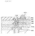
- a core substrate board formed with a lower-layer conductor circuit is coated with an electroless plating adhesive comprising a photosensitive resin and, after the coat is dried, exposure to light and development are carried out to provide an interlayer resin insulating layer having openings for via holes.
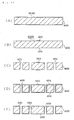
- the surface of this interlayer resin insulating layer is roughened with an oxidizing agent or the like and a thin electroless plated copper layer is formed on said interlayer resin insulating layer.
- a plating resist is disposed thereon and a thick electroplated copper layer is constructed.
- the plating resist is then stripped off and the thin electroless plated copper layer is etched off to provide a conductor circuit pattern including via holes. This procedure is repeated a plurality of times to provide a multilayer printed circuit board.
- the direct-current plating (DC plating) method which is one of the conventional electroplating techniques, is used to provide said electroplated copper layer on a substrate surface
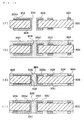
- the current generally tends to be concentrated in the marginal area of the substrate surface as compared with the central area so that, as illustrated in Fig. 6 , the thickness t 12 of the copper layer in the marginal area of the substrate surface tends to become greater than the thickness t 11 in the central area, thus causing a regional variation in thickness of the electroplated copper layer.
- said substrate surface is the surface of a substrate board (work size substrate) having a large area corresponding to a large number of printed circuit boards integrated (specifically, the average one has an area of 255 to 510 mm square and there is even one having an area of about 1020 mm square at a maximum), the above tendency is particularly pronounced.
- the insulation interval t 14 between conductor layers in the marginal region of the substrate board is relatively smaller than the insulation interval t 13 between conductor layers in the central region of the substrate board as shown in Fig. 7 , so that the thickness of the insulating layer 1101b between conductor layers must be increased in order to insure a sufficient insulation in all regions of the printed circuit board but this is a hindrance to the implementation of high-density wiring.
- the crystallinity of the plated copper is low because of the use of an organic additive for improved throwing power.
- the residual stress in the plated copper layer is fairly large so that the layer tends to develop cracks and other flaws and show low elongation and high tensile strength characteristics. Therefore, an annealing step for reducing the residual stress has been essential to the manufacture of printed circuit boards.
- the thick plated copper layer formed by electroless plating is poor in ductility because of the unavoidable contamination of the layer with many impurities inclusive of the additives used. Therefore, when a thick plated copper layer is formed by electroless plating, the reliability for the wiring and connection is insufficient and in order to attain a sufficient degree of reliability, an annealing step is indispensable in this case, too.
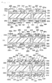
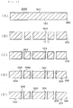
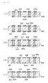
- the constant-current pulse electroplating process is characterized in that the plating current is controlled at a constant level and the representative waveform involved is a square wave.
- This technology may be further divided into the process (PC plating process; Fig. 8 ) in which the current is controlled by means of the square pulse wave available by repetition of the alternating supply (ON) and interruption (OFF) of the cathode current and the pulse-reverse electroplating method (PR plating method; Fig. 9 ) in which the current is controlled with a periodically reversed wave available by repetition of the alternating supply of cathode current and supply of anode current.
- PC plating process Fig. 8
- PR plating method PR plating method
- the non-steady diffusion layer can be reduced in thickness in either process, with the result that a smooth plated metal layer can be constructed and further that since plating can be effected at a high pulse current density (high overvoltage), the evolution of crystal seeds is promoted to yield finer crystal grains, thus enabling formation of a plated metal layer of high crystallinity.
- the PR electroplating method the process disclosed by Fuj inami et al. (Surface Technology, "Formation of Via Filling by PR Electrolysis", 48[6], 1997, p.86-87 ).
- the uniformity of layer thickness is superior to that obtainable by direct current plating process but is not as good as the objective level ( Fig. 4 ).
- the plated copper layer formed by PR process is improved in the uniformity of thickness as compared with the layer obtainable by PC process but is not as high as desired yet and, moreover, plating by PR process requires an expensive current source.
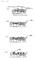
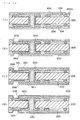
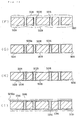
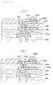
- a copper-clad laminate 3330A comprising a resin substrate 3330 and, as clad to both sides thereof, a copper foil 3331 ( Fig. 27 (A) ) is used.
- through holes 3332 are drilled in this core board ( Fig. 27 (B) ).
- a plating metal is uniformly deposited (3333) to formplated-through holes 3336 in said holes 3332 ( Fig. 27 (C) ).
- the copper foil 3331 formed with the plated metal layer 3333 is subjected to pattern-etching to provide a conductor circuit 3334 ( Fig. 27 (D) ).
- plating is performed to provide a conductor circuit 3358 ( Fig. 27 (E) ).
- the thickness of copper foil 3331 is at least 18 ⁇ m and the thickness of the plated metal layer formed thereon is 15 ⁇ m. Since the combined thickness is as large as 33 ⁇ m, etching produces undercuts on the lateral sides of the conductor 3334 as shown in Fig. 27 (D) and since the circuit layer then is liable to peel off, it has been impossible to construct a fine-line conductor circuit.
- the conductor circuit 3358 on the interlayer resin insulating layer 3350 shown in Fig. 27 (E) , has been formed in a thickness of about 15 ⁇ m.
- the conductor circuit 3334 on the core board 3330 has a thickness of 33 ⁇ m. This means that a large impedance difference is inevitable between the conductor circuit 3358 on the interlayer resin insulating layer 3350 and the conductor circuit 3334 on the core board and because of difficulties in impedance alignment, the high-frequency characteristic of the circuit board cannot be improved.
- the plating metal is deposited in the same thickness over the via hole openings and the conductor circuit-forming area.
- the conventional printed circuit board has the drawback that its size and thickness are increased beyond what are required.
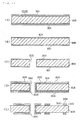
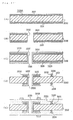
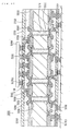
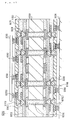
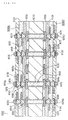
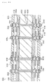
- the printed circuit board 5210 for use as a package board for mounting the IC chip 5290 is fabricated by building up interlayer resin insulating layers 5250, 5350 and conductor layers 5258, 5358 in an alternating manner on a core board 5230 formed with plated-through holes 5236 and disposing bumps 5276U for connection to the IC chip 5290 on the top surface and bumps 5276D for connection to a mother board on the bottom side.
- the electrical connection between the top and bottom conductor layers is afforded by via holes 5260, 5360.
- the via holes 5260 are adjacent to the IC chip 5290 of the core board 5230, the via holes 5360 adjacent to the mother board. These via holes are connected to each other through the corresponding plated-through holes 5236.
- Fig. 38 (B) which is a sectional view taken along the line B-B of Fig. 38 (A)
- the land 5236a of the plated-through hole 5236 is provided with an inner layer pad 5236b for via-hole connection to the upper layer, while the via hole 5260 is connected to this inner layer pad 5236b.
- the package board is formed with a larger number of bumps on the face side than on the reverse side. This is because the wirings from the plurality of bumps on the surface are consolidated and connected to the bumps on the reverse side.
- the power lines required to be of low resistance compared with signal lines, which number 20, for instance, on the face side (IC chip side) are consolidated into a single line on the reverse side (on mother board side).
- the buildup circuit layer formed on the face side of a core board and the buildup circuit layer on the reverse side may be consolidated at the same pace for the purpose of equalizing the number of upper buildup circuit layers to the number of lower buildup circuit layers, that is to say for minimizing the number of layers.
- the wirings are consolidated to some extent in the buildup circuit layer on the face side and then connected to the buildup circuit layer on the reverse side through the plated-through holes in the multilayer core board.
- the number of built-up layers is increased so that the reliability of connection between the upper and lower layers is low.
- the cost of the package board is increased and the size, thickness and weight of the package board are unnecessarily increased.
- the present invention has for its object to provide a multilayer printed circuit board contributory to reduction in the number of layers of the buildup structure and a multilayer printed circuit board contributory to reduction in the internal wiring length.
- the first invention is concerned with an electroless plating solution comprising an aqueous solution containing 0.025 to 0.25 mol/L of a basic compound, 0.03 to 0.15 mol/L of a reducing agent, 0.02 to 0.06 mol/L of copper ion and 0.05 to 0.30 mol/L of tartaric acid or a salt thereof.
- the second invention is concerned with an electroless plating solution comprising an aqueous solution containing a basic compound, a reducing agent, copper ion, tartaric acid or a salt thereof and at least one ion species selected from the group consisting of nickel ion, cobalt ion and iron ion.
- the third invention is concerned with an electroless plating process which comprises immersing a substrate in the electroless plating solution according to either said first invention or said second invention and performing electroless copper plating at a deposition rate set to 1 to 2 ⁇ m/hour.
- the fourth invention is concerned with a process for manufacturing a printed circuit board which comprises immersing a resin insulating substrate board in the electroless plating solution according to either said first invention or said second invention and performing electroless copper plating at a deposition rate set to 1 to 2 ⁇ m/hour to provide a conductor circuit.
- the fifth invention is concerned with a printed circuit board comprising a resin insulating substrate board formed with a roughened surface and, as built thereon, a conductor circuit comprising at least an electroless plated film wherein that said electroless plated film has a stress of 0 to +10 kg/mm 2 .
- the sixth invention is concerned with a printed circuit board comprising a resin insulating substrate board formed with a roughened surface and, as built thereon, a conductor circuit comprising at least an electroless plated film wherein said electroless plated film is complementary to said roughened surface and convex areas of the roughened surface is relatively greater in thickness than said film in concave areas of said roughened surface.
- the seventh invention is concerned with a printed circuit board comprising a substrate board formed with a lower-layer conductor circuit and, as built thereon, an upper-layer conductor circuit through the intermediary of an interlayer resin insulating layer, with said upper-layer conductor circuit and said lower-layer conductor circuit being interconnected by via holes, wherein said upper-layer conductor circuit comprises at least an electroless plated film, said interlayer resin insulating layer is provided with a roughened surface, said electroless plated film is complementary to said roughened surface, and bottoms of said via holes are also provided with an electroless plated film having a thickness equal to 50 to 100% of the thickness of the electroless plated film on said interlayer resin insulating layer.
- the eighth invention is concerned with a printed circuit board comprising a resin insulating substrate board and, as built thereon, a conductor circuit comprising at least an electroless plated film, wherein said electroless plated film comprises copper and at least one metal species selected from the group consisting of nickel, iron and cobalt.
- the thickness of any copper foil, conductor layer or conductor circuit as mentioned in this specification is the mean of thicknesses measured on a light or electron microphotograph of its cross-section.
- An electroplating process for electroplating a conductive substrate surface wherein said electroplating is performed intermittently using said substrate surface as cathode and a plating metal as anode at a constant voltage between said anode and said cathode.
- the intermittent electroplating in the above electroplating process is carried out by repeating application of a voltage between the cathode and anode and interruption thereof in an alternating pattern, and preferably the voltage time/interruption time ratio is 0.01 to 100, the voltage time is not longer than 10 seconds and the interruption time is not shorter than 1x10 -2 seconds.
- a process for producing a circuit board which comprises forming a conductor circuit on a substrate board by electroplating, wherein said electroplating is performed intermittently using the conductive surface on which a conductor circuit is to be formed as cathode and a plating metal as anode at a constant voltage between said anode and said cathode.
- said intermittent electroplating is carried out by repeating application of a voltage between the cathode and anode and interruption thereof in an alternating pattern, and preferably the voltage time/interruption time ratio is 0.01 to 100, the voltage time is not longer than 10 seconds and the interruption time is not shorter than 1x10 -2 seconds.
- the above circuit comprises electrodes and mounting pads in addition to a conductor circuit pattern.
- a process for producing a printed circuit board which comprises disposing a resist on a conductive layer on a substrate board, performing electroplating, stripping the resist off, and etching said conductive layer to provide a conductor circuit, wherein said electroplating is performed intermittently using said conductive layer as cathode and a plating metal as anode at a constant voltage between said anode and said cathode.
- a process for producing a printed circuit board which comprises constructing an interlayer resin insulating layer on a conductor circuit-forming substrate board, forming openings for via holes in said interlayer resin insulating layer, forming an electroless plated metal layer over said interlayer resin insulating layer, disposing a resist thereon, performing electroplating, stripping the resist off and etching the electroless plated metal layer to form a conductor circuit pattern and via holes, wherein said electroplating is performed intermittently using said electroless plated metal layer as cathode and a plating metal as anode at a constant voltage between said anode and said cathode.
- a metal layer may have been formed on the surface of the interlayer resin insulating layer.
- the intermittent electroplating in the above third and fourth inventions comprises application of a voltage between the cathode and anode and interruption thereof in an alternating pattern, and preferably the voltage time/interruption time ratio is 0.01 to 100, the voltage time is not longer than 10 seconds and the interruption time is not shorter than 1x10 -2 seconds.
- the percent elongation of said copper film as a characteristic parameter is preferably not less than 7%.
- a printed circuit board comprising a copper film circuit on a substrate board, wherein said copper film has properties that (a) its crystallinity is such that the half-width of X-ray diffraction of the (331) plane of copper is less than 0. 3 deg. and (b) the variation in thickness of plated metal layer measured over the whole surface of said substrate, i.e. ((maximum thickness-minimum thickness)/average thickness), is not greater than 0.4.
- a printed circuit board comprising an interlayer resin insulating layer on a substrate board for the formation of a conductor circuit and, as disposed on top of said interlayer resin insulating layer, a copper-film conductor circuit, with via holes provided in said interlayer resin insulating layer interconnecting said conductor circuits, wherein said copper film has properties that (a) its crystallinity is such that the half-width of X-ray diffraction of the (331) plane of copper is less than 0.3 deg. and (b) the variation in thickness of said copper film (electroplated copper layer) measured over the whole surface of said substrate, i.e. ((maximum thickness-minimum thickness)/average thickness), is not greater than 0.4.
- the copper film in the above sixth and seventh inventions is preferably further has its percent elongation of not less than 7%.
- the above relates broadly to a technology for fabricating conductor circuits for semiconductor devices and printed circuit boards and an electroplating technology such that intermittent electroplating is performed in a plating metal ion-containing plating solution using the substrate surface as cathode and the plating metal as anode with the voltage between said anode and cathode being kept constant.
- the intermittent electroplating described above insures a uniform plating thickness.
- the thickness of the conductor circuits for circuit boards such as semiconductor devices and printed circuit boards can be rendered uniform. Therefore, not only is impedance alignment facilitated but, because the thickness of the interlayer resin insulating layer is uniform, an improved interlayer insulation is materialized. Furthermore, because of high crystallinity and high elongation characteristics, the residual stress in the plated metal layer is low so that even fine line-definition patterns can be protected against peeling. Therefore, the connection reliability of circuits is improved.
- the above intermittent electroplating process comprises application of a voltage between the cathode and anode and interruption thereof in an alternating pattern, and preferably the voltage time/interruption time ratio is 0.01 to 100, the voltage time is not longer than 10 seconds and the interruption time is not shorter than 1x10 -12 seconds. If the voltage time exceeds 10 seconds, the film thickness will become uneven as it is the case with the conventional direct-current electroplating, and when the interruption time is less than 1x10 -12 seconds, the diffusion of metal ions will be insufficient to detract from crystallinity.
- the optimum voltage time/interruption time ratio is 0.1 to 1.0.
- the electroplating mentioned above is preferably copper plating, nickel plating, cobalt plating, tin plating or gold plating.
- the copper plating solution is preferably an aqueous solution of sulfuric acid and copper sulfate.
- the nickel plating solution may for example be an aqueous solution of nickel sulfate, nickel chloride, and boric acid.
- the cobalt plating solution may be an aqueous solution of cobalt chloride, basic cobalt carbonate and phosphorus acid.
- the tin plating solution may be an aqueous solution of stannous chloride.
- gold plating an aqueous solution of gold chloride, potassium cyanide and gold metal can be used.
- the electroplating bath need not be supplemented with a brightener and other additives, the crystallinity of the plated metal deposit is remarkably high.
- the metal in the form of a ball or a rod, for instance, can be used as the plating metal which serves as the anode.
- the substrate board which can be used includes metal, semiconductor, resin and ceramic substrates, among others.
- the surface of the substrate board is made electrically conductive so that it may be successfully electroplated.
- the technique for imparting electrical conductivity to a resin substrate or a ceramic substrate comprises forming metal layer by using an electroless plated deposit layer or a sputter-metalized layer.
- the technique of incorporating a colloidal or powdery metal in the matrix resin can be used.
- a resist is disposed where necessary.
- the plating metal adheres to the conductive surface not covered with resist but exposed.
- This substrate is immersed in the electroplating solution and subjected to intermittent electroplating using the substrate as cathode and the plating metal as anode.
- the substrate which can be used includes insulating substrates such as a resin substrate and a ceramic substrate.
- the resin substrate mentioned above includes an insulating board prepared by laminating prepregs each comprising a fibrous matrix impregnated with a thermosetting resin, a thermoplastic resin or a thermosetting resin-thermoplastic resin complex or a copper-clad laminate board prepared by laying up such prepregs and copper foils and hot-pressing them.
- glass cloth As the fibrous matrix mentioned above, glass cloth, aramid cloth, etc. can be used.
- An electroless plating catalyst such as a Pd catalyst is applied to the surface of said insulating substrate board to form an electroless plated layer.
- the copper foil as such can be utilized as cathode.
- the plating resist is then disposed thereon.
- the plating resist can be formed by a process which comprises pasting a photosensitive dry film followed by exposure and development or a process which comprises coating the substrate board with a liquid resist followed by exposure and development.
- the conductor circuit is formed by intermittent electroplating using the conductive layer not covered with resist but exposed, e.g. electroless plated metal layer as cathode and the plating metal as anode.
- the plating resist is stripped off and the conductive layer, e.g. electroless plated metal layer, is etched off with an etching solution to complete the conductor circuit.
- the conductive layer e.g. electroless plated metal layer
- an aqueous system of sulfuric acid-hydrogen peroxide, ferric chloride, cupric chloride or ammonium persulfate, for instance, can be used.
- a conductor circuit-forming substrate board is first provided with an interlayer resin insulating layer, which is then formed with openings for via holes.
- the openings are provided by exposure, development or irradiation with laser light.
- thermosetting resin a thermoplastic resin, a partially photosensitized thermosetting resin, or a complex resin comprising thereof can be used.
- the above interlayer resin insulating layer can be formed by coating with an uncured resin or an uncured resin film by pressure bonding under heating.
- an uncured resin film carrying a metal layer, e.g. copper foil, on one side can be bonded.
- a metal layer e.g. copper foil
- the above resin film formed with a metal layer may for example be a copper foil having resin film.
- the layer formed of an adhesive for electroless plating use can be used as the interlayer resin insulating layer mentioned above.
- the optimum adhesive for electroplating use is a dispersion of a cured acid- or oxidizing agent-soluble heat-resistant resin powder in a substantially acid- or oxidizing agent-insoluble uncured heat-resistant resin. This is because upon treatment with an acid or an oxidizing agent, the heat-resistant resin particles are dissolved and removed so that a roughened surface comprising narrow-necked bottle-like anchors can be provided.
- the cured heat-resistant resin powder mentioned above is preferably 1 a heat-resistant resin powder having an average particle diameter of not more than 10 ⁇ m, 2 a block powder available on aggregation of heat-resistant resin particles having an average particle diameter of not more than 2 ⁇ m, 3 a mixture of a heat-resistant resin powder having an average particle diameter of 2 to 10 ⁇ m and a heat-resistant resin powder having an average particle diameter of not more than 2 ⁇ m, 4 a pseudo-particle comprising a heat-resistant resin powder having an average particle diameter of 2 to 10 ⁇ m and at least one of a heat-resistant resin powder and an inorganic powder each having an average particle diameter of not more than 2 ⁇ m as adhered to the surface of the first-mentioned resin powder, 5 a mixture of a heat-resistant resin powder having an average particle diameter of 0.1 to 0.8 ⁇ m and a heat-resistant resin powder having an average particle diameter of over 0.8 ⁇ m to less
- the substantially acid- or oxidizing agent-insoluble heat-resistant resin mentioned above is preferably a "complex resin comprising a thermosetting resin and a thermoplastic resin” or a “complex resin comprising a photosensitive resin and a thermoplastic resin”. This is because while the former is highly heat-resistant, the latter is capable of forming openings for via holes by a photolithographic technique.
- thermosetting resin which can be used as above includes epoxy resin, phenolic resin and polyimide resin.
- the thermosetting groups are acrylated with methacrylic acid or acrylic acid.
- the optimum resin is an acrylated epoxy resin.
- novolac epoxy resins such as phenol novolac resin and cresol novolac resin and dicyclopentadiene-modified alicyclic epoxy resin.
- thermoplastic resin there can be used polyethersulfone (PES), polysulfone (PSF), polyphenylenesulfone (PPS), polyphenylene sulfide (PPES), polyphenyl ether (PPE), polyetherimide (PI) and fluororesin.
- PES polyethersulfone
- PPS polysulfone
- PPS polyphenylenesulfone
- PPES polyphenylene sulfide
- PPE polyphenyl ether
- PI polyetherimide
- fluororesin fluororesin.
- thermosetting resin photosensitive resin
- thermoplastic resin i.e. thermosetting (photosensitive) resin/thermoplastic resin
- the blending weight ratio of said heat-resistant resin powder is preferably 5 to 50 weight % based on the solid matter of the heat-resistant resin matrix.
- the more preferable ratio is 10 to 40 weight %.
- the heat-resistant resin powder is preferably an amino resin (melamine resin, urea resin, guanamine resin) or an epoxy resin, for instance.
- an electroless plated metal layer is formed over said interlayer resin insulating layer (on the copper foil when a resin-containing copper foil is used) inclusive of surface of openings and after placement of a resist, electroplating is performed to provide a conductor circuit and via holes.
- the electroplating is performed intermittently using said electroless plated metal layer as cathode and the plating metal as anode with the voltage between the anode and cathode being kept constant.
- the resist is stripped off and the electroless plated metal layer is etched off.
- the circuit board and printed circuit board formed by the electroplating process in which the conductor wiring or conductor circuit is made of copper, should satisfy the following conditions (a) and (b).
- the percent elongation mentioned above for the copper layer is preferably not less than 7%. If the elongation is less than 7%, cracks are liable to develop on cold thermal shock.
- the purity of copper deposited is as high as 99.8% or more. Therefore, the inherent ductility of copper is fully expressed to provide a high elongation rate.
- the circuit board mentioned above includes printed circuit boards, IC chips and semiconductor devices such as LSI.
- the first invention is concerned with an electroless plating solution comprising an aqueous solution containing 0.025 to 0.25 mol/L of a basic compound, 0.03 to 0.15 mol/L of a reducing agent, 0.02 to 0.06 mol/L of copper ion and 0.05 to 0.30 mol/L of tartaric acid or a salt thereof.
- the second invention is concerned with an electroless plating solution comprising an alkaline compound, a reducing agent, copper ion, tartaric acid or a salt thereof and at least one metal ion species selected from the group consisting of nickel ion, cobalt ion and iron ion.
- the preferred specific gravity of the electroless plating solutions according to the above first and second inventions is 1.02 to 1.10.
- the preferred temperature of those electroless plating solutions is 25 to 40°C.
- the copper deposition rate of those electroless plating solutions is preferably 1 to 2 ⁇ m/hour.
- the third invention is concerned with an electroless plating process which comprises immersing a substrate in the electroless plating solution of said first or second invention and performing electroless copper plating with the deposition rate set to 1 to 2 ⁇ m/hour.
- said substrate is preferably provided with a roughened surface in advance.
- the fourth invention is concerned with a process for manufacturing a printed circuit board comprising immersing a resin insulating substrate board in the electroless plating solution of said first or second invention and performing electroless copper plating with the deposition rate set to 1 to 2 ⁇ m/hour to provide a conductor circuit.
- the fifth invention is concerned with a printed circuit board comprising a resin insulating substrate board having a roughened surface and, as electroless plated layer thereon, a conductor circuit, wherein said electroless plated layer has a stress value of 0 to +10 kg/mm 2 .
- the sixth invention is concerned with a printed circuit board comprising a resin insulating substrate board having a roughened surface and, as an electroless plated layer thereon, a conductor circuit, wherein said electroless plated layer is complementary to said roughened surface and relatively increased in thickness in convex areas of the roughened surface as compared with concave areas of said surface.
- concave and convex areas mentioned above mean the concave and convex parts of the primary anchor and do not refer to the secondary anchor formed on the convex part thereof or the like (ref. Fig. 16 ).
- the seventh invention is concerned with a printed circuit board which comprises a substrate board formed with a lower conductor circuit, an interlayer resin insulating layer thereon and an upper conductor circuit as built up with said lower conductor circuit connected to said upper conductor circuit through via holes, wherein said upper-layer conductor circuit comprises at least an electroless plated metal film, said interlayer resin insulating layer has a roughened surface, said electroless plated metal film is complementary to said roughened surface throughout and the bottom parts of said via holes are also provided with a electroless plated layer in a thickness equal to 50 to 100% of the electroless plated layer formed on said interlayer resin insulating layer.
- the eighth invention is concerned with a printed circuit board comprising a resin insulating substrate board and as built thereon a conductor circuit comprising at least an electroless plated metal layer, wherein said electroless plated metal layer comprises copper and at least one metal selected from the group consisting of nickel, iron and cobalt.
- the preferred content of said at least one metal selected from nickel, iron and cobalt is 0.1 to 0.5 weight %.
- the electroless plating solution according to the first invention comprises an aqueous solution containing 0.025 to 0.25 mol/L of a basic compound, 0.03 to 0.15 mol/L of a reducing agent, 0.02 to 0.06 mol/L of copper ion and 0.05 to 0.3 mol/L of tartaric acid or a salt thereof.
- the electroless plating solution according to the second invention comprises an aqueous solution containing a basic compound, a reducing agent, copper ion, tartaric acid or a salt thereof and at least one ion species selected from the group consisting of nickel ion, cobalt ion and iron ion.
- the deposition rate of the plating solution can be reduced to 1 to 2 ⁇ m/hr. Therefore, when a plating metal is deposited in the openings for via holes, the copper ions are allowed to diffuse far enough down the openings for via holes so that a sufficiently thick plated metal film can be formed even within fine via holes.
- the electroless plating solution according to the above second invention contains at least one metal ion species selected from the group consisting of nickel ion, cobalt ion and iron ion in addition to tartaric acid or a salt thereof, the evolution of hydrogen is suppressed with the result that an appropriate tensile stress is generated in the plated metal layer to insure a good adhesion to the substrate and, hence, exfoliation of the plated metal from the substrate is hard to take place.
- the specific gravity of those electroless plating solutions is preferably adjusted to 1.02 to 1.10. This is because a plating metal can then be precipitated in the fine openings for via holes.
- the preferred temperature of those electroless plating solutions is 25 to 40°C. If the temperature is excessively high, the deposition will be accelerated so much that the plating metal can hardly be deposited within fine openings for via holes. If the temprature is less than 25°C, it takes so much time to deposit the plated metal layer, therefor the temperature is not practical.
- the above electroless plating solutions preferably contain 0.01 to 0.05 weight % of nickel ion, iron ion and/or cobalt ion.
- the concentration of said at least one: metal ion species selected from the group consisting of nickel, iron and cobalt ions can be controlled within the range of 0.1 to 0.5 weight % to thereby provide a plated metal film which is hard enough and shows good adhesion to the resin insulating layer.
- said basic compound may for example be sodium hydroxide, potassium hydroxide or ammonia.
- the reducing agent mentioned above includes formaldehyde, sodium hypophosphite, NaBH 4 and hydrazine.
- the compound mentioned above as a copper ion includes copper sulfate and copper chloride.
- the above-mentioned salt of tartaric acid includes the corresponding sodium salt and potassium salt and any of those salts may be the salt derived by substituting only one of the available two carboxyl groups with the above-mentioned particular metal or the salt derived by substituting both the carboxyl groups with the above-mentioned metal.
- the compound for providing said nickel ion includes nickel chloride and nickel sulfate; the compound for providing said cobalt ion includes cobalt chloride; and the compound providing for said iron ion includes iron chloride.
- the third invention is concerned with an electroless plating process which comprises immersing a substrate in said electroless plating solution and performing copper electroless plating at the deposition rate set to 1 to 2 ⁇ m/hr as mentioned above.
- the fourth invention is concerned with a process for manufacturing a printed circuit board which comprises immersing a resin insulating substrate board in said electroless plating solution and performing copper electroless plating by the above-mentioned electroless copper plating process to provide a conductor circuit.
- the resin insulating substrate board mentioned above means not only a resin insulating substrate board not formed with a conductor circuit but a resin insulating substrate board formed with a conductor circuit and, in superimposition, further with an interlayer resin insulating layer having openings for via holes.
- the surface of resin insulating layer constituting said substrate and the resin insulating substrate is preferably a roughened surface.
- the roughened surface mentioned above comprises concave areas and convex areas and the plating metal is deposited tracing those concave and convex areas but the thickness of the deposit is larger in the convex areas of the roughened surface than in the concave areas thereof and this thickness profile offers the following advantages.
- the process generally called the semi-additive process which comprises disposing a plating resist on an electroless plated metal layer, performing electroplating to form a thick plated metal film, stripping off said plating resist and etching the electroless plated metal layer beneath the plating resist, the etching operation is easier when the thichness of the electroless plated metal film is relatively thin in the concave areas as compared with the convex areas and the whole plated metal deposit can be easily removed by this etching without leaving unetched areas, with the result that the insulation reliability of the resulting circuit is very satisfactory.
- the printed circuit board fabricated by the process for manufacturing a printed circuit board according to the fourth invention has the following characteristics.
- the printed circuit board according to the fifth invention comprises a resin insulating substrate board having a roughened surface and as built thereon a conductor circuit comprising at least an electroless plated metal film, wherein said electroless plated metal film has a stress value of 0 to +10 kg/mm 2 .
- the sign of the above stress value is positive, i.e. +, which means that a tensile stress has been generated in the above-mentioned plated metal film.
- This stress can be measured with a spiral stress meter (manufactured by Yamamoto Plating Co., Ltd.).
- the plated metal film does not undergo blistering or peeling so that the connection reliability of the conductor circuits is high.
- the printed circuit board according to the sixth invention is a printed circuit board comprising a resin insulating substrate board formed with a roughened surface and as built thereon a conductor circuit comprising at least an electroless plated metal film, wherein said electroless plated metal film is complementary to said roughened surface and the thickness of said electroless plated metal film is relatively thick in the convex areas of the roughened surface compared with the concave areas thereof (that is to say, the electroless plated metal film in the concave areas is relatively thin as compared with the convex areas thereof) .
- the electroless plated metal film in the concave areas of said roughened surface which is thinner than that in the convex areas, can be more readily and completely stripped off, with the result that the problem of unetched residues is obviated in the etching step and a high inter-conductor insulation dependability is assured.
- the printed circuit board according to the seventh invention is concerned with a circuit board which comprises a substrate board carrying a lower conductor circuit built thereon, an interlayer resin insulating layer and an upper conductor circuit as built up with said lower conductor circuit and upper conductor circuit being interconnected by via holes, wherein said upper conductor circuit comprises at least electroless plated metal film, said interlayer resin insulating layer has a roughened surface, said electroless plated metal film is complementary to said roughened surface, and bottoms of said via holes also carry the electroless plated metal film in a thickness equal to 50 to 100% of the thickness of the electroless plated metal film on said interlayer resin insulating layer.
- the above printed circuit board is fabricated using the above-described electroless plating solution and, therefore, via holes can be provided because, even when the openings for via holes are as fine as 80 ⁇ m or less in diameter, a sufficiently thick plated metal film can be formed on the hole bottoms.
- the printed circuit board according to the eighth invention comprises a resin insulating substrate board and, as built thereon, a conductor circuit comprising at least an electroless plated metal film, wherein said electroless plated metal film comprises copper and at least one metal species selected from the group consisting of nickel, iron and cobalt.
- addition of a salt of such a metal ion inhibits the uptake of hydrogen into the plated metal to reduce the compressive stress of plating so that the resulting film may have an improved adhesion to the resin insulating layer. Furthermore, those metals form alloys with copper to increase the hardness of the plated metal film, thus contributing further to the adhesion to the resin insulating layer.
- An electrodeposition layer which is high in hardness and adhesion to the resin insulating layer can be obtained when the content of said at least one metal species selected from among nickel, iron and cobalt is within the range of 0.1 to 0.5 weight %.
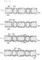
- a process for manufacturing a multilayer printed circuit board comprising at least the following steps (1) to (5).
- a process for manufacturing a multilayer printed circuit board comprising at least the following steps (1) through (7).
- the step of piercing through holes in said copper-clad laminate can be carried out using a laser or a drill.
- the thickness of copper foil is reduced preferably to 1 to 10 ⁇ m, more preferably 2 to 7 ⁇ m.
- a multilayer printed circuit board comprising a core board having a conductor circuit and, as disposed on said conductor circuit, a buildup wiring layers obtainable by building up an interlayer resin insulating layer and a conductor layer alternately, with via holes interconnecting the conductor layers, which has technical properties that the thickness of the conductor circuit on the core board is restricted to a maximum of 10 ⁇ m over the thickness of the conductor layer on the than 7 ⁇ m.
- the thickness of the conductor circuit on said core board is not greater by more that said core board comprises a copper-clad laminate and that the conductor circuit on the core board comprises the copper foil of said copper laminate and a plated metal layer.
- a process for manufacturing a multilayer printed circuit board which comprises thinning the copper foil of a copper-clad laminate by etching, pattern-etching the copper foil of said copper-clad laminate board to form a conductor circuit, and building up an interlayer resin insulating layer and a conductor layer in an alternate fashion over said conductor circuit, wherein the thickness of the conductor circuit on said core board is restricted to a maximum of 10 ⁇ m in excess over the thickness of the conductor layer on the interlayer resin insulating layer.
- the thickness of the copper foil of a copper-clad laminate is reduced by etching. Then, plating is performed to form plated-through holes. In this step, a plated metal film is formed on the copper foil. The copper foil carrying this plated metal film is pattern-etched to construct a conductor circuit. Since the copper foil has been reduced in thickness in advance, the combined thickness of the copper foil and plated metal film to constitute a conductor circuit is small so that a fine-line circuit can be formed by pattern etching.
- the combined thickness of the copper foil and plated metal film forming said conductor circuit will not be small and much different from the thickness of the conductor layer on the interlayer resin insulating layer so that an impedance alignment can be obtained between said conductor circuit on core board and the conductor layer on the interlayer resin insulating layer.
- high-frequency characteristic of the multilayer printed circuit board can be improved.
- a multilayer printed circuit board which comprises thinning the copper foil of a copper-clad laminate by etching, forming a uniform conductor film thereon, plating the resist-free area to construct a conductor circuit, stripping the resist off and etching the conductor film and copper foil under the resist, the copper foil is thinned by etching in the first place so that the combined thickness of conductor film and copper foil is reduced, contributing to the implementation of an elaborate circuit pattern.
- controlling the thickness of the copper foil within the range of 1 to 10 ⁇ m leads to a reduced combined thickness of the copper foil and plated metal film constituting the conductor circuit so that an elaborate circuit can be formed by pattern etching.
- the differential in thickness between the conductor circuit on core board and the conductor layer on the interlayer resin insulating layer can be set small, the impedances of both layers can be easily aligned.
- the optimum copper foil thickness is 2 to 7 ⁇ m.
- a resin filler is filled in between the conductor circuits formed on the surface of a core board so as to prepare a flat surface and, then, an interlayer resin insulating layer is formed thereon but, in accordance with this invention, the interlayer resin insulating layer naturally assumes a flat surface in sole dependence on the inherent levelling function of the interlayer resin insulating layer.
- the core board may have been provided with plated-through holes.
- the difference between the thickness of the plated-through hole conductor and the thickness of the conductor circuit on the interlayer resin insulating layer is so small that an impedance alignment between the two conductors can be more easily attained.
- the thickness of the conductor circuit on the core board is restricted to a maximum of 10 ⁇ m in excess of the thickness of the conductor layer on the interlayer resin insulating layer. Since the thickness of the former is not much different from and the conductor layer on the interlayer resin insulating layer, an impedance alignment can be easily attained between the conductor circuit on the core board and the conductor layer on the interlayer resin insulating layer, with the result that the high-frequency characteristic of the multilayer printed circuit board can be improved.
- the thickness of the conductor circuit on the core board be not greater than the conductor layer on the interlayer resin insulator layer by more than 7 ⁇ m. If the thickness difference between the conductor circuit on the core board and the conductor layer on the interlayer resin insulating layer is too large, a heat cycle-associated stress may develop to cause cracks in the interlayer resin insulating layer.
- the process for manufacturing a multilayer printed circuit board comprises thinning the copper foil of a copper-clad laminate by etching, pattern-etching the copper foil of the copper-clad laminate to provide a conductor circuit, and, over this conductor circuit, building up an interlayer resin insulating layer and a conductor layer alternately and repeatedly to provide a multilayer printed circuit board, wherein the thickness of the conductor circuit on said core board is restricted to a maximum of 10 ⁇ m over the thickness of the conductor layer on the interlayer resin insulating layer.
- Japanese Kokai Publication Hei-2-22887 discloses a process for manufacturing a thin copper-clad substrate board by a 25 to 90% etch of copper foil but this publication does not describe, or even suggest, the manufacture of a multilayer printed circuit board having a multilayer or structure, nor does it address to a problem of an impedance alignment between the conductor circuit on a core board and a conductor layer on an interlayer resin insulating layer, which is mentioned herein, thus differentiating itself from this.
- the copper-clad laminate includes various prepregs such as a glass cloth-epoxy resin prepreg, a glass cloth-bismaleimide-triazine resin prepreg, a glass cloth-fluororesin prepreg or the like, each claded with copper foil.
- a glass cloth-epoxy resin prepreg a glass cloth-bismaleimide-triazine resin prepreg, a glass cloth-fluororesin prepreg or the like
- the copper-clad laminate board both a two-side copper-clad laminate and a one-side copper-clad laminate can be used and a two-side copper-clad laminate is most preferred.
- Adjustment of the thickness of copper foil is effected by etching.
- the specific technique which can be used includes chemical etching with an aqueous sulfuric acid-hydrogen peroxide solution or an aqueous solution of ammoniumpersulfate, cupric chloride or ferric chloride or physical etching such as ion beam etching.
- the etching rate is preferably 0.001 to 10 ⁇ m/min., particularly 0.01 to 0.3 ⁇ m/min. If the etching rate is too fast, thickness control will be difficult and a variation in thickness will be large. Conversely, an excessively slow etching speed will not be practically acceptable.
- the etching temperature is preferably 20 to 80°C.
- the etching can be effected by whichever of spraying and dipping.
- the optimum variation in the etch-reduced thickness of copper foil is not greater than ⁇ 1.0.
- the thickness of said copper-clad laminate is preferably 0.5 to 1.0 mm. If the laminate is too thick, it cannot be neatly pierced, and if it is too thin, warpage tends to take place.
- the laser for use in the formation of through holes is preferably a short-pulse carbon dioxide laser with an output of 20 to 40 mJ and a pulse duration of 10 -4 to 10 -8 seconds.
- the number of shots may be 5 to 100 shots.
- a filler may be filled into the plated-through holes.
- the metallized inner walls of plated-through holes may be roughened.
- the thickness of the copper foil and the metal layer is preferably 10 to 30 ⁇ m.
- fillers comprising bisphenol F epoxy resin and inorganic particulate fillers such as silica, alumina, etc., and those comprising particulate metal and particulate resin and the like can be used.
- the substrate board thus formed with plated-through holes is then provided with a conductor circuit.
- the conductor circuit is formed by an etching technique.
- the surface of the conductor circuit is preferably roughened for improved adhesion.
- an interlayer resin insulating layer comprising insulating resin is constructed.
- the interlayer resin insulating layer may comprise an adhesive for electroless plating use.
- the surface of the insulating resin layer can be roughened by, for example, incorporating a powder soluble in an acid or oxidizing agent in the heat-resistant resin in advance which is hardly soluble in the acid or oxidizing agent and dissolving the powder with the acid or oxidizing agent.
- the heat-resistant resin powder mentioned above includes powders of various amino resins (melamine resin, urea resin, guanamine resin, etc.), epoxy resins (the optimum resin is a bisphenol epoxy resin cured with an amine series curing agent), bismaleimide-triazine resin and other heat-resistant resins.
- such an adhesive for electroless plating use may be supplemented with a cured heat-resistant resin powder, an inorganic powder and/or a fibrous filler.
- the heat-resistant resin powder mentioned above is preferably at least one member selected from the group consisting of (1) a heat-resistant resin powder having an average particle diameter of not more than 10 ⁇ m, (2) a flocculated particle derived from heat-resistant resin particles having an average diameter of not more than 2 ⁇ m, (3) a mixture of a heat-resistant resin powder having an average particle diameter of 2 to 10 ⁇ m and a heat-resistant resin powder having an average particle diameter of less than 2 ⁇ m, (4) a pseudo-powder comprising a heat-resistant resin powder having an average diameter of 2 to 10 ⁇ m and, as adhered to the surface thereon, at least one member selected from the group consisting of a heat-resistant resin powder or inorganic powder having an average particle diameter of not more than 2 ⁇ m, (5) a mixture of a heat-resistant resin powder having an average particle diameter of more than 0.8 ⁇ m but less than 2.0 ⁇ m and a heat-resistant resin powder having an average particle diameter of 0.1 to 0.8 ⁇ m and (6)
- the interlayer resin insulating layer can be formed with openings by means of a laser beam or by actinic light exposure and development.
- a catalyst for electroless plating use such as a Pd catalyst, is applied and the interior of the openings for via holes is plated to form the required via holes and, in addition, a conductor circuit is formed on the surface of the insulating resin layer.
- a plating resist is disposed and electroplating is carried out, the plating resist is then stripped off and a conductor circuit is formed by etching.
- a technology for manufacturing a multilayer printed circuit board which comprises forming an interlayer insulating layer on a substrate board carrying a bottom-layer conductor circuit, piercing openings in said interlayer insulating layer, imparting electrical conductivity to the surface of said interlayer insulating layer and inner walls of openings, filling up the openings by electroplating to provide via holes, and then forming an upper-layer conductor circuit, wherein said electroplating is performed using a plating solution comprising an aqueous solution containing 0.1 to 1.5 mmol/L of at least one additive selected from the group consisting of a thiourea, a cyanide and a polyalkylene oxide and a metal ion species.
- an aqueous solution containing 0.1 to 1.5 mmol/L of at least one additive selected from the group consisting of thioureas, cyanides and polyalkylene oxides and a metal ion species is used as the electroplating solution.
- the above-mentioned additive for incorporation in the electroplating solution is by nature ready to be adsorbed on the surface of conductive substances such as metals. Therefore, the additive is deposited on the surface of the interlayer insulating layer and the inner walls of the openings, which have been made conductive in advance.
- the rate of deposition of said additive depends on the rate of diffusion, the deposition does not take place at a uniform rate but rather the additive is adhered to more readily on the conductivity-imparted surface of the interlayer insulating layer (the lands of via holes and the wiring), not adsorbing into the openings.
- the deposited additive acts as a plating inhibitor to interfere with the deposition by electroplating. Therefore, the metal ion is preferentially precipitated in the openings for via holes in the course of electroplating, while the ion is harder to be deposited on the conductivity-imparted surface of the insulating layer. As a result, whereas the interiors of openings for via holes are filled up with the metal deposit, the thickness of the conductor circuit-forming metal film on the surface of the insulating layer is not increased as much. Thus, the filling of openings for via holes with the plating metal and the formation of a circuit board are concurrently achieved.
- At least one member selected from the group consisting of thioureas, cyanides and polyalkylene oxides can be employed.
- the thiourea mentioned above is preferably at least one compound selected from the group consisting of thiocarbamide (which is also known generally as thiourea) and isothiourea.
- the cyanide mentioned above is preferably an alkali metal cyanide.
- the alkali metal cyanide includes sodium cyanide and potassium cyanide.
- the preferred species of said polyalkylene oxide is polyethylene glycol.
- additives can be used each independently or in a combination of two or more species.
- the concentration of said additive is 0.1 to 1.5 mmol/L.
- the additive will not be deposited on the inner walls of openings for via holes at all so that the metal ion precipitates out in excess in the interior of the openings for via holes causing an excess blister of the deposited metal from the openings, while the metal ion will not precipitate appreciably on the conductor circuit. If the amount of the additive exceeds 1.5 mmol/L, the additive will be deposited as much on the interior of openings for via holes as on the conductivity-imparted surface of the insulating layer, with the result that the openings cannot be filled up with the plating metal.
- a thiourea is used as the additive, its concentration is preferably 0.3 to 0.5 mmol/L, for in this range the openings for via holes will present with a flat smooth surface.
- the metal ion species to be incorporated in the electroplating solution for use in this invention of the fourth group includes copper ion, nickel ion, cobalt ion, tin ion and gold ion.
- an aqueous solution containing copper sulfate and sulfuric acid is preferably used.
- the preferred nickel plating solution is an aqueous solution containing either nickel sulfate or nickel chloride and boric acid.
- the cobalt plating solution is preferably an aqueous solution containing either cobalt chloride or basic cobalt carbonate and hypophosphorous acid.
- the tin plating solution is preferably an aqueous solution of tin chloride.
- the gold plating solution is preferably an aqueous solution containing gold chloride or gold-potassium cyanide.
- the electroplating solution mentioned above may be thickened by adding glycerin, polyethylene glycol, cellulose, chitosan or the like. Thickening results in retarded diffusion of the additive so that a definite difference can be easily established in the deposition amount of the additive between the opening for a vial hole and the surface of the insulating layer and, hence, it is easier to fill up the openings for via holes with the plating metal.
- the filling of via holes and the formation of a conductor circuit can be concurrently accomplished by using at least one additive selected from the group consisting of thiourea, cyanides and polyalkylene oxides as a plating inhibitor.
- Japanese Kokai Publication Sho-57-116799 discloses a technology wherein electroplating and acid cleaning are performed in a thiourea-containing aqueous solution of sulfuric acid.
- Japanese Patent Publication Sho-62-8514 discloses a technology for pattern plating with a thiourea-containing copper sulfate plating solution.
- Japanese Kokai Publication Sho-49-3833 discloses a process for manufacturing a multilayer circuit board wherein a selective electroless plating is performed with thiourea.
- the process comprises constructing an interlayer insulating layer on a bottom-layer conductor circuit-carrying substrate board, piercing openings in this interlayer insulating layer, imparting electrical conductivity to the surface of said interlayer insulating layer and inner walls of said openings and finally performing electroplating.
- the preferred opening for a vial hole with which the interlayer insulating layer is to be provided has an aspect ratio, i.e. the depth/diameter of the opening, of 1/3 to 1/1. If the aspect ratio is less than 1/3, the opening will be too large in diameter to fill up with the plating metal. On the other hand, if the aspect ratio exceeds 1/1, the metal ions will be hard to diffuse into the openings, resulting in a failure to fill up with the plating metal.
- the diameter of openings for via holes is preferably 20 to 100 ⁇ m. This because if 100 ⁇ m is exceeded, the metal ion may not be supplied in a sufficient amount to fill the via holes. Conversely, if the diameter is less than 20 ⁇ m, the metal ion will not be able to diffuse well into the via holes, thus failing to fill the holes.
- the depth of the openings for via holes is preferably 10 to 100 ⁇ m. If the depth is less than 10 ⁇ m, the interlayer insulation will be too thin. If it exceeds 100 ⁇ m, the metal ions will not easily diffuse and those may not be supplied in a sufficient amount to fill up with the plating metal.
- the means for imparting electrical conductivity to the surface of said interlayer insulating layer and the inner walls of openings includes the formation of a metal layer by electroless plating, sputtering or vapor deposition.
- the metal layer mentioned above is preferably comprised of at least one member selected from the group consisting of copper, nickel, tin and noble metals.
- the thickness of said metal layer is preferably 0.1 to 1.0 ⁇ m. If the thickness is less than 0.1 ⁇ m, electroplating may not be successfully accomplished. If 1 ⁇ m is exceeded, there will be cases in which the deposited metal cannot be etched off to provide a discrete conductor circuit.
- the plating metal as anode may be in the form of a ball or a rod, for instance.
- the current density is preferably 0.5 to 3 A/dm 2 .
- the rationale is that at a current density of less than 0.5 A/dm 2 , the effect of the additive contained in the plating solution will be too weak to successfully fill the via holes. If, conversely, the current density exceeds 3A/dm 2 , the supply of the metal ion will not catch up with the deposition speed to cause an uneven electrodeposition, leading to the so-called "burnt plating".
- the thickness of the conductor circuit after electroplating is preferably 5 to 30 ⁇ m. If the conductor circuit is less than 5 ⁇ m in thickness, the etch-off of the thin conductivity-imparting layer formed for electroplating may result in elimination of the very conductor circuit formed. In order to form a conductor circuit over 30 ⁇ m in thickness, the thickness of the plating resist must be increased, with the result that a fine conductor circuit pattern cannot be implemented.
- intermittent electroplating can be formed in a plating solution containing the plating metal ion using the conductor circuit-forming surface (substrate surface) as cathode and the plating metal as anode to provide a thick conductor circuit.
- the constant-voltage pulse plating mentioned above is outstanding in the uniformity of deposited film thickness and, therefore, makes it possible to provide conductor circuits of uniform thickness capable of impedance alignment in the final multilayer printed circuit board.
- the reason why the uniformity of plating thickness can be attained by said intermittent electroplating is that at the edges of the substrate surface and in the vicinity of openings for via holes, where the amount of electrodeposition tends to be large, the metal deposit is melted by the spike current flowing momentarily toward the anode and, conversely, in the center of the substrate surface and within the openings for via holes, where the amount of electrodeposition tends to be smaller, the plating metal is caused to precipitate out by the spike current flowing momentarily toward the cathode just as in the remaining area, with the result that a highly uniform electrodeposition can be achieved.
- the reason why said intermittent electroplating results in an increased crystallinity of the plated metal film is that every interruption of voltage application causes a diffusion of the metal ion near the interface of the surface being plated to insure a constant ion concentration so that a defect of the crystal lattice hardly occurs in the electrodeposited metal film.
- a multilayer printed circuit board which comprises a buildup circuit stratum obtainable by building up interlayer resin insulating layers and conductor layers alternately, with said conductor layers being interconnected by via holes, as constructed on both sides of a core board, wherein said via holes are formed to plug the through holes in the plated-through holes of said core board.
- the through holes in said plated-through holes are preferably not larger than 200 ⁇ m in diameter.
- a process for manufacturing a multilayer printed circuit board comprising at least the following steps (1) to (4).
- via holes are formed in the manner of filling the through holes in the plated-through holes formed in the core board and as the region immediately over the plated-through hole is thus allowed to function as an internal layer pad, the dead space is eliminated. Moreover, since there is no need for wiring the internal layer pad for the connection from the plated-through hole to the via hole, the land configuration of the plated-through hole can be true-round.
- the layout density of plated-through holes in the multilayer core board can be increased, and because the wires can be consolidated at the same pace between the multilayer circuit stratum formed on the face side of the core board and the multilayer circuit stratum formed on the reverse side, the number of layers can be minimized by equating the number of layers of the upper-layer multilayer circuit stratum to the number of layers of the lower-layer multilayer circuit stratum. Furthermore, since the via hole is disposed immediately over the plated-through hole, the wiring length can be decreased to increase the signal transmission speed.
- the through hole in the plated-through hole is not larger than 200 ⁇ m in diameter, formation of a via hole in the manner of filling the through hole does not result in any remarkable increase in the size of the via hole so that the wiring density in the interlayer resin insulating layer provided with via holes is not decreased.
- An adhesive for electroless plating is preferably used as said interlayer resin insulating layer.
- the optimum electroless plating adhesive is a dispersion of a cured heat-resistant resin powder soluble in an acid or an oxidizing agent in an uncured heat-resistant resin which is hardly soluble in the acid or oxidizing agent.
- the heat-resistant resin powder Upon treatment with the acid or oxidizing agent, the heat-resistant resin powder is dissolved and removed to leave a roughened surface which comprises anchors resembling narrow-neck pots.
- said electroless plating adhesive particularly in regard of said cured heat-resistant resin powder, the same kinds of adhesives as mentioned before for the inventions of the first group can be used. This is because, with those adhesives, the more complex anchors can be produced.
- Rmax 0.01 to 20 ⁇ m for insuring a good adhesion to the conductor circuit.
- the range of 0.1 to 5 ⁇ m is preferred because the electroless plated metal film can then be removed without sacrificing the adhesion.
- the heat-resistant resin which is hardly soluble in an acid or an oxidizing agent, mentioned above, is preferably "a complex resin comprising a thermosetting resin and a thermoplastic resin” or "a complex resin comprising a photosensitive resin and a thermoplastic resin".
- the former is excellent in heat resistance, while the latter enables photolithographic formation of openings for via holes.
- thermosetting resin is the same resin as mentioned hereinbefore.
- thermoplastic resin can be the same resin as mentioned hereinbefore.
- the weight ratio of the above heat-resistant resin powder to the solid matter of said heat-resistant resin matrix is preferably 5 to 50 weight %, more preferably 10 to 40 weight %.
- the heat-resistant resin powder is preferably of the same type as that mentioned be for.
- the adhesive layer may be comprised of two layers each having a different composition.
- solder resist layer added to the surface of the multilayer printed circuit board a variety of resins can be used.
- resins can be used.
- bisphenol A epoxy resin, bisphenol A epoxy resin acrylate, novolac epoxy resin, and novolac epoxy resin acrylate cured with an amine series curing agent or an imidazole series curing agent can be mentioned.
- solder resist layer is made of a resin having a rigid skeleton, the layer tends to peel off. Such peeling of the solder resist layer can be prevented by providing a reinforcing layer.
- the epoxy resin obtainable by reacting a phenol novolac or cresol novolac glycidyl ether with acrylic acid or methacrylic acid, for instance, can be used.
- the imidazole series curing agent mentioned above is preferably liquid at 25°C. Being a liquid, it can be uniformly blended.
- the liquid imidazole series curing agent includes 1-benzyl-2-methylimidazole (product designation: IB2MZ), 1-cyanoethyl-2-ethyl-4-methylimidazole (product designation: 2E4MZ-CN), and 4-methyl-2-ethylimidazole (product designation: 2E4MZ).
- the amount of addition of said imidazole series curing agent is preferably 1 to 10 weight % based on the total solid matter of said solder resist composition. This is because, within the above range, uniform blending can be effected.
- a glycol ether series solvent as a solvent is preferably used.
- the solder resist layer formed from such a composition does not generate free acids so that the copper pad surface is not oxidized. Moreover, the risk for health hazards is low.
- glycol ether series solvent mentioned above is used preferably in a proportion of 10 to 70 wt. % based on the total weight of the solder resist composition.
- solder resist composition described above may be supplemented with various antifoams, leveling agents, thermosetting resins for improving heat resistance and alkali resistance or imparting flexibility, and/or photosensitive monomers for improving image resolution.
- the preferred leveling agent is an acrylic ester polymer.
- the preferred initiator includes Ciba-Geigey's Irgacure 1907, and the preferred photosensitizer includes Nippon Kayaku's DETX-S.
- the solder resist composition may be further supplemented with a dye or pigment. This is because the wiring pattern can be masked. As such a dye, phthalocyanine blue is preferred.
- the thermosetting resin mentioned above as an additive includes bisphenol epoxy resin.
- the bisphenol epoxy resin includes bisphenol A epoxy resin and bisphenol F epoxy resin.
- the former is preferred when alkali resistance is an important parameter, while the latter is preferred when viscosity reduction is required (when coatability is an important consideration).
- the photosensitive monomer mentioned above as an additive component includes polyfunctional acrylic monomers. This is because such polyfunctional acrylic monomers contribute to improving image resolution.
- polyfunctional acrylic monomers Nippon Kayaku's DPE-6A and Kyoeisha Kagaku's R-604 can be mentioned by way of example.
- the viscosity of such a solder resist composition is preferably 0.5 to 10 Pa ⁇ s at 25°C, more preferably 1 to 10 Pa ⁇ s. Within this viscosity range, the composition can be easily applied with a roll coater.
- a multilayer printed circuit board comprising a buildup wiring layers obtainable by building up an interlayer resin insulating layer and a conductor layer alternately, with each conductor layers being interconnected by via holes, as constructed on both sides of a core board, wherein lower-layer via holes are disposed immediately over the plated-through holes formed in said core substrate, with upper-layer via holes being disposed immediately over said lower-layer via holes.
- a multilayer printed circuit board comprising buildup wiring statum obtainable by building up an interlayer resin insulating layer and a conductor layer alternately, with each conductor layers being interconnected by via holes, as constructed on both sides of a core board wherein said core board has plated-through holes filled up with a filler and a conductor layer covering the surface of said filler which is exposed from the plated-through holes having lower-layer via holes, with upper-layer via holes being disposed just above said lower-layer via holes.
- a multilayer printed circuit comprising a buildup wiring layers obtainable by building up an interlayer resin insulating layer and a conductor layer alternately, with the conductor layers being interconnected by via holes, as constructed on both sides of a core board, wherein lower-layer via holes are disposed to plug the through holes in the plated through-holes formed in said core board, with upper-layer via holes being disposed just above said lower-layer via holes.
- bumps are preferably located just above the plated-through holes.
- the recesses in said lower-layer via holes are preferably filled with a conductive paste or resin.
- the plated-through hole, lower-layer via hole and upper-layer via hole are lined up so that the wiring length is reduced and, hence, the signal transmissions speed is high.
- the multilayer printed circuit board is characterized in that the plated-through holes in the core board are filled with a filler and the surface of the filler which is exposed from the plated-through hole is covered with a conductor layer so that the buildup circuit is connected to the plated-through holes through contact of said conductor layer with the via holes.
- lower-layer via holes can be disposed immediately over the plated-through holes.
- the plated-through hole, lower-layer via hole and upper-layer via hole are lined up so that the wiring length is reduced and the signal transmission speed is increased.
- lower-layer via holes are disposed in the manner of plugging the through holes of plated-through holes formed in the core board to connect between the lands of the plated-through holes with the via holes.
- the upper-layer via hole is disposed immediately over the lower-layer via hole, the plated-through hole, lower-layer via hole and upper-layer via hole are brought into registration, with the result that the necessary wiring length is reduced and the signal transmission speed is increased.
- the upper-layer via hole can be disposed immediately over said lower-layer via hole
- the bump is disposed immediately over said plated-through hole
- the plated-through hole, lower-layer via hole, upper-layer via hole and bump are arranged in perfect registry so that the wiring length is reduced and the signal transmission speed can be increased.
- an electroless plating adhesive is preferably used as the interlayer resin insulating layer.
- the optimum electroless plating adhesive is a dispersion of a cured, heat-resistant resin powder which is soluble in acid or oxidizing agent in an uncured, heat-resistant resin matrix which is hardly soluble in acid or oxidizing agent.
- the heat-resistant resin powder Upon treatment with an acid or an oxidizing agent, the heat-resistant resin powder is dissolved and removed to leave a roughened surface comprising anchors resembling narrow-necked pots.
- the cured heat-resistant resin powder in particular, is preferably the same powder as that mentioned for use in the inventions of the first group. Such a powder forms the more complex anchors.
- the heat-resistant resin which is hardly soluble in acid or oxidizing agent mentioned above is preferably "resin complex comprising a thermosetting resin and thermoplastic resin” or a “photosensitive resin-thermoplastic resin complex”. This is because the former is highly heat-resistant, while the latter has the advantage that openings for via holes can be formed by photolithography.
- thermosetting resin the resin mentioned for use above is preferably used.
- thermoplastic resin the resin mentioned for use above is preferably used.
- thermosetting resin photosensitive resin
- thermoplastic resin 95/5 to 50/50.
- the mixing weight ratio of said heat-resistant resin powder is 5 to 50 weight %, preferably 10 to 40 weight %, based on the solid matter of the heat-resistant resin matrix.
- the resin powder mentioned for use above is preferably used.
- the adhesive layer may comprise two layers of dissimilar compositions.
- solder resist layer As the solder resist layer to be disposed on the surface of the printed circuit board, the same layer as mentioned above can be used.
- Fig. 1 (a) to (g) show an exemplary process for fabricating the conductor circuit of the printed circuit board according to the invention
- Fig. 2 (a) to (e) show an exemplary process for manufacturing a multilayer printed circuit board in accordance with the invention.
- an insulating substrate 1001 of glass cloth-epoxy resin or BT material was used as the insulating sheet as shown in Fig. 1 (a) .
- this electroless plating adhesive 1013 was coated on the substrate and after 20 minutes of sitting horizontally, dried at 60°C for 30 minutes to provide an electroless plating adhesive layer 1013 in a thickness of 35 ⁇ m.
- Both sides of the wiring substrate thus prepared were irradiated for exposure at 500 mJ/cm 2 with a ultra-high-pressure mercury arc lamp and heated at 150°C for 5 hours.
- the substrate was then immersed in chromic acid for 19 minutes to dissolve out epoxy resin particles from the surface of the adhesive layer.
- the electroless plating adhesive layer 1013 was provided with a roughened surface ( Fig. 1 (b) ).
- a thin electroless plated copper layer 1002 was constructed in a thickness of about 1 ⁇ m ( Fig. 1 (c) ).
- a photosensitive dry film was then superimposed on the copper layer and a resist 1003 was formed by light exposure and development ( Fig. 1 (d) ).
- Solution temperature at 70°C, for 30 min.
- the resist 1003 was removed by stripping with aqueous sodium hydroxide solution ( Fig. 1 (f) ). Then, using an aqueous sulfuric acid-hydrogen peroxide solution, the thin electroless plated copper layer 1002 was etched off ( Fig. 1 (g) ) to provide a conductor circuit 1005.
- the process shown in Fig. 2 (a) to (e) is a process for establishing an electrical connection between two or more conductor layers 1006a, 1006b (2 layers in the drawing) which partly comprises piercing openings in the conductor layer 1006a by etching, forming openings for via holes 1007 within said opening between 1006a and 1006b by laser or other means ( Fig. 2 (b) ), forming a thin electroless plated metal layer 1008 within said openings 1007 ( Fig. 2 (c) ) and forming a thick electroless plated metal layer 1009 ( Fig. 2 (d) ) to provide via holes 1010.
- a resin-copper foil laminate 1012 comprising copper foil 1006a, i.e. as a metal layer, and insulating resin 1011 was hot-pressed against the substrate sheet on which the conductor circuit 1006b had been formed ( Fig. 2 (a) ).
- openings for via holes were formed by etching with an aqueous sulfuric acid-hydrogen peroxide solution and the insulating resin 1011 was removed by means of a carbon dioxide gas laser, for instance ( Fig. 2 (c) ).
- electroless copper plating was carried out under the above-mentioned conditions to deposit an electroless plated copper layer 1008 within said openings for a via holes.
- a plating resist 1003 was disposed and electroplating was carried out to form via holes 1010 and an electroplated metal layer 1009.
- the outstanding feature of the process for manufacturing a printed circuit board is that the electroplated metal layer is formed by a constant-voltage pulse plating technique.
- Fig. 3 (a) and (b) show the typical voltage and current waveforms used in the constant-voltage pulse plating processes according to the invention.
- the voltage and current waveforms of PC plating are shown in Fig. 8 (a) and (b) and the voltage and current waveforms of PR plating are shown in Fig. 9 (a) and (b) .
- a direct current source (Sansha Denki; DC AUTO Series) was used as power supply and the voltage application and interruption were controlled by ON-OFF of a relay using a digital timer.
- Electroplated copper layers were built on 255 mm x 340 mm substrate sheets by depositing substantially uniform amounts of copper by 4 different electroplating techniques, namely direct-current plating, PC plating, PR plating and constant-voltage pulse plating techniques, using a copper sulfate plating solution containing 180 g/L of sulfuric acid and 80 g/L of copper sulfate under the conditions respectively indicated below in Table 1 to prepare printed circuit boards.
- the thickness of the electroplated copper layer of each board was measured in the central and marginal areas of substrate and the variation in thickness of the electroplated copper layer in the central and marginal areas of each board, i.e. [(maximum thickness-minimum thickness)/average thickness], was calculated to evaluate the electrodeposition uniformity.
- Table 1 Plating time Pulse condition Current density (A/dm 2 ) Plating time (sec.) ON OFF (reverse) DC plating -1.8A - -1.2 52 PC plating -6.0A (1msec.) OA(4msec.) 6.0(ON) 52 PR plating - 1.2A (50msec.)) + 3.6A (2msec. 1.2 (ON) 57 Constant-voltage pulse plating - 0.5V (1msec.) 0V (4msec.) - 52
- the electroplated copper layer formed on a stainless steel sheet by the constant-voltage pulse technique was not annealed but directly subjected to X-ray diffraction analysis to determine its diffraction pattern.
- the data are plotted in Fig. 5 .
- the half-width value was 0.25 deg.
- the electroplated copper layers formed by the DC, PC and PR plating techniques, respectively, were also subjected to X-ray diffraction analysis in the same manner as above.
- the diffraction patterns obtained are shown in Table 2.
- the respective half-width values were 0.45 deg., 0.40 deg. and 0.30 deg. Table 2 Plating process Half-width (degrees) DC plating 0.45 PC plating 0.40 PR plating 0.30 Constant-voltage pulse plating 0.25
- the plating substrate surface area, the composition of the constant-voltage pulse plating solution and the plating conditions are not particularly restricted but the following can be mentioned as preferred typical ranges.
- the electroplated metal layer according to the process of this invention is of high crystallinity and features a low internal residual stress, it can be used as it is to insure highly dependable circuits and connections and the annealing for decreasing stress may be omitted.
- An IC wafer was fabricated by the well-known MOS wafer production technology, for example by the process described in LSI Process Engineering, pp. 22 to 23 [Published by Ohm-sha, K.K., June 20, 1987 ] [ Fig. 10 (a) ].
- Cu sputtering can be carried out using a vacuum sputtering equipment (Tokuda Seisakusho; CFS-8EP).
- the plating resist 1015 was removed with aqueous sodium hydroxide solution and the exposed copper film 1016 was dissolved and removed with aqueous sulfuric acid-hydrogen peroxide solution to provide a CMOS IC ( Fig. 10 (d) ).
- Fig. 16 is a partially exaggerated schematic sectional view showing the thickness profile of the electroless plated copper film obtained.
- the electroless plated copper film 2012 formed in the recesses of the roughened layer of the interlayer resin insulating layer 2002 is comparatively less in thickness than the electroless plated copper film 2012 formed in the convex areas of the roughened surface. Therefore, the plated metal film in the concave areas can also be thoroughly removed in the etching stage described below.
- Example 1 The printed circuit boards thus fabricated in Example 1 and Comparative Example 1 were respectively allowed to sit in an environment of 121°C, 100% R.H., and 2 atmospheres for 168 hours to see whether the power source plain conductor layer (other than the mesh pattern) would develop blistering.
- the surface was microscopically examined after completion of step (12) and evaluated.
- the printed circuit board was cut along the via hole to evaluate the throwing power in the via hole region.
- the chromic acid removal of the resin surface layer between the conductor circuit was not performed.
- the architecture of the multilayer printed circuit board 3010 according to the examples is now described with reference to Fig. 23 .
- the multilayer printed circuit board 3010 comprises a core board 3030, conductor circuits 3034 and 3034 formed on its face and reverse sides, respectively, and buildup circuit strata 3080A and 3080B formed over said conductor circuits 3034 and 3034.
- the buildup strata 3080A and 3080B comprise an interlayer resin insulating layer 3050 formed with via holes 3060 and a conductor circuit 3058 and an interlayer resin insulating layer 3150 formed with via holes 3160 and a conductor circuit 3158, respectively.
- solder bumps 3076U Disposed on the top surface of the multilayer printed circuit board 3010 are solder bumps 3076U for connection to the lands of IC chips (not shown). Each solder bump 3076U is connected to plated-through hole 3036 through via hole 3160 and via hole 3060.
- solder bumps 3076D for connection to the lands of daughter boards (not shown).
- the solder bump 3076D is connected to plated-through hole 3036 through via hole 3160 and via hole 3060.
- the conductor circuit 3034 on the core board 3030 is formed in a thickness (t 31 ) of 18 ⁇ m and the conductor layers 3058 and 3158 on the interlayer resin insulating layers 3050 and 3150 are formed in a thickness (t 32 ) of 18 ⁇ m.
- the thickness of conductor circuit 3034 is virtually not different from the thickness of conductor layers 3058 and 3158, so that an impedance alignment is insured between the conductor circuit 3034 on said core board 3030 and the conductor layer 3058 or 3158 on the interlayer resin insulating layer, thus contributing to a satisfactory high-frequency characteristic.
- the total thickness of copper foil 3031 and plated layer 3033 each constituting the conductor circuit 3034 becomes thinner so that the fine conductor circuit 3034 can be formed by patterned-etching mentioned above.
- the copper foil 3031 of the both side copper clad laminate board had thinned by etching in advance.
- the total thickness of copper foil 3031 and plated layer 3035 becomes thinner so that the fine conductor circuit can be formed by patterned-etching mentioned above.
- Through holes can be pierced by a laser in the Example 6, though through holes were pierced by a drill in the Examples 4 and 5. Furthermore, while the surfaces of the substrate were flattened by applying the resin 3040 after the formation of conductor circuit 3034 on the core board 3030 in the above Examples, a flat multilayer printed board could be obtained without flattening treatment mentioned above since the conductor circuit 3034 had thinned in advance.
- Example 7 The process for the multilayer printed circuit board according to Example 7 is now described with reference to Fig. 26 .
- the process is same as Example 4, however as shown in Fig.26 (A) , conductor circuits 3034 and plated-through holes 3036 were formed in advance, and as shown in Fig. 26 (B) , the only plated-through holes 3036 were followed by being filled with the resin filler 3040.
- the printed mask (not shown) which has the openings in the parts corresponding to plated-through holes was used for filling plated-through holes 3036.
- the surface was abraded ( Fig.26 (C) ) to provide the roughened layer 3042 comprising Cu-Ni-P on the surface of the conductor circuit as shown in Fig.26 (D) .
- the roughened layer was provided by the following manner.
- copper sulfate 3.2x10 -2 mol/L
- nickel sulfate 2.4x10 -3 mol/L
- citric acid 5.2x10 -2 mol/L
- the substrate board was vibrated lengthwise and crosswise every 1 seconds to thereby provide 5 ⁇ m-thick Cu-Ni-P acicular alloy roughened layer on the nickel layer on the surfaces of the conductor circuit 3034 and of lands of plated-through holes 3036.
- the interlayer resin insulating layers (for the lower layer) 3044 and 3046 were formed as shown in Fig.26 (E) . Since the conductor circuit 3034 of the core board 3034 is thin, the surface of the interlayer resin insulating layer can be flattened without filling the resin between the conductor circuits.
- the multilayer printed circuit board was obtained as the same procedure as Example 8 except the concentration of thiourea 0.3 mmol/L.
- the multilayer printed circuit board was obtained as the same procedure as Example 8 except the concentration of thiourea 0.5 mmol/L.
- the multilayer printed circuit board was obtained as the same procedure as Example 8 except the concentration of thiourea 0.15 mmol/L.
- the multilayer printed circuit board was obtained as the same procedure as Example 8 except the concentration of thiourea 1.30 mmol/L.
- the multilayer printed circuit board was obtained as the same procedure as Example 8 except 0.4 mmol/L of polyethylene grycol aqueous solution was used instead of thiourea.
- the multilayer printed circuit board was obtained as the same procedure as Example 8 except 0.4 mmol/L of sodium cyanide aqueous solution was used instead of thiourea.
- the multilayer printed circuit board was obtained as the same procedure as Example 8 except the concentration of thiourea 0.08 mmol/L.
- the multilayer printed circuit board was obtained as the same procedure as Example 8 except the concentration of thiourea 1.55 mmol/L.
- a flat upper surface of the via holes could be obtained by setting the concentration of thiourea at 0.3 to 0.5 mmol/L.
- a resin composition was prepared by mixing and stirring 35 weight parts of resin solution dissolving a 80 wt. % solution of 25% acrylate of cresol novolac epoxy resin (Nippon Kayaku; mol. wt. 2500) in DMDG, 3.15 weight parts of photosensitive monomer (Toa Gosei; Aronix M315), 0.5 weight part of antifoam (Sun Nopco; S-65) and 3.6 weight parts of NMP.
- a resin composition was prepared by mixing 12 weight parts of polyethersulfone (PES) with epoxy resin powders (Sanyo Kasei; Polymerpol) (7.2 weight parts of a powder having an average particle diameter of 1.0 ⁇ m, and ⁇ m 3.09 weight parts of a powder having an average particle diameter of 0.5), adding 30 weight parts of NMP to the mixture and agitating the whole mixture to mix in a bead mill.
- PES polyethersulfone
- epoxy resin powders Sanyo Kasei; Polymerpol
- a curing composition was prepared by mixing and stirring 2 weight parts of imidazole series curing agent (Shikoku Kasei; 2E4MZ-CN), 2 weight parts of photopolymerization initiator (Ciba-Beigy; Irgacure I-907), 0.2 weight part of photosensitizer (Nippon Kayaku; DETX-S) and 1.5 weight parts of NMP.
- imidazole series curing agent Shikoku Kasei; 2E4MZ-CN
- photopolymerization initiator Ciba-Beigy; Irgacure I-907
- photosensitizer Nippon Kayaku; DETX-S
- a resin composition was prepared by mixing and stirring 35 weight parts of resin solution dissolving a 80 wt. % solution of 25% acrylate of cresol novolac epoxy resin (Nippon Kayaku; mol. et. 2500) in DMDG, 4 weight parts of photosensitive monomer (Toa Gosei; Aronix M315), 0.5 weight part of antifoam (Sun Nopco; S-65) and 3.6 weight parts of NMP.
- a resin composition was prepared by mixing 12 weight parts of polyethersulfone (PES) with 14.49 weight parts of an epoxy resin powder having an average particle diameter of 0.5 ⁇ m (Sanyo Kasei; Polymerpole) and adding 30 weight parts of NMP to the mixture, and agitating the whole mixture to mix in a bead mill.
- PES polyethersulfone
- epoxy resin powder having an average particle diameter of 0.5 ⁇ m (Sanyo Kasei; Polymerpole)
- a curing composition was prepared by mixing and stirring 2 weight parts of imidazole series curing agent (Shikoku Kasei; 2E4MZ-CN), 2 weight parts of photopolymerization initiator (Ciba-Geigy; Irgacure 1-907), 0.2 weight part of photosensitizer (Nippon Kayaku, DETX-S) and 1.5 weight parts of NMP.
- a resin composition was prepared by mixing and stirring 100 weight parts of bisphenol F epoxy monomer (Yuka Shell; mol. wet. 310, YL983U), 170 weight parts of surface-silanated SiO 2 beads with an average diameter of 1. 6 ⁇ m (Adomatic; CRS 1101-CE; the maximum particle size controlled below the thickness (15 ⁇ m) of the inner-layer copper pattern to be described below) and 1.5 weight parts of leveling agent (San Nopco; Levenol S4) and adjusting the viscosity of the mixture to 45,000 to 49,000 cps at 23 ⁇ 1°C.
- bisphenol F epoxy monomer Yuka Shell; mol. wet. 310, YL983U
- surface-silanated SiO 2 beads with an average diameter of 1. 6 ⁇ m (Adomatic; CRS 1101-CE; the maximum particle size controlled below the thickness (15 ⁇ m) of the inner-layer copper pattern to be described below
- leveling agent San Nopco; Levenol S
- Imidazole series curing agent (Shikoku Kasei; 2E4MZ-CN), 6.5 weight parts.
- a solder resist composition was prepared by mixing 46.67 g of a 60 wt. % solution of a photosensitized oligomer (mol. wt. 4000) prepared by acrylating 50% of the epoxy groups of cresol novolac epoxy resin (Nippon Kayaku) in DMDG, 15.0 g of a 80 wt.
- Viscosity measurement was carried out with a Type B viscometer (Tokyo Keiki, DVL-B) using a rotor No. 4 for 60 rpm and a rotor No. 3 for 6 rpm.
- Example 15 The process for manufacturing a multilayer printed circuit board according to Example 15 is now described with reference to Figs. 32 to 37 .
- the multilayer printed circuit board was fabricated by the semi-additive process.
- the bumps 5076U of the multilayer printed circuit board 5010 were set in registration with the pads 5092 of an IC chip and caused to reflow to mount the IC chip 5092 on the multilayer printed circuit board 5010. Furthermore, the multilayer printed circuit board 5010 was mounted on a daughter board 5094 by setting it in registration with its pads 5096 and reflowing.
- the multilayer printed circuit board was fabricated by the semi-additive process
- Example 16 The process for manufacturing a multilayer printed circuit board according to Example 16 is now described with reference to Figs. 39 to 45 .
- the multilayer printed circuit board was fabricated by the semi-additive process.
- the bumps 6076U of the multilayer printed circuit board 6010 were set in registration with the pads 6092 of an IC chip and caused to reflow to mount the IC chip 6092 on the multilayer printed circuit board 6010. Furthermore, the multilayer printed circuit board 6010 was mounted on a daughter board 6094 by setting it in registration with its pads 6096 and reflowing.
- via holes 6060 filled with metal were provided by depositing an electroplated conductor 6056 on the electroless plated metal layer 6052 in the openings 6048, an electroless plated metal layer may be substituted for said electroplated conductor layer 6056.
- an electroless plating resist is disposed without prior formation of an electroless plated metal layer 6052 and in the resist-free areas, via holes of the filled-via type are formed by electroless plating.
- the interlayer resin insulating layer 6050 having openings 6048 communicating with the lower-layer conductor layer 6026a can be electroless-plated to fill up the openings 6048 without application of an electroless plating catalyst. Since the pretreatment with an electroless plating catalyst is not performed in this case, the electroless plating metal is selectively deposited on the conductor layer 6026a in the bottom of the openings 6048. Therefore, the surface of this electroless plated conductor can be flat and smooth. It is also possible to form via holes 6060 by depositing an electroplating conductor on this electroless plated conductor having a flat surface.
- the covering plated layer (the conductor layer) 6026a was formed on the plated-through holes 6036 and the plated-through holes 6036 and via holes 6060 were interconnected via said conductor layer 6026a.
- via holes 6060 formed the through holes 6016 constituting the plated-through holes 6036 with the small diameter (100 to 200 ⁇ m) by laser were deposited at the position covering the through holes 6016 constituting the plated-through holes 6036, and lands 6036a in the plated-through holes 6036 and via holes 6060 were electro-connected.
- the laser processing equipment which can be used in this step includes a carbon dioxide gas laser equipment, a UV laser equipment and an eximer laser equipment.
- the preferred diameter is preferably 100 to 200 ⁇ m.
- the carbon dioxide gas laser equipment which features a high processing speed and a low-cost operation and, hence, is most suited for industrial use, is the laser processor of choice for the practice.
- Example 17 when 20 to 50 % of the bottom of via holes 6060 is connected lands 6036a in the plated-through holes 6036, the sufficient electrical connection thereof can be obtained.
- the lower via holes 6060 were formed on the plated-through holes 6036 and the upper via holes 6160 were formed on the lower via holes 6060, so that the plated-through holes 6036 and the upper via holes 6160 were deposited straight as a result the translation rate of an IC chip 6090 was improved.
- via holes 6060 filled via structure was used for via holes 6060.
- the surface of via holes 6060 was flattened to form the upper via holes 6160 by leaving concaved areas 6056a in the lower via holes 6060 and filling said concaved areas 6056a with the conductive pastes 6021.
- the conductive pastes there can be used silver, there can be used a conductive paste which comprises at least one metal particle selected from the group consisting of copper, gold, nickel, solder.
- a metal particle the surface of which is coated with a different kind of metal.
- the metal particle of copper whose surface is coated with a noble metal selected from gold and silver may be used.
- thermosetting resin such as epoxy resin and polyphenylenesulfide (PPS) resin are added.
- the multilayer printed circuit board according to Example 18 concaved areas 6056a in the lower via holes 6060 were filled with the conductive pastes 6021.
- the surface of via holes 6060 was flattened to form the upper via holes 6160 by filling said concaved areas 6056a in the lower via holes 6060 with the resin 6121.
- the multilayer printed circuit board according to Example 18 or 19 was produced more easily than that according to Example 16 or 17.
- solder bumps 6076U, 6076D were disposed at the position a little far from the plated-through holes 6036.
- solder bumps 6076U, 6076D were disposed immediately over the upper via holes 6160.
- the lower-layer via holes 6060 were disposed immediately over plated-through holes 6036, upper-layer via holes 6160 were disposed immediately over said lower-layer via holes 6060, and solder bumps 6076U, 6076D were disposed immediately over the plated-through hole 6036, therefore the plated-through hole 6036, lower-layer via hole 6060, upper-layer via hole 6160 and solder bumps 6076U, 6076D can be lined up in good registration so that the wiring length can be reduced to increase the transmission speed of signals.
- solder bumps 6076U, 6076D were disposed at the position a little far from the plated-through holes 6036.
- solder bumps 6076U, 6076D were disposed immediately over the upper via holes 6160.
- the multilayer printed circuit board according to Example 21 had an advantage that the plated-through hole 6036, lower-layer via hole 6060, upper-layer via hole 6160 and solder bumps 6076U, 6076D can be lined up in good registration so that the wiring length can be reduced to increase the transmission speed of signals.
- Example 22 the multilayer printed circuit board having two layers on one side is shown, but it is obvious without saying that the multilayer printed circuit board having not less than three layers on one side may be available.
- conductor circuit and via holes of good crystallinity and uniform deposition can be constructed on a substrate and high-density wiring and highly reliable conductor connections can be realized without annealing.
- the constant-voltage pulse plating process can be easily carried out using an inexpensive power supply, e.g. a direct current source, by repeating application and interruption of a voltage alternately through manipulation of an ON-OFF switch.
- an inexpensive power supply e.g. a direct current source
- this process makes it possible to construct an electroplated metal layer of excellent crystallinity and uniform deposition on the substrate surface as well as in the openings for via holes, thus being of great industrial advantage.
- the amount of hydrogen uptake in the plated metal layer is so small that the residual stress in the plated metal film is decreased, with the result that the risk for peeling of the film and of layers is low.
- the deposition rate can be reduced as compared with the prior art, a plated metal film of sufficient thickness can be formed even in fine via-hole openings.
- the plated metal film can be thoroughly removed by etching.
- the printed circuit boards according to the fifth through seventh inventions are highly reliable because said electroless plating solution containing tartaric acid or a salt thereof yields an electroless plated metal film of good adhesion and high peel resistance on a roughened resin insulating layer as well as within via holes in a sufficient thickness.
- the printed circuit board according to the eighth invention is highly reliable because the electroless plating solution containing tartaric acid, copper ion and nickel or other ion yields a plated metal film of high hardness and good adhesion on a roughened resin insulating layer.
- the copper foil is reduced in thickness in advance so that a fine circuit pattern can be implemented. Moreover, because the thickness of the conductor circuit on the core board is not much different from the thickness of the conductor layer on the interlayer resin insulating layer, an impedance alignment can be easily obtained between said conductor circuit on the core board and conductor layer on the interlayer resin insulating layer, thus contributing to an improved high-frequency characteristic of the printed circuit board.
- the surface of the interlayer resin insulating layer can be flattened without filling the inter-conductor gaps with a resin. Complete filling of via-hole openings and formation of conductor circuit can be simultaneously implemented without using an expensive equipment.
- the interlayer resin insulating layer can be flat and smooth and the stacked via can also be constructed.
- the land configuration of the plated-through hole can be true-round so that the density of plated-through hole wirings in a multilayer core board is improved. Therefore, the buildup circuit stratum on the face side of a core board and the buildup stratum on the reverse side can be consolidated in the same pace so that the number of layers constituting the top stratum and that of layers constituting the bottom stratum can be equalized and hence the necessary number of layers can be minimized. Moreover, since via holes can be disposed in registration, the wiring length within the printed circuit board can be decreased.
Landscapes
- Chemical & Material Sciences (AREA)
- Engineering & Computer Science (AREA)
- Organic Chemistry (AREA)
- Chemical Kinetics & Catalysis (AREA)
- Materials Engineering (AREA)
- Metallurgy (AREA)
- Mechanical Engineering (AREA)
- Electrochemistry (AREA)
- General Chemical & Material Sciences (AREA)
- Manufacturing & Machinery (AREA)
- Microelectronics & Electronic Packaging (AREA)
- Crystallography & Structural Chemistry (AREA)
- Production Of Multi-Layered Print Wiring Board (AREA)
- Manufacturing Of Printed Wiring (AREA)
- Printing Elements For Providing Electric Connections Between Printed Circuits (AREA)
- Electroplating Methods And Accessories (AREA)
- Chemically Coating (AREA)
Applications Claiming Priority (9)
| Application Number | Priority Date | Filing Date | Title |
|---|---|---|---|
| JP25985498A JP4388611B2 (ja) | 1998-09-14 | 1998-09-14 | 銅被膜からなる配線を有するプリント配線板およびその製造方法、並びに銅被膜からなる回路を有する回路板 |
| JP28343598A JP2000101246A (ja) | 1998-09-17 | 1998-09-17 | 多層ビルドアップ配線板及び多層ビルドアップ配線板の製造方法 |
| JP28892598 | 1998-09-24 | ||
| JP33120098A JP4117951B2 (ja) | 1998-11-20 | 1998-11-20 | 多層プリント配線板の製造方法及び多層プリント配線板 |
| JP33449998A JP2000165046A (ja) | 1998-09-24 | 1998-11-25 | 多層ビルドアップ配線板 |
| JP36296298A JP4094143B2 (ja) | 1998-12-21 | 1998-12-21 | 多層プリント配線板の製造方法 |
| JP9591699A JP4236327B2 (ja) | 1999-04-02 | 1999-04-02 | 無電解めっき液、無電解めっき方法、プリント配線板の製造方法およびプリント配線板 |
| EP06003716A EP1667506B1 (fr) | 1998-09-14 | 1999-09-14 | Procédé de placage anélectrolytique et plaquette de circuit imprimé |
| EP99943326A EP1117283B1 (fr) | 1998-09-14 | 1999-09-14 | Plaquette de circuit imprime et son procede de fabrication |
Related Parent Applications (1)
| Application Number | Title | Priority Date | Filing Date |
|---|---|---|---|
| EP06003716A Division EP1667506B1 (fr) | 1998-09-14 | 1999-09-14 | Procédé de placage anélectrolytique et plaquette de circuit imprimé |
Publications (2)
| Publication Number | Publication Date |
|---|---|
| EP1919266A2 true EP1919266A2 (fr) | 2008-05-07 |
| EP1919266A3 EP1919266A3 (fr) | 2009-08-05 |
Family
ID=27565567
Family Applications (8)
| Application Number | Title | Priority Date | Filing Date |
|---|---|---|---|
| EP06003717A Expired - Lifetime EP1667507B1 (fr) | 1998-09-14 | 1999-09-14 | Plaquette de circuit imprimé multicouche |
| EP99943326A Expired - Lifetime EP1117283B1 (fr) | 1998-09-14 | 1999-09-14 | Plaquette de circuit imprime et son procede de fabrication |
| EP06003716A Expired - Lifetime EP1667506B1 (fr) | 1998-09-14 | 1999-09-14 | Procédé de placage anélectrolytique et plaquette de circuit imprimé |
| EP08152454A Withdrawn EP1923489A3 (fr) | 1998-09-14 | 1999-09-14 | Carte de circuit imprimé multicouche et son procédé de fabrication |
| EP08150255A Withdrawn EP1919266A3 (fr) | 1998-09-14 | 1999-09-14 | Solution de placage anélectrolytique, processus de placage anélectrolytique, et carte de circuit imprimée |
| EP06003704A Expired - Lifetime EP1667504B1 (fr) | 1998-09-14 | 1999-09-14 | Procédé de fabrication d'une plaquette de circuit imprimé multicouche |
| EP08152453A Withdrawn EP1923488A3 (fr) | 1998-09-14 | 1999-09-14 | Procédé de fabrication d'une carte de circuit imprimé multicouche |
| EP06003705A Ceased EP1667505A1 (fr) | 1998-09-14 | 1999-09-14 | Plaquette de circuit imprime et son procede de fabrication |
Family Applications Before (4)
| Application Number | Title | Priority Date | Filing Date |
|---|---|---|---|
| EP06003717A Expired - Lifetime EP1667507B1 (fr) | 1998-09-14 | 1999-09-14 | Plaquette de circuit imprimé multicouche |
| EP99943326A Expired - Lifetime EP1117283B1 (fr) | 1998-09-14 | 1999-09-14 | Plaquette de circuit imprime et son procede de fabrication |
| EP06003716A Expired - Lifetime EP1667506B1 (fr) | 1998-09-14 | 1999-09-14 | Procédé de placage anélectrolytique et plaquette de circuit imprimé |
| EP08152454A Withdrawn EP1923489A3 (fr) | 1998-09-14 | 1999-09-14 | Carte de circuit imprimé multicouche et son procédé de fabrication |
Family Applications After (3)
| Application Number | Title | Priority Date | Filing Date |
|---|---|---|---|
| EP06003704A Expired - Lifetime EP1667504B1 (fr) | 1998-09-14 | 1999-09-14 | Procédé de fabrication d'une plaquette de circuit imprimé multicouche |
| EP08152453A Withdrawn EP1923488A3 (fr) | 1998-09-14 | 1999-09-14 | Procédé de fabrication d'une carte de circuit imprimé multicouche |
| EP06003705A Ceased EP1667505A1 (fr) | 1998-09-14 | 1999-09-14 | Plaquette de circuit imprime et son procede de fabrication |
Country Status (6)
| Country | Link |
|---|---|
| US (4) | US7230188B1 (fr) |
| EP (8) | EP1667507B1 (fr) |
| KR (1) | KR100815668B1 (fr) |
| DE (1) | DE69931272T2 (fr) |
| MY (4) | MY144503A (fr) |
| WO (1) | WO2000016597A1 (fr) |
Families Citing this family (195)
| Publication number | Priority date | Publication date | Assignee | Title |
|---|---|---|---|---|
| MY144503A (en) | 1998-09-14 | 2011-09-30 | Ibiden Co Ltd | Printed circuit board and method for its production |
| JP3736607B2 (ja) * | 2000-01-21 | 2006-01-18 | セイコーエプソン株式会社 | 半導体装置及びその製造方法、回路基板並びに電子機器 |
| TW511405B (en) * | 2000-12-27 | 2002-11-21 | Matsushita Electric Industrial Co Ltd | Device built-in module and manufacturing method thereof |
| WO2003033775A1 (fr) * | 2001-10-16 | 2003-04-24 | Shinko Electric Industries Co., Ltd. | Procede de cuivrage de trous a petit diametre |
| JP2006505919A (ja) * | 2002-02-26 | 2006-02-16 | レガシー エレクトロニクス, インコーポレイテッド | モジュール式集積回路チップキャリア |
| US6908784B1 (en) * | 2002-03-06 | 2005-06-21 | Micron Technology, Inc. | Method for fabricating encapsulated semiconductor components |
| CN101471323B (zh) * | 2002-08-09 | 2011-08-03 | 揖斐电株式会社 | 多层印刷线路板 |
| JP4488684B2 (ja) | 2002-08-09 | 2010-06-23 | イビデン株式会社 | 多層プリント配線板 |
| JP2006525660A (ja) * | 2003-05-01 | 2006-11-09 | クイーン メアリー アンド ウェストフィールド カレッジ | ケース型熱管理素子およびその製造方法 |
| KR100520961B1 (ko) * | 2003-05-30 | 2005-10-17 | 엘지전자 주식회사 | 인쇄회로기판의 제조방법 |
| US20040259375A1 (en) * | 2003-06-17 | 2004-12-23 | Derderian Garo J. | Removal of metal oxidation |
| EP1649322A4 (fr) | 2003-07-17 | 2007-09-19 | Honeywell Int Inc | Films de planarisation pour dispositifs et applications en microelectronique avancee et procedes de production desdits films |
| CN1860253B (zh) * | 2003-09-29 | 2010-06-16 | 东丽株式会社 | 钛或钛合金、粘结用树脂组合物、预浸渍片材和复合材料 |
| KR100557549B1 (ko) * | 2003-12-29 | 2006-03-03 | 삼성전기주식회사 | 플립칩 범프 패드 형성 방법 및 그 구조 |
| KR101088338B1 (ko) | 2004-02-04 | 2011-11-30 | 이비덴 가부시키가이샤 | 다층프린트배선판 |
| US8338087B2 (en) * | 2004-03-03 | 2012-12-25 | Advanced Technology Materials, Inc | Composition and process for post-etch removal of photoresist and/or sacrificial anti-reflective material deposited on a substrate |
| JP2005286273A (ja) * | 2004-03-31 | 2005-10-13 | Sohki:Kk | 回路基板、回路基板の製造方法、電子デバイス、電子デバイスの製造方法 |
| TWI255491B (en) * | 2004-03-31 | 2006-05-21 | Sanyo Electric Co | Substrate for mounting elements, manufacturing method therefor and semiconductor device using the same |
| US7972491B2 (en) * | 2004-04-15 | 2011-07-05 | Hitachi Metals, Ltd. | Method for imparting hydrogen resistance to articles |
| DE602005022650D1 (de) | 2004-04-26 | 2010-09-16 | Rohm & Haas Elect Mat | Verbessertes Plattierungsverfahren |
| US20050251777A1 (en) * | 2004-05-05 | 2005-11-10 | International Business Machines Corporation | Method and structure for implementing enhanced electronic packaging and PCB layout with diagonal vias |
| GB2414864A (en) * | 2004-06-01 | 2005-12-07 | Nokia Corp | Detecting short circuits |
| CN100417313C (zh) * | 2004-06-29 | 2008-09-03 | 台湾吉德门国际股份有限公司 | 提升电路板制程良率的方法 |
| JP2006049804A (ja) * | 2004-07-07 | 2006-02-16 | Shinko Electric Ind Co Ltd | 配線基板の製造方法 |
| KR100907841B1 (ko) * | 2004-09-24 | 2009-07-14 | 이비덴 가부시키가이샤 | 도금 방법 및 도금 장치 |
| FI20041525A7 (fi) * | 2004-11-26 | 2006-03-17 | Imbera Electronics Oy | Elektroniikkamoduuli ja menetelmä sen valmistamiseksi |
| WO2006080073A1 (fr) * | 2005-01-27 | 2006-08-03 | Matsushita Electric Industrial Co., Ltd. | Substrat de circuit a couches multiples et procede de fabrication |
| JP2006216712A (ja) * | 2005-02-02 | 2006-08-17 | Ibiden Co Ltd | 多層プリント配線板 |
| JP2006216713A (ja) | 2005-02-02 | 2006-08-17 | Ibiden Co Ltd | 多層プリント配線板 |
| JP2006216711A (ja) * | 2005-02-02 | 2006-08-17 | Ibiden Co Ltd | 多層プリント配線板 |
| US7237334B2 (en) * | 2005-08-18 | 2007-07-03 | Intel Corporation | Method of providing a printed circuit board using laser assisted metallization and patterning of a microelectronic substrate |
| TWI275186B (en) * | 2005-10-17 | 2007-03-01 | Phoenix Prec Technology Corp | Method for manufacturing semiconductor package |
| US7570082B2 (en) * | 2006-08-15 | 2009-08-04 | International Business Machines Corporation | Voltage comparator apparatus and method having improved kickback and jitter characteristics |
| KR100879794B1 (ko) * | 2006-12-22 | 2009-01-22 | 삼성전기주식회사 | 진동모터용 정류자, 진동모터 및 이에 사용되는 도금액 |
| JP4840132B2 (ja) * | 2006-12-26 | 2011-12-21 | 株式会社デンソー | 多層基板の製造方法 |
| JP4902558B2 (ja) * | 2007-01-31 | 2012-03-21 | 三洋電機株式会社 | 半導体モジュールの製造方法 |
| EP2416635A1 (fr) * | 2007-02-20 | 2012-02-08 | Dynamic Details, Inc. | Cartes de câblage imprimé multicouche avec des trous débouchants remplis de cuivre |
| JP2008218552A (ja) * | 2007-03-01 | 2008-09-18 | Nec Corp | 電子部品の実装基板および実装方法 |
| JP4383487B2 (ja) * | 2007-03-19 | 2009-12-16 | 古河電気工業株式会社 | 金属張積層体及び金属張積層体の製造方法 |
| US7969005B2 (en) * | 2007-04-27 | 2011-06-28 | Sanyo Electric Co., Ltd. | Packaging board, rewiring, roughened conductor for semiconductor module of a portable device, and manufacturing method therefor |
| US20080271995A1 (en) * | 2007-05-03 | 2008-11-06 | Sergey Savastiouk | Agitation of electrolytic solution in electrodeposition |
| TW200906263A (en) * | 2007-05-29 | 2009-02-01 | Matsushita Electric Industrial Co Ltd | Circuit board and method for manufacturing the same |
| US7923645B1 (en) * | 2007-06-20 | 2011-04-12 | Amkor Technology, Inc. | Metal etch stop fabrication method and structure |
| US8877565B2 (en) * | 2007-06-28 | 2014-11-04 | Intel Corporation | Method of forming a multilayer substrate core structure using sequential microvia laser drilling and substrate core structure formed according to the method |
| US8440916B2 (en) * | 2007-06-28 | 2013-05-14 | Intel Corporation | Method of forming a substrate core structure using microvia laser drilling and conductive layer pre-patterning and substrate core structure formed according to the method |
| WO2009008066A1 (fr) * | 2007-07-10 | 2009-01-15 | Ibiden Co., Ltd. | Substrat de câblage, et son procédé de fabrication |
| KR100841987B1 (ko) * | 2007-07-10 | 2008-06-27 | 삼성전기주식회사 | 다층 인쇄회로기판 제조방법 |
| US8044306B2 (en) | 2007-07-11 | 2011-10-25 | Ibiden Co., Ltd. | Wiring board and method of manufacturing the same |
| US8192815B2 (en) * | 2007-07-13 | 2012-06-05 | Apple Inc. | Methods and systems for forming a dual layer housing |
| US20090090634A1 (en) * | 2007-10-03 | 2009-04-09 | Sifco Selective Plating | Method of plating metal onto titanium |
| US8112884B2 (en) * | 2007-10-08 | 2012-02-14 | Honeywell International Inc. | Method for providing an efficient thermal transfer through a printed circuit board |
| JP2009099624A (ja) * | 2007-10-12 | 2009-05-07 | Fujitsu Ltd | 配線基板およびその製造方法 |
| CN101442887B (zh) * | 2007-11-22 | 2013-03-20 | 味之素株式会社 | 多层印刷线路板的制造方法及多层印刷线路板 |
| KR20090067249A (ko) * | 2007-12-21 | 2009-06-25 | 삼성전기주식회사 | 인쇄회로기판 및 그 제조방법 |
| KR101070798B1 (ko) * | 2008-01-15 | 2011-10-06 | 삼성전기주식회사 | 인쇄회로기판 및 그 제조방법 |
| US8315043B2 (en) * | 2008-01-24 | 2012-11-20 | Apple Inc. | Methods and systems for forming housings from multi-layer materials |
| US10334735B2 (en) | 2008-02-14 | 2019-06-25 | Metrospec Technology, L.L.C. | LED lighting systems and methods |
| US8851356B1 (en) | 2008-02-14 | 2014-10-07 | Metrospec Technology, L.L.C. | Flexible circuit board interconnection and methods |
| US8007286B1 (en) | 2008-03-18 | 2011-08-30 | Metrospec Technology, Llc | Circuit boards interconnected by overlapping plated through holes portions |
| US11266014B2 (en) | 2008-02-14 | 2022-03-01 | Metrospec Technology, L.L.C. | LED lighting systems and method |
| US8143631B2 (en) | 2008-03-06 | 2012-03-27 | Metrospec Technology Llc | Layered structure for use with high power light emitting diode systems |
| US8646637B2 (en) * | 2008-04-18 | 2014-02-11 | Apple Inc. | Perforated substrates for forming housings |
| US20090289032A1 (en) * | 2008-05-23 | 2009-11-26 | General Electric Company | Method and kit for surface preparation |
| US8367304B2 (en) | 2008-06-08 | 2013-02-05 | Apple Inc. | Techniques for marking product housings |
| US20110120760A1 (en) * | 2008-07-30 | 2011-05-26 | Ryoichi Okada | Electroless copper plating method, printed wiring board, method for producing the same, and semiconductor device |
| US8132321B2 (en) * | 2008-08-13 | 2012-03-13 | Unimicron Technology Corp. | Method for making embedded circuit structure |
| US7776741B2 (en) * | 2008-08-18 | 2010-08-17 | Novellus Systems, Inc. | Process for through silicon via filing |
| US7943862B2 (en) * | 2008-08-20 | 2011-05-17 | Electro Scientific Industries, Inc. | Method and apparatus for optically transparent via filling |
| US20100090339A1 (en) * | 2008-09-12 | 2010-04-15 | Kumar Ananda H | Structures and Methods for Wafer Packages, and Probes |
| CN102573268B (zh) * | 2008-09-30 | 2015-03-11 | 揖斐电株式会社 | 多层印刷线路板以及多层印刷线路板的制造方法 |
| KR100990546B1 (ko) * | 2008-12-08 | 2010-10-29 | 삼성전기주식회사 | 비아 단부에 매립된 도금패턴을 갖는 인쇄회로기판 및 이의제조방법 |
| US20100159273A1 (en) | 2008-12-24 | 2010-06-24 | John Benjamin Filson | Method and Apparatus for Forming a Layered Metal Structure with an Anodized Surface |
| US7811918B1 (en) * | 2009-01-09 | 2010-10-12 | The United States Of America As Represented By The Secretary Of The Navy | Electric current induced liquid metal flow and metallic conformal coating of conductive templates |
| US8592691B2 (en) * | 2009-02-27 | 2013-11-26 | Ibiden Co., Ltd. | Printed wiring board |
| JP2010238691A (ja) * | 2009-03-30 | 2010-10-21 | Fujitsu Ltd | 中継部材およびプリント基板ユニット |
| CN102369600B (zh) * | 2009-04-02 | 2014-09-10 | 株式会社村田制作所 | 电路基板 |
| US8513792B2 (en) * | 2009-04-10 | 2013-08-20 | Intel Corporation | Package-on-package interconnect stiffener |
| KR20120003458A (ko) * | 2009-04-24 | 2012-01-10 | 스미토모 덴키 고교 가부시키가이샤 | 프린트 배선판용 기판, 프린트 배선판, 및 그들의 제조방법 |
| US9173336B2 (en) | 2009-05-19 | 2015-10-27 | Apple Inc. | Techniques for marking product housings |
| US9884342B2 (en) | 2009-05-19 | 2018-02-06 | Apple Inc. | Techniques for marking product housings |
| US8426959B2 (en) * | 2009-08-19 | 2013-04-23 | Samsung Electronics Co., Ltd. | Semiconductor package and method of manufacturing the same |
| US8663806B2 (en) | 2009-08-25 | 2014-03-04 | Apple Inc. | Techniques for marking a substrate using a physical vapor deposition material |
| JP5428667B2 (ja) * | 2009-09-07 | 2014-02-26 | 日立化成株式会社 | 半導体チップ搭載用基板の製造方法 |
| US10472730B2 (en) | 2009-10-12 | 2019-11-12 | Novellus Systems, Inc. | Electrolyte concentration control system for high rate electroplating |
| US9109295B2 (en) * | 2009-10-12 | 2015-08-18 | Novellus Systems, Inc. | Electrolyte concentration control system for high rate electroplating |
| US8809733B2 (en) * | 2009-10-16 | 2014-08-19 | Apple Inc. | Sub-surface marking of product housings |
| US20110089039A1 (en) * | 2009-10-16 | 2011-04-21 | Michael Nashner | Sub-Surface Marking of Product Housings |
| US10071583B2 (en) * | 2009-10-16 | 2018-09-11 | Apple Inc. | Marking of product housings |
| US9845546B2 (en) | 2009-10-16 | 2017-12-19 | Apple Inc. | Sub-surface marking of product housings |
| JP2011096900A (ja) * | 2009-10-30 | 2011-05-12 | Fujitsu Ltd | 導電体およびプリント配線板並びにそれらの製造方法 |
| EP2496061A4 (fr) | 2009-10-30 | 2014-01-08 | Panasonic Corp | Carte de circuit imprimé et dispositif à semi-conducteurs comprenant un composant monté sur une carte de circuit imprimé |
| US9332642B2 (en) * | 2009-10-30 | 2016-05-03 | Panasonic Corporation | Circuit board |
| KR101089986B1 (ko) * | 2009-12-24 | 2011-12-05 | 삼성전기주식회사 | 캐리어기판, 그의 제조방법, 이를 이용한 인쇄회로기판 및 그의 제조방법 |
| WO2011086972A1 (fr) * | 2010-01-15 | 2011-07-21 | Jx日鉱日石金属株式会社 | Circuit électronique, procédé de fabrication de celui-ci, et stratifié gainé de cuivre pour fabrication de circuit électronique |
| US8628836B2 (en) * | 2010-03-02 | 2014-01-14 | Apple Inc. | Method and apparatus for bonding metals and composites |
| US8489158B2 (en) | 2010-04-19 | 2013-07-16 | Apple Inc. | Techniques for marking translucent product housings |
| JP2011243790A (ja) * | 2010-05-19 | 2011-12-01 | Panasonic Electric Works Co Ltd | 配線方法、並びに、表面に配線が設けられた構造物、半導体装置、配線基板、メモリカード、電気デバイス、モジュール及び多層回路基板 |
| KR20110139462A (ko) * | 2010-06-23 | 2011-12-29 | 삼성전기주식회사 | 절연수지 조성물 및 이를 이용하여 제조된 인쇄회로기판 |
| US8518826B2 (en) | 2010-07-13 | 2013-08-27 | Lam Research Corporation | Metallization processes, mixtures, and electronic devices |
| TWI436713B (zh) * | 2010-07-26 | 2014-05-01 | Via Tech Inc | 線路基板、線路基板製程 |
| US8947892B1 (en) | 2010-08-16 | 2015-02-03 | The Boeing Company | Electronic device protection |
| US8847380B2 (en) * | 2010-09-17 | 2014-09-30 | Tessera, Inc. | Staged via formation from both sides of chip |
| US8756803B2 (en) * | 2010-09-22 | 2014-06-24 | Ibiden Co., Ltd. | Method for manufacturing printed wiring board |
| US9545043B1 (en) * | 2010-09-28 | 2017-01-10 | Rockwell Collins, Inc. | Shielding encapsulation for electrical circuitry |
| US8724285B2 (en) | 2010-09-30 | 2014-05-13 | Apple Inc. | Cosmetic conductive laser etching |
| JP5602584B2 (ja) * | 2010-10-28 | 2014-10-08 | 新光電気工業株式会社 | 配線基板及びその製造方法 |
| DE102011011139B4 (de) * | 2011-02-14 | 2023-01-19 | Osram Opto Semiconductors Gmbh | Verfahren zur Herstellung zumindest eines optoelektronischen Halbleiterbauelements und optoelektronisches Halbleiterbauelement |
| JP2012174758A (ja) * | 2011-02-18 | 2012-09-10 | Fujifilm Corp | 多層基板の製造方法、デスミア処理方法 |
| US20120248001A1 (en) | 2011-03-29 | 2012-10-04 | Nashner Michael S | Marking of Fabric Carrying Case for Portable Electronic Device |
| US9280183B2 (en) | 2011-04-01 | 2016-03-08 | Apple Inc. | Advanced techniques for bonding metal to plastic |
| CN102892252B (zh) * | 2011-07-19 | 2015-08-05 | 联滔电子有限公司 | 三维电路的制造方法 |
| TWI445474B (zh) * | 2011-11-18 | 2014-07-11 | Chuan Ling Hu | Manufacturing method of plastic metallized three - dimensional line |
| US9117730B2 (en) * | 2011-12-29 | 2015-08-25 | Ibiden Co., Ltd. | Printed wiring board and method for manufacturing printed wiring board |
| US8879266B2 (en) * | 2012-05-24 | 2014-11-04 | Apple Inc. | Thin multi-layered structures providing rigidity and conductivity |
| US10071584B2 (en) | 2012-07-09 | 2018-09-11 | Apple Inc. | Process for creating sub-surface marking on plastic parts |
| KR101992352B1 (ko) * | 2012-09-25 | 2019-06-24 | 삼성전자주식회사 | 반도체 장치 |
| CN103717009A (zh) * | 2012-10-08 | 2014-04-09 | 苏州卓融水处理科技有限公司 | 一种无核封装基板种子层附着力的方法 |
| JP5358739B1 (ja) * | 2012-10-26 | 2013-12-04 | Jx日鉱日石金属株式会社 | キャリア付銅箔、それを用いた銅張積層板、プリント配線板、プリント回路板、及び、プリント配線板の製造方法 |
| JP5352748B1 (ja) * | 2012-10-26 | 2013-11-27 | Jx日鉱日石金属株式会社 | キャリア付銅箔、それを用いた銅張積層板、プリント配線板、プリント回路板、及び、プリント配線板の製造方法 |
| TWI449620B (zh) * | 2012-11-20 | 2014-08-21 | 國立臺灣科技大學 | 鎳/銦/錫/銅多層結構之製造方法 |
| WO2014094841A1 (fr) * | 2012-12-19 | 2014-06-26 | Telefonaktiebolaget L M Ericsson (Publ) | Transformateur planaire |
| US9312222B2 (en) | 2013-03-12 | 2016-04-12 | Taiwan Semiconductor Manufacturing Co., Ltd. | Patterning approach for improved via landing profile |
| US9434197B2 (en) | 2013-06-18 | 2016-09-06 | Apple Inc. | Laser engraved reflective surface structures |
| US9314871B2 (en) | 2013-06-18 | 2016-04-19 | Apple Inc. | Method for laser engraved reflective surface structures |
| JP6266907B2 (ja) * | 2013-07-03 | 2018-01-24 | 新光電気工業株式会社 | 配線基板及び配線基板の製造方法 |
| US9663867B2 (en) * | 2013-07-15 | 2017-05-30 | United Technologies Corporation | Plated instrumentation probes and sensors |
| CN103429012B (zh) * | 2013-08-02 | 2016-01-13 | 北大方正集团有限公司 | 一种pcb板上的背钻孔的制备方法以及pcb板 |
| CN104349609A (zh) * | 2013-08-08 | 2015-02-11 | 北大方正集团有限公司 | 印刷线路板及其制作方法 |
| KR101548421B1 (ko) * | 2013-08-27 | 2015-08-28 | 삼성전기주식회사 | 다층인쇄회로기판의 제조방법 |
| CN106134299B (zh) | 2014-03-20 | 2018-10-23 | 住友电气工业株式会社 | 印刷线路板用基板、印刷线路板以及制造印刷线路板用基板的方法 |
| US10237976B2 (en) | 2014-03-27 | 2019-03-19 | Sumitomo Electric Industries, Ltd. | Substrate for printed circuit board, printed circuit board, and method for producing substrate for printed circuit board |
| JP2015213124A (ja) * | 2014-05-02 | 2015-11-26 | イビデン株式会社 | パッケージ基板 |
| US9398703B2 (en) * | 2014-05-19 | 2016-07-19 | Sierra Circuits, Inc. | Via in a printed circuit board |
| JP5823005B1 (ja) * | 2014-08-29 | 2015-11-25 | Jx日鉱日石金属株式会社 | キャリア付銅箔の製造方法、銅張積層板の製造方法、プリント配線板の製造方法、及び、電子機器及びキャリア付銅箔 |
| DE102014218300B3 (de) * | 2014-09-12 | 2016-01-07 | Evonik Degussa Gmbh | Verfahren zur Herstellung strukturierter Beschichtungen, strukturierte Beschichtung und ihre Verwendung |
| JP6585434B2 (ja) * | 2014-10-06 | 2019-10-02 | 株式会社荏原製作所 | めっき方法 |
| US10154598B2 (en) | 2014-10-13 | 2018-12-11 | Rohm And Haas Electronic Materials Llc | Filling through-holes |
| US9433101B2 (en) * | 2014-10-16 | 2016-08-30 | International Business Machines Corporation | Substrate via filling |
| CN105657988B (zh) * | 2014-11-21 | 2019-04-23 | 宏启胜精密电子(秦皇岛)有限公司 | 柔性电路板及其制作方法 |
| CN107211537A (zh) | 2015-01-22 | 2017-09-26 | 住友电气工业株式会社 | 印刷线路板用基材、印刷线路板以及印刷线路板的制造方法 |
| JP6328575B2 (ja) * | 2015-02-23 | 2018-05-23 | 東京エレクトロン株式会社 | 触媒層形成方法、触媒層形成システムおよび記憶媒体 |
| JP6641717B2 (ja) * | 2015-04-08 | 2020-02-05 | 日立化成株式会社 | 多層配線基板の製造方法 |
| CN104812179B (zh) * | 2015-04-21 | 2017-12-01 | 深圳崇达多层线路板有限公司 | 一种印刷电路板的孔铜制备工艺及印刷电路板 |
| US10182499B2 (en) * | 2015-11-09 | 2019-01-15 | The University Of Memphis Research Foundation | Multilayer additive printed circuit |
| WO2017090161A1 (fr) * | 2015-11-26 | 2017-06-01 | 近藤 和夫 | Solution de cuivrage acide, produit à cuivrage acide, et procédé de fabrication de dispositif à semi-conducteurs |
| JP2018165375A (ja) * | 2015-11-26 | 2018-10-25 | 近藤 和夫 | 酸性銅めっき液、酸性銅めっき物および半導体デバイスの製造方法 |
| JP2017136711A (ja) * | 2016-02-02 | 2017-08-10 | セイコーエプソン株式会社 | 配線基板、memsデバイス、液体噴射ヘッド及び液体噴射装置 |
| US10519557B2 (en) | 2016-02-12 | 2019-12-31 | Macdermid Enthone Inc. | Leveler compositions for use in copper deposition in manufacture of microelectronics |
| CN105721749B (zh) * | 2016-02-24 | 2020-07-24 | 宁波舜宇光电信息有限公司 | 摄像模组及其电气支架和线路板组件及制造方法 |
| WO2017146873A1 (fr) * | 2016-02-26 | 2017-08-31 | Applied Materials, Inc. | Bain de placage amélioré et compositions chimiques d'additifs destinées à un cobaltage |
| EP3480843B1 (fr) * | 2016-07-01 | 2021-05-05 | Mitsubishi Gas Chemical Company, Inc. | Procédé de fabrication d'un substrat de boîtier permettant de porter un élément semi-conducteur, et procédé de fabrication d'un substrat monté sur un élément semi-conducteur |
| US10849233B2 (en) | 2017-07-10 | 2020-11-24 | Catlam, Llc | Process for forming traces on a catalytic laminate |
| US10349520B2 (en) | 2017-06-28 | 2019-07-09 | Catlam, Llc | Multi-layer circuit board using interposer layer and conductive paste |
| US10765012B2 (en) | 2017-07-10 | 2020-09-01 | Catlam, Llc | Process for printed circuit boards using backing foil |
| US10692735B2 (en) | 2017-07-28 | 2020-06-23 | Lam Research Corporation | Electro-oxidative metal removal in through mask interconnect fabrication |
| US20200006135A1 (en) * | 2017-07-31 | 2020-01-02 | At&S Austria Technologie & Systemtechnik Aktiengesellschaft | Method and Plater Arrangement for Failure-Free Copper Filling of a Hole in a Component Carrier |
| KR102069659B1 (ko) | 2017-08-31 | 2020-01-23 | 해성디에스 주식회사 | 반도체 패키지 기판 제조방법 및 이를 이용하여 제조된 반도체 패키지 기판 |
| US10827624B2 (en) | 2018-03-05 | 2020-11-03 | Catlam, Llc | Catalytic laminate with conductive traces formed during lamination |
| JP7457645B2 (ja) * | 2018-03-09 | 2024-03-28 | 株式会社有沢製作所 | 積層体及びその製造方法 |
| US10999917B2 (en) | 2018-09-20 | 2021-05-04 | Apple Inc. | Sparse laser etch anodized surface for cosmetic grounding |
| US10849200B2 (en) | 2018-09-28 | 2020-11-24 | Metrospec Technology, L.L.C. | Solid state lighting circuit with current bias and method of controlling thereof |
| CN109729639B (zh) * | 2018-12-24 | 2020-11-20 | 奥特斯科技(重庆)有限公司 | 在无芯基板上包括柱体的部件承载件 |
| US11342256B2 (en) * | 2019-01-24 | 2022-05-24 | Applied Materials, Inc. | Method of fine redistribution interconnect formation for advanced packaging applications |
| US10903157B2 (en) * | 2019-03-08 | 2021-01-26 | Skc Co., Ltd. | Semiconductor device having a glass substrate core layer |
| WO2020215225A1 (fr) * | 2019-04-23 | 2020-10-29 | 庆鼎精密电子(淮安)有限公司 | Carte de circuit imprimé et son procédé de fabrication |
| IT201900006736A1 (it) | 2019-05-10 | 2020-11-10 | Applied Materials Inc | Procedimenti di fabbricazione di package |
| IT201900006740A1 (it) | 2019-05-10 | 2020-11-10 | Applied Materials Inc | Procedimenti di strutturazione di substrati |
| US11931855B2 (en) | 2019-06-17 | 2024-03-19 | Applied Materials, Inc. | Planarization methods for packaging substrates |
| CN112312671B (zh) * | 2019-07-30 | 2024-03-12 | 宏恒胜电子科技(淮安)有限公司 | 电路板以及电路板的制备方法 |
| KR102875198B1 (ko) * | 2019-08-19 | 2025-10-22 | 아토테크 도이칠란트 게엠베하 운트 콤파니 카게 | 구리로 충전된 마이크로비아들을 포함하는 고밀도 상호연결 인쇄 회로 기판을 제조하는 방법 |
| CN112752429B (zh) * | 2019-10-31 | 2022-08-16 | 鹏鼎控股(深圳)股份有限公司 | 多层线路板及其制作方法 |
| US11862546B2 (en) | 2019-11-27 | 2024-01-02 | Applied Materials, Inc. | Package core assembly and fabrication methods |
| US11257790B2 (en) | 2020-03-10 | 2022-02-22 | Applied Materials, Inc. | High connectivity device stacking |
| US11454884B2 (en) | 2020-04-15 | 2022-09-27 | Applied Materials, Inc. | Fluoropolymer stamp fabrication method |
| US11488901B2 (en) * | 2020-04-29 | 2022-11-01 | Advanced Semiconductor Engineering, Inc. | Package structure and method for manufacturing the same |
| US11400545B2 (en) | 2020-05-11 | 2022-08-02 | Applied Materials, Inc. | Laser ablation for package fabrication |
| US11232951B1 (en) | 2020-07-14 | 2022-01-25 | Applied Materials, Inc. | Method and apparatus for laser drilling blind vias |
| US11676832B2 (en) | 2020-07-24 | 2023-06-13 | Applied Materials, Inc. | Laser ablation system for package fabrication |
| US11393747B2 (en) * | 2020-08-31 | 2022-07-19 | Advanced Semiconductor Engineering, Inc. | Substrate structure having roughned upper surface of conductive layer |
| KR102902121B1 (ko) * | 2020-09-03 | 2025-12-19 | 엘지이노텍 주식회사 | 회로기판 |
| US11692049B2 (en) | 2020-09-18 | 2023-07-04 | Ford Global Technologies, Llc | Additively manufactured thermoset polymers for metal plating and metal plated parts formed therefrom |
| CN113272481B (zh) * | 2020-09-28 | 2023-08-15 | 福建晶安光电有限公司 | 晶片的黑化方法、黑化后的晶片及声表面波滤波器 |
| US11521937B2 (en) | 2020-11-16 | 2022-12-06 | Applied Materials, Inc. | Package structures with built-in EMI shielding |
| US11404318B2 (en) | 2020-11-20 | 2022-08-02 | Applied Materials, Inc. | Methods of forming through-silicon vias in substrates for advanced packaging |
| CN112739022A (zh) * | 2020-12-22 | 2021-04-30 | 江西志博信科技股份有限公司 | 一种hdi技术应用印刷电路板的工艺 |
| CN113267659B (zh) * | 2021-05-18 | 2024-06-21 | 上海泽丰半导体科技有限公司 | Ate测试板及ate测试板的制造方法 |
| US11705365B2 (en) | 2021-05-18 | 2023-07-18 | Applied Materials, Inc. | Methods of micro-via formation for advanced packaging |
| US12324114B2 (en) | 2021-09-24 | 2025-06-03 | Apple Inc. | Laser-marked electronic device housings |
| CN114007343B (zh) * | 2021-10-22 | 2024-05-17 | 深圳明阳电路科技股份有限公司 | 一种印刷电路板电厚金、印刷电路板及其制造方法 |
| US12183684B2 (en) | 2021-10-26 | 2024-12-31 | Applied Materials, Inc. | Semiconductor device packaging methods |
| JPWO2023132246A1 (fr) * | 2022-01-04 | 2023-07-13 | ||
| CN114678208B (zh) * | 2022-04-02 | 2023-06-20 | 电子科技大学 | 一种全树脂片式电感的制作方法 |
| US12428747B2 (en) | 2022-04-15 | 2025-09-30 | Atlas Magnetics Inc. | Method and apparatus for a novel high-performance conductive metal-based material |
| JP2023179281A (ja) * | 2022-06-07 | 2023-12-19 | イビデン株式会社 | 配線基板 |
| WO2026010891A1 (fr) * | 2024-06-28 | 2026-01-08 | Atlas Magnetics | Résistance hybride à couches d'isolation hybrides orientées |
Citations (11)
| Publication number | Priority date | Publication date | Assignee | Title |
|---|---|---|---|---|
| JPS493833A (fr) | 1972-05-04 | 1974-01-14 | ||
| JPS57116799A (en) | 1981-01-09 | 1982-07-20 | Kobe Steel Ltd | Method for copper plating |
| JPS628514A (ja) | 1985-07-05 | 1987-01-16 | 昭和電工株式会社 | 電解コンデンサ− |
| JPS63158156A (ja) | 1987-07-31 | 1988-07-01 | Konpon:Kk | カレンダ−ロ−ルを用いた高粘度樹脂シ−トの製造方法及びその装置 |
| JPH0222887A (ja) | 1988-07-12 | 1990-01-25 | Mitsubishi Gas Chem Co Inc | 薄銅箔張回路基板の製造法 |
| JPH02188992A (ja) | 1989-01-18 | 1990-07-25 | Ibiden Co Ltd | 多層プリント配線板およびその製造方法 |
| US5055321A (en) | 1988-04-28 | 1991-10-08 | Ibiden Co., Ltd. | Adhesive for electroless plating, printed circuit boards and method of producing the same |
| JPH0455555A (ja) | 1990-06-25 | 1992-02-24 | Misawa Homes Co Ltd | 建物の手摺支柱の設置構造 |
| JPH06302963A (ja) * | 1993-04-13 | 1994-10-28 | Tokuyama Soda Co Ltd | 多層回路基板及びその製造方法 |
| US5519177A (en) | 1993-05-19 | 1996-05-21 | Ibiden Co., Ltd. | Adhesives, adhesive layers for electroless plating and printed circuit boards |
| EP1667506A1 (fr) | 1998-09-14 | 2006-06-07 | Ibiden Co., Ltd. | Plaquette de circuit imprime et son procede de fabrication |
Family Cites Families (91)
| Publication number | Priority date | Publication date | Assignee | Title |
|---|---|---|---|---|
| DE1163114B (de) * | 1962-02-13 | 1964-02-13 | Dehydag Gmbh | Galvanische Metallbaeder |
| US3322881A (en) * | 1964-08-19 | 1967-05-30 | Jr Frederick W Schneble | Multilayer printed circuit assemblies |
| US3350498A (en) * | 1965-01-04 | 1967-10-31 | Intellux Inc | Multilayer circuit and method of making the same |
| CH422933A (fr) * | 1965-03-12 | 1966-10-31 | Gen Protection Establishment | Paratonnerre à grande puissance ionisante |
| GB1288992A (fr) * | 1970-06-22 | 1972-09-13 | ||
| US3716462A (en) * | 1970-10-05 | 1973-02-13 | D Jensen | Copper plating on zinc and its alloys |
| JPS547267B2 (fr) * | 1973-09-21 | 1979-04-05 | ||
| NL7402422A (nl) * | 1974-02-22 | 1975-08-26 | Philips Nv | Universele verkoperingsoplossing. |
| US3977884A (en) * | 1975-01-02 | 1976-08-31 | Shipley Company, Inc. | Metal plating solution |
| JPS574116B2 (fr) | 1975-02-07 | 1982-01-25 | ||
| US4265943A (en) | 1978-11-27 | 1981-05-05 | Macdermid Incorporated | Method and composition for continuous electroless copper deposition using a hypophosphite reducing agent in the presence of cobalt or nickel ions |
| US4324589A (en) * | 1979-02-05 | 1982-04-13 | Shipley Company Inc. | Solute monitoring process |
| DE3152361A1 (de) | 1980-09-15 | 1983-01-13 | Shipley Co | Electroless alloy plating |
| EP0117258B1 (fr) * | 1983-02-23 | 1987-05-20 | Ibm Deutschland Gmbh | Procédés pour réaliser des couches métalliques adhérentes à des supports en matière synthétique |
| JPS6070183A (ja) * | 1983-09-28 | 1985-04-20 | C Uyemura & Co Ltd | 化学銅めっき方法 |
| US4528259A (en) * | 1983-11-10 | 1985-07-09 | Sullivan Donald F | Printed wiring boards with solder mask over bare copper wires having large area thickened circuit pad connections |
| KR890004583B1 (ko) * | 1984-06-29 | 1989-11-16 | 히다찌가세이고오교 가부시끼가이샤 | 금속표면 처리공정 |
| US5047114A (en) * | 1984-11-02 | 1991-09-10 | Amp-Akzo Corporation | Process for the production of metal clad thermoplastic base materials and printed circuits on thermoplastic base materials |
| JPH079069B2 (ja) * | 1986-03-12 | 1995-02-01 | ブラザー工業株式会社 | 機械的性質の優れた銅被膜の形成方法 |
| US4908242A (en) * | 1986-10-31 | 1990-03-13 | Kollmorgen Corporation | Method of consistently producing a copper deposit on a substrate by electroless deposition which deposit is essentially free of fissures |
| JPS63126297A (ja) * | 1986-11-14 | 1988-05-30 | イビデン株式会社 | 多層プリント配線板並びにそれの製造方法と無電解めっき用絶縁剤 |
| GB8801827D0 (en) * | 1988-01-27 | 1988-02-24 | Jct Controls Ltd | Improvements in electrochemical processes |
| JPH0684544B2 (ja) * | 1988-04-12 | 1994-10-26 | 株式会社ジャパンエナジー | 無電解銅めっき液 |
| JPH0230769A (ja) | 1988-07-18 | 1990-02-01 | Hitachi Chem Co Ltd | 無電解めっき用前処理液 |
| JPH0628941B2 (ja) * | 1988-09-20 | 1994-04-20 | 株式会社日立製作所 | 回路基板及びその製造方法 |
| JPH0793499B2 (ja) * | 1989-01-10 | 1995-10-09 | キヤノン株式会社 | レーザーを用いた孔加工方法 |
| US5200271A (en) * | 1989-02-22 | 1993-04-06 | Idemitsu Petrochemical Co., Ltd. | Polyarylene sulfide resin compositions and molded articles |
| JPH02238691A (ja) * | 1989-03-10 | 1990-09-20 | Hitachi Condenser Co Ltd | プリント配線板の製造方法 |
| JPH033296A (ja) * | 1989-05-30 | 1991-01-09 | Asahi Chem Ind Co Ltd | 配線基板の製造方法 |
| JP2714862B2 (ja) * | 1989-08-11 | 1998-02-16 | 日東電工株式会社 | 免疫学的測定法 |
| JP3098022B2 (ja) * | 1990-06-14 | 2000-10-10 | 荏原ユージライト株式会社 | 局所析出皮膜形成方法 |
| US5243142A (en) * | 1990-08-03 | 1993-09-07 | Hitachi Aic Inc. | Printed wiring board and process for producing the same |
| JP2874330B2 (ja) * | 1990-11-07 | 1999-03-24 | 日本電気株式会社 | 多層印刷配線板の製造方法 |
| US5344893A (en) * | 1991-07-23 | 1994-09-06 | Ibiden Co., Ltd. | Epoxy/amino powder resin adhesive for printed circuit board |
| JP2620169B2 (ja) | 1991-08-12 | 1997-06-11 | 株式会社三井ハイテック | 電気めっき用の電源装置 |
| JP2658661B2 (ja) * | 1991-09-18 | 1997-09-30 | 日本電気株式会社 | 多層印刷配線板の製造方法 |
| JPH05148662A (ja) | 1991-11-28 | 1993-06-15 | Hitachi Chem Co Ltd | 無電解銅めつき液 |
| JPH05287583A (ja) * | 1992-04-07 | 1993-11-02 | Okuno Chem Ind Co Ltd | 非導電性材料表面に電気メッキ層を直接形成する方法 |
| JPH06164149A (ja) * | 1992-04-22 | 1994-06-10 | Cmk Corp | 多層プリント配線板の製造方法 |
| JPH0621648A (ja) | 1992-07-03 | 1994-01-28 | Nec Toyama Ltd | 印刷配線板の製造方法 |
| DE4225961C5 (de) * | 1992-08-06 | 2011-01-27 | Atotech Deutschland Gmbh | Vorrichtung zur Galvanisierung, insbesondere Verkupferung, flacher platten- oder bogenförmiger Gegenstände |
| JPH06112649A (ja) * | 1992-09-24 | 1994-04-22 | Mitsubishi Gas Chem Co Inc | 多層プリント板の層間接続の製造方法 |
| JPH06132629A (ja) | 1992-10-20 | 1994-05-13 | Mitsubishi Electric Corp | プリント配線板の製造方法 |
| US5306336A (en) * | 1992-11-20 | 1994-04-26 | Monsanto Company | Sulfate-free electroless copper plating baths |
| JPH06275959A (ja) * | 1993-03-22 | 1994-09-30 | Hitachi Ltd | 多層配線基板とその製造方法および両面プリント配線板の製造方法 |
| JPH06314883A (ja) * | 1993-04-28 | 1994-11-08 | Ibiden Co Ltd | 多層プリント配線基板及びその製造方法 |
| JP3202840B2 (ja) * | 1993-06-01 | 2001-08-27 | 日本シイエムケイ株式会社 | 多層プリント配線板 |
| JP3632981B2 (ja) | 1993-08-16 | 2005-03-30 | 株式会社東芝 | 多層配線基板および多層配線装置の製造方法 |
| JPH07106769A (ja) * | 1993-10-08 | 1995-04-21 | Ibiden Co Ltd | 電子部品搭載用多層基板の製造方法 |
| US5419926A (en) * | 1993-11-22 | 1995-05-30 | Lilly London, Inc. | Ammonia-free deposition of copper by disproportionation |
| JPH07283539A (ja) | 1994-04-14 | 1995-10-27 | Sony Corp | ビルドアップ多層プリント配線板 |
| JPH07283538A (ja) * | 1994-04-14 | 1995-10-27 | Ibiden Co Ltd | 多層プリント配線板の製造方法 |
| JP2513158B2 (ja) * | 1994-05-25 | 1996-07-03 | 日本電気株式会社 | プリント配線板の製造方法 |
| JPH07336017A (ja) * | 1994-06-08 | 1995-12-22 | Hitachi Ltd | 電流反転電解法による薄膜回路製造方法ならびにそれを用いた薄膜回路基板、薄膜多層回路基板および電子回路装置 |
| JPH08153971A (ja) * | 1994-11-28 | 1996-06-11 | Nec Home Electron Ltd | 多層プリント配線基板及びその製造方法 |
| JP3290041B2 (ja) * | 1995-02-17 | 2002-06-10 | インターナショナル・ビジネス・マシーンズ・コーポレーション | 多層プリント基板、多層プリント基板の製造方法 |
| US5780143A (en) * | 1995-03-01 | 1998-07-14 | Tokuyama Corporation | Circuit board |
| JPH08264372A (ja) | 1995-03-17 | 1996-10-11 | Taiyo Yuden Co Ltd | 無電解メッキ膜付電子部品の製造方法 |
| JP3099175B2 (ja) * | 1995-05-24 | 2000-10-16 | 東京特殊電線株式会社 | 電解による成膜方法 |
| JP2889516B2 (ja) | 1995-09-08 | 1999-05-10 | 株式会社ダイワ工業 | 多層配線基板の製造方法 |
| US5699613A (en) * | 1995-09-25 | 1997-12-23 | International Business Machines Corporation | Fine dimension stacked vias for a multiple layer circuit board structure |
| EP0800336B1 (fr) * | 1995-10-23 | 2004-09-15 | Ibiden Co., Ltd. | Resine de remplissage et carte de circuits imprimes multicouche |
| JP3447029B2 (ja) * | 1995-11-07 | 2003-09-16 | イビデン株式会社 | プリント配線板製造方法 |
| US6010768A (en) * | 1995-11-10 | 2000-01-04 | Ibiden Co., Ltd. | Multilayer printed circuit board, method of producing multilayer printed circuit board and resin filler |
| JPH09172261A (ja) * | 1995-12-20 | 1997-06-30 | Nippon Avionics Co Ltd | 多層プリント配線板の製造方法 |
| JPH09199855A (ja) * | 1996-01-17 | 1997-07-31 | Sony Corp | 多層配線基板の製造方法 |
| JP2765550B2 (ja) * | 1996-01-23 | 1998-06-18 | 日本電気株式会社 | 多層配線基板、および多層配線基板の製造方法 |
| JP3560299B2 (ja) * | 1996-03-13 | 2004-09-02 | 三井金属鉱業株式会社 | ヴィアホール付き多層プリント配線板 |
| JP3944921B2 (ja) | 1996-04-05 | 2007-07-18 | 日立化成工業株式会社 | 多層配線板の製造方法 |
| JPH09289375A (ja) * | 1996-04-23 | 1997-11-04 | Kyocera Corp | 多層配線基板 |
| JP3580638B2 (ja) | 1996-05-29 | 2004-10-27 | 京セラ株式会社 | 配線基板及びその製造方法 |
| JP3785223B2 (ja) | 1996-06-10 | 2006-06-14 | エルナー株式会社 | 多層プリント配線板の製造方法 |
| JPH104254A (ja) | 1996-06-14 | 1998-01-06 | Ibiden Co Ltd | プリント配線板の製造方法 |
| JPH1063540A (ja) * | 1996-08-19 | 1998-03-06 | Nippon Denki Musen Denshi Kk | 信号入力回路 |
| JP3108024B2 (ja) | 1996-08-22 | 2000-11-13 | 株式会社野田スクリーン | ビルドアップ配線基板の製造方法 |
| JPH10107436A (ja) | 1996-09-27 | 1998-04-24 | Ibiden Co Ltd | プリント配線板とその製造方法 |
| US6103992A (en) * | 1996-11-08 | 2000-08-15 | W. L. Gore & Associates, Inc. | Multiple frequency processing to minimize manufacturing variability of high aspect ratio micro through-vias |
| EP1796446B1 (fr) * | 1996-11-20 | 2011-05-11 | Ibiden Co., Ltd. | Circuit imprimé |
| JPH10242639A (ja) | 1996-12-19 | 1998-09-11 | Ibiden Co Ltd | 多層プリント配線板およびその製造方法 |
| JPH10209604A (ja) | 1997-01-17 | 1998-08-07 | Hitachi Ltd | プリント配線基板の製造方法並びにそれに用いる粗化液及び粗化液の調製方法 |
| JP3259906B2 (ja) | 1997-04-15 | 2002-02-25 | イビデン株式会社 | 無電解めっき用接着剤およびプリント配線板 |
| DE69811908T2 (de) * | 1997-04-15 | 2003-09-04 | Ibiden Co. Ltd., Ogaki | Klebstoff zur stromlosen plattierung, ausgangszusammensetzung zur herstellung des klebstoffes zur stromlosen plattierung, und leiterplatte |
| IT1291604B1 (it) * | 1997-04-18 | 1999-01-11 | De Nora Spa | Anodo per l'evoluzione di ossigeno in elettroliti contenenti fluoruri o loro derivati |
| US6225396B1 (en) * | 1997-12-29 | 2001-05-01 | Kyocera Corporation | Resin composite and process for producing the same |
| US6793796B2 (en) * | 1998-10-26 | 2004-09-21 | Novellus Systems, Inc. | Electroplating process for avoiding defects in metal features of integrated circuit devices |
| US6214445B1 (en) * | 1998-12-25 | 2001-04-10 | Ngk Spark Plug Co., Ltd. | Printed wiring board, core substrate, and method for fabricating the core substrate |
| US6762921B1 (en) * | 1999-05-13 | 2004-07-13 | Ibiden Co., Ltd. | Multilayer printed-circuit board and method of manufacture |
| US6224737B1 (en) * | 1999-08-19 | 2001-05-01 | Taiwan Semiconductor Manufacturing Company | Method for improvement of gap filling capability of electrochemical deposition of copper |
| JP4174596B2 (ja) | 2001-10-31 | 2008-11-05 | 株式会社ファンケル | 水溶性高分子抗菌剤 |
| JP4055555B2 (ja) | 2002-11-12 | 2008-03-05 | 日産自動車株式会社 | 車両用空調装置 |
| US7405146B2 (en) * | 2006-01-24 | 2008-07-29 | Kinsus Interconnect Technology Corp. | Electroplating method by transmitting electric current from a ball side |
-
1999
- 1999-09-10 MY MYPI20051108A patent/MY144503A/en unknown
- 1999-09-10 MY MYPI99003936A patent/MY128333A/en unknown
- 1999-09-10 MY MYPI20051113A patent/MY144573A/en unknown
- 1999-09-10 MY MYPI20051107A patent/MY144574A/en unknown
- 1999-09-14 US US09/787,139 patent/US7230188B1/en not_active Expired - Lifetime
- 1999-09-14 EP EP06003717A patent/EP1667507B1/fr not_active Expired - Lifetime
- 1999-09-14 DE DE69931272T patent/DE69931272T2/de not_active Expired - Lifetime
- 1999-09-14 EP EP99943326A patent/EP1117283B1/fr not_active Expired - Lifetime
- 1999-09-14 KR KR1020067018265A patent/KR100815668B1/ko not_active Expired - Fee Related
- 1999-09-14 EP EP06003716A patent/EP1667506B1/fr not_active Expired - Lifetime
- 1999-09-14 EP EP08152454A patent/EP1923489A3/fr not_active Withdrawn
- 1999-09-14 EP EP08150255A patent/EP1919266A3/fr not_active Withdrawn
- 1999-09-14 WO PCT/JP1999/005003 patent/WO2000016597A1/fr not_active Ceased
- 1999-09-14 EP EP06003704A patent/EP1667504B1/fr not_active Expired - Lifetime
- 1999-09-14 EP EP08152453A patent/EP1923488A3/fr not_active Withdrawn
- 1999-09-14 EP EP06003705A patent/EP1667505A1/fr not_active Ceased
-
2004
- 2004-01-06 US US10/751,428 patent/US7827680B2/en not_active Expired - Lifetime
-
2007
- 2007-04-17 US US11/736,495 patent/US7691189B2/en not_active Expired - Fee Related
-
2008
- 2008-09-26 US US12/239,306 patent/US8065794B2/en not_active Expired - Fee Related
Patent Citations (11)
| Publication number | Priority date | Publication date | Assignee | Title |
|---|---|---|---|---|
| JPS493833A (fr) | 1972-05-04 | 1974-01-14 | ||
| JPS57116799A (en) | 1981-01-09 | 1982-07-20 | Kobe Steel Ltd | Method for copper plating |
| JPS628514A (ja) | 1985-07-05 | 1987-01-16 | 昭和電工株式会社 | 電解コンデンサ− |
| JPS63158156A (ja) | 1987-07-31 | 1988-07-01 | Konpon:Kk | カレンダ−ロ−ルを用いた高粘度樹脂シ−トの製造方法及びその装置 |
| US5055321A (en) | 1988-04-28 | 1991-10-08 | Ibiden Co., Ltd. | Adhesive for electroless plating, printed circuit boards and method of producing the same |
| JPH0222887A (ja) | 1988-07-12 | 1990-01-25 | Mitsubishi Gas Chem Co Inc | 薄銅箔張回路基板の製造法 |
| JPH02188992A (ja) | 1989-01-18 | 1990-07-25 | Ibiden Co Ltd | 多層プリント配線板およびその製造方法 |
| JPH0455555A (ja) | 1990-06-25 | 1992-02-24 | Misawa Homes Co Ltd | 建物の手摺支柱の設置構造 |
| JPH06302963A (ja) * | 1993-04-13 | 1994-10-28 | Tokuyama Soda Co Ltd | 多層回路基板及びその製造方法 |
| US5519177A (en) | 1993-05-19 | 1996-05-21 | Ibiden Co., Ltd. | Adhesives, adhesive layers for electroless plating and printed circuit boards |
| EP1667506A1 (fr) | 1998-09-14 | 2006-06-07 | Ibiden Co., Ltd. | Plaquette de circuit imprime et son procede de fabrication |
Non-Patent Citations (1)
| Title |
|---|
| FUJ INAMI ET AL.: "Formation of Via Filling by PR Electrolysis", SURFACE TECHNOLOGY, vol. 48, no. 6, 1997, pages 86 - 87 |
Also Published As
| Publication number | Publication date |
|---|---|
| DE69931272D1 (de) | 2006-06-14 |
| EP1667506B1 (fr) | 2012-02-01 |
| MY144573A (en) | 2011-10-14 |
| US7691189B2 (en) | 2010-04-06 |
| US20070266886A1 (en) | 2007-11-22 |
| EP1667507B1 (fr) | 2012-02-01 |
| EP1919266A3 (fr) | 2009-08-05 |
| EP1923488A2 (fr) | 2008-05-21 |
| EP1117283B1 (fr) | 2006-05-10 |
| US7230188B1 (en) | 2007-06-12 |
| US20090145652A1 (en) | 2009-06-11 |
| KR20060101562A (ko) | 2006-09-25 |
| KR100815668B1 (ko) | 2008-03-20 |
| EP1923489A3 (fr) | 2009-05-27 |
| EP1667504B1 (fr) | 2012-02-01 |
| EP1667504A1 (fr) | 2006-06-07 |
| EP1923489A2 (fr) | 2008-05-21 |
| EP1667505A1 (fr) | 2006-06-07 |
| EP1117283A4 (fr) | 2004-06-23 |
| DE69931272T2 (de) | 2007-03-15 |
| EP1117283A1 (fr) | 2001-07-18 |
| WO2000016597A1 (fr) | 2000-03-23 |
| EP1667507A1 (fr) | 2006-06-07 |
| US8065794B2 (en) | 2011-11-29 |
| EP1667506A1 (fr) | 2006-06-07 |
| MY144574A (en) | 2011-10-14 |
| MY144503A (en) | 2011-09-30 |
| EP1923488A3 (fr) | 2009-05-27 |
| US20040134682A1 (en) | 2004-07-15 |
| MY128333A (en) | 2007-01-31 |
| US7827680B2 (en) | 2010-11-09 |
Similar Documents
| Publication | Publication Date | Title |
|---|---|---|
| US8065794B2 (en) | Printed wiring board and its manufacturing method | |
| EP2015624B1 (fr) | Carte de circuit imprimé multicouches | |
| CN100358401C (zh) | 印刷电路板及其制造方法 | |
| KR100707818B1 (ko) | 프린트 배선판 및 그 제조방법 | |
| EP1835052A2 (fr) | Processus de fabrication d'une carte de circuit imprimé multicouche, et carte de circuit imprimé multicouche | |
| TW517502B (en) | Printed circuit board and its manufacturing method | |
| JP2009147387A (ja) | 多層プリント配線板および多層プリント配線板の製造方法 | |
| JP4282134B2 (ja) | プリント配線板の製造方法 | |
| JP4236327B2 (ja) | 無電解めっき液、無電解めっき方法、プリント配線板の製造方法およびプリント配線板 | |
| JP4334052B2 (ja) | 粗化面形成用樹脂組成物およびプリント配線板 | |
| JP2000294932A (ja) | 多層プリント配線板の製造方法 | |
| JP2000059006A (ja) | プリント配線板の製造方法 | |
| JP2000327934A (ja) | 粗化面形成用樹脂組成物およびプリント配線板 | |
| JP2000265073A (ja) | 粗化面形成用樹脂組成物およびプリント配線板 | |
| JP2000269652A (ja) | プリント配線板 | |
| JP2000114719A (ja) | 多層プリント配線板の製造方法 | |
| JP2000269651A (ja) | プリント配線板 | |
| JP2000174436A (ja) | 多層プリント配線板 |
Legal Events
| Date | Code | Title | Description |
|---|---|---|---|
| PUAI | Public reference made under article 153(3) epc to a published international application that has entered the european phase |
Free format text: ORIGINAL CODE: 0009012 |
|
| 17P | Request for examination filed |
Effective date: 20080115 |
|
| AC | Divisional application: reference to earlier application |
Ref document number: 1667506 Country of ref document: EP Kind code of ref document: P Ref document number: 1117283 Country of ref document: EP Kind code of ref document: P |
|
| AK | Designated contracting states |
Kind code of ref document: A2 Designated state(s): DE FI GB NL |
|
| PUAL | Search report despatched |
Free format text: ORIGINAL CODE: 0009013 |
|
| AK | Designated contracting states |
Kind code of ref document: A3 Designated state(s): DE FI GB NL |
|
| 17Q | First examination report despatched |
Effective date: 20090911 |
|
| AKX | Designation fees paid |
Designated state(s): DE FI GB NL |
|
| STAA | Information on the status of an ep patent application or granted ep patent |
Free format text: STATUS: THE APPLICATION IS DEEMED TO BE WITHDRAWN |
|
| 18D | Application deemed to be withdrawn |
Effective date: 20140401 |