EP2262032A2 - Dispositif électroluminescent organique et son procédé de fabrication - Google Patents
Dispositif électroluminescent organique et son procédé de fabrication Download PDFInfo
- Publication number
- EP2262032A2 EP2262032A2 EP10182034A EP10182034A EP2262032A2 EP 2262032 A2 EP2262032 A2 EP 2262032A2 EP 10182034 A EP10182034 A EP 10182034A EP 10182034 A EP10182034 A EP 10182034A EP 2262032 A2 EP2262032 A2 EP 2262032A2
- Authority
- EP
- European Patent Office
- Prior art keywords
- optical path
- path length
- light emitting
- layer
- organic
- Prior art date
- Legal status (The legal status is an assumption and is not a legal conclusion. Google has not performed a legal analysis and makes no representation as to the accuracy of the status listed.)
- Withdrawn
Links
Images


Classifications
-
- H—ELECTRICITY
- H10—SEMICONDUCTOR DEVICES; ELECTRIC SOLID-STATE DEVICES NOT OTHERWISE PROVIDED FOR
- H10K—ORGANIC ELECTRIC SOLID-STATE DEVICES
- H10K50/00—Organic light-emitting devices
- H10K50/80—Constructional details
- H10K50/85—Arrangements for extracting light from the devices
-
- H—ELECTRICITY
- H05—ELECTRIC TECHNIQUES NOT OTHERWISE PROVIDED FOR
- H05B—ELECTRIC HEATING; ELECTRIC LIGHT SOURCES NOT OTHERWISE PROVIDED FOR; CIRCUIT ARRANGEMENTS FOR ELECTRIC LIGHT SOURCES, IN GENERAL
- H05B33/00—Electroluminescent light sources
- H05B33/12—Light sources with substantially two-dimensional [2D] radiating surfaces
-
- H—ELECTRICITY
- H10—SEMICONDUCTOR DEVICES; ELECTRIC SOLID-STATE DEVICES NOT OTHERWISE PROVIDED FOR
- H10K—ORGANIC ELECTRIC SOLID-STATE DEVICES
- H10K2102/00—Constructional details relating to the organic devices covered by this subclass
- H10K2102/301—Details of OLEDs
- H10K2102/351—Thickness
-
- H—ELECTRICITY
- H10—SEMICONDUCTOR DEVICES; ELECTRIC SOLID-STATE DEVICES NOT OTHERWISE PROVIDED FOR
- H10K—ORGANIC ELECTRIC SOLID-STATE DEVICES
- H10K59/00—Integrated devices, or assemblies of multiple devices, comprising at least one organic light-emitting element covered by group H10K50/00
- H10K59/30—Devices specially adapted for multicolour light emission
- H10K59/35—Devices specially adapted for multicolour light emission comprising red-green-blue [RGB] subpixels
Definitions
- the present invention relates to an organic electroluminescence device (hereinafter sometimes called “organic EL device” or “EL device”). More particularly, the present invention relates to an organic EL device suitably used for display apparatuses for home use or industrial use, light sources for printer heads, and the like.
- organic EL device organic electroluminescence device
- the present invention relates to an organic EL device suitably used for display apparatuses for home use or industrial use, light sources for printer heads, and the like.
- the organic EL device disclosed in this patent application has an objective of obtaining high luminescent brightness.
- This EL device is characterized in that the wavelength of an interference peak (A2) is coincided with the wavelength of a intensity peak (B2) of light produced in an organic light-emitting layer as shown in Figure 20 .
- an interference effect occurs when light produced in an organic light-emitting layer passes through several thin film layers.
- the objective of the invention of the above-described patent application is to accord the wavelength of the interference peak due to this interference effect with the wavelength of the intensity peak for light produced in the light-emitting layer.
- a blue light of organic EL device with a intensity peak wavelength in the range of 400 to 490 nm includes green light components with a high luminous efficacy. If the interference peak wavelength is coincided with the intensity peak wavelength, the intensity of the green light components is also increased, resulting in a tendency for a decrease in the color purity (CIE chromaticity coordinates).
- JP-A-7-240277 discloses an organic EL device in which the total optical thickness of high refractive index transparent electrodes and organic light-emitting layers is designed so as to increase the center wavelength value.
- a constant CIE color coordinate value can be obtained if the thickness of the organic light-emitting layers is definitely uniform and does not fluctuate any more. However, this is not practical because such an organic light-emitting layer can be produced only at the extreme sacrifice of production yield.
- the inventors of the present invention have found the following things, namely, the CIE chromaticity coordinate values which is measured in accordance with JIS Z 8701, periodically varies with peaks and valleys corresponding to the total optical path length of a transparent electrode and an organic layer.
- a change in the CIE chromaticity coordinate value can be decreased if the thickness of the organic layer is determined taking the values for such peaks and valleys into consideration so that the interference peak wavelength and the intensity peak wavelength are staggered to a certain extent.
- an object of the present invention is to provide an organic EL device exhibiting only a slight change in the color purity (CIE chromaticity coordinates) even if the total optical path length of a transparent electrode and an organic layer changes in a prescribed range, and a method of efficiently manufacturing such an organic EL device.
- One embodiment of the present invention provides an organic EL device containing an organic layer formed between electrodes at least one of which is a transparent electrode, wherein the total optical path length (t) of the transparent electrode and the organic layer satisfies the following inequality (a) or inequality (b) or both: Min - 20 nm ⁇ t ⁇ Min + 20 nm Max - 20 nm ⁇ t ⁇ Max + 20 nm wherein t is the total optical path length (nm), Min is the optical path length (nm) at which the CIEx chromaticity or CIEy chromaticity measured according to JIS Z 8701 exhibits a minimum value, and Max is the optical path length (nm) at which the CIEx chromaticity coordinates or CIEy chromaticity coordinates measured according to JIS Z 8701 exhibit a maximum value.
- This configuration ensures excellent color purity even if there is a fluctuation (deviation) in thickness of organic layers in a prescribed range, because the use of the optical path length value close to maximum or minimum values exhibits only a small change in the color purity (in the CIE chromaticity coordinates).
- the unit (nm) for the total optical path length (t) of the transparent electrode and the organic layer and the unit of Min and Max which are the optical path lengths at which the CIEx chromaticity coordinates or CIEy chromaticity coordinates exhibit a maximum or minimum, they are sometimes omitted for the sake of convenience.
- the total optical path length (t) of the transparent electrode and the organic layer be coincided with the optical path length at which the CIEx chromaticity coordinates or CIEy chromaticity coordinates exhibit a minimum value (Min) or the optical path length at which the CIEx chromaticity coordinates or CIEy chromaticity coordinates exhibit a maximum value (Max).
- This configuration ensures excellent color purity even if there is the fluctuation in the thickness of organic layers in a prescribed range because the use of the maximum or minimum values as the optical path length value exhibits only a small change in the color purity (in the CIE chromaticity coordinates).
- the intensity peak wavelength (S1) of the organic layer be in the range of about 400 to 490 nm and the total optical path length (t1) of the transparent electrode and the organic layer be coincided with the optical path length at which the CIEy chromaticity coordinates exhibit a minimum value (Min).
- This configuration ensures an organic EL device exhibiting excellent pure blue.
- the intensity peak wavelength (S2) of the organic layer be in the range of about 580 to 700 nm and the total optical path length (t2) of the transparent electrode and the organic layer be coincided with the optical path length at which the CIEx chromaticity coordinates exhibit a maximum value (Max) or at which the CIEy chromaticity coordinates exhibit a minimum value (Min).
- This configuration ensures an organic EL device exhibiting excellent pure red.
- the intensity peak wavelength (S3) of the organic layer be in the range of about 500 to 570 nm and the total optical path length (t3) of the transparent electrode and the organic layer be coincided with the optical path length at which the CIEy chromaticity coordinates exhibit a maximum value (Max).
- This configuration ensures an organic EL device exhibiting excellent pure green. This is because a color tone change of green light is affected by the CIEy chromaticity coordinates rather than the CIEx chromaticity coordinates.
- the additional reason for causing the total optical path length (t3) to coincide with a maximum value is that the color tone change of green light is smaller when the total optical path length (t3) coincides with a maximum value.
- the distribution of the total optical path length (t) of the transparent electrode and the organic layer in the plane be within ⁇ 20 nm.
- This configuration mitigates and reduces the change in the color purity (CIE chromaticity coordinates) due to thickness distribution of the transparent electrodes and organic layers.
- the distribution in the plane within ⁇ 20 nm means that the difference between the maximum and the minimum value of the optical path length in the plane measured by using an ellipsometer is 40 nm or less.
- the organic EL device of the present invention it is preferable that the organic EL device be provided with an optical path length correcting layer for adjusting the value of the total optical path length (t) of the transparent electrode and the organic layer.
- This configuration ensures easy adjustment of the total optical path length (t) of the transparent electrode and the organic layer, which may decrease the change in the color purity (in the CIE chromaticity coordinates) even if the organic layer suffers from the thickness deviation (fluctuation) in a prescribed range.
- Another embodiment of the present invention is an organic EL device comprising a blue light emitting organic layer having a intensity peak wavelength of about 400 to 490 nm, a green light emitting organic layer having a intensity peak wavelength of about 500 to 570 nm, and a red light emitting organic layer having a intensity peak wavelength of about 580 to 700 nm, formed between electrodes at least one of which is a transparent electrode, wherein the total optical path length (t1) of the transparent electrode and the blue light emitting organic layer satisfies the inequality, Min - 20 nm ⁇ t1 ⁇ Min + 20 nm, wherein Min is the optical path length (nm) at which the CIEy chromaticity coordinates measured according to JIS Z 8701 exhibits a minimum value; the total optical path length (t3) of the transparent electrode and the green light emitting organic layer satisfies the inequality, Max - 20 nm ⁇ t3 ⁇ Max + 20 nm, wherein Max is the optical path length (nm
- This configuration minimizes the change in the color purity (in the CIE chromaticity coordinates) for each three primary colors (red, blue, green) even if there is the fluctuation in the thickness of organic layers in a prescribed range.
- Another embodiment of the present invention is an organic EL device comprising a blue light emitting organic layer having a intensity peak wavelength of about 400 to 490 nm, a green light emitting organic layer having a intensity peak wavelength of about 500 to 570 nm, and a red light emitting organic layer having a intensity peak wavelength of about 580 to 700 nm, formed between electrodes at least one of which is a transparent electrode, wherein the total optical path length (t1) of the transparent electrode and the blue light emitting organic layer satisfies the inequality, Min - 20 nm ⁇ t1 ⁇ Min + 20 nm, wherein Min is the optical path length (nm) at which the CIEy chromaticity coordinates measured according to JIS Z 8701 exhibits a minimum value; the total optical path length (t3) of the transparent electrode and the green light emitting organic layer satisfies the inequality, Max - 20 nm ⁇ t3 ⁇ Max + 20 nm, wherein Max is the optical path length (nm
- This configuration minimizes the change in the color purity (in the CIE chromaticity coordinates) for any one of three primary colors (red, blue, green) even if there is the fluctuation in the thickness of organic layers in a prescribed range.
- This configuration ensures a full color display by appropriately combining color changing media such as a color filter or color changing device even if one type of the organic layer is used.
- the configuration of the organic EL device can be simplified and the production becomes easy, even if the organic EL device is for a full color display.
- Still another embodiment of the present invention provides a method of manufacturing an organic EL device containing an organic layer formed between electrodes at least one of which is a transparent electrode, wherein the method comprising a forming step of the transparent electrode and the organic layer which satisfies the following inequality (a) or inequality (b) or both: Min - 20 nm ⁇ t ⁇ Min + 20 nm Max - 20 nm ⁇ t ⁇ Max + 20 nm wherein t is the total optical path length (nm), Min is the optical path length (nm) at which the CIEx chromaticity coordinates or CIEy chromaticity coordinates measured according to JIS Z 8701 exhibit a minimum value, and Max is the optical path length (nm) at which the CIEx chromaticity coordinates or CIEy chromaticity coordinates measured according to JIS Z 8701 exhibit a maximum value.
- This method ensures efficient manufacture of organic EL devices with a minimal change in the color purity (CIE chromaticity coordinates) even if there is the fluctuation in the thickness of organic layers in a prescribed range.
- an organic layer be formed on a previously fabricated transparent electrode and the total optical path length (t) be adjusted.
- This method of manufacture enables the use of a prescribed transparent electrode, for example, a commercially available transparent electrode as is, and adjustment of the total optical path length (t) by adjusting the thickness and refractive index of the organic layer.
- This method of manufacture ensures easy adjustment of the total optical path length of the transparent electrode and the organic layer, enabling efficient production of an organic EL device which suffers a minimal change in the color purity (CIE chromaticity coordinates) even if the thickness fluctuation occurs in the organic layer in a prescribed range.
- an organic EL device 100 of the first embodiment has a transparent electrode layer (an anode layer) 10, a blue light emitting organic layer 12 of which the intensity peak wavelength (S1) is between 400 and 490 nm, and a cathode layer 16 formed on a glass substrate 22 in this order.
- the total optical path length (t1) of the transparent electrode 10 and the blue light emitting organic layer 12 satisfies the inequality Min - 20 nm ⁇ t1 ⁇ Min + 20 nm.
- Min is the optical path length at which the CIEy chromaticity coordinates measured according to JIS Z 8701 exhibits a minimum value.
- the optical path length of these layers may be included the blue light emitting organic layer in designing the organic EL device of this embodiment.
- optical path The relationship between the total optical path (hereinafter may be simply called “optical path") of the transparent electrode 10 and the blue light emitting organic layer 12 and the minimum values (values of valleys) of the CIE chromaticity coordinates will be described referring to Figures 2 to 7 . Furthermore, the constitution of the organic EL device 100 shown in Figure 1 will be specifically described.
- Figure 2 is a drawing showing the relationship between the total optical path length (t1) of a transparent electrode and a blue light emitting organic layer and the CIEx chromaticity coordinate value of EL luminescence.
- the value (nm) of the total optical path length (t1) is taken along the horizontal axis
- the value of the CIEx chromaticity coordinates is taken along the vertical axis.
- Figure 3 is a drawing showing the relationship between the total optical path length (t1) of a transparent electrode and a blue light emitting organic layer and the CIEy chromaticity coordinate value of EL luminescence.
- the value (nm) of the total optical path length (t1) is taken along the horizontal axis
- the value of the CIEy chromaticity coordinates is taken along the vertical axis.
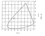
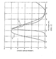
- the CIE chromaticity coordinates (calculated value) for luminescence from a blue light emitting organic layer is shown in Figure 4 and an enlarged view of Figure 4 is shown in Figure 5 .
- the value of the CIEx chromaticity coordinates is taken along the horizontal axis
- the value of the CIEy chromaticity coordinates is taken along the vertical axis.
- the CIEx chromaticity coordinate value is about 0.11-0.17 and the CIEy chromaticity coordinate value is about 0.07-0.29.
- the values of the CIEx chromaticity coordinates and the CIEy chromaticity coordinates periodically change with the change in the total optical path length of a transparent electrode and a blue light emitting organic layer.
- the CIEx chromaticity coordinate value exhibits a minimum value in the cycle (hereinafter referred to as minimum vale (Min)) and a maximum value in the cycle (hereinafter referred to as a maximum vale (Max)) at each of the following total optical path lengths.
- Min Minimum values (Min): about 200 nm, 470 nm, 750 nm, 970 nm
- the CIEy chromaticity coordinate value exhibits a minimum value in the cycle (hereinafter referred to as a minimum vale (Min)) and a maximum value in the cycle (hereinafter referred to as maximum vale (Max)) at each of the following total optical path lengths.
- Min Minimum values (Min): about 190 nm, 430 nm, 670 nm, 930 nm
- the change in the CIEy chromaticity coordinate value which gives a greater effect on the color tone, can be minimized by relating the total optical path length with a minimum value (Min) or maximum value (Max) of the CIEy chromaticity coordinates.
- the CIEy chromaticity coordinates value changes in the range of 0.2280 to 0.2384.
- the difference (b1) between the maximum and the minimum values is 0.0104.
- the CIEy chromaticity coordinates value changes in the range of 0.2219 to 0.2228, with the difference (b2) between the maximum and minimum values being as small as 0.0009, even if there is the fluctuation of ⁇ 20 nm in the total optical path length.
- the value is only 9% (0.104 x 9/100%, hereinafter calculated in the same manner) or less of the value when the total optical path length is related to neither a minimum value (Min) nor a maximum value (Max).
- the CIEy chromaticity coordinates value changes in the range of 0.2834 to 0.2848, with the difference (b3) between the maximum and minimum values being 0.0014.
- the value is only 14% or less of the value when the total optical path length is related to neither a minimum value (Min) nor a maximum value (Max).
- the method of causing the total optical path length of the transparent electrode and blue light emitting organic layer to be related to a minimum value (Min) or a maximum value (Max) of the CIE chromaticity coordinates value can be achieved by appropriately changing the refractive index of the transparent electrode, the thickness of the transparent electrode, the refractive index of the blue light emitting organic layer, and the thickness of the blue light emitting organic layer.
- An alternative preferable method is to provide an optical path length correction layer as shown in the fourth and fifth embodiments.
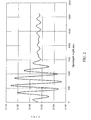
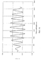
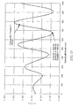
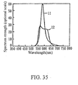
- Figure 6 is a drawing showing the relationship between an interference peak and the intensity peak when a blue light is emitted in the first embodiment.
- the interference peak is indicated by A1 and the intensity peak is indicated by B1.
- the total optical path length of a transparent electrode and a blue light emitting organic layer is 430 nm which is related to a minimum value (Min) of the CIEy chromaticity coordinates.
- interference factors are standardized so that the maximum value is 100 and the minimum value is 0 to clearly indicate the interference peak position.
- actual luminescence values are indicated without standardization.
- Figure 7 shows the relationship among the interference peak, intensity peak, and wavelength when a blue light is emitted by a conventional organic EL device.
- the interference peak is indicated by A2 and the intensity peak is indicated by B2.
- the total optical path length (nm) of the transparent electrode and the blue light emitting organic layer is 468 nm as indicated by B1 in Figure 5 in order to accord the interference peak A2 with the intensity peak B2.
- the CIEy chromaticity coordinate value exhibits neither a minimum value (Min) nor a maximum value (Max).
- the change in the CIE chromaticity coordinates value in the organic EL device of the first embodiment is decreased by relating the total optical path length of the transparent electrode and the organic layer to either a minimum value (Min) or a maximum value (Max), preferably to a minimum value (Min) of the CIEy chromaticity coordinates, even if there is the certain fluctuation in the total optical path length and there is a difference between the interference peak (A1) and the intensity peak (B1). This eventually decreases a visual blue color change.
- the change in the CIE chromaticity coordinates value due to the fluctuation of the total optical path length is bigger and significant problems even if the interference peak A2 is coincided with the intensity peak B2. As a result, the change in a visualized blue color becomes bigger and significant problems.
- the value of EL luminescence somehow decreases by the discrepancy of the interference peak (A1) of a blue light emitting organic layer and the intensity peak (B1) in the organic EL device of the first embodiment, the decrease is as small as about 7% as compared with a conventional organic EL device in which the interference peak (A2) and the intensity peak (B2) are identical.
- the decrease of EL luminescence there are no problems in practical use.
- a further decrease in the change of the CIE chromaticity coordinate value due to the fluctuation of the total optical path length of the transparent electrode and the blue light emitting organic layer has been confirmed to be achieved by increasing the thickness of the blue light emitting organic layer to 2,000 nm or more, preferably 3,000 nm or more, and more preferably 5,000 nm or more, as indicated by Figures 32 and 33 .
- the organic EL device is for an application in which it is possible to increase the thickness of the blue light emitting organic layer, a more excellent color tone and a blue color with minimal color change can be realized not only by making the total optical path length that exhibiting either a maximum value (Max) or a minimum value (Min) in the CIE chromaticity coordinates, but also by increasing the thickness of the blue light emitting organic layer.
- the organic layer is formed with including the organic light-emitting layer at least, and more preferably, it's voluntary consist of the hole injection layer, the hole transportation layer, the hole barrier layer, the electron injection layer, the electron transportation layer and electron barrier layer.
- the typical construction of the layers will be explained by following.
- the organic layer includes the blue organic light-emitting material in the first embodiment.
- the blue organic light-emitting material is not specifically restricted, it preferably has the following three functions at the same time for example.
- the organic light-emitting layer contains one or more aromatic compounds having a styryl group.
- aromatic compounds having this styryl group excellent emitting property and the durability may be obtained.
- the organic light-emitting layer may further comprise other compounds.
- Such other compounds include fluorescent whitening agents such as benzothiazoles, benzoimidazoles, benzooxazoles, and the like; metal chelated oxinoid compounds and styrylbenzene compounds.
- fluorescent whitening agents such as benzothiazoles, benzoimidazoles, benzooxazoles, and the like
- metal chelated oxinoid compounds such as benzothiazoles, benzoimidazoles, benzooxazoles, and the like
- metal chelated oxinoid compounds such as benzothiazoles, benzoimidazoles, benzooxazoles, and the like
- metal chelated oxinoid compounds such as benzothiazoles, benzoimidazoles, benzooxazoles, and the like
- metal chelated oxinoid compounds such as benzothiazoles, benzoimidazoles, benzooxazoles, and the like
- fluorescent bleaching agents including a benzoxazole compound such as 2,5-bis(5,7-di-t-pentyl-2-benzoxazolyl)-1,3,4-thiadiazole, 4,4'-bis(5,7-di-t-pentyl-2-benzoxazolyl)stilbene, 4,4'-bis(5,7-di-(2-methyl-2-butyl)-2-benzoxazolyl)stilbene, 2,5-bis(5,7-di-t-pentyl-2-benzoxazolyl)thiophene, 2,5-bis(5- ⁇ , ⁇ -dimethylbenzyl-2-benzoxazolyl)thiophene, 2,5-bis(5-7-di(2-methyl-2-butyl)-2-benzoxazolyl)-3,4diophenylthiophene,
- a benzoxazole compound such as 2,5-bis(5,7-di-t-pentyl-2-benzoxazoly
- the compounds disclosed in JP-A-63-295695 can be used.
- typical examples are 8-hydroxyquinoline metal complexes such as tris(8-quinolinol) aluminum, bis(8-quinolinol) magnesium, bis(benzo[f]-8-quinolinol) zinc, bis(2-methyl-8-quinolinolate) aluminum oxide, Tris(8-quinolinol) indium, tris(5-methyl-8-quinolinol) aluminum, 8-quinolinollithium, tris(5-chloro-8-quinolinol) gallium, bis(5-chloro-8-quinolinol) calcium, poly[zinc(II)-bis(8-hydroxy-5-quinolinonyl)methane],and the like and dilithium epinetridione.
- styryl benzene compounds and derivatives the compounds disclosed in the specifications of EPCs No. 0319881 and No. 0373582 can be also used.
- Typical examples of these styryl benzene compounds are 1,4-bis(2-methylstyryl)benzene, 1,4-bis(3-methylstyryl)benzene, 1,4-bis(4-methylstyryl)benzene, distyrylbenzene, 1,4-bis(3-ethylstyryl)benzene, 1,4-bis(2-methylstyryl)-2-methylbenzene, 1,4-bis(2-methylstyryl)-2-ethylbenzene, and the like.
- distyryl pyrazine derivatives disclosed in JP-A-2-252793 can be used as the material for the emitting layer.
- Typical examples of these derivatives are 2,5-bis(4-methylstyryl)pyrazine,2,5-bis(4-ethylstyryl)pyrazine, 2,5-bis[2-(1-naphthyl)vinyl]pyrazine, 2,5-bis(4-methoxystyryl)pyrazine, 2,5-bis[2-(4-biphenyl)vinyl] pyrazine, 2,5-bis[2-(1-pyrenyl)vinyl]pyrazine, and the like.
- the polyphenyl compounds disclosed in the specification of EPC No. 0387715 can be used as the material for the emitting layer.
- the following compounds can be used as the material for the emitting layer: 12-phthaloperinone ( J. Appl. Phys., Vol 27, L713, (1988 )), 1,4-diphenyl-1,3-butadiene, 1,1,4,4-tetraphenyl-1,3 butadiene( Appl. Phys.
- aromatic dimethylidine compounds compounds disclosed in the specification of EPC No. 0388768 or JP-A-3-231970 .
- aromatic dimethylidine compounds compounds disclosed in the specification of EPC No. 0388768 or JP-A-3-231970 .
- Specific Examples of such compounds are 1,4-phenylenedimethylidyne, 4,4-phenylenedimethylidyne, 2,5-xylenedimethylidyne, 2,6-naphthylenedimethylidyne, 1,4-biphenylenedimethylidyne, 1,4-pterephenylenedimethylidyne, 9,10-anthracenediyldimethylidyne, 4,4'-bis(2,2-di-t-butylphenylvinyl), 4,4'-bis(2,2-diphenylvinyl), and derivatives of these.
- organic light-emitting materials comprising a dopant such as coumarin compounds and the like which can enhance the blue color light to red color light into the host materials such as an organic light-emitting material having distyrylaryllen moiety, for example, 4,4-bis(2,2-diphenylbinyl) biphenyl and the like.
- the thickness of the organic light-emitting layer may be determined in considering the optical path length, and usually it is favorable in the range of 5nm to 5 micrometer. This reason is that if the thickness of the organic light-emitting layer is below 5 nm, the light emitting strength and the durability may decrease.
- the injection voltage may increase.
- the thickness of the organic light-emitting layer is favorably in the range of 10 nm to 3 micrometer and more favorably in the range of 20 nm to 1 micrometer.
- the organic light-emitting layer may be structured of one layer made from one or more of the above materials, or may be a plural of layers in which one organic light-emitting layer made from compounds differing from the compound of the other layer are laminated on other layer.
- any material optionally selected from photoconductive materials conventionally used as a material for transferring a charge of holes and from known materials used for a hole injecting layer of an organic EL device can be used as the material for the hole injecting layer provided as required.
- the material for the hole injecting layer which has a function either as a hole injecting layer or as a barrier for an electron may be either an organic or inorganic compound.
- the above compounds can be used.
- polphyrin compounds disclosed in JP-A-63-2956965
- aromatic tertiary amines and styrylamine compounds see the specifications USP No.
- porphyrin compounds are porphin, 1,10,15,20-tetraphenyl-21H, 23H-porphin copper (II), 1,10,15,20-tetraphenyl-21H, 23H-porphin zinc (II), 5,10,15,20-tetrakis(pentafluorophenyl)-21H, 23H-porphin, silicon phthalocyanine oxide, aluminum phthalocyanine chloride, phthalocyanine (non-metal), dilithium phthalocyanine, copper tetramethylphthalocyanine, copper phthalocyanine, chromium phthalocyanine, zinc phthalocyanine, lead phthalocyanine, titanium phthalocyanine oxide, magnesium phthalocyanine, copper octamethylphthalocyanine, and the like.
- Typical examples of the above aromatic tertiary amine and styrylamine compounds are N,N,N',N'-tetraphenyl-4,4'-diaminophenyl, N,N'-diphenyl-N,N'-bis-(3-methylphenyl)-[1,1'-biphenyl]-4,4'-diamine (hereinafter abbreviated as "TPD"), 2,2-bis (4-di-p-tolylaminophenyl)propane, 1,1-bis(4-di-p-tolylaminophenyl)cyclohexane, N,N,N',N'-tetra-p-tolyl-4,4'-diaminophenyl, 1,1-bis(4di-p-tolylaminophenyl)-4-phenylcyclohexane, bis(4-dimethylamino-2-methylphenyl)phenylmethane, bis(
- aromatic dimethylidine compounds shown as the material for the emitting layer can be utilized as the material used for the hole injecting layer.
- the thickness of the hole injecting layer there are no restrictions to it, but it is favorable to be generally in the range of 5 nm to 5 micrometer.
- this hole injecting layer may be structured of one layer made from one or more of the above materials or may be a layer in which other hole injecting layers made from compounds differing from the compound of that layer are laminated on that layer.
- the electron injecting layer provided as required may have the function of transferring, to the emitting layer, the electrons injected from the cathode.
- Optional compounds selected from conventionally known compounds may be used.
- Typical examples of these compounds include nitro-substituted fluorene derivatives; anthraquinodimethane derivatives disclosed in JP-A-57-149259 , JP-A-58-55450 , and JP-A-63-104061 ; diphenylquinone derivatives, thiopyrane dioxide derivatives, heterocyclic tetracarboxylic acid anhydrides such as naphthaleneperillene and the like, and carbodiimides which are all disclosed in Polymer Preprints, Japan Vol. 37. No. 3 (1988) p.
- metal complexes of 8-quinolinole specifically, tris(8-quinolinole) aluminum (hereinafter abbreviated as "Alq"), tris(5,7-dibromo-8-quinolinole) aluminum, tris(2-methyl-8-quinolinole) aluminum, and metal complexes produced by replacing the Primary metals of these metal complexes with In, Mg, Cu, Ca, Sn, Ga, or Pb.
- Alq tris(8-quinolinole) aluminum
- Alq tris(5,7-dibromo-8-quinolinole) aluminum
- 2-methyl-8-quinolinole tris(2-methyl-8-quinolinole) aluminum
- metal complexes produced by replacing the Primary metals of these metal complexes with In, Mg, Cu, Ca, Sn, Ga, or Pb metal-free or metal phthalocyanine compounds of 8-quinolinole derivatives or compounds produced by replacing the terminal group of these compounds with an alkyl group
- This electron injecting layer may be structured of one layer made from one or more of the above materials or may be a layer in which other electron injecting layers made from compounds differing from the compound of that layer are laminated on that layer.
- the thickness of the electron injecting layer is generally from 5 nm to 5 micrometer.
- the thickness of the electron injecting layer is below 5 nm, the light emitting strength and the durability may decrease. To the contrary, if the thickness of the electron injecting layer is over 5 micrometer, the injection voltage may increase.
- the thickness of the electron injecting layer is favorably in the range of 10 nm to 3 micrometer and more favorably in the range of 20 nm to 1 micrometer.
- metals, alloys, electrically conductive compounds with a large work function for example, 4 eV or more
- a large work function for example, 4 eV or more
- ITO indium tin oxide
- CuI copper iodide
- tin oxide zinc oxide
- gold platinum, palladium, and the like
- the thickness of the anode layer is not specifically restricted, such a thickness is preferably in the range of 10 to 1,000 nm, and more preferably 10 to 200 nm.
- metals, alloys, electric conductive compounds with a small work function (for example, less than 4 eV), or mixtures thereof may be used to obtain the good electron injection property.
- a small work function for example, less than 4 eV
- magnesium, aluminum, indium, lithium, sodium, silver, and the like may be used either individually or in combination of two or more.
- the thickness of the cathode layer is not specifically restricted, such a thickness is preferably in the range of 10 to 1,000 nm, and more preferably 10 to 200 nm.
- each anode or cathode should be transparent.
- Support substrates will be explained. Any materials for such support substrates which can show the good mechanical property, low moisture permeability and oxygen permeability and which are usually used for the conventional EL device may be used. Such materials include glasses, ceramics and the like.
- the organic EL device of the first embodiment of the following structure (i) has been described, it is also preferable to employ the following structures (ii) to (iv) in which other structural elements such as a hole injection layer and an electron injection layer are combined.
- the substrate may be provided below the cathode layer as well as the anode layer.
- the EL device of the first embodiment should be a full color type display.
- GCCM green color conversion layer
- Figure 28 the relationship between the total optical path including the GCCM and the CIEy chromaticity coordinates is shown in Figure 28
- Figure 29 the relationship between the total optical path including the GCCM and the CIEy chromaticity coordinates is shown in Figure 29 .
- RCCM red color conversion layer
- CIEx chromaticity coordinates the relationship between the total optical path including the RCCM and the CIEx chromaticity coordinates is shown in Figure 30
- CIEy chromaticity coordinates the relationship between the total optical path including the RCCM and the CIEy chromaticity coordinates is shown in Figure 31 .
- the organic EL device of the second embodiment is substantially the same as that of the first embodiment shown in Figure 2 , wherein the former employs a green light emitting organic layer with a intensity peak wavelength (S3) of 500 to 570 nm as organic light-emitting layer.
- the total optical path length (t3) of the transparent electrode and the green light emitting organic layer satisfies the inequality, Max - 20 nm ⁇ t3 ⁇ Max + 20 nm, wherein Max is the maximum optical path length at which the CIEy chromaticity coordinates measured according to JIS Z 8701 exhibits a maximum value.
- Figure 8 is a drawing showing the relationship between the total optical path length (t3) of a transparent electrode and a green light emitting organic layer and the CIEx chromaticity coordinate value of EL luminescence.
- the value (nm) of the total optical path length (t3) is taken along the horizontal axis
- the value of the CIEx chromaticity coordinates is taken along the vertical axis.
- Figure 9 is a drawing showing the relationship between the total optical path length (t3) of a transparent electrode and a green light emitting organic layer and the CIEy chromaticity coordinate value of EL luminescence.
- the value (nm) of the total optical path length (t3) is taken along the horizontal axis
- the value of the CIEy chromaticity coordinates is taken along the vertical axis.
- the CIE chromaticity coordinates (calculated value) for luminescence from a green light emitting organic layer is shown in Figure 10 and an enlarged view of Figure 10 is shown in Figure 11 .
- the value of the CIEx chromaticity coordinates is taken along the horizontal axis
- the value of the CIEy chromaticity coordinates is taken along the vertical axis.
- the CIEx chromaticity coordinate value is about 0.15-0.33 and the CIEy chromaticity coordinate value is about 0.60-0.75.
- the values of the CIEx chromaticity coordinates and the CIEy chromaticity coordinates periodically change with the change in the total optical path length of a transparent electrode and a green light emitting organic layer.
- the CIEx chromaticity coordinate value exhibits a minimum value in the cycle (hereinafter referred to as minimum vale (Min)) and a maximum value in the cycle (hereinafter referred to as maximum vale (Max)) at each of the following total optical path lengths.
- Min Minimum values (Min): about 200 nm, 470 nm, 745 nm
- the CIEy chromaticity coordinate value exhibits a minimum value in the cycle (hereinafter referred to as minimum vale (Min)) and a maximum value in the cycle (hereinafter referred to as maximum vale (Max)) at each of the following total optical path lengths.
- Min Minimum values (Min): about 100 nm, 360 nm, 640 nm, 910 nm
- the change in the CIEy chromaticity coordinate value which gives a greater effect on the color tone, can be minimized by relating the total optical path length with a minimum value (Min) or a maximum value (Max) of the CIEy chromaticity coordinates.
- the CIEy chromaticity coordinates value changes in the range of 0.6482 to 0.6502.
- the difference between the maximum and minimum values is 0.0020.
- the CIEy chromaticity coordinates value changes in the range of 0.6502 to 0.6505, with the difference between the maximum and minimum values being as small as 0.0003, even if there is the fluctuation of ⁇ 20 nm in the total optical path length.
- the value is only 10% or less of the value when the total optical path length is not related to a maximum value (Max).
- the CIEy chromaticity coordinates value changes in the range of 0.6239 to 0.6243 even if there is the fluctuation of ⁇ 20 nm in the total optical path length.
- the difference between the maximum and minimum values is 0.0004. Specifically, the value is only 20% or less of the value when the total optical path length is not related to a minimum value (Min).
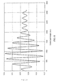
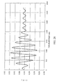
- Figure 12 is a drawing showing the relationship between an interference peak and the intensity peak when a green light is emitted in the second embodiment.
- the interference peak is indicated by A1 and the intensity peak is indicated by B1.
- the total optical path length of a transparent electrode and a green light emitting organic layer is 497 nm which is related to a maximum value (Max) of the CIEy chromaticity coordinates.
- the interference factors are standardized so that the maximum value is 100 and the minimum value is 0 to clearly indicate the interference peak position.
- actual luminescence values are indicated without standardization.
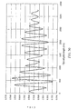
- Figure 13 shows the relationship among the interference peak, intensity peak, and wavelength when a green light is emitted by a conventional organic EL device.
- the interference peak is indicated by A2 and the intensity peak is indicated by B2.
- the total optical path length (nm) of the transparent electrode and the green light emitting organic layer is 517 nm as indicated G1 in Figure 11 in order to accord the interference peak A2 with the intensity peak B2.
- the CIEy chromaticity coordinate value exhibits neither a maximum value (Max) nor a minimum value (Min).
- the change in the CIE chromaticity coordinates value in the organic EL device of the second embodiment is decreased by relating the total optical path length of the transparent electrode and the green organic layer to either a maximum value (Max) or a minimum value (Min), preferably to a maximum value (Max) of the CIEy chromaticity coordinates, even if there is the certain fluctuation in the total optical path length and there is a difference between the interference peak (A1) and the intensity peak (B1). This eventually decreases a color change.
- the change in the CIEy chromaticity coordinates value originating from the fluctuation of the total optical path length is bigger and significant problems even if the interference peak A2 is coincided with the intensity peak B2. As a result, the change in a visualized green color becomes bigger and significant problems.
- the value of EL luminescence is somehow decreased by the discrepancy of the interference peak (A1) of a green light emitting organic layer and the intensity peak (B1) in the organic EL device of the second embodiment, the decrease is as small as about 2% as compared with a conventional organic EL device in which the interference peak (A2) and the intensity peak (B2) are identical.
- the decrease of the EL luminescence there are no problems in practical use.
- the organic EL device 116 of the third embodiment has a blue light emitting organic layer 30 of which the intensity peak wavelength is between 400 and 490 nm, a green light emitting organic layer 32 of which the intensity peak wavelength is between 500 and 570 nm, and a red light emitting organic layer 34 of which the intensity peak wavelength is between 580 and 700 nm, each formed between a transparent electrode layer (an anode layer) 10 and a cathode layer 12, with the resulting layers being formed on a glass substrate 22.
- the total optical path length (t1) of the transparent electrode 10 and the blue light emitting organic layer 30 satisfies the inequality Min - 20 nm ⁇ t1 ⁇ Min + 20 nm, wherein Min is the optical path length at which the CIEy chromaticity coordinates measured according to JIS Z 8701 exhibits a minimum value.
- the total optical path length (t3) of the transparent electrode 10 and the green light emitting organic layer 32 satisfies the inequality, Max - 20 nm ⁇ t3 ⁇ Max + 20 nm, wherein Max is the optical path length at which the CIEy chromaticity coordinates measured according to JIS Z 8701 exhibits a maximum value.
- the total optical path length (t2) of the transparent electrode 10 and the red light emitting organic layer 34 satisfies the inequality, Max - 20 nm ⁇ t3 ⁇ Max + 20 nm, wherein Max is the optical path length at which the CIEx chromaticity coordinates measured according to JIS Z 8701 exhibits a maximum value.
- the organic EL device of the third embodiment is the same as that of the first embodiment, except that the former has not only a blue light emitting organic layer 30 of which the intensity peak wavelength is between 400 and 490 nm, but also a green light emitting organic layer 32 of which the intensity peak wavelength is between 500 and 570 nm, and a red light emitting organic layer 34 of which the intensity peak wavelength is between 580 and 700 nm, as organic layers.
- the green light emitting organic layer of which the intensity peak wavelength is between 500 and 570 nm is same as that of the second embodiment.
- the following description will be focused on the red light emitting organic layer 34 of which the intensity peak wavelength is between 580 and 700 nm, and the description on other components may be omitted as the case allows.
- Figure 15 is a drawing showing the relationship between the total optical path length (t2) of a transparent electrode and a red light emitting organic layer and the CIEx chromaticity coordinate value of EL luminescence.
- the value (nm) of the total optical path length (t2) is taken along the horizontal axis
- the value of the CIEx chromaticity coordinates is taken along the vertical axis.
- Figure 16 is a drawing showing the relationship between the total optical path length (t2) of a transparent electrode and a red light emitting organic layer and the CIEy chromaticity coordinate value of EL luminescence.
- the value (nm) of the total optical path length (t2) is taken along the horizontal axis
- the value of the CIEy chromaticity coordinates is taken along the vertical axis.
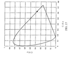
- the CIE chromaticity coordinates (calculated value) for luminescence from a red light emitting organic layer is shown in Figure 17 and an enlarged view of Figure 17 is shown in Figure 18 .
- the value of the CIEx chromaticity coordinates is taken along the horizontal axis
- the value of the CIEy chromaticity coordinates is taken along the vertical axis.
- the CIEx chromaticity coordinate value is about 0.60-0.70 and the CIEy chromaticity coordinate value is about 0.30-0.38.
- the values of the CIEx chromaticity coordinates and the CIEy chromaticity coordinates periodically change with the change in the total optical path length of a transparent electrode and a red light emitting organic layer.
- the CIEx chromaticity coordinate value exhibits a minimum value in the cycle (hereinafter referred to as minimum vale (Min)) and a maximum value in the cycle (hereinafter referred to as maximum vale (Max)) at each of the following total optical path lengths.
- Min Minimum values (Min): about 230 nm, 530 nm, 820 nm
- the CIEy chromaticity coordinate value exhibits a minimum value in the cycle (hereinafter referred to as minimum vale (Min)) and a maximum value in the cycle (hereinafter referred to as maximum vale (Max)) at each of the following total optical path lengths.
- Min Minimum values (Min): about 100 nm, 390 nm, 690 nm, 980 nm
- the change in the CIEx chromaticity coordinate value which gives a greater effect on the color tone, can be minimized by relating the total optical path length with a minimum value (Min) or maximum value (Max) of the CIEx chromaticity coordinates.
- the total optical path length of the transparent electrode and the red light emitting organic layer is 596 nm as indicated by R1 in Figure 18 , wherein the total optical path length is related to neither a minimum value (Min) nor maximum value (Max) of the CIEx chromaticity coordinates value, and has the fluctuation of ⁇ 20 nm, the CIEx chromaticity coordinates value changes in the range of 0.6231 to 0.6247.
- the difference between the maximum and minimum values is 0.0016.
- the total optical path length (t2) of the transparent electrode and the red light emitting organic layer (t2) is 523 nm as indicated by R2 in Figure 18 , wherein the total optical path length is related to a minimum value (Min) of the CIEx chromaticity coordinates value
- the CIEx chromaticity coordinate value changes in the range of 0.6202 to 0.6203, with the difference between the maximum and minimum values being as small as 0.0001, even if there is the fluctuation of ⁇ 20 nm in the total optical path length.
- the value is only 7% or less of the value when the total optical path length is not related to a minimum value (Min).
- the total optical path length (t2) of the transparent electrode and the red light emitting organic layer is 688 nm as indicated by R3 in Figure 18 , wherein the total optical path length is related to maximum value (Max) of the CIEx chromaticity coordinates value
- the CIEx chromaticity coordinates value changes in the range of 0.6295 to 0.6296.
- the difference between the maximum and minimum values is 0.0001.
- the value is only 7% or less of the value when the total optical path length is not related to a maximum value (Max).
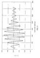
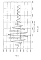
- Figure 19 is a drawing showing the relationship between an interference peak and the intensity peak when a red light is emitted in the third embodiment.
- the interference peak is indicated by A1 and the intensity peak is indicated by B1.
- the total optical path length of a transparent electrode and a red light emitting organic layer is 680 nm which is related to a maximum value (Max) of the CIEx chromaticity coordinates.
- the interference factors are standardized so that the maximum value is 100 and the minimum value is 0 to clearly indicate the interference peak position.
- actual intensity values are indicated without standardization.
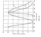
- Figure 20 shows the relationship among the interference peak, intensity peak, and wavelength when a red light is emitted by a conventional organic EL device.
- the interference peak is indicated by A2 and the intensity peak is indicated by B2.
- the total optical path length (nm) of the transparent electrode and the red light emitting organic layer is 596 nm as indicated by R1 in Figure 18 in order to accord the interference peak A2 with the intensity peak B2.
- the color change in the red light emitting organic layer of the third embodiment is decreased by relating the total optical path length of the transparent electrode and the red organic layer to either a maximum value (Max) or a minimum value (Min), preferably to a maximum value (Max) or minimum value (Min) of the CIEx chromaticity coordinates, even if there is the certain fluctuation in the total optical path length and there is a difference between the interference peak (A1) and the intensity peak (B1).
- the change in the CIEx chromaticity coordinates value originating from the fluctuation of the total optical path length is bigger and significant problems even if the interference peak A2 is coincided with the intensity peak B2. As a result, the change in a visualized red color becomes bigger and significant problems.
- the value of EL luminescence is somehow decreased by the discrepancy of the interference peak (A1) of a red light emitting organic layer and the intensity peak (B1) in the organic EL device of the third embodiment, the decrease is as small as about 20% as compared with a conventional organic EL device in which the interference peak (A2) and the intensity peak (B2) are identical.
- the decrease of the EL luminescence there are no problems in practical use.
- an organic EL device 120 of the fourth embodiment has an optical path length correction layer 20, a transparent electrode layer (an anode layer) 10, a blue light emitting organic layer 12 of which the intensity peak wavelength (S1) is between about 400 and 490 nm, and a cathode layer 16 formed on a glass substrate 22 in that order.
- the total optical path length (t4) of the transparent electrode 10 and the blue light emitting organic layer 12 satisfies the inequality Min - 20 nm ⁇ t4 ⁇ Min 20 nm, wherein Min is the minimum optical path length at which the CIEy chromaticity coordinates measured according to JIS Z 8701 exhibits a minimum value.
- the organic EL device of the fourth embodiment is same as that of the first embodiment, except that an optical path length correction layer 20 is provided between a transparent electrode layer (an anode layer) 10 and a blue light emitting organic layer 12, and the total optical path length (t4) is limited in the fixed range.
- the transparent electrode is not necessarily the anode layer, but the cathode layer may be the transparent layer, or both the anode layer and cathode layer may be the transparent layer. However, when both the anode layer and the cathode layer are transparent layers, the length of the anode layer and the cathode layer is further added to the total optical path length.
- Figure 7 is a drawing showing the relationship among the interference factor by the blue light emitting organic layer, radiant intensity spectrum, and wavelength (nm) in a conventional organic EL device.
- the total optical path length (t3) of the transparent electrode and blue light emitting organic layer is 468 nm, which is related to neither a maximum value (Max) nor minimum value (Min) of the CIEx chromaticity coordinates or the CIEy chromaticity coordinates, as can be seen from Figures 2 and 3 .
- the total optical path length (t1) of the transparent electrode and blue light emitting organic layer which coincides with, for example, a minimum vale (Min) of the CIEx chromaticity coordinates or the CIEy chromaticity coordinates, is selected from Figures 2 and 3 .
- any minimum value (Min) among three to four minimum values (Min) indicated in Figures 2 and 3 may be used in selecting the total optical path length (t1). It is preferable, however, to select the minimum value (Min) around which the values for the CIEx chromaticity coordinates and the CIEy chromaticity coordinates exhibit least fluctuation. The fluctuation in the CIEx chromaticity coordinate value and the CIEy chromaticity coordinate value due to the change in the total optical path length may be minimized by selecting such a minimum value (Min).
- the difference between the total optical path length of the transparent electrode and blue light emitting organic layer in a conventional organic EL device and the total optical path length (t1) of the transparent electrode and blue light emitting organic layer corresponding to the selected the minimum value (Min) for the CIEx chromaticity coordinates and the CIEy chromaticity coordinates is the optical path length due to the optical path length correction layer.
- the thickness for the optical path length correction layer and other constitution materials may be selected so that such an optical path length for correction may be added.
- the optical path length 670 nm which corresponds to one of the minimum values (Min) of the CIEy chromaticity coordinates
- 468 nm which is the total optical path length of the transparent electrode and blue light emitting organic layer before the optical path length correction
- the resultant optical path length 202 nm should be the length for the optical path length correction layer.
- Providing the optical path length correction layer makes it unnecessary to increase the thickness of the organic material layer to be provided between the electrodes for optical correction, thereby obviating a voltage rise due to a thick organic material layer. This is additional advantage of the optical path length correction layer.
- Inorganic and organic substances may be used without specific limitations as the material for the optical path length correction layer.
- inorganic substances glass, quartz, oxides such as tin oxide, indium oxide, lead oxide, aluminum oxide, and lithium oxide, fluorides such as lithium fluoride, calcium fluoride, and magnesium fluoride, and the like may be used.
- metals such as gold, silver, copper, aluminum, and molybdenum, which are transparent in a thin film, may be used.
- These inorganic substances may be used either individually or in combination of two or more.
- organic EL materials organic EL materials, polypropylene resins, polyethylene resins, fluorine-containing resins, acrylic resins, polyether sulfone resins, polycarbonate resins, and the like are given. These organic substances may be used either individually or in combination of two or more. These substances must allow electric charges to pass through when formed between electrodes, but may be a complete insulating material when formed outside the electrodes.
- the refractive index of the material is preferably in the range of 1.0 to 3.0 (determined by Abbe's refractometer at 25°C. It is difficult to find available materials with a refractive index of less than 1.0. On the other hand, the selection of materials is unduly limited if the required refractive index is more than 3.0.
- the refractive index of the material is preferably between 1.3 and 2.5, and more preferably between 1.7 and 2.1.
- the thickness of the optical path length correction layer is not specifically restricted, this thickness is preferably in the range of 1 nm to 2,000 nm, for example. If the thickness of the optical path length correction layer is less than 1 nm, it may be difficult to form a uniform thickness layer or the effect of the optical path length correction layer may not be sufficient. On the other hand, if the optical path length correction layer is thicker than 2,000 nm, the effect of an uneven thickness of the optical path length correction layer may not be neglected, so that it may be difficult to adjust the total optical path length of the transparent electrode layer and the organic light emitting layer.
- the thickness of the optical path length correction layer is more preferably between 2 nm and 500 nm, and still more preferably between 5 nm and 100 nm.
- the method of forming the optical path length correction layer is not specifically limited, a vapor deposition method, sputtering method, EB (Electron Beam) method, MBE (Molecular Beam Epitaxy) method, LB (Langumuir Blodgett) method, CVD (Chemical Vapor Deposition) method, spin coat method, and casting method, for example, are preferable.
- the organic EL device 120 of the fourth embodiment with the following structure (i) comprising the optical path length correction layer 20 between the substrate and the transparent electrode layer (anode layer) 10, as shown in Figure 21 , has been described, it is also preferable to employ the following structures (ii) to (vii) in which other structural elements such as a hole injection layer and an electron injection layer are combined.
- the structures (i) and (v) to (vii), in which the optical path length correction layer is provided between the substrate and the anode layer, are particularly preferable because these do not alter the structure of the anode layer/organic light-emitting layer/cathode layer in conventional organic EL devices.
- the substrate is not necessarily limited to an anode base, but a cathode base is also acceptable.
- the number optical path length correction layer is not necessarily limited to one, but two optical path length correction layers as in the following structure (iv) is also acceptable.
- the fifth embodiment is a method of manufacturing the organic EL device 120 of the fourth embodiment.
- the method comprises a step of forming the transparent electrode, organic layer, and optical path length correction layer so that the total optical path length (t) (nm) of the transparent electrode, organic layer, and optical path length correction layer satisfies the following inequality (a) or inequality (b) or both: wherein Min is the optical path length (nm) at which the CIEx chromaticity coordinates or CIEy chromaticity coordinates measured according to JIS Z 8701 exhibit a minimum value, and Max is the optical path length (nm) at which the CIEx chromaticity coordinates or CIEy chromaticity coordinates measured according to JIS Z 8701 exhibit a maximum value.
- Min 20 ⁇ nm ⁇ t ⁇ Min + 20 ⁇ nm Max - 20 ⁇ nm ⁇ t ⁇ Max + 20 ⁇ nm
- the fifth embodiment comprise a step of preparing a substrate, a step of forming an optical path length correction layer, a step of forming an anode layer (a transparent electrode), a step of forming an organic layer, and a step of forming a cathode layer in that order.
- the step of forming an anode layer may be just providing a substrate made from a transparent electrode of a prescribed material having a prescribed thickness, and using this substrate as is.
- the step of forming the optical path length correction layer which is a feature of the fifth embodiment, may be performed after the determination of the thickness and material for construction of the optical path length correction layer as described in the fourth embodiment. Thereafter, the optical path length correction layer is formed on the substrate.
- the vacuum deposition method for example, as also described in the fourth embodiment can be used as the method of forming. Then, a conventional organic EL device described in the fourth embodiment may be formed on the optical path length correction layer.
- the conditions for the conventional fabrication method of organic EL devices may be basically employed as is.
- a method of fabrication comprising forming a first optical path length correction layer on the substrate, forming an anode layer thereon, and then forming a second optical path length correction layer may also be used. This method ensures fabrication of an organic EL device with three primary colors (red, blue, green), each requiring the individual material of construction and thickness for the optical path length correction layer.
- a transparent electrode film with a thickness of 130 nm was formed from ITO as an anode layer 10 on a transparent glass substrate 22 with a dimension of 1.1 mm (thickness) x 200 mm (length) x 200 mm (width).
- the glass substrate 22 and the anode layer 10 are collectively called a substrate 30 in the following description.
- This substrate 30 was cleaned in isopropyl alcohol with the ultrasonic cleaner, dried in a nitrogen gas atmosphere, and washed for 10 minutes using UV (ultraviolet radiation) and ozone.
- the vapor deposition material container 212A was filled with 4,4'-bis(2,2-diphenylvinyl)biphenyl (hereinafter referred to as (DPVBi)) which forms an organic light-emitting layer 12
- the container 212B was filled with 4,4'-bis[2-(4-(N,N-di-p-tolyl)phenyl)vinyl]biphenyl (hereinafter referred to as (DTAVBi)) which forms an organic light-emitting layer
- the container 212C was filled with tris(8-quinolinol)aluminum (hereinafter referred to as (Alq)) which forms an electron injection layer 14
- the container 212D was filled with a reducing doping material (Li) which forms part of the electron injection layer 14
- the container 212E was filled with a metal (A
- an organic blue light emitting layer 12 formed from DPVBi and DTAVBi, an electron injection layer 14 formed by simultaneous vapor deposition of Alq and Li, and a cathode layer 16 made of aluminum were laminated in that order on a transparent electrode (ITO film) 10 of the substrate 30, thereby obtaining an organic EL device.
- the total optical path length (t1) of the transparent electrode and the blue light emitting organic layer was set at 430 nm at which the CIEy chromaticity coordinates exhibit a minimum value (Min).
- Thickness of the transparent electrode (refractive index 1.7): 130 nm
- Thickness of the organic light emitting layer (refractive index 1.7): 80 nm
- Thickness of the electron injection layer (refractive index 1.7): 43 nm
- Thickness of the cathode layer 200 nm
- a DC voltage of 7V was applied between the cathode layer 16 (minus (-) electrode) and the transparent electrode 10 (plus (+) electrode) of the resulting organic EL device 100.
- the current density was 1.3 mA/cm 2 and the luminance measured by using a luminance meter was 39 cd/m 2 (the luminance was measured in the same manner in the following examples).
- Half life means the period of time required for luminance to become one half of the maximum luminance.
- the half life is a period of time required for the maximum luminance of 100 cd/m 2 to become one half of that value, 50 cd/m 2 .
- Example 2 an organic EL device was prepared in the same manner as in Example 1, except for using a green organic light emitting layer (thickness 120 nm) made by vapor deposition of Alq and coumarin 6 with the total optical path length (t3) of 497 nm, close to 500 nm at which the CIEy exhibits a maximum optical path length (Max).
- a green organic light emitting layer thinness 120 nm
- t3 total optical path length
- the performance of the organic EL device was evaluated by applying a DC voltage of 7V to confirm that the current density was 1.1 mA/cm 2 and luminance was 70 cd/m 2 .
- Example 3 an organic EL device was prepared in the same manner as in Example 1, except for using a red organic light emitting layer (thickness 57 nm) made by vapor deposition of Alq and 4-dicyanomethylene-2-methyl-6-(P-dimethylaminostyryl)-4H-pyrane with the total optical path length (t2) of 390 which coincides with an optical path length at which the CIEx exhibits a maximum value (Max).
- a red organic light emitting layer thinness 57 nm
- 4-dicyanomethylene-2-methyl-6-(P-dimethylaminostyryl)-4H-pyrane with the total optical path length (t2) of 390 which coincides with an optical path length at which the CIEx exhibits a maximum value (Max).
- the performance of the organic EL device was evaluated by applying a DC voltage of 7V between the electrodes to confirm that the current density was 0.98 mA/cm 2 and luminance was 25 cd/m 2 .
- Example 4 an organic EL device was prepared in the same manner as in Example 1, except that a magnesium oxide layer (thickness: 20 nm) was inserted between the glass substrate and the transparent electrode as an optical path length correction layer and an organic light emitting layer with a thickness of 58 nm was used.
- the total optical path length was 430 nm which coincides with the optical path length at which CIEy exhibits a minimum value (Min).
- the performance of the organic EL device was evaluated by applying a DC voltage of 7V between the electrodes to confirm that the current density was 1.1 mA/cm 2 and luminance was 33 cd/m 2 .
- Example 5 an organic EL device was prepared in the same manner as in Example 1, except that a magnesium oxide layer (thickness: 20 nm) was inserted between an electronic injection layer and a cathode, and an organic light emitting layer with a thickness of 58 nm was used.
- the total optical path length was 430 nm which coincides with the optical path length at which CIEy exhibits a minimum value (Min).
- the performance of the organic EL device was evaluated by applying a DC voltage of 7V between the electrodes to confirm that the current density was 0.90 mA/cm 2 and luminance was 26 cd/m 2 .
- Example 6 an organic EL device was prepared in the same manner as in Example 1, except that a copper phthalocyanine layer (thickness: 19 nm) was inserted between the transparent electrode and organic light emitting layer as an optical path length correction layer, and an organic light emitting layer with a thickness of 58 nm was used.
- the total optical path length was 430 nm which coincides with the optical path length at which CIEy exhibits a minimum value (Min).
- the performance of the organic EL device was evaluated by applying a DC voltage of 7V between the electrodes to confirm that the current density was 1.2 mA/cm 2 and luminance was 38 cd/m 2 .
- an organic EL device was prepared in the same manner as in Example 1 except for using an organic light-emitting layer with a thickness of 58 nm.
- the total optical path length was 392 nm, which satisfied neither of the following inequalities indicating the relationship between the total optical path length and the optical path length Min or Max at which CIEx chromaticity coordinates or CIEy chromaticity coordinates exhibits a maximum value or a minimum value.
- the performance of the organic EL device was evaluated by applying a DC voltage of 7V between the electrodes to confirm that the current density was 1.5 mA/cm 2 and luminance was 35 cd/m 2 .
- an organic EL device was prepared in the same manner as in Example 1 except for using an organic blue light emitting layer with a thickness of 102 nm.
- the total optical path length was 468 nm, at which an interference peak and a intensity peak coincided and which satisfied neither of the following inequalities relating to the optical path length Min or Max at which CIEx chromaticity coordinates or CIEy chromaticity coordinates exhibits a maximum value or a minimum value.
- the performance of the organic EL device was evaluated by applying a DC voltage of 7V between the electrodes to confirm that the current density was 1.1 mA/cm 2 and luminance was 33 cd/m 2 .
- an organic EL device was prepared in the same manner as in Example 2 except for using an organic green light emitting layer with a thickness of 81 nm.
- the total optical path length was 430 nm, which satisfied neither of the following inequalities indicating the relationship between the total optical path length and the optical path length Min or Max at which CIEx chromaticity coordinates or CIEy chromaticity coordinates exhibits a maximum value or a minimum value.
- Optical path length ⁇ Ma ⁇ x + 20 ⁇ nm
- the performance of the organic EL device was evaluated by applying a DC voltage of 7V between the electrodes to confirm that the current density was 1.5 mA/cm 2 and luminance was 27 cd/m 2 .
- an organic EL device was prepared in the same manner as in Example 3 except for using an organic red light emitting layer with a thickness of 92 nm.
- the total optical path length was 450 nm, which satisfied neither of the following inequalities indicating the relationship between the total optical path length and the optical path length Min or Max at which CIEx chromaticity coordinates or CIEy chromaticity coordinates exhibits a maximum value or a minimum value.
- the performance of the organic EL device was evaluated by applying a DC voltage of 7V between the electrodes to confirm that the current density was 1.5 mA/cm 2 and the luminance was 27 cd/m 2 .
- a glass substrate (OA2 glass manufactured by Nippon Electric Glass Co., Ltd.) with a dimension of 112 mm(length) x 143 mm(width) x 1.1 mm(thickness) was spin-coated with V259BK (manufactured by Nippon Steel Chemical Co., Ltd.) which is a material for a black matrix (BM).
- V259BK manufactured by Nippon Steel Chemical Co., Ltd.
- the coating was irradiated with ultraviolet rays through a grating pattern mask and unexposed areas were developed by using an aqueous solution of 2 wt% sodium carbonate.
- the coating was baked at 200°C to form a black matrix (thickness: 1.5 micrometer).
- An acrylic thermosetting resin V259PH (manufactured by Nippon Steel Chemical Co., Ltd.) which is a material for a flattening film was spin coated over a black matrix and baked at 160°C to obtain a flattening film (thickness: 5 micrometer).
- IZO indium zinc oxide
- a positive tone resist HPR 204 (manufactured by Fuji Hunt Electronics Technology Co., Ltd.) was spin coated on the indium zinc oxide layer, and dried at 80°C for 10 minutes.
- the coating was exposed to radiation using a high pressure mercury lamp as a light source through a stripe pattern photo-mask (line width: 90 micrometer, gap width: 20 micrometer), using an extraction 20 of the cathode also as a mask as shown in Figure 22 , followed by development of the exposed area by using tetramethylammonium hydroxide (TMAH).
- TMAH tetramethylammonium hydroxide
- the indium zinc oxide layer exposed in the resist coating was etched using 5 wt% oxalic acid aqueous solution as an etchant.
- the positive tone resist HPR 204 was removed by using a releasing solution N303 (manufactured by Nagase & Co., Ltd.) to obtain a stripe IZO pattern (the number of lines: 960) 14 as an anode (a lower electrode) on the glass substrate 12 as shown in Figure 22 .
- An acrylic negative tone resist V259PH (manufactured by Nippon Steel Chemical Co., Ltd.) was spin coated onto the IZO pattern via a stripe pattern photo-mask (line width: 90 micronmeter, gap width: 20 micronmeter) perpendicularly crossing with the IZO pattern, dried at 80°C for 10 minutes, and contact exposed using a high pressure mercury lamp as a light source.
- the unexposed area was developed using TMAH as a developer and post baked in an oven at 160°C for 10 minutes to obtain a first intermediate insulating layer (an IZO aperture 70 micrometer x 290 micrometer) 16 shown in Figure 22 .
- a negative tone resist ZPN 11 00 (manufactured by Nippon Zeon Co., Ltd.) was spin coated from the first intermediate insulating layer, dried at 80°C for 10 minutes, and contact exposed through a photo-mask having a stripe pattern (line width: 20 micrometer, gap width: 310 micrometer) parallel to the IZO pattern which is the lower electrode at a dose of 100 mJ/cm 2 using a high pressure mercury lamp as a light source.
- the unexposed area was developed using TMAH as a developer and post baked in an oven at 160°C for 10 minutes to obtain a second intermediate insulating layer (a line width: 20 micrometer, gap width 310 micrometer) 18 as a separator shown in Figure 22 .
- glass substrate on which IZO patterns, etc. have been formed (hereinafter may be simply called “glass substrate”) was ultrasonically washed using isopropyl alcohol, dried by injecting dry air, and washed with ultraviolet radiation for 30 minutes using a UV ozone washing apparatus (manufactured by Samco Co.).
- the glass substrate on which IZO patterns, etc. have been formed was secured on a substrate holder 211 in a vacuum evaporator (manufactured by ULVAC JAPAN Co.) 201 shown in Figure 34 .
- Al-Li alloy Li content: 10 atom% was installed as a counter electrode (cathode) material on a filament BF-1 made of the tungsten (manufactured by Japan Backs Metal Co.) (212F in Figure 34 ).
- the pressure of the vacuum evaporator was reduced to 6 x 10 -5 Pa and the following layers from the hole injection layer to cathode later were in-situ laminated.
- DPVBi and DTAVBi were co-deposited by to obtain the layers with the total thickness of 40 nm.
- each organic light emitting layer below is the value in the center of the layer.
- the total optical path length in the center of all layers was 680 nm, with the total optical path length of the transparent electrode and the organic light emitting layer (blue light emitting organic layer) being close to 670 nm which is the minimum value of the CIEy chromaticity coordinates as shown in Figure 27 .
- each organic light emitting layer measured by the Elipsometer was ⁇ 1% of the mean value. Accordingly, the distribution of the total optical path length is also ⁇ 1% of the mean value, because there is substantially no thickness distribution of the transparent electrode.
- a glass substrate (a soda-lime glass) for sealing was bonded on the cathode side by using a cationic curable adhesive TB3102 (manufactured by ThreeBond Co., Ltd.), thus obtaining an organic EL device (number of pixels 320 x 240, an aperture factor 56%) in which the lower electrode and upper electrode form an XY matrix.
- a DC voltage of 7V was applied between the transparent electrodes (anodes) and the counter electrodes (cathodes) of the resulting organic EL device to confirm that light was emitted at crossing points (pixels) of each electrode.
- Luminance and chromaticity distribution were determined using a luminous distribution measurement equipment CA-1000 (manufactured by Minolta Co., Ltd.).
- the organic EL device was found to have a difference between the maximum and minimum values of CIEx of 0.0046 and a difference between the maximum and minimum values of CIEy of 0.0010, confirming that this is an organic EL device exhibiting an excellent blue light tone which is subject only to minimum change.
- an organic EL device (the number of pixels 320 x 240, an aperture factor 56%) was prepared and evaluated in the same manner as in Example 7, except that the thickness of MTDATA was 120 nm and the total optical path length was 760 nm.
- the organic EL device was found to have the total optical path length of the central part of about 760 nm, a difference between the maximum and minimum values of CIEx of 0.0039, and a difference between the maximum and minimum values of CIEy of 0.023.
- the distribution of luminance on the plane was confirmed to be as small as 5% or less of the mean value.
- this organic EL device was confirmed to have a larger difference between the maximum and minimum values of CIEy of 20 times or more, indicating that the organic EL device exhibits a poor blue color purity and the color is recognized as bluish green according to the luminous location of pixels.
- Example 8 an organic EL device (the number of pixels 320 x 240, the aperture factors 56%) was prepared in the same manner as in Example 7, except that the following blue color filter forming step, green color transformation layer forming step, and red color transformation layer forming step were provided between the black matrix (BM) forming step and the flattening layer forming step.
- BM black matrix
- a blue color filter material V259B (manufactured by Nippon Steel Chemical Co., Ltd.) was spin coated. Contact exposure was performed at a dose of 100 mJ/cm 2 using a high pressure mercury lamp as a light source through a stripe pattern photo-mask (line width: 90 micrometer, gap width: 240 micrometer, the number of stripes 320) with the position of the photo-mask being mated with the black matrix. The coating was then developed using an aqueous solution of 2 wt% sodium carbonate and baked at 200°C for 10 minutes to obtain a blue color filter (thickness: 1.5 micrometer).
- a mixture of 0.04 mol/Kg (for solid component) of coumarin 6 and an acrylic negative tone resist V259PA (solid content: 50 wt%, manufactured by Nippon Steel Chemical Co., Ltd.) was spin coated over the blue color filter as a material of a green color transformation film. Then, contact exposure was performed at a dose of 100 mJ/cm 2 using a high pressure mercury lamp as a light source through the same photo-mask as used for the formation of the blue color filter with the position of the photo-mask being staggered by a pitch of 110 micrometer against the stripe pattern of the blue color filter in the longitudinal direction of the plane. The coating was then developed using an aqueous solution of 2 wt% sodium carbonate and baked at 200°C for 10 minutes to obtain a green color transformation film (thickness 10 micrometer).
- a mixture of 0.53 g of coumarin G, 1.5 g of basic violet 11, 1.5 g of Rhodamine 6G, and 100 g of an acrylic negative tone resist V259PA (solid content: 50 wt%, manufactured by Nippon Steel Chemical Co., Ltd.) was spin coated over the green color filter as a material for a red color transformation film. Then, contact exposure was performed at a dose of 100 mJ/cm 2 using a high pressure mercury lamp as a light source through the same photo-mask as used for the formation of the blue color filter with the position of the photo-mask being staggered by a pitch of 220 micrometer against the stripe pattern of the blue color filter in the longitudinal direction of the plane. The coating was then developed using an aqueous solution of 2 wt% sodium carbonate and baked at 160°C for 10 minutes to obtain a red color transformation film (thickness: 10 micrometer).
- a color filter 10 comprising a blue color transformation film 27, a green color transformation film 26, a red color transformation film 25, and a black matrix 24 as shown in Figure 23 was prepared.
- the total optical path length of the transparent electrode, blue color filter, flattening layer, and organic light emitting medium was 680 nm, close to 670 nm of the minimum value of CIEy chromaticity coordinates as shown in Figure 27 .
- a DC voltage of 7V was applied between the transparent electrodes (anodes) and the counter electrodes (cathodes) of the resulting organic EL device to confirm that light was emitted at crossing points (pixels) of each electrode.
- Luminance and chromaticity distribution were determined using a luminous distribution measurement equipment CA-1000 (manufactured by Minolta Co., Ltd.).
- the organic EL device was found to emit an excellent blue color tone with a high color purity at pixels corresponding to the blue color filter and to have a difference between the maximum and minimum values of CIEx of 0.0017 and a difference between the maximum and minimum values of CIEy of 0.0029.
- distribution of luminace was measured using a luminance meter to confirm that the plane distribution was as small as 8% or less of the mean value.
- the organic EL device was confirmed to emit an excellent green color tone at pixels corresponding to the green color transformation film and to have a difference between the maximum and minimum values of CIEx of 0.0057 and a difference between the maximum and minimum values of CIEy of 0.0008.
- distribution of luminance was measured using a luminance meter to confirm that the plane distribution was as small as 5% or less of the mean value.
- the average luminance of the organic EL device was 96.8 cd/m 2
- the CIEx chromaticity was 0.2934
- the CIEy chromaticity was 0.3471.
- the organic EL device was thus confirmed to exhibits minimum CIEy color difference and to produce blue, green, red, and a full color of white luminosity with excellent color purity.
- Comparative Example 6 an organic EL device (the number of pixels 320 x 240, an aperture factor 56%) was prepared and evaluated in the same manner as in Example 8, except that the thickness of MTDATA was 120 nm.
- the total optical path length of the transparent electrode, blue color filter, flattening layer, and organic light emitting layer was 760 nm, which satisfied neither of the following inequalities relating to the relationship between the minimum value (Min) and maximum value (Max) of the CIEx chromaticity coordinates or CIEy chromaticity coordinates.
- the organic EL device was found to emits an excellent blue color tone at pixels corresponding to the blue color filter and to have a difference between the maximum and minimum values of CIEx of 0.00028 and a difference between the maximum and minimum values of CIEy of 0.013.
- the distribution of luminance on the plane was as small as 5% or less of the mean value.
- the organic EL device was confirmed to emit an excellent green color tone at pixels corresponding to the green color transformation film and to have a difference between the maximum and minimum values of CIEx of 0.0019 and a difference between the maximum and minimum values of CIEy of 0.0090.
- the distribution of luminous brightness on the plane was 5% or less of the mean value.
- the organic EL device was confirmed to emit an excellent red color tone at pixels corresponding to the red color transformation film, and to have the difference between the maximum and minimum values of CIEx of 0.0025 and the difference between the maximum and minimum values of CIEy of 0.0032.
- the distribution of luminous brightness on the plane was 5% or less of the mean value.
- the organic EL device was confirmed to exhibit white luminosity utilizing the effect of optical interference when all lights were lightened, and to have a difference between the maximum and minimum values of CIEx of 0.0021 and a difference between the maximum and minimum values of CIEy of 0.018.
- the distribution of luminance on the plane was 5% or less of the mean value.
- the average luminance of the organic EL device was 120.3 cd/m 2
- the CIEx chromaticity was 0.2909
- the CIEy chromaticity was 0.4223.
- the organic EL device When the white luminosity was emitted, the organic EL device was confirmed to emit greenish white color due to a large CIEy chromaticity difference as compared with that of Example 8.
- the average luminance of the organic EL device of Comparative Example 6 is larger than that of Example 8 because of the visual effect due to deviation of the white luminosity to the green color side. Excellent white luminosity is preferable because of the capability of producing desired luminosity when images are displayed. Therefore, in spite of high average brightness, the organic EL device of Comparative Example 6 is inferior to that of Example 8 in color purity.
- Example 9 an organic EL device (the number of pixels 640 x 480, an aperture factor 56%) was prepared and evaluated in the same manner as in Example 8, except for using a glass substrate with a dimension of 260 mm(length) x 210 mm(width) x 1.1 mm(thickness) (OA2 glass manufactured by Nippon Electric Glass Co., Ltd.) instead of the glass substrate with a dimension of 112 mm(length) x 143 mm(width) x 1.1 mm(thickness) used in Example 8.
- OA2 glass manufactured by Nippon Electric Glass Co., Ltd. OA2 glass manufactured by Nippon Electric Glass Co., Ltd.
- the total optical path length of the transparent electrode, blue color filter, flattening layer, and organic light emitting medium was 680 nm, close to 670 nm of the minimum value of CIEy chromaticity coordinates as shown in Figure 27 .
- the organic EL device was confirmed to emit a blue color at pixels corresponding to the blue color filter and to have a difference between the maximum and minimum values of CIEx of 0.0049 and a difference between the maximum and minimum values of CIEy of 0.010.
- the distribution of luminance on the plane was 23% or less of the mean value.
- the organic EL device was confirmed to emit a green color at pixels corresponding to the green transformation film, and to have a difference between the maximum and minimum values of CIEx of 0.0017 and a difference between the maximum and minimum values of CIEy of 0.0037.
- the distribution of luminance on the plane was 12% or less of the mean value.
- the organic EL device was confirmed to emit a red color at pixels corresponding to the red color transformation film, and to have a difference between the maximum and minimum values of CIEx of 0.0053 and a difference between the maximum and minimum values of CIEy of 0.0018.
- the distribution of luminance on the plane was 15% or less of the mean value.
- the organic EL device was confirmed to exhibit white luminosity utilizing the effect of optical interference when all lights were lightened, and to have a difference between the maximum and minimum values of CIEx of 0.010 and a difference between the maximum and minimum values of CIEy of 0.0068.
- the distribution of luminance on the plane was 14% or less of the mean value.
- the average luminance of the organic EL device was 96.8 cd/m 2
- the CIEx chromaticity was 0.2943
- the CIEy chromaticity was 0.3471.
- the organic EL device was confirmed to exhibits minimal CIEy color difference, to produce a full color display of blue, green, red, and white luminosity with excellent color purity, notwithstanding a large panel area and a broad luminance of each color.
- an organic EL device (the number of pixels 640 x 480, an aperture factor 56%) was prepared in the same manner as in Example 9, except that the thickness of MTDATA was 120 nm.
- the total optical path length of the transparent electrode, blue color filter, flattening layer, and organic light emitting medium was 760 nm, which satisfied neither of the following inequalities relating to the relationship between the minimum value (Min) and maximum value (Max) of the CIEx chromaticity coordinates or CIEy chromaticity coordinates.
- the organic EL device was confirmed to emit a blue color at pixels corresponding to the blue color filter and to have a difference between the maximum and minimum values of CIEx of 0.0020 and a difference between the maximum and minimum values of CIEy of 0.036.
- the distribution of luminous brightness on the plane was 7% or less of the mean value.
- Example 9 the results of CIEx and CIEy values, luminance distribution, and luminous color obtained for blue color light emission are shown in Table 2.
- the organic EL device was confirmed to emit a green color at pixels corresponding to the green transformation film, and to have a difference between the maximum and minimum values of CIEx of 0.0067 and a difference between the maximum and minimum values of CIEy of 0.025.
- the distribution of luminance on the plane was 8% or less of the mean value.
- the organic EL device was confirmed to emit a red color at pixels corresponding to the red color transformation film, and to have a difference between the maximum and minimum values of CIEx of 0.0071 and a difference between the maximum and minimum values of CIEy of 0.0091.
- the distribution of luminance on the plane was 8% or less of the mean value.
- the organic EL device was confirmed to exhibit white luminosity utilizing the effect of optical interference when all lights were lightened, and to have a difference between the maximum and minimum values of CIEx of 0.0031 and a difference between the maximum and minimum values of CIEy of 0.037.
- the distribution of luminance on the plane was 5% or less of the mean value.
- the average luminance of the organic EL device was 120.3 cd/m 2
- the CIEx chromaticity was 0.2909
- the CIEy chromaticity was 0.4223.
- the organic EL device was confirmed to emit greenish white color due to a particularly large CIEy chromaticity difference as compared with that of Example 9.
- Example Comparative Example 7 The average luminance of the organic EL device of Comparative Example 7 was larger than that of Example 9. As described in Example 8, this is because of the visual effect due to deviation of the white luminosity to the green color side.
- Table 2 Example Comparative Example 8 9 6 7 Optical path length correction layer Blue Blue Blue Blue Optical path length (nm) 680 680 760 760 Max/Min relationship Close to CIEy Min Close to CIEy Min No relation-ship No relation-ship CIEx difference .0017 .0049 .00028 .0020 CIEy difference .0029 .010 .013 .036 Luminance distribution 7.9% 22.9% 1.9% 6.4% color Blue Blue Greenish Blue Greenish Blue *Only measurement results relating to luminosity data obtained through blue color filters are presented.
- the total optical path length of a transparent electrode and an organic layer is determined taking into consideration the minimum value (Min) and maximum value (Max) of the CIE chromaticity coordinates measured in accordance with JIS Z 8701. This minimizes the change in the CIE chromaticity coordinates and ensures luminosity with excellent color tone, even if there is some fluctuation in the total optical path length of the organic layer.
- the technology of the present invention is extremely effective for obtaining luminosity with an excellent color tone in an organic EL device with a large area (for example 10 inches or more) of an organic layer, even if there is some fluctuation in the thickness of the organic layer.
- an organic EL device exhibiting an excellent color tone and minimal change in the CIE chromaticity coordinates can be efficiently produced even if there is some fluctuation in the total optical path length of the organic layer due to a large area of the organic layer, for example.
Landscapes
- Physics & Mathematics (AREA)
- Optics & Photonics (AREA)
- Electroluminescent Light Sources (AREA)
Applications Claiming Priority (2)
| Application Number | Priority Date | Filing Date | Title |
|---|---|---|---|
| JP9772799 | 1999-04-05 | ||
| EP00913105A EP1093322A4 (fr) | 1999-04-05 | 2000-04-04 | Dispositif electroluminescent organique et son procede de fabrication |
Related Parent Applications (1)
| Application Number | Title | Priority Date | Filing Date |
|---|---|---|---|
| EP00913105.3 Division | 2000-04-04 |
Publications (1)
| Publication Number | Publication Date |
|---|---|
| EP2262032A2 true EP2262032A2 (fr) | 2010-12-15 |
Family
ID=14199932
Family Applications (2)
| Application Number | Title | Priority Date | Filing Date |
|---|---|---|---|
| EP10182034A Withdrawn EP2262032A2 (fr) | 1999-04-05 | 2000-04-04 | Dispositif électroluminescent organique et son procédé de fabrication |
| EP00913105A Withdrawn EP1093322A4 (fr) | 1999-04-05 | 2000-04-04 | Dispositif electroluminescent organique et son procede de fabrication |
Family Applications After (1)
| Application Number | Title | Priority Date | Filing Date |
|---|---|---|---|
| EP00913105A Withdrawn EP1093322A4 (fr) | 1999-04-05 | 2000-04-04 | Dispositif electroluminescent organique et son procede de fabrication |
Country Status (7)
| Country | Link |
|---|---|
| US (2) | US6469438B2 (fr) |
| EP (2) | EP2262032A2 (fr) |
| JP (1) | JP4493216B2 (fr) |
| KR (1) | KR100676567B1 (fr) |
| CN (1) | CN100355105C (fr) |
| TW (1) | TW463528B (fr) |
| WO (1) | WO2000060905A1 (fr) |
Cited By (1)
| Publication number | Priority date | Publication date | Assignee | Title |
|---|---|---|---|---|
| US8012529B2 (en) | 2003-08-29 | 2011-09-06 | Semiconductor Energy Laboratory Co., Ltd. | Light emitting element and manufacturing method thereof |
Families Citing this family (60)
| Publication number | Priority date | Publication date | Assignee | Title |
|---|---|---|---|---|
| US20100330748A1 (en) | 1999-10-25 | 2010-12-30 | Xi Chu | Method of encapsulating an environmentally sensitive device |
| US7198832B2 (en) * | 1999-10-25 | 2007-04-03 | Vitex Systems, Inc. | Method for edge sealing barrier films |
| JP2002359076A (ja) * | 2001-03-27 | 2002-12-13 | Konica Corp | 有機エレクトロルミネッセンス素子、表示装置、発光方法、表示方法および透明基板 |
| JP4252741B2 (ja) * | 2001-06-07 | 2009-04-08 | 富士フイルム株式会社 | 光源装置 |
| JP4182467B2 (ja) | 2001-12-27 | 2008-11-19 | セイコーエプソン株式会社 | 回路基板、電気光学装置及び電子機器 |
| US8808457B2 (en) | 2002-04-15 | 2014-08-19 | Samsung Display Co., Ltd. | Apparatus for depositing a multilayer coating on discrete sheets |
| GB2388236A (en) | 2002-05-01 | 2003-11-05 | Cambridge Display Tech Ltd | Display and driver circuits |
| US7453705B2 (en) * | 2002-05-07 | 2008-11-18 | Alien Technology Corporation | Barrier, such as a hermetic barrier layer for O/PLED and other electronic devices on plastic |
| JP2004172090A (ja) * | 2002-10-31 | 2004-06-17 | Seiko Epson Corp | エレクトロルミネッセンス装置の製造方法及びエレクトロルミネッセンス装置、並びに電子機器 |
| JP4173722B2 (ja) | 2002-11-29 | 2008-10-29 | 三星エスディアイ株式会社 | 蒸着マスク、これを利用した有機el素子の製造方法及び有機el素子 |
| CN100373654C (zh) * | 2003-01-29 | 2008-03-05 | 友达光电股份有限公司 | 有机电致发光显示组件及其制造方法 |
| KR101175808B1 (ko) * | 2003-07-21 | 2012-08-24 | 메르크 파텐트 게엠베하 | 유기 전자발광 부품 |
| JP4723213B2 (ja) * | 2003-08-29 | 2011-07-13 | 株式会社半導体エネルギー研究所 | 発光素子の作製方法 |
| US7902747B2 (en) * | 2003-10-21 | 2011-03-08 | Semiconductor Energy Laboratory Co., Ltd. | Light-emitting device having a thin insulating film made of nitrogen and silicon and an electrode made of conductive transparent oxide and silicon dioxide |
| US7250635B2 (en) * | 2004-02-06 | 2007-07-31 | Dicon Fiberoptics, Inc. | Light emitting system with high extraction efficency |
| JP4476073B2 (ja) * | 2004-04-08 | 2010-06-09 | 東北パイオニア株式会社 | 有機el素子の製造方法及び製造装置 |
| TWI272037B (en) * | 2005-03-31 | 2007-01-21 | Au Optronics Corp | Organic electroluminescent display panel |
| CN100468819C (zh) * | 2005-04-22 | 2009-03-11 | 友达光电股份有限公司 | 有机电激发光显示结构 |
| JP4378366B2 (ja) * | 2005-08-04 | 2009-12-02 | キヤノン株式会社 | 発光素子アレイ |
| JP2007220577A (ja) | 2006-02-20 | 2007-08-30 | Nippon Seiki Co Ltd | 有機el素子 |
| US20070193624A1 (en) * | 2006-02-23 | 2007-08-23 | Guardian Industries Corp. | Indium zinc oxide based front contact for photovoltaic device and method of making same |
| JP4775118B2 (ja) * | 2006-06-01 | 2011-09-21 | 凸版印刷株式会社 | 有機エレクトロルミネッセンス素子の製造方法 |
| US20080178932A1 (en) * | 2006-11-02 | 2008-07-31 | Guardian Industries Corp. | Front electrode including transparent conductive coating on patterned glass substrate for use in photovoltaic device and method of making same |
| US20080302414A1 (en) * | 2006-11-02 | 2008-12-11 | Den Boer Willem | Front electrode for use in photovoltaic device and method of making same |
| US8012317B2 (en) * | 2006-11-02 | 2011-09-06 | Guardian Industries Corp. | Front electrode including transparent conductive coating on patterned glass substrate for use in photovoltaic device and method of making same |
| US8203073B2 (en) * | 2006-11-02 | 2012-06-19 | Guardian Industries Corp. | Front electrode for use in photovoltaic device and method of making same |
| US7964788B2 (en) * | 2006-11-02 | 2011-06-21 | Guardian Industries Corp. | Front electrode for use in photovoltaic device and method of making same |
| US8076571B2 (en) * | 2006-11-02 | 2011-12-13 | Guardian Industries Corp. | Front electrode for use in photovoltaic device and method of making same |
| US20080105293A1 (en) * | 2006-11-02 | 2008-05-08 | Guardian Industries Corp. | Front electrode for use in photovoltaic device and method of making same |
| US20080105299A1 (en) * | 2006-11-02 | 2008-05-08 | Guardian Industries Corp. | Front electrode with thin metal film layer and high work-function buffer layer for use in photovoltaic device and method of making same |
| US20080105298A1 (en) * | 2006-11-02 | 2008-05-08 | Guardian Industries Corp. | Front electrode for use in photovoltaic device and method of making same |
| US8334452B2 (en) * | 2007-01-08 | 2012-12-18 | Guardian Industries Corp. | Zinc oxide based front electrode doped with yttrium for use in photovoltaic device or the like |
| US20080169021A1 (en) * | 2007-01-16 | 2008-07-17 | Guardian Industries Corp. | Method of making TCO front electrode for use in photovoltaic device or the like |
| US7767253B2 (en) * | 2007-03-09 | 2010-08-03 | Guardian Industries Corp. | Method of making a photovoltaic device with antireflective coating |
| US20080223430A1 (en) * | 2007-03-14 | 2008-09-18 | Guardian Industries Corp. | Buffer layer for front electrode structure in photovoltaic device or the like |
| JP2007200904A (ja) * | 2007-03-23 | 2007-08-09 | Seiko Epson Corp | 発光装置 |
| US8237047B2 (en) * | 2007-05-01 | 2012-08-07 | Guardian Industries Corp. | Method of making a photovoltaic device or front substrate for use in same with scratch-resistant coating and resulting product |
| US20080295884A1 (en) * | 2007-05-29 | 2008-12-04 | Sharma Pramod K | Method of making a photovoltaic device or front substrate with barrier layer for use in same and resulting product |
| US20080308145A1 (en) * | 2007-06-12 | 2008-12-18 | Guardian Industries Corp | Front electrode including transparent conductive coating on etched glass substrate for use in photovoltaic device and method of making same |
| US20080308146A1 (en) * | 2007-06-14 | 2008-12-18 | Guardian Industries Corp. | Front electrode including pyrolytic transparent conductive coating on textured glass substrate for use in photovoltaic device and method of making same |
| JP2009076324A (ja) * | 2007-09-20 | 2009-04-09 | Casio Comput Co Ltd | 発光素子アレイ及びそれを用いた露光装置並びに画像形成装置 |
| US7888594B2 (en) * | 2007-11-20 | 2011-02-15 | Guardian Industries Corp. | Photovoltaic device including front electrode having titanium oxide inclusive layer with high refractive index |
| US8114472B2 (en) * | 2008-01-08 | 2012-02-14 | Guardian Industries Corp. | Method of making a temperable antiglare coating, and resulting products containing the same |
| US20090194155A1 (en) * | 2008-02-01 | 2009-08-06 | Guardian Industries Corp. | Front electrode having etched surface for use in photovoltaic device and method of making same |
| US20090194157A1 (en) * | 2008-02-01 | 2009-08-06 | Guardian Industries Corp. | Front electrode having etched surface for use in photovoltaic device and method of making same |
| US11241257B2 (en) | 2008-10-13 | 2022-02-08 | Nuvasive Specialized Orthopedics, Inc. | Spinal distraction system |
| US8022291B2 (en) * | 2008-10-15 | 2011-09-20 | Guardian Industries Corp. | Method of making front electrode of photovoltaic device having etched surface and corresponding photovoltaic device |
| JP5127814B2 (ja) * | 2008-12-19 | 2013-01-23 | キヤノン株式会社 | 有機発光素子及びそれを利用した発光装置、表示装置 |
| US9337446B2 (en) * | 2008-12-22 | 2016-05-10 | Samsung Display Co., Ltd. | Encapsulated RGB OLEDs having enhanced optical output |
| US9184410B2 (en) * | 2008-12-22 | 2015-11-10 | Samsung Display Co., Ltd. | Encapsulated white OLEDs having enhanced optical output |
| JP2010232163A (ja) * | 2009-03-03 | 2010-10-14 | Fujifilm Corp | 発光表示装置の製造方法、発光表示装置、及び発光ディスプレイ |
| US8590338B2 (en) | 2009-12-31 | 2013-11-26 | Samsung Mobile Display Co., Ltd. | Evaporator with internal restriction |
| JP2011204801A (ja) * | 2010-03-24 | 2011-10-13 | Toshiba Mobile Display Co Ltd | 有機エレクトロルミネッセンス装置 |
| JP5676949B2 (ja) * | 2010-07-21 | 2015-02-25 | キヤノン株式会社 | 有機el表示装置 |
| JP5879613B2 (ja) * | 2010-07-22 | 2016-03-08 | 株式会社Joled | 表示装置 |
| JP5670178B2 (ja) | 2010-12-28 | 2015-02-18 | ユー・ディー・シー アイルランド リミテッド | 有機電界発光装置 |
| JP5485966B2 (ja) * | 2011-10-25 | 2014-05-07 | パイオニア株式会社 | 発光素子 |
| JP2014110143A (ja) | 2012-11-30 | 2014-06-12 | Samsung Display Co Ltd | 有機el素子 |
| KR102464901B1 (ko) * | 2016-03-29 | 2022-11-09 | 삼성디스플레이 주식회사 | 플렉서블 표시 장치 |
| US11035155B2 (en) | 2018-10-17 | 2021-06-15 | Roy L. Fox, Jr. | Lever-lock release systems and methods |
Citations (107)
| Publication number | Priority date | Publication date | Assignee | Title |
|---|---|---|---|---|
| DE1110518B (de) | 1959-04-09 | 1961-07-06 | Kalle Ag | Material fuer die elektrophotographische Bilderzeugung |
| JPS3716096B1 (fr) | 1960-04-09 | 1962-10-09 | ||
| US3112197A (en) | 1956-06-27 | 1963-11-26 | Azoplate Corp | Electrophotographic member |
| JPS3927577B1 (fr) | 1962-01-29 | 1964-12-01 | ||
| US3180703A (en) | 1963-01-15 | 1965-04-27 | Kerr Mc Gee Oil Ind Inc | Recovery process |
| US3180729A (en) | 1956-12-22 | 1965-04-27 | Azoplate Corp | Material for electrophotographic reproduction |
| US3189447A (en) | 1956-06-04 | 1965-06-15 | Azoplate Corp | Electrophotographic material and method |
| US3240597A (en) | 1961-08-21 | 1966-03-15 | Eastman Kodak Co | Photoconducting polymers for preparing electrophotographic materials |
| US3257203A (en) | 1958-08-20 | 1966-06-21 | Azoplate Corp | Electrophotographic reproduction material |
| JPS45555B1 (fr) | 1966-03-24 | 1970-01-09 | ||
| US3526501A (en) | 1967-02-03 | 1970-09-01 | Eastman Kodak Co | 4-diarylamino-substituted chalcone containing photoconductive compositions for use in electrophotography |
| US3542544A (en) | 1967-04-03 | 1970-11-24 | Eastman Kodak Co | Photoconductive elements containing organic photoconductors of the triarylalkane and tetraarylmethane types |
| JPS463712B1 (fr) | 1966-04-14 | 1971-01-29 | ||
| US3567450A (en) | 1968-02-20 | 1971-03-02 | Eastman Kodak Co | Photoconductive elements containing substituted triarylamine photoconductors |
| US3615402A (en) | 1969-10-01 | 1971-10-26 | Eastman Kodak Co | Tetra-substituted methanes as organic photoconductors |
| US3615404A (en) | 1968-04-25 | 1971-10-26 | Scott Paper Co | 1 3-phenylenediamine containing photoconductive materials |
| US3658520A (en) | 1968-02-20 | 1972-04-25 | Eastman Kodak Co | Photoconductive elements containing as photoconductors triarylamines substituted by active hydrogen-containing groups |
| JPS4725336B1 (fr) | 1969-11-26 | 1972-07-11 | ||
| US3717462A (en) | 1969-07-28 | 1973-02-20 | Canon Kk | Heat treatment of an electrophotographic photosensitive member |
| JPS4935702A (fr) | 1972-08-29 | 1974-04-02 | ||
| US3820989A (en) | 1969-09-30 | 1974-06-28 | Eastman Kodak Co | Tri-substituted methanes as organic photoconductors |
| JPS49105537A (fr) | 1973-01-15 | 1974-10-05 | ||
| JPS5110105A (fr) | 1974-04-16 | 1976-01-27 | Uddeholms Ab | |
| JPS5110983B2 (fr) | 1971-09-10 | 1976-04-08 | ||
| JPS5193224A (fr) | 1974-12-20 | 1976-08-16 | ||
| US4012376A (en) | 1975-12-29 | 1977-03-15 | Eastman Kodak Company | Photosensitive colorant materials |
| JPS5327033A (en) | 1976-08-23 | 1978-03-13 | Xerox Corp | Image forming member and image forming method |
| US4127412A (en) | 1975-12-09 | 1978-11-28 | Eastman Kodak Company | Photoconductive compositions and elements |
| JPS5453435A (en) | 1977-10-01 | 1979-04-26 | Yoshikatsu Kume | Portable bicycle equipped with foldable type triangle frame |
| JPS5458445A (en) | 1977-09-29 | 1979-05-11 | Xerox Corp | Electrostatic photosensitive device |
| JPS5459143A (en) | 1977-10-17 | 1979-05-12 | Ibm | Electronic photographic material |
| JPS5464299A (en) | 1977-10-29 | 1979-05-23 | Toshiba Corp | Beam deflector for charged particles |
| JPS54110536A (en) | 1978-02-20 | 1979-08-30 | Ichikoh Ind Ltd | Device for time-lag putting out room lamp for motorcar |
| JPS54110837A (en) | 1978-02-17 | 1979-08-30 | Ricoh Co Ltd | Electrophotographic photoreceptor |
| JPS54112637A (en) | 1978-02-06 | 1979-09-03 | Ricoh Co Ltd | Electrophotographic photoreceptor |
| JPS54119925A (en) | 1978-03-10 | 1979-09-18 | Ricoh Co Ltd | Photosensitive material for electrophotography |
| JPS54149634A (en) | 1978-05-12 | 1979-11-24 | Xerox Corp | Image forming member and method of forming image using same |
| US4175961A (en) | 1976-12-22 | 1979-11-27 | Eastman Kodak Company | Multi-active photoconductive elements |
| JPS5517105A (en) | 1978-07-21 | 1980-02-06 | Konishiroku Photo Ind Co Ltd | Electrophotographic photoreceptor |
| JPS5546760A (en) | 1978-09-29 | 1980-04-02 | Ricoh Co Ltd | Electrophotographic photoreceptor |
| JPS5551086A (en) | 1978-09-04 | 1980-04-14 | Copyer Co Ltd | Novel pyrazoline compound, its preparation, and electrophotographic photosensitive substance comprising it |
| JPS5552063A (en) | 1978-10-13 | 1980-04-16 | Ricoh Co Ltd | Electrophotographic receptor |
| JPS5552064A (en) | 1978-10-13 | 1980-04-16 | Ricoh Co Ltd | Electrophotographic receptor |
| JPS5574546A (en) | 1978-11-30 | 1980-06-05 | Ricoh Co Ltd | Electrophotographic photoreceptor |
| JPS5579450A (en) | 1978-12-04 | 1980-06-14 | Xerox Corp | Image formation device |
| JPS5585495A (en) | 1978-12-18 | 1980-06-27 | Pacific Metals Co Ltd | Method of composting organic waste |
| JPS5588064A (en) | 1978-12-05 | 1980-07-03 | Konishiroku Photo Ind Co Ltd | Electrophotographic receptor |
| JPS5588065A (en) | 1978-12-12 | 1980-07-03 | Konishiroku Photo Ind Co Ltd | Electrophotographic receptor |
| JPS55108667A (en) | 1979-02-13 | 1980-08-21 | Ricoh Co Ltd | Electrophotographic receptor |
| US4232103A (en) | 1979-08-27 | 1980-11-04 | Xerox Corporation | Phenyl benzotriazole stabilized photosensitive device |
| JPS55144250A (en) | 1979-04-30 | 1980-11-11 | Xerox Corp | Image formation device |
| JPS55156953A (en) | 1979-05-17 | 1980-12-06 | Mitsubishi Paper Mills Ltd | Organic semiconductor electrophotographic material |
| JPS564148A (en) | 1979-06-21 | 1981-01-17 | Konishiroku Photo Ind Co Ltd | Electrophotographic receptor |
| JPS5622437A (en) | 1979-08-01 | 1981-03-03 | Ricoh Co Ltd | Electrophotographic receptor |
| JPS5636656A (en) | 1979-09-03 | 1981-04-09 | Mitsubishi Paper Mills Ltd | Electrophotographic material |
| JPS5646234A (en) | 1979-09-21 | 1981-04-27 | Ricoh Co Ltd | Electrophotographic receptor |
| JPS5680051A (en) | 1979-12-04 | 1981-07-01 | Ricoh Co Ltd | Electrophotographic receptor |
| US4278746A (en) | 1978-06-21 | 1981-07-14 | Konishiroku Photo Industry Co., Ltd. | Photosensitive elements for electrophotography |
| JPS5688141A (en) | 1979-12-20 | 1981-07-17 | Konishiroku Photo Ind Co Ltd | Electrophotographic receptor |
| JPS56119132A (en) | 1979-11-23 | 1981-09-18 | Xerox Corp | Image forming element |
| JPS5711350A (en) | 1980-06-24 | 1982-01-21 | Fuji Photo Film Co Ltd | Electrophotographic receptor |
| JPS5745545A (en) | 1980-09-03 | 1982-03-15 | Mitsubishi Paper Mills Ltd | Electrophotographic receptor |
| JPS57149259A (en) | 1981-03-13 | 1982-09-14 | Matsushita Electric Ind Co Ltd | Tetracyanoquinodimethane derivative |
| JPS57148749A (en) | 1981-03-11 | 1982-09-14 | Fuji Photo Film Co Ltd | Electrophotographic receptor |
| JPS5855450A (ja) | 1981-09-29 | 1983-04-01 | Matsushita Electric Ind Co Ltd | テトラシアノアントラキノジメタン誘導体の製造方法 |
| JPS59194393A (ja) | 1983-03-25 | 1984-11-05 | イ−ストマン コダツク カンパニ− | 改良された電力転換効率をもつ有機エレクトロルミネツセント装置 |
| JPS6069657A (ja) | 1983-08-08 | 1985-04-20 | ゼロツクス コ−ポレ−シヨン | 多層型感光性デバイス |
| JPS6093445A (ja) | 1983-10-28 | 1985-05-25 | Ricoh Co Ltd | 電子写真用感光体 |
| JPS6094462A (ja) | 1983-10-28 | 1985-05-27 | Ricoh Co Ltd | スチルベン誘導体及びその製造法 |
| JPS60174749A (ja) | 1984-02-21 | 1985-09-09 | Ricoh Co Ltd | スチリル化合物及びその製造法 |
| JPS60175052A (ja) | 1984-02-21 | 1985-09-09 | Ricoh Co Ltd | 電子写真用感光体 |
| JPS6114642A (ja) | 1984-06-29 | 1986-01-22 | Konishiroku Photo Ind Co Ltd | 電子写真感光体 |
| JPS6172255A (ja) | 1984-09-14 | 1986-04-14 | Konishiroku Photo Ind Co Ltd | 電子写真感光体 |
| JPS6198353A (ja) | 1984-10-19 | 1986-05-16 | ゼロツクス コーポレーシヨン | 芳香族エーテル正孔移送層を含む感光装置 |
| JPS61143764A (ja) | 1984-11-19 | 1986-07-01 | ゼロツクス コ−ポレ−シヨン | 電子移送オ−バ−コ−テイングを含有する感光性像形成部材 |
| JPS61148159A (ja) | 1984-11-08 | 1986-07-05 | ゼロツクス コ−ポレ−シヨン | イオウ含有ジシアノメチレンフルオレンカルボシシレ−ト化合物を含む多層型感光性像形成部材 |
| JPS61210363A (ja) | 1985-03-15 | 1986-09-18 | Canon Inc | 電子写真感光体 |
| JPS61225151A (ja) | 1985-03-08 | 1986-10-06 | ゼロツクス コーポレーシヨン | アントラキノジメタン誘導体およびアントロン誘導体の製造方法 |
| JPS61228451A (ja) | 1985-04-03 | 1986-10-11 | Canon Inc | 電子写真感光体 |
| JPS61233750A (ja) | 1985-03-08 | 1986-10-18 | ゼロツクス コーポレーシヨン | 電子輸送層を有する感光性像形成部材 |
| JPS61295558A (ja) | 1985-06-24 | 1986-12-26 | ゼロツクス コ−ポレ−シヨン | アルコキシアミン電荷移送分子を含有する光導電性像形成部材 |
| JPS6210652A (ja) | 1985-07-08 | 1987-01-19 | Minolta Camera Co Ltd | 感光体 |
| JPS6230255A (ja) | 1985-07-31 | 1987-02-09 | Minolta Camera Co Ltd | 電子写真感光体 |
| JPS6236674A (ja) | 1985-08-05 | 1987-02-17 | Fuji Photo Film Co Ltd | 電子写真感光体 |
| JPS6247646A (ja) | 1985-08-27 | 1987-03-02 | Konishiroku Photo Ind Co Ltd | 感光体 |
| JPS63104061A (ja) | 1986-10-22 | 1988-05-09 | Fuji Xerox Co Ltd | 有機電子材料 |
| JPS63295695A (ja) | 1987-02-11 | 1988-12-02 | イーストマン・コダック・カンパニー | 有機発光媒体をもつ電場発光デバイス |
| JPH01211399A (ja) | 1988-02-19 | 1989-08-24 | Toshiba Corp | スキャン機能付きダイナミックシフトレジスタ |
| JPH02189890A (ja) | 1989-01-17 | 1990-07-25 | Asahi Chem Ind Co Ltd | 有機エレクトロルミネセンス素子 |
| JPH02191694A (ja) | 1989-01-20 | 1990-07-27 | Idemitsu Kosan Co Ltd | 薄膜有機el素子 |
| JPH02204996A (ja) | 1989-02-01 | 1990-08-14 | Nec Corp | 有機薄膜el素子 |
| US4950950A (en) | 1989-05-18 | 1990-08-21 | Eastman Kodak Company | Electroluminescent device with silazane-containing luminescent zone |
| JPH02216791A (ja) | 1989-02-17 | 1990-08-29 | Pioneer Electron Corp | 電界発光素子 |
| JPH02220393A (ja) | 1989-02-18 | 1990-09-03 | Pioneer Electron Corp | 電界発光素子 |
| JPH02220394A (ja) | 1989-02-18 | 1990-09-03 | Pioneer Electron Corp | 電界発光素子 |
| EP0387715A2 (fr) | 1989-03-15 | 1990-09-19 | Idemitsu Kosan Company Limited | Elément électroluminescent |
| EP0388768A2 (fr) | 1989-03-20 | 1990-09-26 | Idemitsu Kosan Company Limited | Dispositif èlectroluminescent organique qui contient composés dimethylidyne aromatiques |
| JPH02252793A (ja) | 1989-03-28 | 1990-10-11 | Idemitsu Kosan Co Ltd | 有機エレクトロルミネッセンス素子 |
| WO1990013148A1 (fr) | 1989-04-20 | 1990-11-01 | Cambridge Research And Innovation Limited | Dispositifs electroluminescents |
| JPH02282263A (ja) | 1988-12-09 | 1990-11-19 | Nippon Oil Co Ltd | ホール輸送材料 |
| JPH02289675A (ja) | 1989-01-13 | 1990-11-29 | Ricoh Co Ltd | 電界発光素子 |
| JPH02296891A (ja) | 1989-05-10 | 1990-12-07 | Ricoh Co Ltd | 電界発光素子 |
| JPH02305886A (ja) | 1989-05-19 | 1990-12-19 | Nec Corp | 有機薄膜el素子 |
| JPH02311591A (ja) | 1989-05-25 | 1990-12-27 | Mitsubishi Kasei Corp | 有機電界発光素子 |
| JPH03231970A (ja) | 1989-12-28 | 1991-10-15 | Idemitsu Kosan Co Ltd | 芳香族ジメチリディン化合物 |
| JPH0778689A (ja) | 1993-09-08 | 1995-03-20 | Fuji Electric Co Ltd | 薄膜エレクトロルミネセンス素子 |
| JPH07240277A (ja) | 1994-02-25 | 1995-09-12 | Idemitsu Kosan Co Ltd | 有機エレクトロルミネッセンス素子 |
Family Cites Families (20)
| Publication number | Priority date | Publication date | Assignee | Title |
|---|---|---|---|---|
| AU7305491A (en) * | 1990-01-29 | 1991-08-21 | Teraplex, Inc. | Architecture for minimal instruction set computing system |
| JP2843924B2 (ja) * | 1991-06-24 | 1999-01-06 | パイオニア株式会社 | 面発光装置 |
| US5294870A (en) * | 1991-12-30 | 1994-03-15 | Eastman Kodak Company | Organic electroluminescent multicolor image display device |
| JPH06275831A (ja) * | 1993-03-18 | 1994-09-30 | Hitachi Ltd | 薄膜トランジスタ |
| JP2797883B2 (ja) * | 1993-03-18 | 1998-09-17 | 株式会社日立製作所 | 多色発光素子とその基板 |
| US5339840A (en) * | 1993-04-26 | 1994-08-23 | Sunbelt Precision Products Inc. | Adjustable comb |
| JP3276745B2 (ja) * | 1993-11-15 | 2002-04-22 | 株式会社日立製作所 | 可変波長発光素子とその制御方法 |
| US5898602A (en) * | 1996-01-25 | 1999-04-27 | Xilinx, Inc. | Carry chain circuit with flexible carry function for implementing arithmetic and logical functions |
| US5832288A (en) * | 1996-10-18 | 1998-11-03 | Samsung Electronics Co., Ltd. | Element-select mechanism for a vector processor |
| US6091195A (en) * | 1997-02-03 | 2000-07-18 | The Trustees Of Princeton University | Displays having mesa pixel configuration |
| KR100513439B1 (ko) * | 1996-12-23 | 2005-09-08 | 더 트러스티즈 오브 프린스턴 유니버시티 | 광 반사 구조체를 보유한 발광 장치 |
| US5932895A (en) * | 1997-05-20 | 1999-08-03 | The Trustees Of Princeton University | Saturated full color stacked organic light emitting devices |
| US6096091A (en) * | 1998-02-24 | 2000-08-01 | Advanced Micro Devices, Inc. | Dynamically reconfigurable logic networks interconnected by fall-through FIFOs for flexible pipeline processing in a system-on-a-chip |
| US6298043B1 (en) * | 1998-03-28 | 2001-10-02 | Nortel Networks Limited | Communication system architecture and a connection verification mechanism therefor |
| US6449283B1 (en) * | 1998-05-15 | 2002-09-10 | Polytechnic University | Methods and apparatus for providing a fast ring reservation arbitration |
| JP3584748B2 (ja) * | 1998-09-10 | 2004-11-04 | 富士電機ホールディングス株式会社 | 蛍光変換フィルタおよび該フィルタを有するカラー表示装置 |
| JP3551353B2 (ja) * | 1998-10-02 | 2004-08-04 | 株式会社日立製作所 | データ再配置方法 |
| WO2002103532A2 (fr) * | 2001-06-20 | 2002-12-27 | Pact Xpp Technologies Ag | Procede de traitement de donnees |
| US7036114B2 (en) * | 2001-08-17 | 2006-04-25 | Sun Microsystems, Inc. | Method and apparatus for cycle-based computation |
| JP2010277303A (ja) * | 2009-05-28 | 2010-12-09 | Renesas Electronics Corp | 半導体装置及び異常検出方法 |
-
2000
- 2000-04-01 TW TW089106139A patent/TW463528B/zh not_active IP Right Cessation
- 2000-04-04 JP JP2000610258A patent/JP4493216B2/ja not_active Expired - Lifetime
- 2000-04-04 CN CNB008005087A patent/CN100355105C/zh not_active Expired - Lifetime
- 2000-04-04 KR KR1020007013805A patent/KR100676567B1/ko not_active Expired - Fee Related
- 2000-04-04 EP EP10182034A patent/EP2262032A2/fr not_active Withdrawn
- 2000-04-04 EP EP00913105A patent/EP1093322A4/fr not_active Withdrawn
- 2000-04-04 WO PCT/JP2000/002182 patent/WO2000060905A1/fr not_active Ceased
- 2000-12-04 US US09/727,454 patent/US6469438B2/en not_active Expired - Lifetime
-
2002
- 2002-07-25 US US10/201,903 patent/US6844210B2/en not_active Expired - Lifetime
Patent Citations (107)
| Publication number | Priority date | Publication date | Assignee | Title |
|---|---|---|---|---|
| US3189447A (en) | 1956-06-04 | 1965-06-15 | Azoplate Corp | Electrophotographic material and method |
| US3112197A (en) | 1956-06-27 | 1963-11-26 | Azoplate Corp | Electrophotographic member |
| US3180729A (en) | 1956-12-22 | 1965-04-27 | Azoplate Corp | Material for electrophotographic reproduction |
| US3257203A (en) | 1958-08-20 | 1966-06-21 | Azoplate Corp | Electrophotographic reproduction material |
| DE1110518B (de) | 1959-04-09 | 1961-07-06 | Kalle Ag | Material fuer die elektrophotographische Bilderzeugung |
| JPS3716096B1 (fr) | 1960-04-09 | 1962-10-09 | ||
| US3240597A (en) | 1961-08-21 | 1966-03-15 | Eastman Kodak Co | Photoconducting polymers for preparing electrophotographic materials |
| JPS3927577B1 (fr) | 1962-01-29 | 1964-12-01 | ||
| US3180703A (en) | 1963-01-15 | 1965-04-27 | Kerr Mc Gee Oil Ind Inc | Recovery process |
| JPS45555B1 (fr) | 1966-03-24 | 1970-01-09 | ||
| JPS463712B1 (fr) | 1966-04-14 | 1971-01-29 | ||
| US3526501A (en) | 1967-02-03 | 1970-09-01 | Eastman Kodak Co | 4-diarylamino-substituted chalcone containing photoconductive compositions for use in electrophotography |
| US3542544A (en) | 1967-04-03 | 1970-11-24 | Eastman Kodak Co | Photoconductive elements containing organic photoconductors of the triarylalkane and tetraarylmethane types |
| US3567450A (en) | 1968-02-20 | 1971-03-02 | Eastman Kodak Co | Photoconductive elements containing substituted triarylamine photoconductors |
| US3658520A (en) | 1968-02-20 | 1972-04-25 | Eastman Kodak Co | Photoconductive elements containing as photoconductors triarylamines substituted by active hydrogen-containing groups |
| US3615404A (en) | 1968-04-25 | 1971-10-26 | Scott Paper Co | 1 3-phenylenediamine containing photoconductive materials |
| US3717462A (en) | 1969-07-28 | 1973-02-20 | Canon Kk | Heat treatment of an electrophotographic photosensitive member |
| US3820989A (en) | 1969-09-30 | 1974-06-28 | Eastman Kodak Co | Tri-substituted methanes as organic photoconductors |
| US3615402A (en) | 1969-10-01 | 1971-10-26 | Eastman Kodak Co | Tetra-substituted methanes as organic photoconductors |
| JPS4725336B1 (fr) | 1969-11-26 | 1972-07-11 | ||
| JPS5110983B2 (fr) | 1971-09-10 | 1976-04-08 | ||
| JPS4935702A (fr) | 1972-08-29 | 1974-04-02 | ||
| JPS49105537A (fr) | 1973-01-15 | 1974-10-05 | ||
| JPS5110105A (fr) | 1974-04-16 | 1976-01-27 | Uddeholms Ab | |
| JPS5193224A (fr) | 1974-12-20 | 1976-08-16 | ||
| US4127412A (en) | 1975-12-09 | 1978-11-28 | Eastman Kodak Company | Photoconductive compositions and elements |
| US4012376A (en) | 1975-12-29 | 1977-03-15 | Eastman Kodak Company | Photosensitive colorant materials |
| JPS5327033A (en) | 1976-08-23 | 1978-03-13 | Xerox Corp | Image forming member and image forming method |
| US4175961A (en) | 1976-12-22 | 1979-11-27 | Eastman Kodak Company | Multi-active photoconductive elements |
| JPS5458445A (en) | 1977-09-29 | 1979-05-11 | Xerox Corp | Electrostatic photosensitive device |
| JPS5453435A (en) | 1977-10-01 | 1979-04-26 | Yoshikatsu Kume | Portable bicycle equipped with foldable type triangle frame |
| JPS5459143A (en) | 1977-10-17 | 1979-05-12 | Ibm | Electronic photographic material |
| JPS5464299A (en) | 1977-10-29 | 1979-05-23 | Toshiba Corp | Beam deflector for charged particles |
| JPS54112637A (en) | 1978-02-06 | 1979-09-03 | Ricoh Co Ltd | Electrophotographic photoreceptor |
| JPS54110837A (en) | 1978-02-17 | 1979-08-30 | Ricoh Co Ltd | Electrophotographic photoreceptor |
| JPS54110536A (en) | 1978-02-20 | 1979-08-30 | Ichikoh Ind Ltd | Device for time-lag putting out room lamp for motorcar |
| JPS54119925A (en) | 1978-03-10 | 1979-09-18 | Ricoh Co Ltd | Photosensitive material for electrophotography |
| JPS54149634A (en) | 1978-05-12 | 1979-11-24 | Xerox Corp | Image forming member and method of forming image using same |
| US4278746A (en) | 1978-06-21 | 1981-07-14 | Konishiroku Photo Industry Co., Ltd. | Photosensitive elements for electrophotography |
| JPS5517105A (en) | 1978-07-21 | 1980-02-06 | Konishiroku Photo Ind Co Ltd | Electrophotographic photoreceptor |
| JPS5551086A (en) | 1978-09-04 | 1980-04-14 | Copyer Co Ltd | Novel pyrazoline compound, its preparation, and electrophotographic photosensitive substance comprising it |
| JPS5546760A (en) | 1978-09-29 | 1980-04-02 | Ricoh Co Ltd | Electrophotographic photoreceptor |
| JPS5552064A (en) | 1978-10-13 | 1980-04-16 | Ricoh Co Ltd | Electrophotographic receptor |
| JPS5552063A (en) | 1978-10-13 | 1980-04-16 | Ricoh Co Ltd | Electrophotographic receptor |
| JPS5574546A (en) | 1978-11-30 | 1980-06-05 | Ricoh Co Ltd | Electrophotographic photoreceptor |
| JPS5579450A (en) | 1978-12-04 | 1980-06-14 | Xerox Corp | Image formation device |
| JPS5588064A (en) | 1978-12-05 | 1980-07-03 | Konishiroku Photo Ind Co Ltd | Electrophotographic receptor |
| JPS5588065A (en) | 1978-12-12 | 1980-07-03 | Konishiroku Photo Ind Co Ltd | Electrophotographic receptor |
| JPS5585495A (en) | 1978-12-18 | 1980-06-27 | Pacific Metals Co Ltd | Method of composting organic waste |
| JPS55108667A (en) | 1979-02-13 | 1980-08-21 | Ricoh Co Ltd | Electrophotographic receptor |
| JPS55144250A (en) | 1979-04-30 | 1980-11-11 | Xerox Corp | Image formation device |
| JPS55156953A (en) | 1979-05-17 | 1980-12-06 | Mitsubishi Paper Mills Ltd | Organic semiconductor electrophotographic material |
| JPS564148A (en) | 1979-06-21 | 1981-01-17 | Konishiroku Photo Ind Co Ltd | Electrophotographic receptor |
| JPS5622437A (en) | 1979-08-01 | 1981-03-03 | Ricoh Co Ltd | Electrophotographic receptor |
| US4232103A (en) | 1979-08-27 | 1980-11-04 | Xerox Corporation | Phenyl benzotriazole stabilized photosensitive device |
| JPS5636656A (en) | 1979-09-03 | 1981-04-09 | Mitsubishi Paper Mills Ltd | Electrophotographic material |
| JPS5646234A (en) | 1979-09-21 | 1981-04-27 | Ricoh Co Ltd | Electrophotographic receptor |
| JPS56119132A (en) | 1979-11-23 | 1981-09-18 | Xerox Corp | Image forming element |
| JPS5680051A (en) | 1979-12-04 | 1981-07-01 | Ricoh Co Ltd | Electrophotographic receptor |
| JPS5688141A (en) | 1979-12-20 | 1981-07-17 | Konishiroku Photo Ind Co Ltd | Electrophotographic receptor |
| JPS5711350A (en) | 1980-06-24 | 1982-01-21 | Fuji Photo Film Co Ltd | Electrophotographic receptor |
| JPS5745545A (en) | 1980-09-03 | 1982-03-15 | Mitsubishi Paper Mills Ltd | Electrophotographic receptor |
| JPS57148749A (en) | 1981-03-11 | 1982-09-14 | Fuji Photo Film Co Ltd | Electrophotographic receptor |
| JPS57149259A (en) | 1981-03-13 | 1982-09-14 | Matsushita Electric Ind Co Ltd | Tetracyanoquinodimethane derivative |
| JPS5855450A (ja) | 1981-09-29 | 1983-04-01 | Matsushita Electric Ind Co Ltd | テトラシアノアントラキノジメタン誘導体の製造方法 |
| JPS59194393A (ja) | 1983-03-25 | 1984-11-05 | イ−ストマン コダツク カンパニ− | 改良された電力転換効率をもつ有機エレクトロルミネツセント装置 |
| JPS6069657A (ja) | 1983-08-08 | 1985-04-20 | ゼロツクス コ−ポレ−シヨン | 多層型感光性デバイス |
| JPS6093445A (ja) | 1983-10-28 | 1985-05-25 | Ricoh Co Ltd | 電子写真用感光体 |
| JPS6094462A (ja) | 1983-10-28 | 1985-05-27 | Ricoh Co Ltd | スチルベン誘導体及びその製造法 |
| JPS60174749A (ja) | 1984-02-21 | 1985-09-09 | Ricoh Co Ltd | スチリル化合物及びその製造法 |
| JPS60175052A (ja) | 1984-02-21 | 1985-09-09 | Ricoh Co Ltd | 電子写真用感光体 |
| JPS6114642A (ja) | 1984-06-29 | 1986-01-22 | Konishiroku Photo Ind Co Ltd | 電子写真感光体 |
| JPS6172255A (ja) | 1984-09-14 | 1986-04-14 | Konishiroku Photo Ind Co Ltd | 電子写真感光体 |
| JPS6198353A (ja) | 1984-10-19 | 1986-05-16 | ゼロツクス コーポレーシヨン | 芳香族エーテル正孔移送層を含む感光装置 |
| JPS61148159A (ja) | 1984-11-08 | 1986-07-05 | ゼロツクス コ−ポレ−シヨン | イオウ含有ジシアノメチレンフルオレンカルボシシレ−ト化合物を含む多層型感光性像形成部材 |
| JPS61143764A (ja) | 1984-11-19 | 1986-07-01 | ゼロツクス コ−ポレ−シヨン | 電子移送オ−バ−コ−テイングを含有する感光性像形成部材 |
| JPS61225151A (ja) | 1985-03-08 | 1986-10-06 | ゼロツクス コーポレーシヨン | アントラキノジメタン誘導体およびアントロン誘導体の製造方法 |
| JPS61233750A (ja) | 1985-03-08 | 1986-10-18 | ゼロツクス コーポレーシヨン | 電子輸送層を有する感光性像形成部材 |
| JPS61210363A (ja) | 1985-03-15 | 1986-09-18 | Canon Inc | 電子写真感光体 |
| JPS61228451A (ja) | 1985-04-03 | 1986-10-11 | Canon Inc | 電子写真感光体 |
| JPS61295558A (ja) | 1985-06-24 | 1986-12-26 | ゼロツクス コ−ポレ−シヨン | アルコキシアミン電荷移送分子を含有する光導電性像形成部材 |
| JPS6210652A (ja) | 1985-07-08 | 1987-01-19 | Minolta Camera Co Ltd | 感光体 |
| JPS6230255A (ja) | 1985-07-31 | 1987-02-09 | Minolta Camera Co Ltd | 電子写真感光体 |
| JPS6236674A (ja) | 1985-08-05 | 1987-02-17 | Fuji Photo Film Co Ltd | 電子写真感光体 |
| JPS6247646A (ja) | 1985-08-27 | 1987-03-02 | Konishiroku Photo Ind Co Ltd | 感光体 |
| JPS63104061A (ja) | 1986-10-22 | 1988-05-09 | Fuji Xerox Co Ltd | 有機電子材料 |
| JPS63295695A (ja) | 1987-02-11 | 1988-12-02 | イーストマン・コダック・カンパニー | 有機発光媒体をもつ電場発光デバイス |
| JPH01211399A (ja) | 1988-02-19 | 1989-08-24 | Toshiba Corp | スキャン機能付きダイナミックシフトレジスタ |
| JPH02282263A (ja) | 1988-12-09 | 1990-11-19 | Nippon Oil Co Ltd | ホール輸送材料 |
| JPH02289675A (ja) | 1989-01-13 | 1990-11-29 | Ricoh Co Ltd | 電界発光素子 |
| JPH02189890A (ja) | 1989-01-17 | 1990-07-25 | Asahi Chem Ind Co Ltd | 有機エレクトロルミネセンス素子 |
| JPH02191694A (ja) | 1989-01-20 | 1990-07-27 | Idemitsu Kosan Co Ltd | 薄膜有機el素子 |
| JPH02204996A (ja) | 1989-02-01 | 1990-08-14 | Nec Corp | 有機薄膜el素子 |
| JPH02216791A (ja) | 1989-02-17 | 1990-08-29 | Pioneer Electron Corp | 電界発光素子 |
| JPH02220393A (ja) | 1989-02-18 | 1990-09-03 | Pioneer Electron Corp | 電界発光素子 |
| JPH02220394A (ja) | 1989-02-18 | 1990-09-03 | Pioneer Electron Corp | 電界発光素子 |
| EP0387715A2 (fr) | 1989-03-15 | 1990-09-19 | Idemitsu Kosan Company Limited | Elément électroluminescent |
| EP0388768A2 (fr) | 1989-03-20 | 1990-09-26 | Idemitsu Kosan Company Limited | Dispositif èlectroluminescent organique qui contient composés dimethylidyne aromatiques |
| JPH02252793A (ja) | 1989-03-28 | 1990-10-11 | Idemitsu Kosan Co Ltd | 有機エレクトロルミネッセンス素子 |
| WO1990013148A1 (fr) | 1989-04-20 | 1990-11-01 | Cambridge Research And Innovation Limited | Dispositifs electroluminescents |
| JPH02296891A (ja) | 1989-05-10 | 1990-12-07 | Ricoh Co Ltd | 電界発光素子 |
| US4950950A (en) | 1989-05-18 | 1990-08-21 | Eastman Kodak Company | Electroluminescent device with silazane-containing luminescent zone |
| JPH02305886A (ja) | 1989-05-19 | 1990-12-19 | Nec Corp | 有機薄膜el素子 |
| JPH02311591A (ja) | 1989-05-25 | 1990-12-27 | Mitsubishi Kasei Corp | 有機電界発光素子 |
| JPH03231970A (ja) | 1989-12-28 | 1991-10-15 | Idemitsu Kosan Co Ltd | 芳香族ジメチリディン化合物 |
| JPH0778689A (ja) | 1993-09-08 | 1995-03-20 | Fuji Electric Co Ltd | 薄膜エレクトロルミネセンス素子 |
| JPH07240277A (ja) | 1994-02-25 | 1995-09-12 | Idemitsu Kosan Co Ltd | 有機エレクトロルミネッセンス素子 |
Non-Patent Citations (5)
| Title |
|---|
| APPL. PHYS. LETT., vol. 56, 1990, pages L799 |
| APPL. PHYS. LETT., vol. 58, no. 18, 1991, pages 1982 |
| J. APPL. PHYS., vol. 27, 1988, pages L713 |
| JAPANESE JOURNAL OF APPLIED PHYSICS, vol. 27, 1988, pages L269 |
| POLYMER PREPRINTS, JAPAN, vol. 37, no. 3, 1988, pages 681 |
Cited By (1)
| Publication number | Priority date | Publication date | Assignee | Title |
|---|---|---|---|---|
| US8012529B2 (en) | 2003-08-29 | 2011-09-06 | Semiconductor Energy Laboratory Co., Ltd. | Light emitting element and manufacturing method thereof |
Also Published As
| Publication number | Publication date |
|---|---|
| EP1093322A4 (fr) | 2006-11-29 |
| JP4493216B2 (ja) | 2010-06-30 |
| US20010000943A1 (en) | 2001-05-10 |
| CN1300521A (zh) | 2001-06-20 |
| KR20010052605A (ko) | 2001-06-25 |
| US6469438B2 (en) | 2002-10-22 |
| KR100676567B1 (ko) | 2007-01-30 |
| EP1093322A1 (fr) | 2001-04-18 |
| US6844210B2 (en) | 2005-01-18 |
| CN100355105C (zh) | 2007-12-12 |
| WO2000060905A1 (fr) | 2000-10-12 |
| US20030075714A1 (en) | 2003-04-24 |
| TW463528B (en) | 2001-11-11 |
Similar Documents
| Publication | Publication Date | Title |
|---|---|---|
| US6844210B2 (en) | Organic electroluminescence device and method of manufacturing same | |
| JPWO2000060905A1 (ja) | 有機エレクトロルミネッセンス素子およびその製造方法 | |
| EP0903965B1 (fr) | Element organique multicolore "el", procede de fabrication associe et affichage mettant en oeuvre cet element | |
| KR100729199B1 (ko) | 유기 전계 발광소자 | |
| EP1469533A2 (fr) | Dispositif électroluminescent organique supprimant la génération de la lumière ultraviolette et système d'éclairage utilisant un élément électroluminescent organique | |
| CN100444427C (zh) | 彩色发光装置 | |
| US7942715B2 (en) | Organic light emitting display device and manufacturing method thereof | |
| EP1480280A2 (fr) | Dispositif organique électroluminescent et sa méthode de fabrication | |
| JP3187695B2 (ja) | 多色発光装置およびその製造方法 | |
| EP1998599A1 (fr) | Dispositif electroluminescent | |
| JPWO1997043874A1 (ja) | マルチカラー有機el素子、その製法およびそれを用いたディスプレイ | |
| JPH09330793A (ja) | 多色発光装置およびその製造方法 | |
| EP1753270A1 (fr) | Dispositif éléctroluminescent de la lumière blanche et son procédé de fabrication | |
| KR100471523B1 (ko) | 멀티칼라유기이엘소자,그제법및그것을사용한디스플레이 | |
| JPH10308286A (ja) | 有機el発光装置 | |
| EP1690912A1 (fr) | Dispositif electroluminescent organique et afficheur | |
| JP2003229271A (ja) | 有機エレクトロルミネッセント画像表示装置およびその製造方法 | |
| EP1753269A1 (fr) | Dispositif éléctroluminescent de la lumière blanche et son procédé de fabrication | |
| KR20000023041A (ko) | 유기 전계발광 소자 | |
| JPH0878158A (ja) | 有機el装置 | |
| JP2004227943A (ja) | 有機el発光素子およびその製造方法 | |
| CN101299896A (zh) | 彩色发光装置 | |
| JP2004319146A (ja) | 紫外線抑制有機電界発光素子、紫外線抑制照明装置、防虫用照明装置、光線過敏症患者用照明装置及び色素性乾皮症患者用照明装置 |
Legal Events
| Date | Code | Title | Description |
|---|---|---|---|
| PUAI | Public reference made under article 153(3) epc to a published international application that has entered the european phase |
Free format text: ORIGINAL CODE: 0009012 |
|
| AC | Divisional application: reference to earlier application |
Ref document number: 1093322 Country of ref document: EP Kind code of ref document: P |
|
| AK | Designated contracting states |
Kind code of ref document: A2 Designated state(s): DE FR GB |
|
| STAA | Information on the status of an ep patent application or granted ep patent |
Free format text: STATUS: THE APPLICATION HAS BEEN WITHDRAWN |
|
| 18W | Application withdrawn |
Effective date: 20110426 |