US10731249B2 - Method of forming a transition metal containing film on a substrate by a cyclical deposition process, a method for supplying a transition metal halide compound to a reaction chamber, and related vapor deposition apparatus - Google Patents
Method of forming a transition metal containing film on a substrate by a cyclical deposition process, a method for supplying a transition metal halide compound to a reaction chamber, and related vapor deposition apparatus Download PDFInfo
- Publication number
- US10731249B2 US10731249B2 US15/897,578 US201815897578A US10731249B2 US 10731249 B2 US10731249 B2 US 10731249B2 US 201815897578 A US201815897578 A US 201815897578A US 10731249 B2 US10731249 B2 US 10731249B2
- Authority
- US
- United States
- Prior art keywords
- transition metal
- precursor
- substrate
- halide compound
- disclosure
- Prior art date
- Legal status (The legal status is an assumption and is not a legal conclusion. Google has not performed a legal analysis and makes no representation as to the accuracy of the status listed.)
- Active, expires
Links
- 0 [1*]C([1*])O Chemical compound [1*]C([1*])O 0.000 description 2
Images




Classifications
-
- C—CHEMISTRY; METALLURGY
- C23—COATING METALLIC MATERIAL; COATING MATERIAL WITH METALLIC MATERIAL; CHEMICAL SURFACE TREATMENT; DIFFUSION TREATMENT OF METALLIC MATERIAL; COATING BY VACUUM EVAPORATION, BY SPUTTERING, BY ION IMPLANTATION OR BY CHEMICAL VAPOUR DEPOSITION, IN GENERAL; INHIBITING CORROSION OF METALLIC MATERIAL OR INCRUSTATION IN GENERAL
- C23C—COATING METALLIC MATERIAL; COATING MATERIAL WITH METALLIC MATERIAL; SURFACE TREATMENT OF METALLIC MATERIAL BY DIFFUSION INTO THE SURFACE, BY CHEMICAL CONVERSION OR SUBSTITUTION; COATING BY VACUUM EVAPORATION, BY SPUTTERING, BY ION IMPLANTATION OR BY CHEMICAL VAPOUR DEPOSITION, IN GENERAL
- C23C16/00—Chemical coating by decomposition of gaseous compounds, without leaving reaction products of surface material in the coating, i.e. chemical vapour deposition [CVD] processes
- C23C16/44—Chemical coating by decomposition of gaseous compounds, without leaving reaction products of surface material in the coating, i.e. chemical vapour deposition [CVD] processes characterised by the method of coating
- C23C16/455—Chemical coating by decomposition of gaseous compounds, without leaving reaction products of surface material in the coating, i.e. chemical vapour deposition [CVD] processes characterised by the method of coating characterised by the method used for introducing gases into reaction chamber or for modifying gas flows in reaction chamber
- C23C16/45523—Pulsed gas flow or change of composition over time
- C23C16/45525—Atomic layer deposition [ALD]
-
- C—CHEMISTRY; METALLURGY
- C23—COATING METALLIC MATERIAL; COATING MATERIAL WITH METALLIC MATERIAL; CHEMICAL SURFACE TREATMENT; DIFFUSION TREATMENT OF METALLIC MATERIAL; COATING BY VACUUM EVAPORATION, BY SPUTTERING, BY ION IMPLANTATION OR BY CHEMICAL VAPOUR DEPOSITION, IN GENERAL; INHIBITING CORROSION OF METALLIC MATERIAL OR INCRUSTATION IN GENERAL
- C23C—COATING METALLIC MATERIAL; COATING MATERIAL WITH METALLIC MATERIAL; SURFACE TREATMENT OF METALLIC MATERIAL BY DIFFUSION INTO THE SURFACE, BY CHEMICAL CONVERSION OR SUBSTITUTION; COATING BY VACUUM EVAPORATION, BY SPUTTERING, BY ION IMPLANTATION OR BY CHEMICAL VAPOUR DEPOSITION, IN GENERAL
- C23C16/00—Chemical coating by decomposition of gaseous compounds, without leaving reaction products of surface material in the coating, i.e. chemical vapour deposition [CVD] processes
- C23C16/44—Chemical coating by decomposition of gaseous compounds, without leaving reaction products of surface material in the coating, i.e. chemical vapour deposition [CVD] processes characterised by the method of coating
- C23C16/455—Chemical coating by decomposition of gaseous compounds, without leaving reaction products of surface material in the coating, i.e. chemical vapour deposition [CVD] processes characterised by the method of coating characterised by the method used for introducing gases into reaction chamber or for modifying gas flows in reaction chamber
- C23C16/45523—Pulsed gas flow or change of composition over time
- C23C16/45525—Atomic layer deposition [ALD]
- C23C16/45544—Atomic layer deposition [ALD] characterized by the apparatus
-
- C—CHEMISTRY; METALLURGY
- C23—COATING METALLIC MATERIAL; COATING MATERIAL WITH METALLIC MATERIAL; CHEMICAL SURFACE TREATMENT; DIFFUSION TREATMENT OF METALLIC MATERIAL; COATING BY VACUUM EVAPORATION, BY SPUTTERING, BY ION IMPLANTATION OR BY CHEMICAL VAPOUR DEPOSITION, IN GENERAL; INHIBITING CORROSION OF METALLIC MATERIAL OR INCRUSTATION IN GENERAL
- C23C—COATING METALLIC MATERIAL; COATING MATERIAL WITH METALLIC MATERIAL; SURFACE TREATMENT OF METALLIC MATERIAL BY DIFFUSION INTO THE SURFACE, BY CHEMICAL CONVERSION OR SUBSTITUTION; COATING BY VACUUM EVAPORATION, BY SPUTTERING, BY ION IMPLANTATION OR BY CHEMICAL VAPOUR DEPOSITION, IN GENERAL
- C23C16/00—Chemical coating by decomposition of gaseous compounds, without leaving reaction products of surface material in the coating, i.e. chemical vapour deposition [CVD] processes
- C23C16/44—Chemical coating by decomposition of gaseous compounds, without leaving reaction products of surface material in the coating, i.e. chemical vapour deposition [CVD] processes characterised by the method of coating
- C23C16/455—Chemical coating by decomposition of gaseous compounds, without leaving reaction products of surface material in the coating, i.e. chemical vapour deposition [CVD] processes characterised by the method of coating characterised by the method used for introducing gases into reaction chamber or for modifying gas flows in reaction chamber
- C23C16/45523—Pulsed gas flow or change of composition over time
- C23C16/45525—Atomic layer deposition [ALD]
- C23C16/45527—Atomic layer deposition [ALD] characterized by the ALD cycle, e.g. different flows or temperatures during half-reactions, unusual pulsing sequence, use of precursor mixtures or auxiliary reactants or activations
-
- C—CHEMISTRY; METALLURGY
- C23—COATING METALLIC MATERIAL; COATING MATERIAL WITH METALLIC MATERIAL; CHEMICAL SURFACE TREATMENT; DIFFUSION TREATMENT OF METALLIC MATERIAL; COATING BY VACUUM EVAPORATION, BY SPUTTERING, BY ION IMPLANTATION OR BY CHEMICAL VAPOUR DEPOSITION, IN GENERAL; INHIBITING CORROSION OF METALLIC MATERIAL OR INCRUSTATION IN GENERAL
- C23C—COATING METALLIC MATERIAL; COATING MATERIAL WITH METALLIC MATERIAL; SURFACE TREATMENT OF METALLIC MATERIAL BY DIFFUSION INTO THE SURFACE, BY CHEMICAL CONVERSION OR SUBSTITUTION; COATING BY VACUUM EVAPORATION, BY SPUTTERING, BY ION IMPLANTATION OR BY CHEMICAL VAPOUR DEPOSITION, IN GENERAL
- C23C16/00—Chemical coating by decomposition of gaseous compounds, without leaving reaction products of surface material in the coating, i.e. chemical vapour deposition [CVD] processes
- C23C16/44—Chemical coating by decomposition of gaseous compounds, without leaving reaction products of surface material in the coating, i.e. chemical vapour deposition [CVD] processes characterised by the method of coating
- C23C16/455—Chemical coating by decomposition of gaseous compounds, without leaving reaction products of surface material in the coating, i.e. chemical vapour deposition [CVD] processes characterised by the method of coating characterised by the method used for introducing gases into reaction chamber or for modifying gas flows in reaction chamber
- C23C16/45523—Pulsed gas flow or change of composition over time
-
- C—CHEMISTRY; METALLURGY
- C23—COATING METALLIC MATERIAL; COATING MATERIAL WITH METALLIC MATERIAL; CHEMICAL SURFACE TREATMENT; DIFFUSION TREATMENT OF METALLIC MATERIAL; COATING BY VACUUM EVAPORATION, BY SPUTTERING, BY ION IMPLANTATION OR BY CHEMICAL VAPOUR DEPOSITION, IN GENERAL; INHIBITING CORROSION OF METALLIC MATERIAL OR INCRUSTATION IN GENERAL
- C23C—COATING METALLIC MATERIAL; COATING MATERIAL WITH METALLIC MATERIAL; SURFACE TREATMENT OF METALLIC MATERIAL BY DIFFUSION INTO THE SURFACE, BY CHEMICAL CONVERSION OR SUBSTITUTION; COATING BY VACUUM EVAPORATION, BY SPUTTERING, BY ION IMPLANTATION OR BY CHEMICAL VAPOUR DEPOSITION, IN GENERAL
- C23C16/00—Chemical coating by decomposition of gaseous compounds, without leaving reaction products of surface material in the coating, i.e. chemical vapour deposition [CVD] processes
- C23C16/06—Chemical coating by decomposition of gaseous compounds, without leaving reaction products of surface material in the coating, i.e. chemical vapour deposition [CVD] processes characterised by the deposition of metallic material
- C23C16/08—Chemical coating by decomposition of gaseous compounds, without leaving reaction products of surface material in the coating, i.e. chemical vapour deposition [CVD] processes characterised by the deposition of metallic material from metal halides
- C23C16/14—Deposition of only one other metal element
-
- C—CHEMISTRY; METALLURGY
- C23—COATING METALLIC MATERIAL; COATING MATERIAL WITH METALLIC MATERIAL; CHEMICAL SURFACE TREATMENT; DIFFUSION TREATMENT OF METALLIC MATERIAL; COATING BY VACUUM EVAPORATION, BY SPUTTERING, BY ION IMPLANTATION OR BY CHEMICAL VAPOUR DEPOSITION, IN GENERAL; INHIBITING CORROSION OF METALLIC MATERIAL OR INCRUSTATION IN GENERAL
- C23C—COATING METALLIC MATERIAL; COATING MATERIAL WITH METALLIC MATERIAL; SURFACE TREATMENT OF METALLIC MATERIAL BY DIFFUSION INTO THE SURFACE, BY CHEMICAL CONVERSION OR SUBSTITUTION; COATING BY VACUUM EVAPORATION, BY SPUTTERING, BY ION IMPLANTATION OR BY CHEMICAL VAPOUR DEPOSITION, IN GENERAL
- C23C16/00—Chemical coating by decomposition of gaseous compounds, without leaving reaction products of surface material in the coating, i.e. chemical vapour deposition [CVD] processes
- C23C16/22—Chemical coating by decomposition of gaseous compounds, without leaving reaction products of surface material in the coating, i.e. chemical vapour deposition [CVD] processes characterised by the deposition of inorganic material, other than metallic material
- C23C16/30—Deposition of compounds, mixtures or solid solutions, e.g. borides, carbides, nitrides
- C23C16/305—Sulfides, selenides, or tellurides
-
- C—CHEMISTRY; METALLURGY
- C23—COATING METALLIC MATERIAL; COATING MATERIAL WITH METALLIC MATERIAL; CHEMICAL SURFACE TREATMENT; DIFFUSION TREATMENT OF METALLIC MATERIAL; COATING BY VACUUM EVAPORATION, BY SPUTTERING, BY ION IMPLANTATION OR BY CHEMICAL VAPOUR DEPOSITION, IN GENERAL; INHIBITING CORROSION OF METALLIC MATERIAL OR INCRUSTATION IN GENERAL
- C23C—COATING METALLIC MATERIAL; COATING MATERIAL WITH METALLIC MATERIAL; SURFACE TREATMENT OF METALLIC MATERIAL BY DIFFUSION INTO THE SURFACE, BY CHEMICAL CONVERSION OR SUBSTITUTION; COATING BY VACUUM EVAPORATION, BY SPUTTERING, BY ION IMPLANTATION OR BY CHEMICAL VAPOUR DEPOSITION, IN GENERAL
- C23C16/00—Chemical coating by decomposition of gaseous compounds, without leaving reaction products of surface material in the coating, i.e. chemical vapour deposition [CVD] processes
- C23C16/22—Chemical coating by decomposition of gaseous compounds, without leaving reaction products of surface material in the coating, i.e. chemical vapour deposition [CVD] processes characterised by the deposition of inorganic material, other than metallic material
- C23C16/30—Deposition of compounds, mixtures or solid solutions, e.g. borides, carbides, nitrides
- C23C16/34—Nitrides
-
- C—CHEMISTRY; METALLURGY
- C23—COATING METALLIC MATERIAL; COATING MATERIAL WITH METALLIC MATERIAL; CHEMICAL SURFACE TREATMENT; DIFFUSION TREATMENT OF METALLIC MATERIAL; COATING BY VACUUM EVAPORATION, BY SPUTTERING, BY ION IMPLANTATION OR BY CHEMICAL VAPOUR DEPOSITION, IN GENERAL; INHIBITING CORROSION OF METALLIC MATERIAL OR INCRUSTATION IN GENERAL
- C23C—COATING METALLIC MATERIAL; COATING MATERIAL WITH METALLIC MATERIAL; SURFACE TREATMENT OF METALLIC MATERIAL BY DIFFUSION INTO THE SURFACE, BY CHEMICAL CONVERSION OR SUBSTITUTION; COATING BY VACUUM EVAPORATION, BY SPUTTERING, BY ION IMPLANTATION OR BY CHEMICAL VAPOUR DEPOSITION, IN GENERAL
- C23C16/00—Chemical coating by decomposition of gaseous compounds, without leaving reaction products of surface material in the coating, i.e. chemical vapour deposition [CVD] processes
- C23C16/22—Chemical coating by decomposition of gaseous compounds, without leaving reaction products of surface material in the coating, i.e. chemical vapour deposition [CVD] processes characterised by the deposition of inorganic material, other than metallic material
- C23C16/30—Deposition of compounds, mixtures or solid solutions, e.g. borides, carbides, nitrides
- C23C16/38—Borides
-
- C—CHEMISTRY; METALLURGY
- C23—COATING METALLIC MATERIAL; COATING MATERIAL WITH METALLIC MATERIAL; CHEMICAL SURFACE TREATMENT; DIFFUSION TREATMENT OF METALLIC MATERIAL; COATING BY VACUUM EVAPORATION, BY SPUTTERING, BY ION IMPLANTATION OR BY CHEMICAL VAPOUR DEPOSITION, IN GENERAL; INHIBITING CORROSION OF METALLIC MATERIAL OR INCRUSTATION IN GENERAL
- C23C—COATING METALLIC MATERIAL; COATING MATERIAL WITH METALLIC MATERIAL; SURFACE TREATMENT OF METALLIC MATERIAL BY DIFFUSION INTO THE SURFACE, BY CHEMICAL CONVERSION OR SUBSTITUTION; COATING BY VACUUM EVAPORATION, BY SPUTTERING, BY ION IMPLANTATION OR BY CHEMICAL VAPOUR DEPOSITION, IN GENERAL
- C23C16/00—Chemical coating by decomposition of gaseous compounds, without leaving reaction products of surface material in the coating, i.e. chemical vapour deposition [CVD] processes
- C23C16/22—Chemical coating by decomposition of gaseous compounds, without leaving reaction products of surface material in the coating, i.e. chemical vapour deposition [CVD] processes characterised by the deposition of inorganic material, other than metallic material
- C23C16/30—Deposition of compounds, mixtures or solid solutions, e.g. borides, carbides, nitrides
- C23C16/40—Oxides
- C23C16/406—Oxides of iron group metals
-
- C—CHEMISTRY; METALLURGY
- C23—COATING METALLIC MATERIAL; COATING MATERIAL WITH METALLIC MATERIAL; CHEMICAL SURFACE TREATMENT; DIFFUSION TREATMENT OF METALLIC MATERIAL; COATING BY VACUUM EVAPORATION, BY SPUTTERING, BY ION IMPLANTATION OR BY CHEMICAL VAPOUR DEPOSITION, IN GENERAL; INHIBITING CORROSION OF METALLIC MATERIAL OR INCRUSTATION IN GENERAL
- C23C—COATING METALLIC MATERIAL; COATING MATERIAL WITH METALLIC MATERIAL; SURFACE TREATMENT OF METALLIC MATERIAL BY DIFFUSION INTO THE SURFACE, BY CHEMICAL CONVERSION OR SUBSTITUTION; COATING BY VACUUM EVAPORATION, BY SPUTTERING, BY ION IMPLANTATION OR BY CHEMICAL VAPOUR DEPOSITION, IN GENERAL
- C23C16/00—Chemical coating by decomposition of gaseous compounds, without leaving reaction products of surface material in the coating, i.e. chemical vapour deposition [CVD] processes
- C23C16/22—Chemical coating by decomposition of gaseous compounds, without leaving reaction products of surface material in the coating, i.e. chemical vapour deposition [CVD] processes characterised by the deposition of inorganic material, other than metallic material
- C23C16/30—Deposition of compounds, mixtures or solid solutions, e.g. borides, carbides, nitrides
- C23C16/42—Silicides
-
- C—CHEMISTRY; METALLURGY
- C23—COATING METALLIC MATERIAL; COATING MATERIAL WITH METALLIC MATERIAL; CHEMICAL SURFACE TREATMENT; DIFFUSION TREATMENT OF METALLIC MATERIAL; COATING BY VACUUM EVAPORATION, BY SPUTTERING, BY ION IMPLANTATION OR BY CHEMICAL VAPOUR DEPOSITION, IN GENERAL; INHIBITING CORROSION OF METALLIC MATERIAL OR INCRUSTATION IN GENERAL
- C23C—COATING METALLIC MATERIAL; COATING MATERIAL WITH METALLIC MATERIAL; SURFACE TREATMENT OF METALLIC MATERIAL BY DIFFUSION INTO THE SURFACE, BY CHEMICAL CONVERSION OR SUBSTITUTION; COATING BY VACUUM EVAPORATION, BY SPUTTERING, BY ION IMPLANTATION OR BY CHEMICAL VAPOUR DEPOSITION, IN GENERAL
- C23C16/00—Chemical coating by decomposition of gaseous compounds, without leaving reaction products of surface material in the coating, i.e. chemical vapour deposition [CVD] processes
- C23C16/44—Chemical coating by decomposition of gaseous compounds, without leaving reaction products of surface material in the coating, i.e. chemical vapour deposition [CVD] processes characterised by the method of coating
-
- C—CHEMISTRY; METALLURGY
- C23—COATING METALLIC MATERIAL; COATING MATERIAL WITH METALLIC MATERIAL; CHEMICAL SURFACE TREATMENT; DIFFUSION TREATMENT OF METALLIC MATERIAL; COATING BY VACUUM EVAPORATION, BY SPUTTERING, BY ION IMPLANTATION OR BY CHEMICAL VAPOUR DEPOSITION, IN GENERAL; INHIBITING CORROSION OF METALLIC MATERIAL OR INCRUSTATION IN GENERAL
- C23C—COATING METALLIC MATERIAL; COATING MATERIAL WITH METALLIC MATERIAL; SURFACE TREATMENT OF METALLIC MATERIAL BY DIFFUSION INTO THE SURFACE, BY CHEMICAL CONVERSION OR SUBSTITUTION; COATING BY VACUUM EVAPORATION, BY SPUTTERING, BY ION IMPLANTATION OR BY CHEMICAL VAPOUR DEPOSITION, IN GENERAL
- C23C16/00—Chemical coating by decomposition of gaseous compounds, without leaving reaction products of surface material in the coating, i.e. chemical vapour deposition [CVD] processes
- C23C16/44—Chemical coating by decomposition of gaseous compounds, without leaving reaction products of surface material in the coating, i.e. chemical vapour deposition [CVD] processes characterised by the method of coating
- C23C16/448—Chemical coating by decomposition of gaseous compounds, without leaving reaction products of surface material in the coating, i.e. chemical vapour deposition [CVD] processes characterised by the method of coating characterised by the method used for generating reactive gas streams, e.g. by evaporation or sublimation of precursor materials
-
- C—CHEMISTRY; METALLURGY
- C23—COATING METALLIC MATERIAL; COATING MATERIAL WITH METALLIC MATERIAL; CHEMICAL SURFACE TREATMENT; DIFFUSION TREATMENT OF METALLIC MATERIAL; COATING BY VACUUM EVAPORATION, BY SPUTTERING, BY ION IMPLANTATION OR BY CHEMICAL VAPOUR DEPOSITION, IN GENERAL; INHIBITING CORROSION OF METALLIC MATERIAL OR INCRUSTATION IN GENERAL
- C23C—COATING METALLIC MATERIAL; COATING MATERIAL WITH METALLIC MATERIAL; SURFACE TREATMENT OF METALLIC MATERIAL BY DIFFUSION INTO THE SURFACE, BY CHEMICAL CONVERSION OR SUBSTITUTION; COATING BY VACUUM EVAPORATION, BY SPUTTERING, BY ION IMPLANTATION OR BY CHEMICAL VAPOUR DEPOSITION, IN GENERAL
- C23C16/00—Chemical coating by decomposition of gaseous compounds, without leaving reaction products of surface material in the coating, i.e. chemical vapour deposition [CVD] processes
- C23C16/44—Chemical coating by decomposition of gaseous compounds, without leaving reaction products of surface material in the coating, i.e. chemical vapour deposition [CVD] processes characterised by the method of coating
- C23C16/455—Chemical coating by decomposition of gaseous compounds, without leaving reaction products of surface material in the coating, i.e. chemical vapour deposition [CVD] processes characterised by the method of coating characterised by the method used for introducing gases into reaction chamber or for modifying gas flows in reaction chamber
- C23C16/45523—Pulsed gas flow or change of composition over time
- C23C16/45525—Atomic layer deposition [ALD]
- C23C16/45553—Atomic layer deposition [ALD] characterized by the use of precursors specially adapted for ALD
-
- C—CHEMISTRY; METALLURGY
- C23—COATING METALLIC MATERIAL; COATING MATERIAL WITH METALLIC MATERIAL; CHEMICAL SURFACE TREATMENT; DIFFUSION TREATMENT OF METALLIC MATERIAL; COATING BY VACUUM EVAPORATION, BY SPUTTERING, BY ION IMPLANTATION OR BY CHEMICAL VAPOUR DEPOSITION, IN GENERAL; INHIBITING CORROSION OF METALLIC MATERIAL OR INCRUSTATION IN GENERAL
- C23C—COATING METALLIC MATERIAL; COATING MATERIAL WITH METALLIC MATERIAL; SURFACE TREATMENT OF METALLIC MATERIAL BY DIFFUSION INTO THE SURFACE, BY CHEMICAL CONVERSION OR SUBSTITUTION; COATING BY VACUUM EVAPORATION, BY SPUTTERING, BY ION IMPLANTATION OR BY CHEMICAL VAPOUR DEPOSITION, IN GENERAL
- C23C16/00—Chemical coating by decomposition of gaseous compounds, without leaving reaction products of surface material in the coating, i.e. chemical vapour deposition [CVD] processes
- C23C16/44—Chemical coating by decomposition of gaseous compounds, without leaving reaction products of surface material in the coating, i.e. chemical vapour deposition [CVD] processes characterised by the method of coating
- C23C16/52—Controlling or regulating the coating process
-
- C—CHEMISTRY; METALLURGY
- C23—COATING METALLIC MATERIAL; COATING MATERIAL WITH METALLIC MATERIAL; CHEMICAL SURFACE TREATMENT; DIFFUSION TREATMENT OF METALLIC MATERIAL; COATING BY VACUUM EVAPORATION, BY SPUTTERING, BY ION IMPLANTATION OR BY CHEMICAL VAPOUR DEPOSITION, IN GENERAL; INHIBITING CORROSION OF METALLIC MATERIAL OR INCRUSTATION IN GENERAL
- C23C—COATING METALLIC MATERIAL; COATING MATERIAL WITH METALLIC MATERIAL; SURFACE TREATMENT OF METALLIC MATERIAL BY DIFFUSION INTO THE SURFACE, BY CHEMICAL CONVERSION OR SUBSTITUTION; COATING BY VACUUM EVAPORATION, BY SPUTTERING, BY ION IMPLANTATION OR BY CHEMICAL VAPOUR DEPOSITION, IN GENERAL
- C23C16/00—Chemical coating by decomposition of gaseous compounds, without leaving reaction products of surface material in the coating, i.e. chemical vapour deposition [CVD] processes
- C23C16/56—After-treatment
-
- H01L21/28568—
-
- H01L21/768—
-
- H01L21/76879—
-
- H01L23/53209—
-
- H—ELECTRICITY
- H10—SEMICONDUCTOR DEVICES; ELECTRIC SOLID-STATE DEVICES NOT OTHERWISE PROVIDED FOR
- H10P—GENERIC PROCESSES OR APPARATUS FOR THE MANUFACTURE OR TREATMENT OF DEVICES COVERED BY CLASS H10
- H10P14/00—Formation of materials, e.g. in the shape of layers or pillars
- H10P14/40—Formation of materials, e.g. in the shape of layers or pillars of conductive or resistive materials
- H10P14/418—Formation of materials, e.g. in the shape of layers or pillars of conductive or resistive materials the conductive layers comprising transition metals
-
- H—ELECTRICITY
- H10—SEMICONDUCTOR DEVICES; ELECTRIC SOLID-STATE DEVICES NOT OTHERWISE PROVIDED FOR
- H10W—GENERIC PACKAGES, INTERCONNECTIONS, CONNECTORS OR OTHER CONSTRUCTIONAL DETAILS OF DEVICES COVERED BY CLASS H10
- H10W20/00—Interconnections in chips, wafers or substrates
- H10W20/01—Manufacture or treatment
-
- H—ELECTRICITY
- H10—SEMICONDUCTOR DEVICES; ELECTRIC SOLID-STATE DEVICES NOT OTHERWISE PROVIDED FOR
- H10W—GENERIC PACKAGES, INTERCONNECTIONS, CONNECTORS OR OTHER CONSTRUCTIONAL DETAILS OF DEVICES COVERED BY CLASS H10
- H10W20/00—Interconnections in chips, wafers or substrates
- H10W20/01—Manufacture or treatment
- H10W20/031—Manufacture or treatment of conductive parts of the interconnections
- H10W20/056—Manufacture or treatment of conductive parts of the interconnections by filling conductive material into holes, grooves or trenches
- H10W20/057—Manufacture or treatment of conductive parts of the interconnections by filling conductive material into holes, grooves or trenches by selectively depositing, e.g. by using selective CVD or plating
-
- H—ELECTRICITY
- H10—SEMICONDUCTOR DEVICES; ELECTRIC SOLID-STATE DEVICES NOT OTHERWISE PROVIDED FOR
- H10W—GENERIC PACKAGES, INTERCONNECTIONS, CONNECTORS OR OTHER CONSTRUCTIONAL DETAILS OF DEVICES COVERED BY CLASS H10
- H10W20/00—Interconnections in chips, wafers or substrates
- H10W20/40—Interconnections external to wafers or substrates, e.g. back-end-of-line [BEOL] metallisations or vias connecting to gate electrodes
- H10W20/41—Interconnections external to wafers or substrates, e.g. back-end-of-line [BEOL] metallisations or vias connecting to gate electrodes characterised by their conductive parts
- H10W20/44—Conductive materials thereof
- H10W20/4403—Conductive materials thereof based on metals, e.g. alloys, metal silicides
-
- H01L21/76843—
-
- H01L23/53238—
-
- H—ELECTRICITY
- H10—SEMICONDUCTOR DEVICES; ELECTRIC SOLID-STATE DEVICES NOT OTHERWISE PROVIDED FOR
- H10W—GENERIC PACKAGES, INTERCONNECTIONS, CONNECTORS OR OTHER CONSTRUCTIONAL DETAILS OF DEVICES COVERED BY CLASS H10
- H10W20/00—Interconnections in chips, wafers or substrates
- H10W20/01—Manufacture or treatment
- H10W20/031—Manufacture or treatment of conductive parts of the interconnections
- H10W20/032—Manufacture or treatment of conductive parts of the interconnections of conductive barrier, adhesion or liner layers
- H10W20/033—Manufacture or treatment of conductive parts of the interconnections of conductive barrier, adhesion or liner layers in openings in dielectrics
-
- H—ELECTRICITY
- H10—SEMICONDUCTOR DEVICES; ELECTRIC SOLID-STATE DEVICES NOT OTHERWISE PROVIDED FOR
- H10W—GENERIC PACKAGES, INTERCONNECTIONS, CONNECTORS OR OTHER CONSTRUCTIONAL DETAILS OF DEVICES COVERED BY CLASS H10
- H10W20/00—Interconnections in chips, wafers or substrates
- H10W20/40—Interconnections external to wafers or substrates, e.g. back-end-of-line [BEOL] metallisations or vias connecting to gate electrodes
- H10W20/41—Interconnections external to wafers or substrates, e.g. back-end-of-line [BEOL] metallisations or vias connecting to gate electrodes characterised by their conductive parts
- H10W20/425—Barrier, adhesion or liner layers
Definitions
- the invention claimed herein was made by, or on behalf of, and/or in connection with a joint research agreement between University of Helsinki and ASM Microchemistry Oy. The agreement was in effect on and before the date the claimed invention was made, and the claimed invention was made as a result of activities undertaken within the scope of the agreement.
- the present disclosure relates generally to methods for forming a transition metal containing film on a substrate by a cyclical deposition process and particular methods for forming cobalt, copper, and nickel containing films.
- the present disclosure also generally relates to methods for supplying a transition metal halide compound to a vapor deposition tool and related vapor deposition apparatus.
- transition metal containing films such as, for example, elemental transition metals, transition metal oxides, transition metal nitrides, transition metal silicides, transition metal phosphides, transition metal selenides, or transition metal borides.
- a common requisite for the deposition of transition metal containing films is that the deposition process is extremely conformal. For example, conformal deposition is often required in order to uniformly deposit a transition metal containing film over three-dimensional structures including high aspect ratio features.
- Another common requirement for the deposition of transition metal containing films is that the deposition process is capable of depositing ultra-thin films which are continuous over a large substrate area. In the particular case wherein the transition metal containing film is electrically conductive, the deposition process may need to be optimized to produce low electrical resistance films.
- Cyclical deposition processes such as, for example, atomic layer deposition (ALD) and cyclical chemical vapor deposition (CCVD), sequential introduce one or more precursors (reactants) into a reaction chamber wherein the precursors react on the surface of the substrate one at a time in a sequential, self-limiting, manner. Cyclical deposition processes have been demonstrated which produce metal containing films with excellent conformality with atomic level thickness control.
- ALD atomic layer deposition
- CCVD cyclical chemical vapor deposition
- Cyclical deposition processes may be utilized for the deposition of transition metal containing films, such as, for example, copper containing films, nickel containing films, and particularly cobalt containing films.
- chemical precursors suitable for the cyclical deposition of transition metal containing films, and particularly cobalt containing films are uncommon and cost prohibitive.
- existing chemical precursors utilized for the cyclical deposition of cobalt containing films may require undesirable high temperature deposition processes and/or the use of plasma enhanced deposition processes.
- cyclical deposition processes utilizing existing cobalt chemical precursors may be undesirable due to the sensitivity of the deposition process to the material of the underlying substrate. Accordingly cyclical deposition methods, chemical precursors suitable for use in cyclical deposition processes and related vapor deposition apparatus are desirable for the formation of transition metal containing films, and particularly cobalt, copper, and nickel containing films.
- methods for forming a metal containing film on a substrate by a cyclical deposition process may comprise: contacting the substrate with a first vapor phase reactant comprising a transition metal halide compound comprising a bidentate nitrogen containing adduct ligand; and contacting the substrate with a second vapor phase reactant.
- additional methods for forming a metal containing film on a substrate by a cyclical deposition process are provided.
- the method may comprise: contacting the substrate with a first vapor phase reactant comprising a transition metal compound comprising an adduct forming ligand; and contacting the substrate with a second vapor phase reactant; wherein the transition metal is selected from the group consisting of copper (Cu), nickel (Ni), and cobalt (Co).
- methods for supplying a transition metal halide compound comprising a bidentate nitrogen containing adduct ligand to a reaction chamber are provided.
- the method may comprise: providing a precursor source vessel configured for containing the transition metal halide compound, fluidly connecting the precursor source vessel to the reaction chamber; heating the transition metal halide compound contained in the precursor source vessel to a temperature greater than 150° C.; generating a vapor pressure of the transition metal halide compound of at least 0.001 mbar; and supplying the transition metal halide compound to the reaction chamber.
- a vapor deposition apparatus utilizing reactive volatile chemicals.
- the apparatus may comprise: a reaction chamber; a substrate disposed in the reaction chamber; a precursor source vessel in fluid communication with the reaction chamber; and a transition metal halide compound comprising a bidentate nitrogen containing adduct ligand disposed in the precursor source vessel.
- FIG. 1 illustrates a process flow of an exemplary cyclical deposition method according to the embodiments of the disclosure
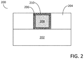
- FIG. 2 illustrates a schematic diagram of an exemplary device structure including a transition metal containing film deposited according to the embodiments of the disclosure
- FIG. 3 illustrates an example of transition metal halide compound utilized in the cyclical deposition processes of the disclosure
- FIG. 4 illustrates a schematic diagram of an exemplary vapor deposition apparatus according to the embodiments of the disclosure.
- cyclic deposition may refer to the sequential introduction of precursors (reactants) into a reaction chamber to deposit a film over a substrate and includes deposition techniques such as atomic layer deposition and cyclical chemical vapor deposition.
- cyclical chemical vapor deposition may refer to any process wherein a substrate is sequentially exposed to two or more volatile precursors, which react and/or decompose on a substrate to produce a desired deposition.
- substrate may refer to any underlying material or materials that may be used, or upon which, a device, a circuit or a film may be formed.
- the term “atomic layer deposition” may refer to a vapor deposition process in which deposition cycles, preferably a plurality of consecutive deposition cycles, are conducted in a process chamber.
- a deposition surface e.g., a substrate surface or a previously deposited underlying surface such as material from a previous ALD cycle
- a reactant e.g., another precursor or reaction gas
- this reactant is capable of further reaction with the precursor.
- purging steps may also be utilized during each cycle to remove excess precursor from the process chamber and/or remove excess reactant and/or reaction byproducts from the process chamber after conversion of the chemisorbed precursor.
- atomic layer deposition is also meant to include processes designated by related terms such as, “chemical vapor atomic layer deposition”, “atomic layer epitaxy” (ALE), molecular beam epitaxy (MBE), gas source MBE, or organometallic MBE, and chemical beam epitaxy when performed with alternating pulses of precursor composition(s), reactive gas, and purge (e.g., inert carrier) gas.
- film may refer to any continuous or non-continuous structures and material deposited by the methods disclosed herein.
- film could include 2D materials, nanorods, nanotubes, or nanoparticles or even partial or full molecular layers or partial or full atomic layers or clusters of atoms and/or molecules.
- Finm may comprise material or a layer with pinholes, but still be at least partially continuous.
- transition metal containing film may refer to a film containing a transition metal species, including, but not limited to, elemental transition metals, transition metal oxides, transition metal nitrides, transition metal silicides, transition metal selenides, transition metal phosphides, transition metal borides, and mixtures thereof.
- transition metal containing film may refer to a film containing a transition metal species as well as containing carbon and/or hydrogen.
- the present disclosure includes methods for forming transition metal containing films on a substrate and particular methods for the cyclical deposition of a transition metal containing film on a substrate.
- the embodiments of the disclosure may include methods for the cyclical deposition of transition metal containing films, such as, for example, copper containing films, nickel containing films, and particularly cobalt containing films.
- cyclical deposition methods may be utilized to deposit cobalt containing films, such as, for example, elemental cobalt, cobalt oxides, cobalt nitrides, cobalt silicides, cobalt phosphides, cobalt selenides, or cobalt borides.
- cobalt metallic films may be important in such applications as liner layers and capping layers to suppress the electromigration of copper interconnect materials into surrounding dielectric materials. Indeed, as device feature sizes decrease in advanced technology nodes, cobalt metallic films may be utilized as the interconnection material, replacing the commonly utilized copper interconnects. Cobalt metallic films may also be of interest in giant magnetoresistance applications and magnetic memory applications.
- cobalt thin films may also be deposited onto silicon gate contacts in integrated circuits to form a cobalt silicide upon annealing.
- the oxides of cobalt may have applications in emerging energy related technologies, such as, for example, lithium-ion batteries and electrochemical water oxidation, as well as being utilized as a catalysis material.
- Deposition of elemental cobalt and cobalt containing films has been typically achieved utilizing sputtering techniques, as well as CVD methods employing metalorganic precursors.
- sputtering techniques as well as CVD methods employing metalorganic precursors.
- known methods for the deposition of cobalt containing films may be unsuitable for advanced technology nodes due to their inherent non-conformality.
- Cyclical deposition methods such as atomic layer deposition, are characteristically conformal deposition methods and are highly suitable for the deposition of conformal transition metal containing films over three-dimensional structure including high aspect ratio features. Accordingly, cyclical deposition methods for the deposition of transition metal containing films, and particular for the deposition of cobalt containing films are highly desirable.
- cyclical deposition methods for cobalt containing films has been hindered by the lack of suitable chemical precursors and cost effective chemical precursors.
- the cyclical deposition of cobalt containing films utilizing known chemical precursors may require undesirable high temperature deposition processes, e.g., above 300° C.
- Plasma enhanced atomic layer deposition processes may be utilized for the deposition of cobalt containing films at lower deposition temperatures but the utilization of a plasma based process may be undesirable in some device applications due to the potential damage of the underlying semiconductor device structures from the high energy plasma reactive species.
- chemical precursors suitable for the deposition of transition metal containing films are desirable and particular chemical precursor for the deposition of cobalt containing films by cyclical deposition processes.
- methods and related apparatus are needed for supplying a chemical precursor to a suitable vapor deposition system, such as, for example, an atomic layer deposition apparatus.
- the embodiments of the disclosure may comprise a method of forming a transition metal containing film on a substrate by a cyclical deposition process.
- the method may comprise: contacting the substrate with a first vapor phase reactant comprising a transition metal halide compound comprising a bidentate nitrogen containing adduct ligand; and contacting the substrate with a second vapor phase reactant.
- a transition metal containing layer may be deposited by a cyclical deposition process utilizing a transition metal halide compound as the metal precursor.
- a non-limiting example embodiment of a cyclical deposition process may include atomic layer deposition (ALD), wherein ALD is based on typically self-limiting reactions, whereby sequential and alternating pulses of reactants are used to deposit about one atomic (or molecular) monolayer of material per deposition cycle.
- ALD atomic layer deposition
- the deposition conditions and precursors are typically selected to provide self-saturating reactions, such that an adsorbed layer of one reactant leaves a surface termination that is non-reactive with the gas phase reactants of the same reactant.
- each cycle of alternated pulses typically leaves no more than about one monolayer of the desired material.
- the skilled artisan will recognize that in one or more ALD cycles more than one monolayer of material may be deposited, for example if some gas phase reactions occur despite the alternating nature of the process.
- one deposition cycle may comprise, contacting the substrate to a first reactant, removing any unreacted first reactant and reaction byproducts from the reaction space, and contacting the substrate to a second reactant, followed by a second removal step.
- the first reactant may comprise a transition metal halide compound (“the metal precursor”) and the second reactant may comprise at least one of an oxygen precursor, a nitrogen precursor, a silicon precursor, a sulfur precursor, a selenium precursor, a phosphorous precursor, a boron precursor, or a reducing agent.
- Precursors may be separated by inert gases, such as argon (Ar) or nitrogen (N 2 ), to prevent gas-phase reactions between reactants and enable self-saturating surface reactions.
- the substrate may be moved to separately contact a first vapor phase reactant and a second vapor phase reactant. Because the reactions self-saturate, strict temperature control of the substrates and precise dosage control of the precursors may not be required.
- the substrate temperature is preferably such that an incident gas species does not condense into monolayers nor decompose on the surface.
- Surplus chemicals and reaction byproducts, if any are removed from the substrate surface, such as by purging the reaction space or by moving the substrate, before the substrate is contacted with the next reactive chemical. Undesired gaseous molecules can be effectively expelled from a reaction space with the help of an inert purging gas.
- a vacuum pump may be used to assist in the purging.
- Reactors capable of being used to deposit transition metal containing films can be used for the deposition.
- Such reactors include ALD reactors, as well as CVD reactors equipped with appropriate equipment and means for providing the precursors.
- a showerhead reactor may be used.
- cross-flow, batch, minibatch, or spatial ALD reactors may be used.
- reactors examples include commercially available single substrate (or single wafer) deposition equipment such as Pulsar® reactors (such as the Pulsar® 2000 and the Pulsar® 3000 and Pulsar® XP ALD), and EmerALD® XP and the EmerALD® reactors, available from ASM America, Inc. of Phoenix, Ariz. and ASM Europe B.V., Almere, Netherlands.
- Other commercially available reactors include those from ASM Japan K.K. (Tokyo, Japan) under the tradename Eagle® XP and XP8.
- the reactor is a spatial ALD reactor, in which the substrates moves or rotates during processing.
- a batch reactor may be used. Suitable batch reactors include, but are not limited to, Advance® 400 Series reactors commercially available from and ASM Europe B.V. (Almere, Netherlands) under the trade names A400 and A412 PLUS. In some embodiments the wafers rotate during processing. In other embodiments, the batch reactor comprises a minibatch reactor configured to accommodate 10 or fewer wafers, 8 or fewer wafers, 6 or fewer wafers, 4 or fewer wafers, or 2 or fewer wafers. In some embodiments in which a batch reactor is used, wafer-to-wafer non-uniformity is less than 3% (1sigma), less than 2%, less than 1% or even less than 0.5%.
- the deposition processes described herein can optionally be carried out in a reactor or a reaction chamber connected to a cluster tool.
- a cluster tool because each reaction chamber is dedicated to one type of process, the temperature of the reaction chamber in each module can be kept constant, which improves the throughput compared to a reactor in which the substrate is heated up to the process temperature before each run. Additionally, in a cluster tool it is possible to reduce the time to pump the reaction chamber to the desired process pressure levels between substrates.
- the deposition process may be performed in a cluster tool comprising multiple reaction chambers, wherein each individual reaction chamber may be utilized to expose the substrate to an individual precursor gas and the substrate may be transferred between the different reaction chambers for exposure to multiple precursors gases, the transfer of the substrate being performed under a controlled ambient to prevent oxidation/contamination of the substrate.
- the deposition process may be performed in a cluster tool comprising multiple reaction chambers, wherein each individual reaction chamber may be configured to heat the substrate to a different deposition temperature.
- a stand-alone reactor can be equipped with a load-lock. In that case, it is not necessary to cool down the reaction space between each run.
- a deposition process for depositing a transition metal containing film may comprise a plurality of deposition cycles, for example ALD cycles, or cyclical CVD cycles.
- the cyclical deposition processes are used to form transition metal containing films on a substrate and the cyclical deposition process may be an ALD type process.
- the cyclical deposition may be a hybrid ALD/CVD or cyclical CVD process.
- the growth rate of the ALD process may be low compared with a CVD process.
- One approach to increase the growth rate may be that of operating at a higher substrate temperature than that typically employed in an ALD process, resulting in a chemical vapor deposition process, but still taking advantage of the sequential introduction of precursors, such a process may be referred to as cyclical CVD.
- ALD processes may be used to deposit a transition metal containing film on a substrate, such as a partially fabricated semiconductor device structure.
- each ALD cycle comprises two distinct deposition steps or phases.
- the metal phase the substrate surface on which deposition is desired is contacted with a first vapor phase reactant comprising a metal precursor which chemisorbs onto the substrate surface, forming no more than about one monolayer of reactant species on the surface of the substrate.
- the substrate surface on which deposition is desired is contacted with a second vapor phase reactant comprising at least one of an oxygen precursor, a nitrogen precursor, a silicon precursor, a sulfur precursor, a selenium precursor, a phosphorous precursor, a boron precursor, or a reducing agent, wherein the second vapor phase reactant may react with transition metal species on a surface of the substrate to form a transition metal containing film on the substrate, such as, for example, an elemental transition metal, a transition metal oxide, a transition metal nitride, a transition metal silicide, a transition metal selenide, a transition metal phosphide, a transition metal boride, and mixtures thereof, as well transition metal containing films further comprising carbon and/or hydrogen.
- a second vapor phase reactant comprising at least one of an oxygen precursor, a nitrogen precursor, a silicon precursor, a sulfur precursor, a selenium precursor, a phosphorous precursor, a boron precursor, or a reducing agent
- the first vapor phase reactant may comprise a metal containing precursor, also referred to here as the “metal compound”.
- the first vapor phase reactant may comprise a transition metal compound with an adduct forming ligand.
- the first vapor phase reactant may comprise a transition metal compound.
- the first vapor phase reactant may comprise a transition metal halide compound.
- the first vapor phase reactant may comprise a transition metal compound with an adduct forming ligand, such as monodentate, bidentate, or multidentate adduct forming ligand.
- the first vapor phase reactant may comprise a transition metal halide compound with adduct forming ligand, such as monodentate, bidentate, or multidentate adduct forming ligand.
- the first vapor phase reactant may comprise a transition metal compound with adduct forming ligand comprising nitrogen, such as monodentate, bidentate, or multidentate adduct forming ligand comprising nitrogen.
- the first vapor phase reactant may comprise a transition metal compound with adduct forming ligand comprising phosphorous, oxygen, or sulfur, such as monodentate, bidentate, or multidentate adduct forming ligand comprising phosphorous, oxygen or sulfur.
- the transition metal halide compound may comprise a transition metal chloride, a transition metal iodide, a transition metal fluoride, or a transition metal bromide.
- the transition metal halide compound may comprise a transition metal species, including, but not limited to, at least one of cobalt, nickel, or copper.
- the transition metal halide compound may comprise at least one of a cobalt chloride, a nickel chloride, or a copper chloride.
- the transition metal halide compound may comprise a bidentate nitrogen containing adduct forming ligand.
- the transition metal halide compound may comprise an adduct forming ligand including two nitrogen atoms, wherein each of the nitrogen atoms are bonded to at least one carbon atom.
- the transition metal halide compound comprises one or more nitrogen atoms bonded to a central transition metal atom thereby forming a metal complex.
- the first vapor phase reactant may comprise a transition metal compound having the formula (I): (adduct) n -M-X a (I)
- each of the “adducts” is an adduct forming ligand and can be independently selected to be a mono-, a bi-, or a multidentate adduct forming ligand or mixtures thereof: n is from 1 to 4 in case of monodentate forming ligand, n is from 1 to 2 in case of bi- or multidentate adduct forming ligand; M is a transition metal, such as, for example, cobalt (Co), copper (Cu), or nickel (Ni); wherein each of X a is another ligand, and can be independently selected to be a halide or other ligand; wherein a is from 1 to 4, and some instances a is 2.
- the adduct forming ligand in the transition metal compound may comprise a monodentate, bidentate, or multidentate adduct forming ligand which coordinates to the transition metal atom, of the transition metal compound, through at least one of a nitrogen atom, a phosphorous atom, an oxygen atom, or a sulfur atom.
- the adduct forming ligand in the transition metal compound may comprise a cyclic adduct ligand.
- the adduct forming ligand in the transition metal compound may comprise mono, di-, or polyamines.
- the adduct forming ligand in the transition metal compound may comprise mono-, di-, or polyethers. In some embodiments, the adduct forming ligand in the transition metal compound may comprise mono-, di-, or polyphosphines. In some embodiments, the adduct forming ligand in the transition metal compound may comprise carbon and/or in addition to the nitrogen, oxygen, phosphorous, or sulfur in the adduct forming ligand.
- the adduct forming ligand in the transition metal compound may comprise one monodentate adduct forming ligand. In some embodiments of the disclosure, the adduct forming ligand in the transition metal compound may comprise two monodentate adduct forming ligands. In some embodiments of the disclosure, the adduct forming ligand in the transition metal compound may comprise three monodentate adduct forming ligand. In some embodiments of the disclosure, the adduct forming ligand in the transition metal compound may comprise four monodentate adduct forming ligands.
- the adduct forming ligand in the transition metal compound may comprise one bidentate adduct forming ligand. In some embodiments of the disclosure, the adduct forming ligand in the transition metal compound may comprise two bidentate adduct forming ligands. In some embodiments of the disclosure, the adduct forming ligand in the transition metal compound may comprise one multidentate adduct forming ligand. In some embodiments of the disclosure, the adduct forming ligand in the transition metal compound may comprise two multidentate adduct forming ligands.
- the adduct forming ligand comprises nitrogen, such as an amine, a diamine, or a polyamine adduct forming ligand.
- the transition metal compound may comprise at least one of, triethylamine (TEA), N,N,N′,N′-tetramethyl-1,2-ethylenediamine (CAS: 110-18-9) (TMEDA), N,N,N′,N′-Tetraethylethylenediamine (CAS: 150-77-6) (TEEDA), N,N′-diethyl-1,2-ethylenediamine (CAS: 111-74-0) (DEEDA), N,N′-diisopropylethylenediamine (CAS: 4013-94-9), N,N,N′,N′-tetramethyl-1,3-propanediamine (CAS: 110-95-2) (TMPDA), N,N,N′,N′-tetramethylmethanediamine (CAS: 51-80-9) (
- the adduct forming ligand comprises phosphorous, such as a phosphine, a diphosphine, or a polyphosphine adduct forming ligand.
- the transition metal compound may comprise at least one of, triethylphosphine (CAS: 554-70-1), trimethyl phosphite (CAS: 121-45-), 1,2-Bis(diethylphosphino)ethane (CAS: 6411-21-8) (BDEPE), or 1,3-Bis(diethylphosphino)propane (CAS: 29149-93-7).
- the adduct forming ligand comprises oxygen, such as an ether, a diether, or a polyether adduct forming ligand.
- the transition metal compound may comprise at least one of, 1,4-dioxane (CAS: 123-91-1), 1,2-dimethoxyethane (CAS: 110-71-4) (DME, monoglyme), Diethylene glycol dimethyl ether (CAS: 111-96-6) (diglyme), Triethylene glycol dimethyl ether (CAS: 112-49-2) (triglyme), or 1,4,7,10-Tetraoxacyclododecane (CAS: 294-93-9) (12-Crown-4).
- the adduct forming ligand may comprise a thiother, or mixed ether amine, such as, for example, at least one of 1,7-Diaza-12-crown-4: 1,7-Dioxa-4,10-diazacyclododecane (CAS: 294-92-8), or 1,2-bis(methylthio)ethane (CAS: 6628-18-8).
- a thiother, or mixed ether amine such as, for example, at least one of 1,7-Diaza-12-crown-4: 1,7-Dioxa-4,10-diazacyclododecane (CAS: 294-92-8), or 1,2-bis(methylthio)ethane (CAS: 6628-18-8).
- the transition metal halide compound may comprise cobalt chloride N,N,N′,N′-tetramethyl-1,2-ethylenediamine (CoCl 2 (TMEDA)). In some embodiments, the transition metal halide compound may comprise cobalt bromide tetramethylethylenediamine (CoBr 2 (TMEDA)). In some embodiments, the transition metal halide compound may comprise cobalt iodide tetramethylethylenediamine (CoI 2 (TMEDA)). In some embodiments, the transition metal halide compound may comprise cobalt chloride N,N,N′,N′-tetramethyl-1,3-propanediamine (CoCl 2 (TMPDA)).
- the transition metal halide compound may comprise at least one of cobalt chloride N,N,N′,N′-tetramethyl-1,2-ethylenediamine (CoCl 2 (TMEDA)), nickel chloride tetramethyl-1,3-propanediamine (NiCl 2 (TMPDA)), or nickel iodide tetramethyl-1,3-propanediamine (NiI 2 (TMPDA)).
- TMEDA cobalt chloride N,N,N′,N′-tetramethyl-1,2-ethylenediamine
- NiCl 2 TMPDA
- NiI 2 nickel iodide tetramethyl-1,3-propanediamine
- contacting the substrate with a first vapor phase reactant comprising a transition metal halide compound may comprise exposing, i.e., contacting, the substrate to the transition metal halide compound for a time period of between about 0.01 seconds and about 60 seconds, between about 0.05 seconds and about 10 seconds, or between about 0.1 seconds and about 5.0 seconds.
- the flow rate of the transition metal halide compound may be less than 2000 sccm, or less than 500 sccm, or even less than 100 sccm.
- the flow rate of the transition metal halide compound may range from about 1 to 2000 sccm, from about 5 to 1000 sccm, or from about 10 to about 500 sccm.
- Excess transition metal halide compound and reaction byproducts may be removed from the surface, e.g., by pumping with an inert gas.
- the methods may comprise a purge cycle wherein the substrate surface is purged for a time period of less than approximately 2.0 seconds.
- Excess transition metal halide compound and any reaction byproducts may be removed with the aid of a vacuum, generated by a pumping system, in fluid communication with the reaction chamber.
- the substrate may be contacted with a second vapor phase reactant comprising at least one of an oxygen precursor, a nitrogen precursor, a silicon precursor, a sulfur precursor, a selenium precursor, a phosphorous precursor, a boron precursor, or a reducing agent.
- the second vapor phase reactant may comprise an oxygen precursor and the transition metal containing film deposited by the cyclical deposition methods disclosed herein may comprise a transition metal oxide.
- the second vapor phase reactant may comprise a reducing agent, described in greater detail below, and the transition metal containing film deposited by the cyclical deposition methods disclosed here may comprise an elemental transition metal.
- the second vapor phase reactant may comprise a nitrogen precursor and the transition metal containing film deposited by the cyclical deposition methods disclosed herein may comprise a transition metal nitride.
- the second vapor phase reactant may comprise a silicon precursor and the transition metal containing film deposited by the cyclical deposition methods disclosed herein may comprise a transition metal silicide.
- the second vapor phase reactant may comprise a sulfur precursor and the transition metal containing film deposited by the cyclical deposition methods disclosed herein may comprise a transition metal sulfide.
- the second vapor phase reactant may comprise a selenium precursor and the transition metal containing film deposited by the cyclical deposition methods disclosed herein may comprise a transition metal selenide.
- the second vapor phase reactant may comprise a phosphorous precursor and the transition metal containing film deposited by the cyclical deposition methods disclosed herein may comprise a transition metal phosphide.
- the second vapor phase reactant may comprise a boron precursor and the transition metal containing film deposited by the cyclical deposition methods disclosed herein may comprise a transition metal boride.
- the oxygen precursor may comprise at least one of ozone (O 3 ), molecular oxygen (O 2 ), oxygen atoms (O), an oxygen plasma, oxygen radicals, oxygen excited species, water (H 2 O), or hydrogen peroxide (H 2 O 2 ).
- the nitrogen precursor may comprise at least one of ammonia (NH 3 ), hydrazine (N 2 H 4 ), triazane (N 3 H 5 ), tertbutylhydrazine (C 4 H 9 N 2 H 3 ), methylhydrazine (CH 3 NHNH 2 ), dimethylhydrazine ((CH 3 ) 2 N 2 H 2 ), or a nitrogen plasma or nitrogen plasma comprising hydrogen.
- the second vapor phase reactant may comprise a hydrocarbon substituted hydrazine precursor.
- substituted hydrazine phase the substrate is contacted with a second vapor phase reactant comprising a hydrocarbon substituted hydrazine precursor.
- methods may further comprise selecting the substituted hydrazine to comprise an alkyl group with at least four (4) carbon atoms, wherein “alkyl group” refers to a saturated or unsaturated hydrocarbon chain of at least four (4) carbon atoms in length, such as, but not limited to, butyl, pentyl, hexyl, heptyl and octyl and isomers thereof, such as n-, iso-, sec- and tert-isomers of those.
- the alkyl group may be straight chain or branched-chain and may embrace all structural isomer forms of the alkyl group. In some embodiments the alkyl chain might be substituted.
- the alkyl-hydrazine may comprise at least one hydrogen bonded to nitrogen. In some embodiments of the disclosure, the alkyl-hydrazine may comprise at least two hydrogens bonded to nitrogen. In some embodiments of the disclosure, the alkyl-hydrazine may comprise at least one hydrogen bonded to nitrogen and at least one alkyl chain bonded to nitrogen. In some embodiments of the disclosure, the second reactant may comprise an alkyl-hydrazine and may further comprise one or more of tertbutylhydrazine (C 4 H 9 N 2 H 3 ), dimethylhydrazine or diethylhydrazine. In some embodiments of the disclosure, the substituted hydrazine has at least one hydrocarbon group attached to nitrogen.
- the substituted hydrazine has at least two hydrocarbon groups attached to nitrogen. In some embodiments of the disclosure, the substituted hydrazine has at least three hydrocarbon groups attached to nitrogen. In some embodiments of the disclosure, the substituted hydrazine has at least one C1-C3 hydrocarbon group attached to nitrogen. In some embodiments of the disclosure, the substituted hydrazine has at least one C4-C10 hydrocarbon group attached to nitrogen. In some embodiments of the disclosure, the substituted hydrazine has linear, branched or cyclic or aromatic hydrocarbon group attached to nitrogen. In some embodiments of the disclosure the substituted hydrazine comprises substituted hydrocarbon group attached to nitrogen.
- the substituted hydrazine has the following formula II: R I R II —N—NR III R IV , (II)
- R 1 can be selected from hydrocarbon group, such as linear, branched, cyclic, aromatic or substituted hydrocarbon group and each of the R II , R III , R IV groups can be independently selected to be hydrogen or hydrocarbon groups, such as linear, branched, cyclic, aromatic or substituted hydrocarbon group.
- each of the R I , R II , R III , R IV can be C1-C10 hydrocarbon, C1-C3 hydrocarbon, C4-C10 hydrocarbon or hydrogen, such as linear, branched, cyclic, aromatic or substituted hydrocarbon group.
- at least one of the R I , R II , R III , R IV groups comprises aromatic group such as phenyl group.
- At least one of the R I , R II , R III , R IV groups comprises methyl, ethyl, n-propyl, i-propyl, n-butyl, i-butyl, s-butyl, tertbutyl group or phenyl group. In some embodiments at least two of the each R I , R II , R III , R IV groups can be independently selected to comprise methyl, ethyl, n-propyl, i-propyl, n-butyl, i-butyl, s-butyl, tertbutyl group or phenyl group. In some embodiments R II , R III and R IV groups are hydrogen.
- At least two one of the R II , R III , R IV groups are hydrogen. In some embodiments at least one of the R II , R III , R IV groups are hydrogen. In some embodiments all of the R II , R III , R IV groups are hydrocarbons.
- the silicon precursor may comprise at least one of silane (SiH 4 ), disilane (Si 2 H 6 ), trisilane (Si 3 H 8 ), tetrasilane (Si 4 H 10 ), isopentasilane (Si 5 H 12 ), or neopentasilane (Si 5 H 12 ).
- the silicon precursor may comprise a C1-C4 alkylsilane.
- the silicon precursor may comprise a precursor from silane family.
- the boron precursor may comprise at least one of borane (BH 3 ), diborane (B 2 H 6 ) or other boranes, such as decaborane (B 10 H 14 ).
- the hydrogen precursor may comprise at least one of H 2 , H atoms, H-ions, H-plasma or H-radicals.
- the second vapor phase reactant comprises a phosphorus precursor, a sulfur precursor, or a selenide precursor.
- the sulfur precursor comprises hydrogen and sulfur.
- the sulfur precursor is an alkylsulfur compound.
- the second reactant comprises one or more of elemental sulfur, H 2 S, (CH 3 ) 2 S, (NH 4 ) 2 S, ((CH 3 ) 2 SO), and H 2 S 2 .
- the selenium precursor is an alkylselenium compound.
- the second reactant comprises one or more of elemental selenium, H 2 Se, (CH 3 ) 2 Se and H 2 Se 2 .
- the selenium precursor comprises hydrogen and selenium.
- the second reactant may comprise alkylsilylcompounds of Te, Sb, Se, such as (Me3Si)2Te, (Me3Si)2Se or (Me3Si)3Sb.
- the phosphorus precursor is an alkylphosphorus compound.
- the second reactant comprises one or more of elemental phosphorus, PH 3 or alkylphosphines, such as methylphoshpine.
- the phosphorus precursor comprises hydrogen and phosphorus.
- the second vapor phase reactant comprises an organic precursor, such as a reducing agent, for example, alcohols, aldehydes or carboxylic acids or other organic compounds may be utilized, for example organic compounds not having metals or semimetals, but comprising —OH group.
- Alcohols can be primary alcohols, secondary alcohols, tertiary alcohols, polyhydroxy alcohols, cyclic alcohols, aromatic alcohols, and other derivatives of alcohols.
- Primary alcohols have an —OH group attached to a carbon atom which is bonded to another carbon atom, in particular primary alcohols according to the general formula (III): R1-OH (III)
- R1 is a linear or branched C1-C20 alkyl or alkenyl groups, such as methyl, ethyl, propyl, butyl, pentyl or hexyl.
- primary alcohols include methanol, ethanol, propanol, butanol, 2-methyl propanol and 2-methyl butanol.
- Secondary alcohols have an —OH group attached to a carbon atom that is bonded to two other carbon atoms.
- secondary alcohols have the general formula (IV):
- each R1 is selected independently from the group of linear or branched C1-C20 alkyl and alkenyl groups, such as methyl, ethyl, propyl, butyl, pentyl or hexyl.
- alkenyl groups such as methyl, ethyl, propyl, butyl, pentyl or hexyl.
- secondary alcohols include 2-propanol and 2-butanol.
- Tertiary alcohols have an —OH group attached to a carbon atom that is bonded to three other carbon atoms.
- tertiary alcohols have the general formula (V):
- each R1 is selected independently from the group of linear or branched C1-C20 alkyl and alkenyl groups, such as methyl, ethyl, propyl, butyl, pentyl or hexyl.
- alkenyl groups such as methyl, ethyl, propyl, butyl, pentyl or hexyl.
- An example of a tertiary alcohol is tert-butanol.
- Polyhydroxy alcohols such as diols and triols, have primary, secondary and/or tertiary alcohol groups as described above.
- Examples of polyhydroxy alcohol are ethylene glycol and glycerol.
- Cyclic alcohols have an —OH group attached to at least one carbon atom which is part of a ring of 1 to 10, such as 5-6 carbon atoms.
- Aromatic alcohols have at least one —OH group attached either to a benzene ring or to a carbon atom in a side chain.
- Organic precursors may comprise at least one aldehyde group (—CHO) are selected from the group consisting of compounds having the general formula (VI), alkanedial compounds having the general formula (VII), halogenated aldehydes and other derivatives of aldehydes.
- —CHO aldehyde group
- organic precursors are aldehydes having the general formula (VI): R3-CHO (VI)
- R3 is selected from the group consisting of hydrogen and linear or branched C1-C20 alkyl and alkenyl groups, such as methyl, ethyl, propyl, butyl, pentyl or hexyl. In some embodiments, R3 is selected from the group consisting of methyl or ethyl.
- Exemplary compounds, but not limited to, according to formula (VI) are formaldehyde, acetaldehyde and butyraldehyde.
- organic precursors are aldehydes having the general formula (VII): OHC—R4-CHO (VII)
- Organic precursors containing at least one —COOH group can be selected from the group consisting of compounds of the general formula (VIII), polycarboxylic acids, halogenated carboxylic acids and other derivatives of carboxylic acids.
- organic precursors are carboxylic acids having the general formula (VIII): R5-COOH (VIII)
- R5 is hydrogen or linear or branched C1-C20 alkyl or alkenyl group, such as methyl, ethyl, propyl, butyl, pentyl or hexyl, for example methyl or ethyl.
- R5 is a linear or branched C1-C3 alkyl or alkenyl group.
- Examples of compounds according to formula (VII) are formic acid, propanoic acid and acetic acid, in some embodiments formic acid (HCOOH).
- exposing, i.e., contacting, the substrate to the second vapor phase reactant comprise pulsing the second vapor phase reactant over the substrate for a time period of between 0.1 seconds and 2.0 seconds, or from about 0.01 seconds to about 10 seconds, or less than about 20 seconds, less than about 10 seconds or less than about 5 seconds.
- the flow rate of the second vapor phase reactant may be less than 50 sccm, or less than 25 sccm, or less than 15 sccm, or even less than 10 sccm.
- Excess second vapor phase reactant and reaction byproducts, if any, may be removed from the substrate surface, for example, by a purging gas pulse and/or vacuum generated by a pumping system.
- Purging gas is preferably any inert gas, such as, without limitation, argon (Ar), nitrogen (N 2 ), helium (He), or in some instances hydrogen (H 2 ) could be used.
- a phase is generally considered to immediately follow another phase if a purge (i.e., purging gas pulse) or other reactant removal step intervenes.
- a deposition cycle in which the substrate is alternatively contacted with the first vapor phase reactant (i.e., the metal halide compound) and the second vapor phase reactant (e.g., an oxygen precursor) may be repeated one or more times until a desired thickness of a transition metal containing film is deposited.
- the order of the contacting of the substrate with the first vapor phase reactant and the second vapor phase reactant may be such that the substrate is first contacted with the second vapor phase reactant followed by the first vapor phase reactant.
- the cyclical deposition process may comprise contacting the substrate with the first vapor phase reactant one or more times prior to contacting the substrate with the second vapor phase reactant one or more times and similarly may alternatively comprise contacting the substrate with the second vapor phase reactant one or more times prior to contacting the substrate with the first vapor phase reactant one or more times.
- some embodiments of the disclosure may comprise non-plasma reactants, e.g., the first and second vapor phase reactants are substantially free of ionized reactive species.
- the first and second vapor phase reactants are substantially free of ionized reactive species, excited species or radical species.
- both the first vapor phase reactant and the second vapor phase reactant may comprise non-plasma reactants to prevent ionization damage to the underlying substrate and the associated defects thereby created.
- the use of non-plasma reactants may be especially useful when the underlying substrate contains fragile fabricated, or least partially fabricated, semiconductor device structures as the high energy plasma species may damage and/or deteriorate device performance characteristics.
- exemplary cyclical deposition methods of the disclosure may comprise an additional process step comprising, contacting the substrate with a third vapor phase reactant comprising a reducing agent.
- the reducing agent may comprise at least one of hydrogen (H 2 ), a hydrogen (H 2 ) plasma, ammonia (NH 3 ), an ammonia (NH 3 ) plasma, hydrazine (N 2 H 4 ), silane (SiH 4 ), disilane (Si 2 H 6 ), trisilane (Si 3 H 8 ), germane (GeH 4 ), digermane (Ge 2 H 6 ), borane (BH 3 ), diborane (B 2 H 6 ), tertiary butyl hydrazine (C 4 H 12 N 2 , a selenium precursor, a boron precursor, a phosphorous precursor, a sulfur precursor, an organic precursor (e.g., alcohols, aldehydes, or carboxylic acids)
- the third vapor phase reactant comprising a reducing agent may be introduced into the reaction chamber and contact the substrate at a number process stages in an exemplary cyclical deposition method.
- the reducing agent may be introduced into the reaction chamber and contact the substrate separately from the first vapor phase reactant and separately from the second vapor phase reactant.
- the reducing agent may be introduced into the reaction chamber and contact the substrate prior to contacting the substrate with the first vapor phase reactant, after contacting the substrate with the first vapor phase reactant and prior to contacting the substrate with the second vapor phase reactant, and/or after contacting the substrate with the second vapor phase reactant.
- the reducing agent may be introduced into the reaction chamber and contact the substrate simultaneously with the first vapor phase reactant and/or simultaneously with the second vapor phase reactant.
- the reducing agent and the first vapor phase reactant may be co-flowed into the reaction chamber and simultaneously contact the substrate, and/or the reducing agent and the second vapor phase reactant may be co-flowed into the reaction chamber and simultaneously contact the substrate.
- the first vapor phase reactant may comprise a transition metal halide compound and the second vapor phase reactant may comprise an oxygen precursor.
- the cyclical deposition processes may deposit a transition metal oxide on the substrate.
- the first vapor phase reactant may comprise CoCl 2 (TMEDA)
- the second vapor phase reactant may comprise water (H 2 O)
- the film deposited on the substrate may comprise a cobalt oxide.
- the transition metal oxide may be further processed by exposing the transition metal oxide to a reducing agent.
- the transition metal oxide may be exposed to at least one reducing agent comprising, forming gas (H 2 +N 2 ), ammonia (NH 3 ), hydrazine (N 2 H 4 ), molecular hydrogen (H 2 ), hydrogen atoms (H), a hydrogen plasma, hydrogen radicals, hydrogen excited species, alcohols, aldehydes, carboxylic acids, boranes, or amines.
- at least one reducing agent comprising, forming gas (H 2 +N 2 ), ammonia (NH 3 ), hydrazine (N 2 H 4 ), molecular hydrogen (H 2 ), hydrogen atoms (H), a hydrogen plasma, hydrogen radicals, hydrogen excited species, alcohols, aldehydes, carboxylic acids, boranes, or amines.
- exposing the transition metal oxide to a reducing agent may reduce the transition metal oxide to an elemental transition metal.
- the cyclical deposition processes of the disclosure may be utilized to deposit a cobalt oxide film to a thickness of 50 nanometers and the cobalt oxide film may be exposed to 10% forming gas at a pressure of 1000 mbar and a temperature of approximately 250° C. to reduce the cobalt oxide film to elemental cobalt.
- the transition metal oxide may have a thickness of less than 500 nanometers, or less than 100 nanometers, or less than 50 nanometers, or less than 25 nanometers, or less than 20 nanometers, or less than 10 nanometers, or even less than 5 nanometers.
- the transition metal oxide may be exposed to a reducing agent for less than 5 hours, or less than 1 hour, or less than 30 minutes, or less than 15 minutes, or less than 10 minutes, or less than 5 minutes, or even less than 1 minutes.
- the transition metal oxide may be exposed to the reducing agent at a substrate temperature of less than 500° C., or less than 400° C., or less than 300° C., or less than 250° C., or less than 200° C., or even less than 150° C.
- the transition metal oxide may be exposed to the reducing agent in a reduced pressure atmosphere, wherein the pressure may be from about 0.001 mbar to about 10 bar, or from about 1 mbar to about 1000 mbar.
- cyclical deposition processes described herein, utilizing a first vapor phase reactant comprise a transition metal halide compound and a second vapor phase reactant to deposit a transition metal containing film may be performed in an ALD or CVD deposition system with a heated substrate.
- methods may comprise heating the substrate to temperature of between approximately 80° C. and approximately 150° C., or even heating the substrate to a temperature of between approximately 80° C. and approximately 120° C.
- the appropriate temperature window for any given cyclical deposition process such as, for an ALD reaction, will depend upon the surface termination and reactant species involved.
- the temperature varies depending on the precursors being used and is generally at or below about 700° C.
- the deposition temperature is generally at or above about 100° C. for vapor deposition processes, in some embodiments the deposition temperature is between about 100° C. and about 300° C., and in some embodiments the deposition temperature is between about 120° C. and about 200° C. In some embodiments the deposition temperature is less than about 500° C., or less than below about 400° C., or less than about 350° C., or below about 300° C. In some instances the deposition temperature can be below about 300° C., below about 200° C. or below about 100° C. In some instances the deposition temperature can be above about 20° C., above about 50° C. and above about 75° C. In some embodiments of the disclosure, the deposition temperature i.e., the temperature of the substrate during deposition is approximately 275° C.
- the growth rate of the transition metal containing film is from about 0.005 ⁇ /cycle to about 5 ⁇ /cycle, from about 0.01 ⁇ /cycle to about 2.0 ⁇ /cycle. In some embodiments the growth rate of the transition metal containing film is more than about 0.05 ⁇ /cycle, more than about 0.1 ⁇ /cycle, more than about 0.15 ⁇ /cycle, more than about 0.20 ⁇ /cycle, more than about 0.25 ⁇ /cycle, or more than about 0.3 ⁇ /cycle. In some embodiments the growth rate of the transition metal containing film is less than about 2.0 ⁇ /cycle, less than about 1.0 ⁇ /cycle, less than about 0.75 ⁇ /cycle, less than about 0.5 ⁇ /cycle, or less than about 0.2 ⁇ /cycle. In some embodiments of the disclosure, the growth rate of the transition metal containing film may be approximately 0.4 ⁇ /cycle.
- the embodiments of the disclosure may comprise a cyclical deposition which may be illustrated in more detail by exemplary cyclical deposition method 100 of FIG. 1 .
- the method 100 may begin with a process block 110 which comprises, providing at least one substrate into a reaction chamber and heating the substrate to the deposition temperature.
- the substrate may comprise one or more partially fabricated semiconductor device structures
- the reaction chamber may comprise an atomic layer deposition reaction chamber
- the substrate may be heated to a deposition temperature of approximately less than 275° C.
- the pressure within the reaction chamber may be controlled to provide a reduced atmosphere in the reaction chamber.
- the pressure within the reaction chamber during the cyclical deposition process may be less than 1000 mbar, or less than 100 mbar, or less than 10 mbar, or less than 5 mbar, or even, in some instances less than 1 mbar.
- the method 100 may continue with a process block 120 which comprises, contacting the substrate with a transition metal halide compound, for example, the substrate may be contacted with the transition metal halide compound for a time period of approximately 1 second.
- the transition metal compound may contact the substrate for a time period of between about 0.01 seconds and about 60 seconds, or between about 0.05 seconds and about 10 seconds, or between about 0.1 seconds and about 5 seconds.
- the flow rate of the transition metal precursor may be less than 2000 sccm, or less than 1000 sccm, or less than 500 sccm, or less than 200 sccm, or even less than 100 sccm.
- excess metal precursor and any reaction byproducts may be removed from the reaction chamber by a purge/pump process.
- the method 100 may continue with a process block 130 which comprises, contacting the substrate with a second vapor phase reactant, such as, for example, an oxygen precursor, a nitrogen precursor, a silicon precursor, a phosphorous precursor, a selenium precursor, a boron precursor, or a reducing agent.
- a second vapor phase reactant such as, for example, an oxygen precursor, a nitrogen precursor, a silicon precursor, a phosphorous precursor, a selenium precursor, a boron precursor, or a reducing agent.
- the second vapor phase reactant e.g., water
- the second vapor phase reactant may contact the substrate for a time period of between about 0.01 seconds and about 60 seconds, or between about 0.05 seconds and about 10 seconds, or between about 0.1 seconds and about 5.0 seconds.
- the flow rate of the second vapor phase reactant may be less than 2000 sccm, or less than 1000 sccm, or less than 500 sccm, or less than 200 sccm, or even less than 100 sccm.
- the excess second vapor phase reactant and any reaction byproducts may be removed from the reaction chamber by a purge/pump process.
- the exemplary cyclical deposition method 100 wherein the substrate is alternatively and sequentially contacted with the transition metal halide compound (process block 120 ) and contacted with the second vapor phase reactant (process block 130 ) may constitute one deposition cycle.
- the method of depositing a transition metal containing film may comprise repeating the deposition cycle one or more times.
- the method 100 may continue with a decision gate 140 which determines if the cyclical deposition method 100 continues or exits via a process block 150 .
- the decision gate 140 is determined based on the thickness of the transition metal containing film deposited, for example, if the thickness of the transition metal containing film is insufficient for the desired device structure, then the method 100 may return to the process block 120 and the processes of contacting the substrate with the transition metal halide compound and contacting the substrate with the second vapor phase reactant may be repeated one or more times. Once the transition metal containing film has been deposited to a desired thickness the method may exit via the process block 150 and the transition metal containing film and the underlying semiconductor structure may be subjected to additional processes to form one or more device structures.
- Films, or layers, comprising a transition metal deposited according to some of the embodiments described herein may be continuous thin films.
- the thin films comprising a transition metal deposited according to some of the embodiments described herein may be continuous at a thickness below approximately 100 nanometers, or below approximately 60 nanometers, or below approximately 50 nanometers, or below approximately 40 nanometers, or below approximately 30 nanometers, or below approximately 25 nanometers, or below approximately 20 nanometers, or below approximately 15 nanometers, or below approximately 10 nanometers, or below approximately 5 nanometers, or lower.
- the continuity referred to herein can be physically continuity or electrical continuity.
- the thickness at which a film may be physically continuous may not be the same as the thickness at which a film is electrically continuous, and the thickness at which a film may be electrically continuous may not be the same as the thickness at which a film is physically continuous.
- a transition metal containing film deposited according to some of the embodiments described herein may have a thickness from about 20 nanometers to about 100 nanometers. In some embodiments, a transition metal containing film deposited according to some of the embodiments described herein may have a thickness from about 20 nanometers to about 60 nanometers. In some embodiments, a transition metal containing film deposited according to some of the embodiments described herein may have a thickness greater than about 20 nanometers, or greater than about 30 nanometers, or greater than about 40 nanometers, or greater than about 50 nanometers, or greater than about 60 nanometers, or greater than about 100 nanometers, or greater than about 250 nanometers, or greater than about 500 nanometers, or greater.
- a transition metal containing film deposited according to some of the embodiments described herein may have a thickness of less than about 50 nanometers, less than about 30 nanometers, less than about 20 nanometers, less than about 15 nanometers, less than about 10 nanometers, less than about 5 nanometers, less than about 3 nanometers, less than about 2 nanometers, or even less than about 1 nanometer.
- the transition metal containing film may be deposited on a three-dimensional structure, e.g., a non-planar substrate comprising high aspect ratio features.
- the step coverage of the transition metal containing film may be equal to or greater than about 50%, or greater than about 80%, or greater than about 90%, or greater than about 95%, or greater than about 98%, or greater than about 99%, or greater in structures having aspect ratios (height/width) of more than about 2, more than about 5, more than about 10, more than about 25, more than about 50, or even more than about 100.
- the transition metal containing films deposited according to the embodiments of the current disclosure may comprise less than about 50 atomic % oxygen, less than about 25 atomic % oxygen, less than about 10 atomic % oxygen, less than about 5 atomic % oxygen, less than about 2 atomic % oxygen, or even less than about 1 atomic % oxygen.
- the transition metal containing films may comprise less than about 5 atomic % hydrogen, or less than about 2 atomic % of hydrogen, or less than about 1 atomic % of hydrogen, or even less than about 0.5 atomic % of hydrogen.
- the transition metal containing films may comprise less than about 5 atomic % carbon, or less than about 2 atomic % carbon, or less than about 1 atomic % carbon, or even less than about 0.5 atomic % of carbon. In yet further embodiments, the transition metal containing films may comprise less than about 5 atomic % halide species, or less than about 2 atomic % halide species, or less than about 1 atomic % halide species, or even less than about 0.5 atomic % of halide species. In some embodiments, the atomic % of the transition metal containing materials may be determined utilizing time of flight elastic recoil detection analysis (ToF-ERDA).
- ToF-ERDA time of flight elastic recoil detection analysis
- the cyclical deposition processes of the present disclosure may be utilized to deposit a transition metal oxide, such as, for example, a cobalt oxide.
- a transition metal oxide such as, for example, a cobalt oxide.
- Prior cobalt precursors utilized for cyclical deposition processes such as atomic layer deposition, have proven unreactive towards water (H 2 O) and therefore ozone (O 3 ) has commonly been utilized as the oxygen precursor.
- ozone for the cyclical deposition of a cobalt oxide typically leads to the formation of cobalt (II,III) oxide (Co 3 O 4 ) rather than cobalt (II) oxide (CoO).
- the cyclical deposition processes of the present disclosure may be utilized to deposit substantially cobalt (II) oxide (CoO) films, i.e., where the ratio of cobalt to oxygen is substantially equal to 1:1.
- the deposition temperature during the cyclical deposition process may affect the stoichiometry of the deposited films.
- the substrate temperature may influence the ratio of cobalt to oxygen (Co:O) in the deposited film. Therefore, as a non-limiting example embodiment of the disclosure, a cobalt oxide film may be deposited utilizing CoCl 2 (TMEDA) as the cobalt precursor and water (H 2 O) as the oxygen precursor. During such a cyclical deposition process the substrate temperature may be controlled at approximately 275° C., which may result in the deposition of cobalt (II) oxide (CoO) with a cobalt to oxygen ratio (Co:O) of approximately 1:1.
- TEDA CoCl 2
- H 2 O water
- the substrate temperature may be controlled at approximately 275° C., which may result in the deposition of cobalt (II) oxide (CoO) with a cobalt to oxygen ratio (Co:O) of approximately 1:1.
- transition metal containing films deposited by the cyclical deposition processes disclosed herein may be utilized in a variety of contexts, such as, for example, liner layers, capping layers, gap fill layers, trench fill layers, seed layers, contact layers/contact fill layers, electromigration improving layers, conducting interconnects in back-end-of-line (BEOL) applications, and in silicide form for semiconductor device contacts.
- the transition metal containing films of the current disclosure may utilized as an electrode, or at least a portion of an electrode, configured for providing electrical current to one or more device structures.
- the transition metal containing films of the current disclosure may be utilized in CMOS device applications as at least a portion of an electrode to one or more CMOS devices.
- a transition metal containing film such as, for example, cobalt may be utilized as a barrier material and/or a capping layer in a back-end-of-line (BEOL) metallization application, as illustrate in FIG. 2 .
- FIG. 2 illustrates a partially fabricated semiconductor device structure 200 comprising, a substrate 202 which may comprise partially fabricated and/or fabricated semiconductor device structures such as transistors and memory elements (not shown).
- the partially fabricated semiconductor device structure 200 may include a dielectric material 204 formed over the substrate 202 which may comprise a low dielectric constant material, i.e., a low-k dielectric, such as a silicon containing dielectric or a metal oxide.
- a trench may be formed in the dielectric material 204 and a barrier material 206 may disposed on the surface of the trench which prevents, or substantially prevents, the diffusion the metal interconnect material 208 into the surrounding dielectric material 204 .
- the barrier material 206 may comprise cobalt deposited by the cyclical deposition processes described herein.
- the cobalt film may have a thickness of less than 35 Angstroms, or 25 Angstroms, or even 15 Angstroms.
- the partially fabricated semiconductor structure 200 may also comprise a metal interconnect material 208 for electrical interconnecting a plurality of device structures disposed in substrate 202 .
- the metal interconnect material 208 may comprise one or more of copper, or cobalt.
- the partially fabricated semiconductor device structure 200 may also include a capping layer 210 disposed directly on the upper surface of the metal interconnect material 208 .
- the capping layer 210 may be utilized to prevent oxidation of the metal interconnect material 208 and importantly prevent the diffusion of the metal interconnect material 208 into additional dielectric materials formed over the partially fabricated semiconductor structure 200 in subsequent fabrication processes, i.e., for multi-level interconnect structures.
- the capping layer 210 may also comprise cobalt, with a thickness of less than 20 Angstroms, or less than 15 Angstroms, or even less than 10 Angstroms.
- the metal interconnect material 208 , the barrier material 206 , and the capping layer 210 may collectively form an electrode for the electrical interconnection of a plurality of semiconductor devices disposed in the substrate 202 .
- the embodiments of the disclosure may also be utilized for the synthesis of chemical precursors useful for vapor deposition processes, such as, for example, atomic layer deposition, chemical vapor deposition, and cyclical chemical vapor deposition.
- the embodiments of the disclosure may therefore comprise methods to synthesize a transition metal halide compound comprising an adduct forming ligand, as previously described herein, such as, for example, a transition metal halide comprising a bidentate nitrogen containing adduct ligand.
- the methods of the disclosure may be utilized to synthesize one or more of cobalt(II) chloride (TMEDA), nickel(II) chloride (TMEDA), or copper(II) chloride (TMEDA).
- the methods of the disclosure may be utilized to synthesize one or more of cobalt(II) iodide (TMEDA), nickel(II) iodide (TMEDA), or copper(II) iodide (TMEDA).
- the methods of the disclosure may be utilized to synthesize one or more of cobalt(II) bromide (TMEDA), nickel(II) bromide (TMEDA), or copper(II) bromide (TMEDA).
- the methods of the disclosure may be utilized to synthesize cobalt(II) chloride (TMPDA), nickel(II) chloride (TMPDA), and copper(II) chloride (TMPDA).
- the chemical precursor synthesis methods may be performed with all handling and manipulations carried out under rigorous exclusion of air and moisture using standard Schlenk techniques and an inert gas (e.g., N 2 or Ar) glove box.
- Anhydrous CoCl 2 (99%) and N,N,N′,N′-tetramethylethylenediamine (TMEDA) (99%) were utilized as reactants.
- dichloromethane (CH 2 Cl 2 ) was utilized as a suitable solvent, the process including deoxygenizing and drying the CH 2 Cl 2 over 4 ⁇ molecular sieves.
- an amount of CoCl 2 may be weighed and added to suitable vessel, much as a Schlenk bottle. An amount of the CH 2 Cl 2 may be added to the CoCl 2 . Subsequently, a stoichiometric amount of TMEDA maybe be dropwise added to the solution.
- the adduct forming ligand e.g., TMEDA
- the adduct forming ligand may added in excess of the halide compound, such as, for example, in an amount 2 times, or 5 times, or even 10 times greater than the amount of halide compound. The resulting suspension may be stirred for approximately 1 hour at room temperature.
- CoCl 2 6.00 g (46.211 mmol) of CoCl 2 may be weighed and added to a Schlenk bottle along with 100 ml of CH 2 Cl 2 . 5.37 g (46.211 mmol) of TMEDA may be added to the solution and stirred for 1 hour at room temperature. The resulting blue solution may be evaporated to dryness producing a blue colored raw product. The resulting raw product may be transferred to a sublimator wherein the product may be sublimed out at a temperature between approximately 150-200° C., thereby producing the CoCl 2 (TMEDA).
- TMEDA CoCl 2
- the resulting volatile transition metal halide compound e.g., CoCl 2 (TMEDA)
- TEDA may have a percentage impurity concentration of less than 5 at-%, or less than 2 at-%, or less than 1 at-%, or less than 0.1 at-% or even less than 0.01 at-%.
- the volatile transition metal halide compound may have a higher decomposition temperature compared with organic transition metal precursors.
- the transition metal halide compounds of the current disclosure may have a decomposition temperature greater than 150° C., or even greater than 200° C.
- a transition metal halide compound may be synthesized that may be utilized for the vapor deposition of transition metal containing films.
- the metal halide compound comprising an adduct forming ligand may be synthesized utilizing a one-step synthesis process comprising combining a transition metal halide compound and an adduct forming ligand at a temperature below approximately 50° C., or below approximately 30° C., or even below approximately 15° C., wherein the entire synthesis process may be completed in a time period of less than 5 hours, or less than 2 hours, or less than 1 hour, or even less than 30 minutes.
- the embodiments of the disclosure may also comprise vapor deposition apparatus including one or more precursor source vessels configured for containing a transition metal halide compound and for supplying a transition metal halide compound to a reaction chamber. Therefore, in some embodiments of the disclosure, a vapor deposition apparatus utilizing reactive volatile chemicals is provided.
- the apparatus may comprise: a reaction chamber; a substrate disposed within the reaction chamber, a precursor source vessel in fluid communication with the reaction chamber; and a transition metal halide compound comprising a bidentate nitrogen containing ligand disposed in the precursor source vessel.
- FIG. 4 schematically illustrates a vapor deposition apparatus 400 including a reaction chamber 400 .
- FIG. 4 is a simplified schematic version of the vapor deposition apparatus 400 and does not contain each and every element, i.e., such as each, but not limited to, valves, electrical connections, mass flow controllers, seals, and gas conduits, that may be utilized in the vapor deposition apparatus 400 of the current disclosure.
- the reaction chamber 402 may include a susceptor 404 configured for supporting a substrate 406 within the reaction chamber. Also disposed in the reaction chamber is a showerhead gas distributor 408 utilized for selectively exposing the substrate to various gases.
- a precursor source vessel 410 A may be in fluid communication, via conduits or other appropriate means 412 A, to the reaction chamber 402 and may further be coupled to a manifold, valve control systems, mass flow control systems, or mechanism to control a gaseous precursor originating the precursor source vessel 410 A.
- the precursor source vessel 410 A may be configured for storing a transition metal halide compound comprising a bidentate nitrogen containing ligand.
- the precursor source vessel 410 A may comprise a quartz material, which may be substantially chemically inert to the transition metal halide compound stored within the precursor source vessel 410 A.
- the precursor source vessel 410 A may be fabricated from a corrosion resistant metal or metal alloy, such as, for example, Hastelloy, Monel, or a combination thereof.
- the precursor source vessel 410 A may further comprise one or more heating units 414 configured for the heating the transition metal halide compound stored in the precursor source vessel 410 A.
- the one or more heating units 400 may be utilized to heat the transition metal halide compound to a temperature of approximately greater than 0° C., or approximately greater than 20° C., or approximately greater than 100° C., or approximately greater than 150° C., or approximately greater than 200° C., or approximately greater than 200° C., or approximately greater than 300° C., or even approximately greater than 400° C.
- the one or more heating units 414 may be configured to heat the transition metal halide compound stored in the precursor source vessel 410 A to temperature of approximately 170° C.
- the one or more heating units 414 associated with the precursor source vessel 410 A are configured for converting the transition metal halide compound from a solid to either a liquid or a gas. In some embodiments, the one or more heating units 414 associated with the precursor source vessel 410 A may be utilized to control the viscosity of the transition metal halide compound stored in the precursor storage vessel 410 A. In some embodiments, the one or more heating units 414 associated with the precursor source vessel 410 A may be configured for controlling the vapor pressure generated by the transition metal halide compound stored within the precursor source vessel.
- the transition metal halide compound may have a vapor pressure greater than 0.01 mbar at a temperature greater than 25° C., or greater than 50° C., or even greater than 100° C. In some embodiments of the disclosure, the transition metal halide compound may have a vapor pressure greater than 0.01 mbar at a temperature of less than 350° C., or less than 250° C., or less than 200° C., or even less than 150° C. In some embodiments of the disclosure, the transition metal halide compound may have a vapor pressure greater than 0.1 mbar at a temperature greater than 25° C., or even greater than 100° C.
- the transition metal halide compound may have a vapor pressure greater than 0.1 mbar at a temperature of less than 400° C., or less than 200° C., or even less than 100° C. In some embodiments of the disclosure, the transition metal halide compound may have a vapor pressure of greater than 1 mbar at a temperature of greater than 25° C., or even greater than 100° C. For example, the transition metal halide compound may be heated to a temperature greater than 150° C., generating a vapor pressure of greater than 0.001 mbar.
- the transition metal halide 416 stored within the precursor source vessel 410 A may comprise at least one of cobalt chloride (TMEDA), or nickel chloride (TMEDA). In some embodiments, the transition metal halide 416 stored within the precursor source vessel 410 A may comprise cobalt iodide (TMEDA. In some embodiments, the transition metal halide 416 stored within the precursor source vessel 410 A may comprise. In addition, in some embodiments, the transition metal halide 416 stored within the precursor source vessel 410 A may comprise cobalt chloride (TMPDA), and nickel chloride (TMPDA).
- TMEDA cobalt chloride
- TMEDA nickel chloride
- a vapor passageway 418 may be connected to the precursor source vessel 410 A such that one or more carrier gases may be transported from a carrier gas storage vessel (not shown) into the precursor source vessel via the vapor passageway 418 .
- a mass flow controller (not shown) may be placed on the vapor passageway 418 and disposed proximate to the precursor source vessel 410 A.
- a mass flow controller may be calibrated to control the mass flux of the carrier gas entering the precursor source vessel 410 A thereby allowing greater control over the subsequent flow of the transition metal halide compound vapor from out of the precursor source vessel 410 A to the reaction chamber 402 .
- the carrier gas (e.g., hydrogen, nitrogen, helium, argon, and mixtures thereof) may be flowed over an exposed surface of the transition metal halide compound 416 thereby picking up a portion of the vapor from the transition metal halide compound 416 and transporting the transition metal halide compound, along with the carrier gas, to the reaction chamber 402 .
- the carrier gas may be “bubbled” through the transition metal halide compound 416 , e.g., by optional vapor passageway 418 ′, thereby agitating and picking up a portion of the transition metal halide compound 416 and transporting the transition metal halide compound vapor to the reaction chamber 402 via gas conduit 412 A.
- the vapor deposition apparatus 400 may include additional precursor source vessel and one or more source vessel for inert purge gases.
- precursor source vessel 410 B may be configured to contain a second vapor phase reactant, such as, for example, one or more of an oxygen precursor, a nitrogen precursor, a sulfur precursor, a selenium precursor, a phosphorous precursor, a boron precursor, a silicon precursor, or a reducing agent.
- the second vapor phase reactant contained in the precursor source vessel 410 B may be transported to the reaction chamber 402 via gas conduit 412 B.
- the precursor source vessel 410 B may also have associated heaters 414 for controlling the temperature of the precursor stored within the precursor source vessel 410 B.
- source vessel 410 C may be utilized to contain an inert purge gas, such as, for example, without limitation, argon (Ar), nitrogen (N 2 ), or helium (He).
- an inert purge gas such as, for example, without limitation, argon (Ar), nitrogen (N 2 ), or helium (He).
- the vapor deposition apparatus 400 may further comprise a system operation and control mechanism 420 that provides electronic circuitry and mechanical components to selectively operate, valves, manifold, pumps, and other equipment associated with the vapor deposition apparatus 400 .
- a system operation and control mechanism 420 that provides electronic circuitry and mechanical components to selectively operate, valves, manifold, pumps, and other equipment associated with the vapor deposition apparatus 400 .
- Such circuitry and compounds operate to introduce precursors, purges gas, from the respective precursor source vessels, 410 A, 410 B and purge gas vessel 410 C.
- the system operation and control mechanism 420 may also control the timing of gas pulse sequences, the temperature of the substrate and reaction chamber, and the pressure of the reaction chamber and various other operations necessary to provide proper operation to the vapor deposition apparatus 400 .
- the operation and control mechanism 420 may include control software and electrically or pneumatically controlled valves to control the flow of precursors, reactants, and purge gases into and out of the reaction chamber 402 .
- the control system can include modules such as software and/or hardware components, e.g., a FPGA or ASIC, which performs certain tasks.
- a module can adventurously be configured to reside on the addressable storage medium of the control system and be configured to execute one or more processes.
- the vapor deposition apparatus 400 of FIG. 4 may be utilized for supplying a transition metal halide compound comprising a bidentate nitrogen containing adduct ligand to a vapor deposition tool.
- the method may comprise: providing a precursor source vessel configured for containing the transition metal halide compound; fluidly connecting the precursor source vessel to a reaction chamber; heating the transition metal halide compound contained in the precursor source vessel to a temperature greater than 150° C., generating a vapor pressure of the transition metal halide compound of at least 0.001 mbar; and supplying the transition metal halide compound to the reaction chamber.
- the transition metal halide compound may have a vapor pressure greater than 0.01 mbar at a temperature greater than 25° C., or greater than 50° C., or even greater than 100° C. In some embodiments of the disclosure, the transition metal halide compound may have a vapor pressure greater than 0.01 mbar at a temperature of less than 350° C., or less than 250° C., or less than 200° C., or even less than 150° C. In some embodiments of the disclosure, the transition metal halide compound may have a vapor pressure greater than 0.1 mbar at a temperature greater than 25° C., or even greater than 100° C.
- the transition metal halide compound may have a vapor pressure greater than 0.1 mbar at a temperature of less than 400° C., or less than 200° C., or even less than 100° C. In some embodiments of the disclosure, the transition metal halide compound may have a vapor pressure of greater than 1 mbar at a temperature of greater than 25° C., or even greater than 100° C.
- the transition metal halide compound may comprise at least one of cobalt chloride (TMEDA), or nickel chloride (TMPDA).
Landscapes
- Chemical & Material Sciences (AREA)
- General Chemical & Material Sciences (AREA)
- Chemical Kinetics & Catalysis (AREA)
- Engineering & Computer Science (AREA)
- Materials Engineering (AREA)
- Mechanical Engineering (AREA)
- Metallurgy (AREA)
- Organic Chemistry (AREA)
- Inorganic Chemistry (AREA)
- Chemical Vapour Deposition (AREA)
- Crystallography & Structural Chemistry (AREA)
- Internal Circuitry In Semiconductor Integrated Circuit Devices (AREA)
Priority Applications (11)
| Application Number | Priority Date | Filing Date | Title |
|---|---|---|---|
| US15/897,578 US10731249B2 (en) | 2018-02-15 | 2018-02-15 | Method of forming a transition metal containing film on a substrate by a cyclical deposition process, a method for supplying a transition metal halide compound to a reaction chamber, and related vapor deposition apparatus |
| TW108101159A TWI774907B (zh) | 2018-02-15 | 2019-01-11 | 藉由週期性沉積處理在基材上形成含過渡金屬薄膜的方法、供應過渡金屬鹵化物給反應腔的方法及相關的氣相沉積裝置 |
| TW111127939A TWI822206B (zh) | 2018-02-15 | 2019-01-11 | 一種利用反應揮發性化學物質的氣相沉積裝置 |
| CN202511440039.XA CN121451150A (zh) | 2018-02-15 | 2019-02-11 | 形成含过渡金属的膜的方法、供给方法及气相沉积装置 |
| JP2020543099A JP7391857B2 (ja) | 2018-02-15 | 2019-02-11 | 周期的堆積プロセスによって基材上に遷移金属含有膜を形成する方法、遷移金属ハロゲン化物化合物を反応チャンバーに供給する方法、及び関連蒸着装置 |
| PCT/IB2019/000127 WO2019158995A2 (fr) | 2018-02-15 | 2019-02-11 | Procédé de formation d'un film contenant un métal de transition sur un substrat par un procédé de dépôt cyclique, procédé d'introduction d'un composé d'halogénure de métal de transition dans une chambre de réaction, et appareil de dépôt en phase vapeur associé |
| KR1020207022406A KR102906695B1 (ko) | 2018-02-15 | 2019-02-11 | 주기적 증착 공정에 의해 기판 상에 전이 금속 함유 막을 형성하는 방법, 반응 챔버에 전이 금속 할라이드 화합물을 공급하는 방법, 및 관련 기상 증착 장치 |
| KR1020257043410A KR20260006089A (ko) | 2018-02-15 | 2019-02-11 | 주기적 증착 공정에 의해 기판 상에 전이 금속 함유 막을 형성하는 방법, 반응 챔버에 전이 금속 할라이드 화합물을 공급하는 방법, 및 관련 기상 증착 장치 |
| CN201980011788.7A CN111684105A (zh) | 2018-02-15 | 2019-02-11 | 通过循环沉积工艺在衬底上形成含过渡金属的膜的方法、向反应腔室供给过渡金属卤化物化合物的方法以及相关的气相沉积装置 |
| US16/927,509 US12173402B2 (en) | 2018-02-15 | 2020-07-13 | Method of forming a transition metal containing film on a substrate by a cyclical deposition process, a method for supplying a transition metal halide compound to a reaction chamber, and related vapor deposition apparatus |
| JP2023198228A JP7719843B2 (ja) | 2018-02-15 | 2023-11-22 | 周期的堆積プロセスによって基材上に遷移金属含有膜を形成する方法、遷移金属ハロゲン化物化合物を反応チャンバーに供給する方法、及び関連蒸着装置 |
Applications Claiming Priority (1)
| Application Number | Priority Date | Filing Date | Title |
|---|---|---|---|
| US15/897,578 US10731249B2 (en) | 2018-02-15 | 2018-02-15 | Method of forming a transition metal containing film on a substrate by a cyclical deposition process, a method for supplying a transition metal halide compound to a reaction chamber, and related vapor deposition apparatus |
Related Child Applications (1)
| Application Number | Title | Priority Date | Filing Date |
|---|---|---|---|
| US16/927,509 Division US12173402B2 (en) | 2018-02-15 | 2020-07-13 | Method of forming a transition metal containing film on a substrate by a cyclical deposition process, a method for supplying a transition metal halide compound to a reaction chamber, and related vapor deposition apparatus |
Publications (2)
| Publication Number | Publication Date |
|---|---|
| US20190249300A1 US20190249300A1 (en) | 2019-08-15 |
| US10731249B2 true US10731249B2 (en) | 2020-08-04 |
Family
ID=66397263
Family Applications (2)
| Application Number | Title | Priority Date | Filing Date |
|---|---|---|---|
| US15/897,578 Active 2038-05-04 US10731249B2 (en) | 2018-02-15 | 2018-02-15 | Method of forming a transition metal containing film on a substrate by a cyclical deposition process, a method for supplying a transition metal halide compound to a reaction chamber, and related vapor deposition apparatus |
| US16/927,509 Active 2040-06-12 US12173402B2 (en) | 2018-02-15 | 2020-07-13 | Method of forming a transition metal containing film on a substrate by a cyclical deposition process, a method for supplying a transition metal halide compound to a reaction chamber, and related vapor deposition apparatus |
Family Applications After (1)
| Application Number | Title | Priority Date | Filing Date |
|---|---|---|---|
| US16/927,509 Active 2040-06-12 US12173402B2 (en) | 2018-02-15 | 2020-07-13 | Method of forming a transition metal containing film on a substrate by a cyclical deposition process, a method for supplying a transition metal halide compound to a reaction chamber, and related vapor deposition apparatus |
Country Status (6)
| Country | Link |
|---|---|
| US (2) | US10731249B2 (fr) |
| JP (2) | JP7391857B2 (fr) |
| KR (2) | KR20260006089A (fr) |
| CN (2) | CN111684105A (fr) |
| TW (2) | TWI774907B (fr) |
| WO (1) | WO2019158995A2 (fr) |
Cited By (244)
| Publication number | Priority date | Publication date | Assignee | Title |
|---|---|---|---|---|
| US11274369B2 (en) | 2018-09-11 | 2022-03-15 | Asm Ip Holding B.V. | Thin film deposition method |
| US11286558B2 (en) | 2019-08-23 | 2022-03-29 | Asm Ip Holding B.V. | Methods for depositing a molybdenum nitride film on a surface of a substrate by a cyclical deposition process and related semiconductor device structures including a molybdenum nitride film |
| USD947913S1 (en) | 2019-05-17 | 2022-04-05 | Asm Ip Holding B.V. | Susceptor shaft |
| US11296189B2 (en) | 2018-06-21 | 2022-04-05 | Asm Ip Holding B.V. | Method for depositing a phosphorus doped silicon arsenide film and related semiconductor device structures |
| US11295980B2 (en) | 2017-08-30 | 2022-04-05 | Asm Ip Holding B.V. | Methods for depositing a molybdenum metal film over a dielectric surface of a substrate by a cyclical deposition process and related semiconductor device structures |
| US11306395B2 (en) | 2017-06-28 | 2022-04-19 | Asm Ip Holding B.V. | Methods for depositing a transition metal nitride film on a substrate by atomic layer deposition and related deposition apparatus |
| US11315794B2 (en) | 2019-10-21 | 2022-04-26 | Asm Ip Holding B.V. | Apparatus and methods for selectively etching films |
| US11339476B2 (en) | 2019-10-08 | 2022-05-24 | Asm Ip Holding B.V. | Substrate processing device having connection plates, substrate processing method |
| US11342216B2 (en) | 2019-02-20 | 2022-05-24 | Asm Ip Holding B.V. | Cyclical deposition method and apparatus for filling a recess formed within a substrate surface |
| US20220165566A1 (en) * | 2020-11-20 | 2022-05-26 | Applied Materials, Inc. | Conformal silicon-germanium film deposition |
| US11345999B2 (en) | 2019-06-06 | 2022-05-31 | Asm Ip Holding B.V. | Method of using a gas-phase reactor system including analyzing exhausted gas |
| US11355338B2 (en) | 2019-05-10 | 2022-06-07 | Asm Ip Holding B.V. | Method of depositing material onto a surface and structure formed according to the method |
| US11361990B2 (en) | 2018-05-28 | 2022-06-14 | Asm Ip Holding B.V. | Substrate processing method and device manufactured by using the same |
| US11378337B2 (en) | 2019-03-28 | 2022-07-05 | Asm Ip Holding B.V. | Door opener and substrate processing apparatus provided therewith |
| US11387120B2 (en) | 2017-09-28 | 2022-07-12 | Asm Ip Holding B.V. | Chemical dispensing apparatus and methods for dispensing a chemical to a reaction chamber |
| US11387106B2 (en) | 2018-02-14 | 2022-07-12 | Asm Ip Holding B.V. | Method for depositing a ruthenium-containing film on a substrate by a cyclical deposition process |
| US11390950B2 (en) | 2017-01-10 | 2022-07-19 | Asm Ip Holding B.V. | Reactor system and method to reduce residue buildup during a film deposition process |
| US11390946B2 (en) * | 2019-01-17 | 2022-07-19 | Asm Ip Holding B.V. | Methods of forming a transition metal containing film on a substrate by a cyclical deposition process |
| US11393690B2 (en) | 2018-01-19 | 2022-07-19 | Asm Ip Holding B.V. | Deposition method |
| US11390945B2 (en) | 2019-07-03 | 2022-07-19 | Asm Ip Holding B.V. | Temperature control assembly for substrate processing apparatus and method of using same |
| US11398382B2 (en) | 2018-03-27 | 2022-07-26 | Asm Ip Holding B.V. | Method of forming an electrode on a substrate and a semiconductor device structure including an electrode |
| US11396702B2 (en) | 2016-11-15 | 2022-07-26 | Asm Ip Holding B.V. | Gas supply unit and substrate processing apparatus including the gas supply unit |
| US11401605B2 (en) | 2019-11-26 | 2022-08-02 | Asm Ip Holding B.V. | Substrate processing apparatus |
| US11411088B2 (en) | 2018-11-16 | 2022-08-09 | Asm Ip Holding B.V. | Methods for forming a metal silicate film on a substrate in a reaction chamber and related semiconductor device structures |
| US11410851B2 (en) | 2017-02-15 | 2022-08-09 | Asm Ip Holding B.V. | Methods for forming a metallic film on a substrate by cyclical deposition and related semiconductor device structures |
| US11414760B2 (en) | 2018-10-08 | 2022-08-16 | Asm Ip Holding B.V. | Substrate support unit, thin film deposition apparatus including the same, and substrate processing apparatus including the same |
| US11417545B2 (en) | 2017-08-08 | 2022-08-16 | Asm Ip Holding B.V. | Radiation shield |
| US11424119B2 (en) | 2019-03-08 | 2022-08-23 | Asm Ip Holding B.V. | Method for selective deposition of silicon nitride layer and structure including selectively-deposited silicon nitride layer |
| US11430640B2 (en) | 2019-07-30 | 2022-08-30 | Asm Ip Holding B.V. | Substrate processing apparatus |
| US11430674B2 (en) | 2018-08-22 | 2022-08-30 | Asm Ip Holding B.V. | Sensor array, apparatus for dispensing a vapor phase reactant to a reaction chamber and related methods |
| US11437241B2 (en) | 2020-04-08 | 2022-09-06 | Asm Ip Holding B.V. | Apparatus and methods for selectively etching silicon oxide films |
| US11443926B2 (en) | 2019-07-30 | 2022-09-13 | Asm Ip Holding B.V. | Substrate processing apparatus |
| US11447864B2 (en) | 2019-04-19 | 2022-09-20 | Asm Ip Holding B.V. | Layer forming method and apparatus |
| US11447861B2 (en) | 2016-12-15 | 2022-09-20 | Asm Ip Holding B.V. | Sequential infiltration synthesis apparatus and a method of forming a patterned structure |
| US11450529B2 (en) | 2019-11-26 | 2022-09-20 | Asm Ip Holding B.V. | Methods for selectively forming a target film on a substrate comprising a first dielectric surface and a second metallic surface |
| USD965044S1 (en) | 2019-08-19 | 2022-09-27 | Asm Ip Holding B.V. | Susceptor shaft |
| US11453943B2 (en) | 2016-05-25 | 2022-09-27 | Asm Ip Holding B.V. | Method for forming carbon-containing silicon/metal oxide or nitride film by ALD using silicon precursor and hydrocarbon precursor |
| USD965524S1 (en) | 2019-08-19 | 2022-10-04 | Asm Ip Holding B.V. | Susceptor support |
| US11476109B2 (en) | 2019-06-11 | 2022-10-18 | Asm Ip Holding B.V. | Method of forming an electronic structure using reforming gas, system for performing the method, and structure formed using the method |
| US11473195B2 (en) | 2018-03-01 | 2022-10-18 | Asm Ip Holding B.V. | Semiconductor processing apparatus and a method for processing a substrate |
| US11482418B2 (en) | 2018-02-20 | 2022-10-25 | Asm Ip Holding B.V. | Substrate processing method and apparatus |
| US11482533B2 (en) | 2019-02-20 | 2022-10-25 | Asm Ip Holding B.V. | Apparatus and methods for plug fill deposition in 3-D NAND applications |
| US11482412B2 (en) | 2018-01-19 | 2022-10-25 | Asm Ip Holding B.V. | Method for depositing a gap-fill layer by plasma-assisted deposition |
| US11488819B2 (en) | 2018-12-04 | 2022-11-01 | Asm Ip Holding B.V. | Method of cleaning substrate processing apparatus |
| US11488854B2 (en) | 2020-03-11 | 2022-11-01 | Asm Ip Holding B.V. | Substrate handling device with adjustable joints |
| US11492703B2 (en) | 2018-06-27 | 2022-11-08 | Asm Ip Holding B.V. | Cyclic deposition methods for forming metal-containing material and films and structures including the metal-containing material |
| US11495459B2 (en) | 2019-09-04 | 2022-11-08 | Asm Ip Holding B.V. | Methods for selective deposition using a sacrificial capping layer |
| US11501968B2 (en) | 2019-11-15 | 2022-11-15 | Asm Ip Holding B.V. | Method for providing a semiconductor device with silicon filled gaps |
| US11501973B2 (en) | 2018-01-16 | 2022-11-15 | Asm Ip Holding B.V. | Method for depositing a material film on a substrate within a reaction chamber by a cyclical deposition process and related device structures |
| US11499222B2 (en) | 2018-06-27 | 2022-11-15 | Asm Ip Holding B.V. | Cyclic deposition methods for forming metal-containing material and films and structures including the metal-containing material |
| US11499226B2 (en) | 2018-11-02 | 2022-11-15 | Asm Ip Holding B.V. | Substrate supporting unit and a substrate processing device including the same |
| US11515188B2 (en) | 2019-05-16 | 2022-11-29 | Asm Ip Holding B.V. | Wafer boat handling device, vertical batch furnace and method |
| US11515187B2 (en) | 2020-05-01 | 2022-11-29 | Asm Ip Holding B.V. | Fast FOUP swapping with a FOUP handler |
| US11521851B2 (en) | 2020-02-03 | 2022-12-06 | Asm Ip Holding B.V. | Method of forming structures including a vanadium or indium layer |
| US11527403B2 (en) | 2019-12-19 | 2022-12-13 | Asm Ip Holding B.V. | Methods for filling a gap feature on a substrate surface and related semiconductor structures |
| US11532757B2 (en) | 2016-10-27 | 2022-12-20 | Asm Ip Holding B.V. | Deposition of charge trapping layers |
| US11530876B2 (en) | 2020-04-24 | 2022-12-20 | Asm Ip Holding B.V. | Vertical batch furnace assembly comprising a cooling gas supply |
| US11530483B2 (en) | 2018-06-21 | 2022-12-20 | Asm Ip Holding B.V. | Substrate processing system |
| US11551925B2 (en) | 2019-04-01 | 2023-01-10 | Asm Ip Holding B.V. | Method for manufacturing a semiconductor device |
| US11551912B2 (en) | 2020-01-20 | 2023-01-10 | Asm Ip Holding B.V. | Method of forming thin film and method of modifying surface of thin film |
| US11557474B2 (en) | 2019-07-29 | 2023-01-17 | Asm Ip Holding B.V. | Methods for selective deposition utilizing n-type dopants and/or alternative dopants to achieve high dopant incorporation |
| USD975665S1 (en) | 2019-05-17 | 2023-01-17 | Asm Ip Holding B.V. | Susceptor shaft |
| US11562901B2 (en) | 2019-09-25 | 2023-01-24 | Asm Ip Holding B.V. | Substrate processing method |
| US11572620B2 (en) | 2018-11-06 | 2023-02-07 | Asm Ip Holding B.V. | Methods for selectively depositing an amorphous silicon film on a substrate |
| US11581186B2 (en) | 2016-12-15 | 2023-02-14 | Asm Ip Holding B.V. | Sequential infiltration synthesis apparatus |
| US11587815B2 (en) | 2019-07-31 | 2023-02-21 | Asm Ip Holding B.V. | Vertical batch furnace assembly |
| US11587814B2 (en) | 2019-07-31 | 2023-02-21 | Asm Ip Holding B.V. | Vertical batch furnace assembly |
| US11587821B2 (en) | 2017-08-08 | 2023-02-21 | Asm Ip Holding B.V. | Substrate lift mechanism and reactor including same |
| US11594600B2 (en) | 2019-11-05 | 2023-02-28 | Asm Ip Holding B.V. | Structures with doped semiconductor layers and methods and systems for forming same |
| US11594450B2 (en) | 2019-08-22 | 2023-02-28 | Asm Ip Holding B.V. | Method for forming a structure with a hole |
| USD979506S1 (en) | 2019-08-22 | 2023-02-28 | Asm Ip Holding B.V. | Insulator |
| USD980813S1 (en) | 2021-05-11 | 2023-03-14 | Asm Ip Holding B.V. | Gas flow control plate for substrate processing apparatus |
| USD980814S1 (en) | 2021-05-11 | 2023-03-14 | Asm Ip Holding B.V. | Gas distributor for substrate processing apparatus |
| US11605528B2 (en) | 2019-07-09 | 2023-03-14 | Asm Ip Holding B.V. | Plasma device using coaxial waveguide, and substrate treatment method |
| US11610774B2 (en) | 2019-10-02 | 2023-03-21 | Asm Ip Holding B.V. | Methods for forming a topographically selective silicon oxide film by a cyclical plasma-enhanced deposition process |
| US11610775B2 (en) | 2016-07-28 | 2023-03-21 | Asm Ip Holding B.V. | Method and apparatus for filling a gap |
| US11615980B2 (en) | 2019-02-20 | 2023-03-28 | Asm Ip Holding B.V. | Method and apparatus for filling a recess formed within a substrate surface |
| USD981973S1 (en) | 2021-05-11 | 2023-03-28 | Asm Ip Holding B.V. | Reactor wall for substrate processing apparatus |
| US11615970B2 (en) | 2019-07-17 | 2023-03-28 | Asm Ip Holding B.V. | Radical assist ignition plasma system and method |
| US11626316B2 (en) | 2019-11-20 | 2023-04-11 | Asm Ip Holding B.V. | Method of depositing carbon-containing material on a surface of a substrate, structure formed using the method, and system for forming the structure |
| US11626308B2 (en) | 2020-05-13 | 2023-04-11 | Asm Ip Holding B.V. | Laser alignment fixture for a reactor system |
| US11629407B2 (en) | 2019-02-22 | 2023-04-18 | Asm Ip Holding B.V. | Substrate processing apparatus and method for processing substrates |
| US11637014B2 (en) | 2019-10-17 | 2023-04-25 | Asm Ip Holding B.V. | Methods for selective deposition of doped semiconductor material |
| US11637011B2 (en) | 2019-10-16 | 2023-04-25 | Asm Ip Holding B.V. | Method of topology-selective film formation of silicon oxide |
| US11639548B2 (en) | 2019-08-21 | 2023-05-02 | Asm Ip Holding B.V. | Film-forming material mixed-gas forming device and film forming device |
| US11639811B2 (en) | 2017-11-27 | 2023-05-02 | Asm Ip Holding B.V. | Apparatus including a clean mini environment |
| US11644758B2 (en) | 2020-07-17 | 2023-05-09 | Asm Ip Holding B.V. | Structures and methods for use in photolithography |
| US11646197B2 (en) | 2018-07-03 | 2023-05-09 | Asm Ip Holding B.V. | Method for depositing silicon-free carbon-containing film as gap-fill layer by pulse plasma-assisted deposition |
| US11646205B2 (en) | 2019-10-29 | 2023-05-09 | Asm Ip Holding B.V. | Methods of selectively forming n-type doped material on a surface, systems for selectively forming n-type doped material, and structures formed using same |
| US11646204B2 (en) | 2020-06-24 | 2023-05-09 | Asm Ip Holding B.V. | Method for forming a layer provided with silicon |
| US11643724B2 (en) | 2019-07-18 | 2023-05-09 | Asm Ip Holding B.V. | Method of forming structures using a neutral beam |
| US11646184B2 (en) | 2019-11-29 | 2023-05-09 | Asm Ip Holding B.V. | Substrate processing apparatus |
| US11649546B2 (en) | 2016-07-08 | 2023-05-16 | Asm Ip Holding B.V. | Organic reactants for atomic layer deposition |
| US11658035B2 (en) | 2020-06-30 | 2023-05-23 | Asm Ip Holding B.V. | Substrate processing method |
| US11658029B2 (en) | 2018-12-14 | 2023-05-23 | Asm Ip Holding B.V. | Method of forming a device structure using selective deposition of gallium nitride and system for same |
| US11664199B2 (en) | 2018-10-19 | 2023-05-30 | Asm Ip Holding B.V. | Substrate processing apparatus and substrate processing method |
| US11664245B2 (en) | 2019-07-16 | 2023-05-30 | Asm Ip Holding B.V. | Substrate processing device |
| US11664267B2 (en) | 2019-07-10 | 2023-05-30 | Asm Ip Holding B.V. | Substrate support assembly and substrate processing device including the same |
| US11674220B2 (en) | 2020-07-20 | 2023-06-13 | Asm Ip Holding B.V. | Method for depositing molybdenum layers using an underlayer |
| US11676812B2 (en) | 2016-02-19 | 2023-06-13 | Asm Ip Holding B.V. | Method for forming silicon nitride film selectively on top/bottom portions |
| US11682572B2 (en) | 2017-11-27 | 2023-06-20 | Asm Ip Holdings B.V. | Storage device for storing wafer cassettes for use with a batch furnace |
| US11680839B2 (en) | 2019-08-05 | 2023-06-20 | Asm Ip Holding B.V. | Liquid level sensor for a chemical source vessel |
| US11685991B2 (en) | 2018-02-14 | 2023-06-27 | Asm Ip Holding B.V. | Method for depositing a ruthenium-containing film on a substrate by a cyclical deposition process |
| US11688603B2 (en) | 2019-07-17 | 2023-06-27 | Asm Ip Holding B.V. | Methods of forming silicon germanium structures |
| USD990534S1 (en) | 2020-09-11 | 2023-06-27 | Asm Ip Holding B.V. | Weighted lift pin |
| USD990441S1 (en) | 2021-09-07 | 2023-06-27 | Asm Ip Holding B.V. | Gas flow control plate |
| US20230207314A1 (en) * | 2021-12-27 | 2023-06-29 | Applied Materials, Inc. | Conformal metal dichalcogenides |
| US11694892B2 (en) | 2016-07-28 | 2023-07-04 | Asm Ip Holding B.V. | Method and apparatus for filling a gap |
| US11695054B2 (en) | 2017-07-18 | 2023-07-04 | Asm Ip Holding B.V. | Methods for forming a semiconductor device structure and related semiconductor device structures |
| US11705333B2 (en) | 2020-05-21 | 2023-07-18 | Asm Ip Holding B.V. | Structures including multiple carbon layers and methods of forming and using same |
| US11718913B2 (en) | 2018-06-04 | 2023-08-08 | Asm Ip Holding B.V. | Gas distribution system and reactor system including same |
| US11725277B2 (en) | 2011-07-20 | 2023-08-15 | Asm Ip Holding B.V. | Pressure transmitter for a semiconductor processing environment |
| US11725280B2 (en) | 2020-08-26 | 2023-08-15 | Asm Ip Holding B.V. | Method for forming metal silicon oxide and metal silicon oxynitride layers |
| US11735445B2 (en) | 2018-10-31 | 2023-08-22 | Asm Ip Holding B.V. | Substrate processing apparatus for processing substrates |
| US11735422B2 (en) | 2019-10-10 | 2023-08-22 | Asm Ip Holding B.V. | Method of forming a photoresist underlayer and structure including same |
| US11735414B2 (en) | 2018-02-06 | 2023-08-22 | Asm Ip Holding B.V. | Method of post-deposition treatment for silicon oxide film |
| US11742189B2 (en) | 2015-03-12 | 2023-08-29 | Asm Ip Holding B.V. | Multi-zone reactor, system including the reactor, and method of using the same |
| US11742198B2 (en) | 2019-03-08 | 2023-08-29 | Asm Ip Holding B.V. | Structure including SiOCN layer and method of forming same |
| US11749562B2 (en) | 2016-07-08 | 2023-09-05 | Asm Ip Holding B.V. | Selective deposition method to form air gaps |
| US11767589B2 (en) | 2020-05-29 | 2023-09-26 | Asm Ip Holding B.V. | Substrate processing device |
| US11769670B2 (en) | 2018-12-13 | 2023-09-26 | Asm Ip Holding B.V. | Methods for forming a rhenium-containing film on a substrate by a cyclical deposition process and related semiconductor device structures |
| US11769682B2 (en) | 2017-08-09 | 2023-09-26 | Asm Ip Holding B.V. | Storage apparatus for storing cassettes for substrates and processing apparatus equipped therewith |
| US11776846B2 (en) | 2020-02-07 | 2023-10-03 | Asm Ip Holding B.V. | Methods for depositing gap filling fluids and related systems and devices |
| US11781221B2 (en) | 2019-05-07 | 2023-10-10 | Asm Ip Holding B.V. | Chemical source vessel with dip tube |
| US11781243B2 (en) | 2020-02-17 | 2023-10-10 | Asm Ip Holding B.V. | Method for depositing low temperature phosphorous-doped silicon |
| US11795545B2 (en) | 2014-10-07 | 2023-10-24 | Asm Ip Holding B.V. | Multiple temperature range susceptor, assembly, reactor and system including the susceptor, and methods of using the same |
| US11804364B2 (en) | 2020-05-19 | 2023-10-31 | Asm Ip Holding B.V. | Substrate processing apparatus |
| US11802338B2 (en) | 2017-07-26 | 2023-10-31 | Asm Ip Holding B.V. | Chemical treatment, deposition and/or infiltration apparatus and method for using the same |
| US11804388B2 (en) | 2018-09-11 | 2023-10-31 | Asm Ip Holding B.V. | Substrate processing apparatus and method |
| US11810788B2 (en) | 2016-11-01 | 2023-11-07 | Asm Ip Holding B.V. | Methods for forming a transition metal niobium nitride film on a substrate by atomic layer deposition and related semiconductor device structures |
| US11814747B2 (en) | 2019-04-24 | 2023-11-14 | Asm Ip Holding B.V. | Gas-phase reactor system-with a reaction chamber, a solid precursor source vessel, a gas distribution system, and a flange assembly |
| US11821078B2 (en) | 2020-04-15 | 2023-11-21 | Asm Ip Holding B.V. | Method for forming precoat film and method for forming silicon-containing film |
| US11823866B2 (en) | 2020-04-02 | 2023-11-21 | Asm Ip Holding B.V. | Thin film forming method |
| US11823876B2 (en) | 2019-09-05 | 2023-11-21 | Asm Ip Holding B.V. | Substrate processing apparatus |
| US11828707B2 (en) | 2020-02-04 | 2023-11-28 | Asm Ip Holding B.V. | Method and apparatus for transmittance measurements of large articles |
| US11830738B2 (en) | 2020-04-03 | 2023-11-28 | Asm Ip Holding B.V. | Method for forming barrier layer and method for manufacturing semiconductor device |
| US11827981B2 (en) | 2020-10-14 | 2023-11-28 | Asm Ip Holding B.V. | Method of depositing material on stepped structure |
| US11830730B2 (en) | 2017-08-29 | 2023-11-28 | Asm Ip Holding B.V. | Layer forming method and apparatus |
| US11840761B2 (en) | 2019-12-04 | 2023-12-12 | Asm Ip Holding B.V. | Substrate processing apparatus |
| US11848200B2 (en) | 2017-05-08 | 2023-12-19 | Asm Ip Holding B.V. | Methods for selectively forming a silicon nitride film on a substrate and related semiconductor device structures |
| US11876008B2 (en) | 2019-07-31 | 2024-01-16 | Asm Ip Holding B.V. | Vertical batch furnace assembly |
| US11873557B2 (en) | 2020-10-22 | 2024-01-16 | Asm Ip Holding B.V. | Method of depositing vanadium metal |
| US11876356B2 (en) | 2020-03-11 | 2024-01-16 | Asm Ip Holding B.V. | Lockout tagout assembly and system and method of using same |
| US11885023B2 (en) | 2018-10-01 | 2024-01-30 | Asm Ip Holding B.V. | Substrate retaining apparatus, system including the apparatus, and method of using same |
| US11885013B2 (en) | 2019-12-17 | 2024-01-30 | Asm Ip Holding B.V. | Method of forming vanadium nitride layer and structure including the vanadium nitride layer |
| US11887857B2 (en) | 2020-04-24 | 2024-01-30 | Asm Ip Holding B.V. | Methods and systems for depositing a layer comprising vanadium, nitrogen, and a further element |
| US11885020B2 (en) | 2020-12-22 | 2024-01-30 | Asm Ip Holding B.V. | Transition metal deposition method |
| USD1012873S1 (en) | 2020-09-24 | 2024-01-30 | Asm Ip Holding B.V. | Electrode for semiconductor processing apparatus |
| US11891696B2 (en) | 2020-11-30 | 2024-02-06 | Asm Ip Holding B.V. | Injector configured for arrangement within a reaction chamber of a substrate processing apparatus |
| US11901179B2 (en) | 2020-10-28 | 2024-02-13 | Asm Ip Holding B.V. | Method and device for depositing silicon onto substrates |
| US11898243B2 (en) | 2020-04-24 | 2024-02-13 | Asm Ip Holding B.V. | Method of forming vanadium nitride-containing layer |
| US11923181B2 (en) | 2019-11-29 | 2024-03-05 | Asm Ip Holding B.V. | Substrate processing apparatus for minimizing the effect of a filling gas during substrate processing |
| US11923190B2 (en) | 2018-07-03 | 2024-03-05 | Asm Ip Holding B.V. | Method for depositing silicon-free carbon-containing film as gap-fill layer by pulse plasma-assisted deposition |
| US11929251B2 (en) | 2019-12-02 | 2024-03-12 | Asm Ip Holding B.V. | Substrate processing apparatus having electrostatic chuck and substrate processing method |
| US11939673B2 (en) | 2018-02-23 | 2024-03-26 | Asm Ip Holding B.V. | Apparatus for detecting or monitoring for a chemical precursor in a high temperature environment |
| US11946137B2 (en) | 2020-12-16 | 2024-04-02 | Asm Ip Holding B.V. | Runout and wobble measurement fixtures |
| US11956977B2 (en) | 2015-12-29 | 2024-04-09 | Asm Ip Holding B.V. | Atomic layer deposition of III-V compounds to form V-NAND devices |
| US11959168B2 (en) | 2020-04-29 | 2024-04-16 | Asm Ip Holding B.V. | Solid source precursor vessel |
| US11961741B2 (en) | 2020-03-12 | 2024-04-16 | Asm Ip Holding B.V. | Method for fabricating layer structure having target topological profile |
| USD1023959S1 (en) | 2021-05-11 | 2024-04-23 | Asm Ip Holding B.V. | Electrode for substrate processing apparatus |
| US11967488B2 (en) | 2013-02-01 | 2024-04-23 | Asm Ip Holding B.V. | Method for treatment of deposition reactor |
| US11976359B2 (en) | 2020-01-06 | 2024-05-07 | Asm Ip Holding B.V. | Gas supply assembly, components thereof, and reactor system including same |
| US11987881B2 (en) | 2020-05-22 | 2024-05-21 | Asm Ip Holding B.V. | Apparatus for depositing thin films using hydrogen peroxide |
| US11986868B2 (en) | 2020-02-28 | 2024-05-21 | Asm Ip Holding B.V. | System dedicated for parts cleaning |
| US11996289B2 (en) | 2020-04-16 | 2024-05-28 | Asm Ip Holding B.V. | Methods of forming structures including silicon germanium and silicon layers, devices formed using the methods, and systems for performing the methods |
| US11996309B2 (en) | 2019-05-16 | 2024-05-28 | Asm Ip Holding B.V. | Wafer boat handling device, vertical batch furnace and method |
| US11996292B2 (en) | 2019-10-25 | 2024-05-28 | Asm Ip Holding B.V. | Methods for filling a gap feature on a substrate surface and related semiconductor structures |
| US11993847B2 (en) | 2020-01-08 | 2024-05-28 | Asm Ip Holding B.V. | Injector |
| US12009224B2 (en) | 2020-09-29 | 2024-06-11 | Asm Ip Holding B.V. | Apparatus and method for etching metal nitrides |
| US12009241B2 (en) | 2019-10-14 | 2024-06-11 | Asm Ip Holding B.V. | Vertical batch furnace assembly with detector to detect cassette |
| US12006572B2 (en) | 2019-10-08 | 2024-06-11 | Asm Ip Holding B.V. | Reactor system including a gas distribution assembly for use with activated species and method of using same |
| US12020934B2 (en) | 2020-07-08 | 2024-06-25 | Asm Ip Holding B.V. | Substrate processing method |
| US12025484B2 (en) | 2018-05-08 | 2024-07-02 | Asm Ip Holding B.V. | Thin film forming method |
| US12027365B2 (en) | 2020-11-24 | 2024-07-02 | Asm Ip Holding B.V. | Methods for filling a gap and related systems and devices |
| US12033861B2 (en) | 2017-10-05 | 2024-07-09 | Asm Ip Holding B.V. | Method for selectively depositing a metallic film on a substrate |
| US12033885B2 (en) | 2020-01-06 | 2024-07-09 | Asm Ip Holding B.V. | Channeled lift pin |
| US12033849B2 (en) | 2019-08-23 | 2024-07-09 | Asm Ip Holding B.V. | Method for depositing silicon oxide film having improved quality by PEALD using bis(diethylamino)silane |
| US12040199B2 (en) | 2018-11-28 | 2024-07-16 | Asm Ip Holding B.V. | Substrate processing apparatus for processing substrates |
| US12040177B2 (en) | 2020-08-18 | 2024-07-16 | Asm Ip Holding B.V. | Methods for forming a laminate film by cyclical plasma-enhanced deposition processes |
| US12040184B2 (en) | 2017-10-30 | 2024-07-16 | Asm Ip Holding B.V. | Methods for forming a semiconductor structure and related semiconductor structures |
| US12040200B2 (en) | 2017-06-20 | 2024-07-16 | Asm Ip Holding B.V. | Semiconductor processing apparatus and methods for calibrating a semiconductor processing apparatus |
| US12051602B2 (en) | 2020-05-04 | 2024-07-30 | Asm Ip Holding B.V. | Substrate processing system for processing substrates with an electronics module located behind a door in a front wall of the substrate processing system |
| US12051567B2 (en) | 2020-10-07 | 2024-07-30 | Asm Ip Holding B.V. | Gas supply unit and substrate processing apparatus including gas supply unit |
| US12057314B2 (en) | 2020-05-15 | 2024-08-06 | Asm Ip Holding B.V. | Methods for silicon germanium uniformity control using multiple precursors |
| US12068154B2 (en) | 2020-04-13 | 2024-08-20 | Asm Ip Holding B.V. | Method of forming a nitrogen-containing carbon film and system for performing the method |
| US12074022B2 (en) | 2020-08-27 | 2024-08-27 | Asm Ip Holding B.V. | Method and system for forming patterned structures using multiple patterning process |
| US12087586B2 (en) | 2020-04-15 | 2024-09-10 | Asm Ip Holding B.V. | Method of forming chromium nitride layer and structure including the chromium nitride layer |
| US12107005B2 (en) | 2020-10-06 | 2024-10-01 | Asm Ip Holding B.V. | Deposition method and an apparatus for depositing a silicon-containing material |
| US12106944B2 (en) | 2020-06-02 | 2024-10-01 | Asm Ip Holding B.V. | Rotating substrate support |
| US12112940B2 (en) | 2019-07-19 | 2024-10-08 | Asm Ip Holding B.V. | Method of forming topology-controlled amorphous carbon polymer film |
| US12110584B2 (en) | 2021-06-28 | 2024-10-08 | Applied Materials, Inc. | Low temperature growth of transition metal chalcogenides |
| US12125700B2 (en) | 2020-01-16 | 2024-10-22 | Asm Ip Holding B.V. | Method of forming high aspect ratio features |
| US12131885B2 (en) | 2020-12-22 | 2024-10-29 | Asm Ip Holding B.V. | Plasma treatment device having matching box |
| US12129545B2 (en) | 2020-12-22 | 2024-10-29 | Asm Ip Holding B.V. | Precursor capsule, a vessel and a method |
| US12148609B2 (en) | 2020-09-16 | 2024-11-19 | Asm Ip Holding B.V. | Silicon oxide deposition method |
| US12154824B2 (en) | 2020-08-14 | 2024-11-26 | Asm Ip Holding B.V. | Substrate processing method |
| US12159788B2 (en) | 2020-12-14 | 2024-12-03 | Asm Ip Holding B.V. | Method of forming structures for threshold voltage control |
| US12169361B2 (en) | 2019-07-30 | 2024-12-17 | Asm Ip Holding B.V. | Substrate processing apparatus and method |
| US12173404B2 (en) | 2020-03-17 | 2024-12-24 | Asm Ip Holding B.V. | Method of depositing epitaxial material, structure formed using the method, and system for performing the method |
| US12173402B2 (en) | 2018-02-15 | 2024-12-24 | Asm Ip Holding B.V. | Method of forming a transition metal containing film on a substrate by a cyclical deposition process, a method for supplying a transition metal halide compound to a reaction chamber, and related vapor deposition apparatus |
| US12195852B2 (en) | 2020-11-23 | 2025-01-14 | Asm Ip Holding B.V. | Substrate processing apparatus with an injector |
| US12203166B2 (en) | 2020-05-07 | 2025-01-21 | Asm Ip Holding B.V. | Apparatus and methods for performing an in-situ etch of reaction chambers with fluorine-based radicals |
| US12209308B2 (en) | 2020-11-12 | 2025-01-28 | Asm Ip Holding B.V. | Reactor and related methods |
| US12217954B2 (en) | 2020-08-25 | 2025-02-04 | Asm Ip Holding B.V. | Method of cleaning a surface |
| USD1060598S1 (en) | 2021-12-03 | 2025-02-04 | Asm Ip Holding B.V. | Split showerhead cover |
| US12217946B2 (en) | 2020-10-15 | 2025-02-04 | Asm Ip Holding B.V. | Method of manufacturing semiconductor device, and substrate treatment apparatus using ether-CAT |
| US12218000B2 (en) | 2020-09-25 | 2025-02-04 | Asm Ip Holding B.V. | Semiconductor processing method |
| US12218269B2 (en) | 2020-02-13 | 2025-02-04 | Asm Ip Holding B.V. | Substrate processing apparatus including light receiving device and calibration method of light receiving device |
| US12221357B2 (en) | 2020-04-24 | 2025-02-11 | Asm Ip Holding B.V. | Methods and apparatus for stabilizing vanadium compounds |
| US12230531B2 (en) | 2018-04-09 | 2025-02-18 | Asm Ip Holding B.V. | Substrate supporting apparatus, substrate processing apparatus including the same, and substrate processing method |
| US12241158B2 (en) | 2020-07-20 | 2025-03-04 | Asm Ip Holding B.V. | Method for forming structures including transition metal layers |
| US12243757B2 (en) | 2020-05-21 | 2025-03-04 | Asm Ip Holding B.V. | Flange and apparatus for processing substrates |
| US12243742B2 (en) | 2020-04-21 | 2025-03-04 | Asm Ip Holding B.V. | Method for processing a substrate |
| US12243747B2 (en) | 2020-04-24 | 2025-03-04 | Asm Ip Holding B.V. | Methods of forming structures including vanadium boride and vanadium phosphide layers |
| US12240760B2 (en) | 2016-03-18 | 2025-03-04 | Asm Ip Holding B.V. | Aligned carbon nanotubes |
| US12247286B2 (en) | 2019-08-09 | 2025-03-11 | Asm Ip Holding B.V. | Heater assembly including cooling apparatus and method of using same |
| US12255053B2 (en) | 2020-12-10 | 2025-03-18 | Asm Ip Holding B.V. | Methods and systems for depositing a layer |
| US12252785B2 (en) | 2019-06-10 | 2025-03-18 | Asm Ip Holding B.V. | Method for cleaning quartz epitaxial chambers |
| US12266524B2 (en) | 2020-06-16 | 2025-04-01 | Asm Ip Holding B.V. | Method for depositing boron containing silicon germanium layers |
| US12272527B2 (en) | 2018-05-09 | 2025-04-08 | Asm Ip Holding B.V. | Apparatus for use with hydrogen radicals and method of using same |
| US12276023B2 (en) | 2017-08-04 | 2025-04-15 | Asm Ip Holding B.V. | Showerhead assembly for distributing a gas within a reaction chamber |
| US12278129B2 (en) | 2020-03-04 | 2025-04-15 | Asm Ip Holding B.V. | Alignment fixture for a reactor system |
| US12288710B2 (en) | 2020-12-18 | 2025-04-29 | Asm Ip Holding B.V. | Wafer processing apparatus with a rotatable table |
| US12322591B2 (en) | 2020-07-27 | 2025-06-03 | Asm Ip Holding B.V. | Thin film deposition process |
| US12363960B2 (en) | 2017-07-19 | 2025-07-15 | Asm Ip Holding B.V. | Method for depositing a Group IV semiconductor and related semiconductor device structures |
| US12378665B2 (en) | 2018-10-26 | 2025-08-05 | Asm Ip Holding B.V. | High temperature coatings for a preclean and etch apparatus and related methods |
| US12404583B2 (en) | 2021-06-29 | 2025-09-02 | Asm Ip Holding B.V. | Transition metal nitride deposition method |
| US12406846B2 (en) | 2020-05-26 | 2025-09-02 | Asm Ip Holding B.V. | Method for depositing boron and gallium containing silicon germanium layers |
| US12410515B2 (en) | 2020-01-29 | 2025-09-09 | Asm Ip Holding B.V. | Contaminant trap system for a reactor system |
| US12428726B2 (en) | 2019-10-08 | 2025-09-30 | Asm Ip Holding B.V. | Gas injection system and reactor system including same |
| US12431334B2 (en) | 2020-02-13 | 2025-09-30 | Asm Ip Holding B.V. | Gas distribution assembly |
| US12444599B2 (en) | 2018-11-30 | 2025-10-14 | Asm Ip Holding B.V. | Method for forming an ultraviolet radiation responsive metal oxide-containing film |
| US12442082B2 (en) | 2020-05-07 | 2025-10-14 | Asm Ip Holding B.V. | Reactor system comprising a tuning circuit |
| USD1099184S1 (en) | 2021-11-29 | 2025-10-21 | Asm Ip Holding B.V. | Weighted lift pin |
| US12454755B2 (en) | 2014-07-28 | 2025-10-28 | Asm Ip Holding B.V. | Showerhead assembly and components thereof |
| US12469693B2 (en) | 2019-09-17 | 2025-11-11 | Asm Ip Holding B.V. | Method of forming a carbon-containing layer and structure including the layer |
| US12518970B2 (en) | 2020-08-11 | 2026-01-06 | Asm Ip Holding B.V. | Methods for depositing a titanium aluminum carbide film structure on a substrate and related semiconductor structures |
| US12532674B2 (en) | 2019-09-03 | 2026-01-20 | Asm Ip Holding B.V. | Methods and apparatus for depositing a chalcogenide film and structures including the film |
| US12550644B2 (en) | 2020-10-06 | 2026-02-10 | Asm Ip Holding B.V. | Method and system for forming silicon nitride on a sidewall of a feature |
| US12550639B2 (en) | 2021-03-02 | 2026-02-10 | Asm Ip Holding B.V. | Methods and systems for forming a layer comprising vanadium and nitrogen |
| US12564871B2 (en) | 2020-12-02 | 2026-03-03 | Asm Ip Holding B.V. | Cleaning fixture for showerhead assemblies |
| US12571095B2 (en) | 2022-05-03 | 2026-03-10 | Asm Ip Holding B.V. | Low temperature flowable vanadium oxide gap fill |
| US12601062B2 (en) | 2018-08-06 | 2026-04-14 | Asm Ip Holding B.V. | Multi-port gas injection system and reactor system including same |
| US12622218B2 (en) | 2020-07-22 | 2026-05-05 | Asm Ip Holding B.V. | Cassette lid opening device |
Families Citing this family (101)
| Publication number | Priority date | Publication date | Assignee | Title |
|---|---|---|---|---|
| US9394608B2 (en) | 2009-04-06 | 2016-07-19 | Asm America, Inc. | Semiconductor processing reactor and components thereof |
| US8802201B2 (en) | 2009-08-14 | 2014-08-12 | Asm America, Inc. | Systems and methods for thin-film deposition of metal oxides using excited nitrogen-oxygen species |
| US9312155B2 (en) | 2011-06-06 | 2016-04-12 | Asm Japan K.K. | High-throughput semiconductor-processing apparatus equipped with multiple dual-chamber modules |
| US10854498B2 (en) | 2011-07-15 | 2020-12-01 | Asm Ip Holding B.V. | Wafer-supporting device and method for producing same |
| US9017481B1 (en) | 2011-10-28 | 2015-04-28 | Asm America, Inc. | Process feed management for semiconductor substrate processing |
| US10714315B2 (en) | 2012-10-12 | 2020-07-14 | Asm Ip Holdings B.V. | Semiconductor reaction chamber showerhead |
| US10683571B2 (en) | 2014-02-25 | 2020-06-16 | Asm Ip Holding B.V. | Gas supply manifold and method of supplying gases to chamber using same |
| US10167557B2 (en) | 2014-03-18 | 2019-01-01 | Asm Ip Holding B.V. | Gas distribution system, reactor including the system, and methods of using the same |
| US11015245B2 (en) | 2014-03-19 | 2021-05-25 | Asm Ip Holding B.V. | Gas-phase reactor and system having exhaust plenum and components thereof |
| US9890456B2 (en) | 2014-08-21 | 2018-02-13 | Asm Ip Holding B.V. | Method and system for in situ formation of gas-phase compounds |
| US10458018B2 (en) | 2015-06-26 | 2019-10-29 | Asm Ip Holding B.V. | Structures including metal carbide material, devices including the structures, and methods of forming same |
| US10600673B2 (en) | 2015-07-07 | 2020-03-24 | Asm Ip Holding B.V. | Magnetic susceptor to baseplate seal |
| US10211308B2 (en) | 2015-10-21 | 2019-02-19 | Asm Ip Holding B.V. | NbMC layers |
| US10865475B2 (en) | 2016-04-21 | 2020-12-15 | Asm Ip Holding B.V. | Deposition of metal borides and silicides |
| US10190213B2 (en) | 2016-04-21 | 2019-01-29 | Asm Ip Holding B.V. | Deposition of metal borides |
| US10367080B2 (en) | 2016-05-02 | 2019-07-30 | Asm Ip Holding B.V. | Method of forming a germanium oxynitride film |
| US10032628B2 (en) | 2016-05-02 | 2018-07-24 | Asm Ip Holding B.V. | Source/drain performance through conformal solid state doping |
| US10714385B2 (en) | 2016-07-19 | 2020-07-14 | Asm Ip Holding B.V. | Selective deposition of tungsten |
| KR102532607B1 (ko) | 2016-07-28 | 2023-05-15 | 에이에스엠 아이피 홀딩 비.브이. | 기판 가공 장치 및 그 동작 방법 |
| US10643826B2 (en) | 2016-10-26 | 2020-05-05 | Asm Ip Holdings B.V. | Methods for thermally calibrating reaction chambers |
| US10229833B2 (en) | 2016-11-01 | 2019-03-12 | Asm Ip Holding B.V. | Methods for forming a transition metal nitride film on a substrate by atomic layer deposition and related semiconductor device structures |
| US10643904B2 (en) | 2016-11-01 | 2020-05-05 | Asm Ip Holdings B.V. | Methods for forming a semiconductor device and related semiconductor device structures |
| KR102762543B1 (ko) | 2016-12-14 | 2025-02-05 | 에이에스엠 아이피 홀딩 비.브이. | 기판 처리 장치 |
| KR102700194B1 (ko) | 2016-12-19 | 2024-08-28 | 에이에스엠 아이피 홀딩 비.브이. | 기판 처리 장치 |
| US10269558B2 (en) | 2016-12-22 | 2019-04-23 | Asm Ip Holding B.V. | Method of forming a structure on a substrate |
| US10867788B2 (en) | 2016-12-28 | 2020-12-15 | Asm Ip Holding B.V. | Method of forming a structure on a substrate |
| US10655221B2 (en) | 2017-02-09 | 2020-05-19 | Asm Ip Holding B.V. | Method for depositing oxide film by thermal ALD and PEALD |
| US10529563B2 (en) | 2017-03-29 | 2020-01-07 | Asm Ip Holdings B.V. | Method for forming doped metal oxide films on a substrate by cyclical deposition and related semiconductor device structures |
| KR102457289B1 (ko) | 2017-04-25 | 2022-10-21 | 에이에스엠 아이피 홀딩 비.브이. | 박막 증착 방법 및 반도체 장치의 제조 방법 |
| US10892156B2 (en) | 2017-05-08 | 2021-01-12 | Asm Ip Holding B.V. | Methods for forming a silicon nitride film on a substrate and related semiconductor device structures |
| US10685834B2 (en) | 2017-07-05 | 2020-06-16 | Asm Ip Holdings B.V. | Methods for forming a silicon germanium tin layer and related semiconductor device structures |
| US11018002B2 (en) | 2017-07-19 | 2021-05-25 | Asm Ip Holding B.V. | Method for selectively depositing a Group IV semiconductor and related semiconductor device structures |
| US10541333B2 (en) | 2017-07-19 | 2020-01-21 | Asm Ip Holding B.V. | Method for depositing a group IV semiconductor and related semiconductor device structures |
| US10249524B2 (en) | 2017-08-09 | 2019-04-02 | Asm Ip Holding B.V. | Cassette holder assembly for a substrate cassette and holding member for use in such assembly |
| US11139191B2 (en) | 2017-08-09 | 2021-10-05 | Asm Ip Holding B.V. | Storage apparatus for storing cassettes for substrates and processing apparatus equipped therewith |
| USD900036S1 (en) | 2017-08-24 | 2020-10-27 | Asm Ip Holding B.V. | Heater electrical connector and adapter |
| KR102491945B1 (ko) | 2017-08-30 | 2023-01-26 | 에이에스엠 아이피 홀딩 비.브이. | 기판 처리 장치 |
| US11056344B2 (en) | 2017-08-30 | 2021-07-06 | Asm Ip Holding B.V. | Layer forming method |
| KR102401446B1 (ko) | 2017-08-31 | 2022-05-24 | 에이에스엠 아이피 홀딩 비.브이. | 기판 처리 장치 |
| KR102630301B1 (ko) | 2017-09-21 | 2024-01-29 | 에이에스엠 아이피 홀딩 비.브이. | 침투성 재료의 순차 침투 합성 방법 처리 및 이를 이용하여 형성된 구조물 및 장치 |
| US10844484B2 (en) | 2017-09-22 | 2020-11-24 | Asm Ip Holding B.V. | Apparatus for dispensing a vapor phase reactant to a reaction chamber and related methods |
| US10319588B2 (en) | 2017-10-10 | 2019-06-11 | Asm Ip Holding B.V. | Method for depositing a metal chalcogenide on a substrate by cyclical deposition |
| KR102443047B1 (ko) | 2017-11-16 | 2022-09-14 | 에이에스엠 아이피 홀딩 비.브이. | 기판 처리 장치 방법 및 그에 의해 제조된 장치 |
| US10910262B2 (en) | 2017-11-16 | 2021-02-02 | Asm Ip Holding B.V. | Method of selectively depositing a capping layer structure on a semiconductor device structure |
| US11022879B2 (en) | 2017-11-24 | 2021-06-01 | Asm Ip Holding B.V. | Method of forming an enhanced unexposed photoresist layer |
| USD903477S1 (en) | 2018-01-24 | 2020-12-01 | Asm Ip Holdings B.V. | Metal clamp |
| US11018047B2 (en) | 2018-01-25 | 2021-05-25 | Asm Ip Holding B.V. | Hybrid lift pin |
| USD880437S1 (en) | 2018-02-01 | 2020-04-07 | Asm Ip Holding B.V. | Gas supply plate for semiconductor manufacturing apparatus |
| US10658181B2 (en) | 2018-02-20 | 2020-05-19 | Asm Ip Holding B.V. | Method of spacer-defined direct patterning in semiconductor fabrication |
| US11629406B2 (en) | 2018-03-09 | 2023-04-18 | Asm Ip Holding B.V. | Semiconductor processing apparatus comprising one or more pyrometers for measuring a temperature of a substrate during transfer of the substrate |
| US11114283B2 (en) | 2018-03-16 | 2021-09-07 | Asm Ip Holding B.V. | Reactor, system including the reactor, and methods of manufacturing and using same |
| US11230766B2 (en) | 2018-03-29 | 2022-01-25 | Asm Ip Holding B.V. | Substrate processing apparatus and method |
| US11088002B2 (en) | 2018-03-29 | 2021-08-10 | Asm Ip Holding B.V. | Substrate rack and a substrate processing system and method |
| KR102501472B1 (ko) | 2018-03-30 | 2023-02-20 | 에이에스엠 아이피 홀딩 비.브이. | 기판 처리 방법 |
| TWI843623B (zh) | 2018-05-08 | 2024-05-21 | 荷蘭商Asm Ip私人控股有限公司 | 藉由循環沉積製程於基板上沉積氧化物膜之方法及相關裝置結構 |
| KR20190129718A (ko) | 2018-05-11 | 2019-11-20 | 에이에스엠 아이피 홀딩 비.브이. | 기판 상에 피도핑 금속 탄화물 막을 형성하는 방법 및 관련 반도체 소자 구조 |
| TWI840362B (zh) | 2018-06-04 | 2024-05-01 | 荷蘭商Asm Ip私人控股有限公司 | 水氣降低的晶圓處置腔室 |
| US11286562B2 (en) | 2018-06-08 | 2022-03-29 | Asm Ip Holding B.V. | Gas-phase chemical reactor and method of using same |
| US10612136B2 (en) | 2018-06-29 | 2020-04-07 | ASM IP Holding, B.V. | Temperature-controlled flange and reactor system including same |
| KR102686758B1 (ko) | 2018-06-29 | 2024-07-18 | 에이에스엠 아이피 홀딩 비.브이. | 박막 증착 방법 및 반도체 장치의 제조 방법 |
| US10767789B2 (en) | 2018-07-16 | 2020-09-08 | Asm Ip Holding B.V. | Diaphragm valves, valve components, and methods for forming valve components |
| US10883175B2 (en) | 2018-08-09 | 2021-01-05 | Asm Ip Holding B.V. | Vertical furnace for processing substrates and a liner for use therein |
| US10829852B2 (en) | 2018-08-16 | 2020-11-10 | Asm Ip Holding B.V. | Gas distribution device for a wafer processing apparatus |
| US11049751B2 (en) | 2018-09-14 | 2021-06-29 | Asm Ip Holding B.V. | Cassette supply system to store and handle cassettes and processing apparatus equipped therewith |
| US11232963B2 (en) | 2018-10-03 | 2022-01-25 | Asm Ip Holding B.V. | Substrate processing apparatus and method |
| US10847365B2 (en) | 2018-10-11 | 2020-11-24 | Asm Ip Holding B.V. | Method of forming conformal silicon carbide film by cyclic CVD |
| US10811256B2 (en) | 2018-10-16 | 2020-10-20 | Asm Ip Holding B.V. | Method for etching a carbon-containing feature |
| KR102605121B1 (ko) | 2018-10-19 | 2023-11-23 | 에이에스엠 아이피 홀딩 비.브이. | 기판 처리 장치 및 기판 처리 방법 |
| USD948463S1 (en) | 2018-10-24 | 2022-04-12 | Asm Ip Holding B.V. | Susceptor for semiconductor substrate supporting apparatus |
| US11031242B2 (en) | 2018-11-07 | 2021-06-08 | Asm Ip Holding B.V. | Methods for depositing a boron doped silicon germanium film |
| US10847366B2 (en) | 2018-11-16 | 2020-11-24 | Asm Ip Holding B.V. | Methods for depositing a transition metal chalcogenide film on a substrate by a cyclical deposition process |
| KR102727227B1 (ko) | 2019-01-22 | 2024-11-07 | 에이에스엠 아이피 홀딩 비.브이. | 기판 처리 장치 |
| CN111524788B (zh) | 2019-02-01 | 2023-11-24 | Asm Ip私人控股有限公司 | 氧化硅的拓扑选择性膜形成的方法 |
| KR102626263B1 (ko) | 2019-02-20 | 2024-01-16 | 에이에스엠 아이피 홀딩 비.브이. | 처리 단계를 포함하는 주기적 증착 방법 및 이를 위한 장치 |
| KR102782593B1 (ko) | 2019-03-08 | 2025-03-14 | 에이에스엠 아이피 홀딩 비.브이. | SiOC 층을 포함한 구조체 및 이의 형성 방법 |
| KR102869364B1 (ko) | 2019-05-07 | 2025-10-10 | 에이에스엠 아이피 홀딩 비.브이. | 비정질 탄소 중합체 막을 개질하는 방법 |
| USD935572S1 (en) | 2019-05-24 | 2021-11-09 | Asm Ip Holding B.V. | Gas channel plate |
| USD922229S1 (en) | 2019-06-05 | 2021-06-15 | Asm Ip Holding B.V. | Device for controlling a temperature of a gas supply unit |
| USD944946S1 (en) | 2019-06-14 | 2022-03-01 | Asm Ip Holding B.V. | Shower plate |
| USD931978S1 (en) | 2019-06-27 | 2021-09-28 | Asm Ip Holding B.V. | Showerhead vacuum transport |
| TWI839544B (zh) | 2019-07-19 | 2024-04-21 | 荷蘭商Asm Ip私人控股有限公司 | 形成形貌受控的非晶碳聚合物膜之方法 |
| USD930782S1 (en) | 2019-08-22 | 2021-09-14 | Asm Ip Holding B.V. | Gas distributor |
| USD940837S1 (en) | 2019-08-22 | 2022-01-11 | Asm Ip Holding B.V. | Electrode |
| USD949319S1 (en) | 2019-08-22 | 2022-04-19 | Asm Ip Holding B.V. | Exhaust duct |
| KR20210154739A (ko) * | 2020-06-11 | 2021-12-21 | 에이에스엠 아이피 홀딩 비.브이. | 전이금속 디칼코지나이드 박막의 원자층 증착 및 식각 |
| US12431354B2 (en) | 2020-07-01 | 2025-09-30 | Asm Ip Holding B.V. | Silicon nitride and silicon oxide deposition methods using fluorine inhibitor |
| CN111850556B (zh) * | 2020-07-08 | 2022-07-08 | 华东师范大学 | 基于二维硒化钴薄膜的室温宽光谱光电探测器及制备方法 |
| TWI904232B (zh) | 2020-09-10 | 2025-11-11 | 荷蘭商Asm Ip私人控股有限公司 | 沉積間隙填充流體之方法及相關系統和裝置 |
| US12060370B2 (en) * | 2021-01-12 | 2024-08-13 | Applied Materials, Inc. | Molybdenum (0) precursors for deposition of molybdenum films |
| KR20220115782A (ko) * | 2021-02-11 | 2022-08-18 | 에이에스엠 아이피 홀딩 비.브이. | 전이금속 함유 재료의 증착 |
| TW202237881A (zh) * | 2021-02-11 | 2022-10-01 | 荷蘭商Asm Ip私人控股有限公司 | 含過渡金屬材料的選擇性沉積 |
| EP4053879A1 (fr) | 2021-03-01 | 2022-09-07 | Imec VZW | Dépôt de matériaux 2d hautement cristallins |
| US12249574B2 (en) | 2021-06-24 | 2025-03-11 | Taiwan Semiconductor Manufacturing Co., Ltd. | Interconnect structure of semiconductor device and method of forming same |
| US11990511B2 (en) * | 2021-08-27 | 2024-05-21 | Taiwan Semiconductor Manufacturing Co., Ltd. | Source/drain device and method of forming thereof |
| KR20230032938A (ko) * | 2021-08-31 | 2023-03-07 | 에이에스엠 아이피 홀딩 비.브이. | 기상 증착 공정 |
| EP4551734A1 (fr) | 2022-07-06 | 2025-05-14 | Basf Se | Procédé de préparation de films contenant un métal de transition |
| KR20240035337A (ko) * | 2022-09-08 | 2024-03-15 | 에이에스엠 아이피 홀딩 비.브이. | 전구체 혼합물을 반응 챔버에 제공하는 방법 |
| CN118497708A (zh) * | 2023-02-14 | 2024-08-16 | Asm Ip私人控股有限公司 | 用于沉积含贵金属层的方法和系统 |
| WO2024211486A2 (fr) * | 2023-04-07 | 2024-10-10 | The Regents Of The University Of California | Formation à basse température de films minces de disulfure de métal de transition |
| WO2025090212A1 (fr) * | 2023-10-23 | 2025-05-01 | Applied Materials, Inc. | Conversion d'oxyde métallique pour applications meol et beol |
| US20250137121A1 (en) * | 2023-10-31 | 2025-05-01 | Asm Ip Holding B.V. | Method and system for depositing metal phosphide |
Citations (3308)
| Publication number | Priority date | Publication date | Assignee | Title |
|---|---|---|---|---|
| US2059480A (en) | 1933-09-20 | 1936-11-03 | John A Obermaier | Thermocouple |
| US2161626A (en) | 1937-09-25 | 1939-06-06 | Walworth Patents Inc | Locking device |
| US2266416A (en) | 1939-01-14 | 1941-12-16 | Western Electric Co | Control apparatus |
| US2280778A (en) | 1939-09-29 | 1942-04-28 | John C Andersen | Garden tool |
| US2410420A (en) | 1944-01-01 | 1946-11-05 | Robert B Bennett | Scraper |
| US2563931A (en) | 1946-04-02 | 1951-08-14 | Honeywell Regulator Co | Rate responsive thermocouple |
| US2660061A (en) | 1949-03-05 | 1953-11-24 | Dominion Eng Works Ltd | Immersion type thermocouple temperature measuring device |
| US2745640A (en) | 1953-09-24 | 1956-05-15 | American Viscose Corp | Heat exchanging apparatus |
| GB752277A (en) | 1953-10-28 | 1956-07-11 | Canadian Ind 1954 Ltd | Improved thermocouple unit |
| US2990045A (en) | 1959-09-18 | 1961-06-27 | Lipe Rollway Corp | Thermally responsive transmission for automobile fan |
| US3038951A (en) | 1961-01-19 | 1962-06-12 | Leeds & Northrup Co | Fast acting totally expendable immersion thermocouple |
| US3089507A (en) | 1963-05-14 | Air eject system control valve | ||
| US3094396A (en) | 1959-07-07 | 1963-06-18 | Continental Can Co | Method of and apparatus for curing internal coatings on can bodies |
| FR1408266A (fr) | 1964-06-30 | 1965-08-13 | Realisations Electr Et Electro | Prise de raccordement pour thermocouples |
| US3232437A (en) | 1963-03-13 | 1966-02-01 | Champlon Lab Inc | Spin-on filter cartridge |
| US3263502A (en) | 1964-01-21 | 1966-08-02 | Redwood L Springfield | Multiple thermocouple support |
| US3410349A (en) | 1964-01-02 | 1968-11-12 | Ted R. Troutman | Tubing scraper and method |
| US3588192A (en) | 1969-06-02 | 1971-06-28 | Trw Inc | Hydraulic skid control system |
| US3647716A (en) | 1970-04-03 | 1972-03-07 | Westvaco Corp | Transport reactor with a venturi tube connection to a combustion chamber for producing activated carbon |
| US3647387A (en) | 1970-03-19 | 1972-03-07 | Stanford Research Inst | Detection device |
| US3713899A (en) | 1970-11-12 | 1973-01-30 | Ford Motor Co | Thermocouple probe |
| US3718429A (en) | 1971-03-15 | 1973-02-27 | Du Pont | No-no2 analyzer |
| US3833492A (en) | 1971-09-22 | 1974-09-03 | Pollution Control Ind Inc | Method of producing ozone |
| US3854443A (en) | 1973-12-19 | 1974-12-17 | Intel Corp | Gas reactor for depositing thin films |
| FR2233614A1 (fr) | 1973-06-13 | 1975-01-10 | Thermal Syndicate Ltd | |
| US3862397A (en) | 1972-03-24 | 1975-01-21 | Applied Materials Tech | Cool wall radiantly heated reactor |
| US3867205A (en) | 1972-04-20 | 1975-02-18 | Commissariat Energie Atomique | Refractory metal hot-junction thermocouple |
| US3885504A (en) | 1971-01-09 | 1975-05-27 | Max Baermann | Magnetic stabilizing or suspension system |
| US3887790A (en) | 1974-10-07 | 1975-06-03 | Vernon H Ferguson | Wrap-around electric resistance heater |
| US3904371A (en) | 1974-03-04 | 1975-09-09 | Beckman Instruments Inc | Chemiluminescent ammonia detection |
| US3913058A (en) | 1972-07-25 | 1975-10-14 | Ngk Spark Plug Co | Thermosensor |
| US3913617A (en) | 1972-11-20 | 1975-10-21 | Hoogovens Ijmuiden Bv | Apparatus for mixing two gas flows |
| SU494614A1 (ru) | 1974-05-05 | 1975-12-05 | Специальное Проектно-Конструкторское Бюро "Главнефтеснабсбыта" Усср | Устройство дистанционного измерени уровн жидкости |
| US3947685A (en) | 1974-02-15 | 1976-03-30 | Deutsche Forschungs- Und Versuchsanstalt Fur Luft- Und Raumfahrt E.V. | Method and arrangement for determining nitric oxide concentration |
| US3960559A (en) | 1972-10-19 | 1976-06-01 | Fuji Photo Film Co., Ltd. | Method of making a semiconductor device utilizing a light-sensitive etching agent |
| US3997638A (en) | 1974-09-18 | 1976-12-14 | Celanese Corporation | Production of metal ion containing carbon fibers useful in electron shielding applications |
| US4048110A (en) | 1976-05-12 | 1977-09-13 | Celanese Corporation | Rhenium catalyst composition |
| US4054071A (en) | 1975-06-17 | 1977-10-18 | Aetna-Standard Engineering Company | Flying saw with movable work shifter |
| US4058430A (en) | 1974-11-29 | 1977-11-15 | Tuomo Suntola | Method for producing compound thin films |
| US4093491A (en) | 1971-06-24 | 1978-06-06 | Whelpton Hugh G | Fastener installation method |
| USD249341S (en) | 1976-11-11 | 1978-09-12 | Umc Industries, Inc. | Electro-mechanical pulser |
| US4126027A (en) | 1977-06-03 | 1978-11-21 | Westinghouse Electric Corp. | Method and apparatus for eccentricity correction in a rolling mill |
| US4134425A (en) | 1976-03-12 | 1979-01-16 | Siemens Aktiengesellschaft | Device for distributing flowing media over a flow cross section |
| US4145699A (en) | 1977-12-07 | 1979-03-20 | Bell Telephone Laboratories, Incorporated | Superconducting junctions utilizing a binary semiconductor barrier |
| US4164959A (en) | 1977-04-15 | 1979-08-21 | The Salk Institute For Biological Studies | Metering valve |
| US4176630A (en) | 1977-06-01 | 1979-12-04 | Dynair Limited | Automatic control valves |
| US4181330A (en) | 1977-03-22 | 1980-01-01 | Noriatsu Kojima | Horn shaped multi-inlet pipe fitting |
| US4194536A (en) | 1976-12-09 | 1980-03-25 | Eaton Corporation | Composite tubing product |
| US4217463A (en) | 1978-03-13 | 1980-08-12 | National Distillers And Chemical Corporation | Fast responsive, high pressure thermocouple |
| US4229064A (en) | 1978-10-25 | 1980-10-21 | Trw Inc. | Polarizing adapter sleeves for electrical connectors |
| US4234449A (en) | 1979-05-30 | 1980-11-18 | The United States Of America As Represented By The United States Department Of Energy | Method of handling radioactive alkali metal waste |
| US4322592A (en) | 1980-08-22 | 1982-03-30 | Rca Corporation | Susceptor for heating semiconductor substrates |
| US4333735A (en) | 1981-03-16 | 1982-06-08 | Exxon Research & Engineering Co. | Process and apparatus for measuring gaseous fixed nitrogen species |
| US4355912A (en) | 1980-09-12 | 1982-10-26 | Haak Raymond L | Spring loaded sensor fitting |
| JPS5819462A (ja) | 1981-07-24 | 1983-02-04 | Kawasaki Steel Corp | 電縫溶接鋼管 |
| US4389973A (en) | 1980-03-18 | 1983-06-28 | Oy Lohja Ab | Apparatus for performing growth of compound thin films |
| US4393013A (en) | 1970-05-20 | 1983-07-12 | J. C. Schumacher Company | Vapor mass flow control system |
| USD269850S (en) | 1981-07-22 | 1983-07-26 | Drag Specialties, Inc. | Handlebar grip |
| US4401507A (en) | 1982-07-14 | 1983-08-30 | Advanced Semiconductor Materials/Am. | Method and apparatus for achieving spatially uniform externally excited non-thermal chemical reactions |
| US4414492A (en) | 1982-02-02 | 1983-11-08 | Intent Patent A.G. | Electronic ballast system |
| US4436674A (en) | 1981-07-30 | 1984-03-13 | J.C. Schumacher Co. | Vapor mass flow control system |
| US4444990A (en) | 1982-09-08 | 1984-04-24 | Servo Corporation Of America | Heat sensing device |
| USD274122S (en) | 1983-06-20 | 1984-06-05 | Drag Specialties, Inc. | Motorcycle handlebar grip |
| US4454370A (en) | 1982-09-07 | 1984-06-12 | Wahl Instruments, Inc. | Thermocouple surface probe |
| US4455193A (en) | 1982-07-01 | 1984-06-19 | Commissariat A L'energie Atomique | Process for producing the field oxide of an integrated circuit |
| US4466766A (en) | 1981-05-20 | 1984-08-21 | Ruska Instrument Corporation | Transfer apparatus |
| US4479831A (en) | 1980-09-15 | 1984-10-30 | Burroughs Corporation | Method of making low resistance polysilicon gate transistors and low resistance interconnections therefor via gas deposited in-situ doped amorphous layer and heat-treatment |
| JPS59211779A (ja) | 1983-05-14 | 1984-11-30 | Toshiba Corp | 圧縮機 |
| US4499354A (en) | 1982-10-06 | 1985-02-12 | General Instrument Corp. | Susceptor for radiant absorption heater system |
| US4512113A (en) | 1982-09-23 | 1985-04-23 | Budinger William D | Workpiece holder for polishing operation |
| US4527005A (en) | 1984-03-13 | 1985-07-02 | The United States Of America As Represented By The United States Department Of Energy | Spring loaded thermocouple module |
| US4537001A (en) | 1983-05-23 | 1985-08-27 | Uppstroem Leif R | Building elements |
| US4548688A (en) | 1983-05-23 | 1985-10-22 | Fusion Semiconductor Systems | Hardening of photoresist |
| US4570328A (en) | 1983-03-07 | 1986-02-18 | Motorola, Inc. | Method of producing titanium nitride MOS device gate electrode |
| JPS6138863A (ja) | 1984-07-30 | 1986-02-24 | Toshiba Corp | 研磨装置 |
| US4575636A (en) | 1984-04-30 | 1986-03-11 | Rca Corporation | Deep ultraviolet (DUV) flood exposure system |
| US4578560A (en) | 1982-09-17 | 1986-03-25 | Sumitomo Electric Industries, Ltd. | High frequency induction coupled plasma torch with concentric pipes having flanges thereon |
| US4579378A (en) | 1984-10-31 | 1986-04-01 | Snyders Robert V | Mortar joint pointing guide |
| US4579623A (en) | 1983-08-31 | 1986-04-01 | Hitachi, Ltd. | Method and apparatus for surface treatment by plasma |
| US4579080A (en) | 1983-12-09 | 1986-04-01 | Applied Materials, Inc. | Induction heated reactor system for chemical vapor deposition |
| US4590326A (en) | 1984-06-14 | 1986-05-20 | Texaco Inc. | Multi-element thermocouple |
| US4611966A (en) | 1984-05-30 | 1986-09-16 | Johnson Lester R | Apparatus for transferring semiconductor wafers |
| US4620998A (en) | 1985-02-05 | 1986-11-04 | Haresh Lalvani | Crescent-shaped polygonal tiles |
| JPS624231B2 (fr) | 1981-12-19 | 1987-01-29 | Takanobu Yamamoto | |
| USD288556S (en) | 1984-02-21 | 1987-03-03 | Pace, Incorporated | Ornamental design for a frame of circuit elements utilized to replace damaged elements on printed circuit boards |
| US4654226A (en) | 1986-03-03 | 1987-03-31 | The University Of Delaware | Apparatus and method for photochemical vapor deposition |
| US4653541A (en) | 1985-06-26 | 1987-03-31 | Parker Hannifin Corporation | Dual wall safety tube |
| US4664769A (en) | 1985-10-28 | 1987-05-12 | International Business Machines Corporation | Photoelectric enhanced plasma glow discharge system and method including radiation means |
| US4681134A (en) | 1986-07-23 | 1987-07-21 | Paris Sr Raymond L | Valve lock |
| US4718637A (en) | 1986-07-02 | 1988-01-12 | Mdc Vacuum Products Corporation | High vacuum gate valve having improved metal vacuum joint |
| US4721533A (en) | 1986-08-01 | 1988-01-26 | System Planning Corporation | Protective structure for an immersion pyrometer |
| US4722298A (en) | 1986-05-19 | 1988-02-02 | Machine Technology, Inc. | Modular processing apparatus for processing semiconductor wafers |
| US4724272A (en) | 1984-04-17 | 1988-02-09 | Rockwell International Corporation | Method of controlling pyrolysis temperature |
| US4735259A (en) | 1984-02-21 | 1988-04-05 | Hewlett-Packard Company | Heated transfer line for capillary tubing |
| US4749416A (en) | 1986-08-01 | 1988-06-07 | System Planning Corporation | Immersion pyrometer with protective structure for sidewall use |
| US4753192A (en) | 1987-01-08 | 1988-06-28 | Btu Engineering Corporation | Movable core fast cool-down furnace |
| US4753856A (en) | 1987-01-02 | 1988-06-28 | Dow Corning Corporation | Multilayer ceramic coatings from silicate esters and metal oxides |
| SU1408319A1 (ru) | 1987-01-06 | 1988-07-07 | Всесоюзный научно-исследовательский институт аналитического приборостроения | Хемилюминесцентный газоанализатор окислов азота |
| US4756794A (en) | 1987-08-31 | 1988-07-12 | The United States Of America As Represented By The Secretary Of The Navy | Atomic layer etching |
| US4771015A (en) | 1985-12-28 | 1988-09-13 | Canon Kabushiki Kaisha | Method for producing an electronic device having a multi-layer structure |
| US4780169A (en) | 1987-05-11 | 1988-10-25 | Tegal Corporation | Non-uniform gas inlet for dry etching apparatus |
| US4789294A (en) | 1985-08-30 | 1988-12-06 | Canon Kabushiki Kaisha | Wafer handling apparatus and method |
| US4812201A (en) | 1986-07-25 | 1989-03-14 | Tokyo Electron Limited | Method of ashing layers, and apparatus for ashing layers |
| US4821674A (en) | 1987-03-31 | 1989-04-18 | Deboer Wiebe B | Rotatable substrate supporting mechanism with temperature sensing device for use in chemical vapor deposition equipment |
| US4827430A (en) | 1987-05-11 | 1989-05-02 | Baxter International Inc. | Flow measurement system |
| US4828224A (en) | 1987-10-15 | 1989-05-09 | Epsilon Technology, Inc. | Chemical vapor deposition system |
| US4830515A (en) | 1987-12-28 | 1989-05-16 | Omega Engineering, Inc. | Mounting clip for a thermocouple assembly |
| US4837113A (en) | 1987-07-16 | 1989-06-06 | Texas Instruments Incorporated | Method for depositing compound from group II-VI |
| US4837185A (en) | 1988-10-26 | 1989-06-06 | Intel Corporation | Pulsed dual radio frequency CVD process |
| US4854266A (en) | 1987-11-02 | 1989-08-08 | Btu Engineering Corporation | Cross-flow diffusion furnace |
| US4854263A (en) | 1987-08-14 | 1989-08-08 | Applied Materials, Inc. | Inlet manifold and methods for increasing gas dissociation and for PECVD of dielectric films |
| US4857137A (en) | 1986-01-31 | 1989-08-15 | Hitachi, Ltd. | Process for surface treatment |
| US4857382A (en) | 1988-04-26 | 1989-08-15 | General Electric Company | Apparatus and method for photoetching of polyimides, polycarbonates and polyetherimides |
| US4882199A (en) | 1986-08-15 | 1989-11-21 | Massachusetts Institute Of Technology | Method of forming a metal coating on a substrate |
| JPH01296613A (ja) | 1988-05-25 | 1989-11-30 | Nec Corp | 3−v族化合物半導体の気相成長方法 |
| DE3836696C1 (en) | 1988-10-28 | 1989-12-07 | Fraunhofer-Gesellschaft Zur Foerderung Der Angewandten Forschung Ev, 8000 Muenchen, De | Lock for transporting material between clean rooms |
| JPH0293071A (ja) | 1988-09-29 | 1990-04-03 | Toshiba Corp | 薄膜の形成方法 |
| US4916091A (en) | 1987-11-05 | 1990-04-10 | Texas Instruments Incorporated | Plasma and plasma UV deposition of SiO2 |
| US4934831A (en) | 1989-03-20 | 1990-06-19 | Claud S. Gordon Company | Temperature sensing device |
| JPH02185038A (ja) | 1989-01-11 | 1990-07-19 | Nec Corp | 熱処理装置 |
| USD309702S (en) | 1986-06-25 | 1990-08-07 | Don Hall | Safety clamp attachment for a hammer |
| US4949848A (en) | 1988-04-29 | 1990-08-21 | Fluoroware, Inc. | Wafer carrier |
| USD311126S (en) | 1986-12-23 | 1990-10-09 | Joseph Crowley | Shelf extending mounting bracket for additional product display |
| US4976996A (en) | 1987-02-17 | 1990-12-11 | Lam Research Corporation | Chemical vapor deposition reactor and method of use thereof |
| US4978567A (en) | 1988-03-31 | 1990-12-18 | Materials Technology Corporation, Subsidiary Of The Carbon/Graphite Group, Inc. | Wafer holding fixture for chemical reaction processes in rapid thermal processing equipment and method for making same |
| US4984904A (en) | 1987-12-24 | 1991-01-15 | Kawaso Electric Industrial Co., Ltd. | Apparatus for continuously measuring temperature of molten metal and method for making same |
| US4985114A (en) | 1988-10-14 | 1991-01-15 | Hitachi, Ltd. | Dry etching by alternately etching and depositing |
| US4986215A (en) | 1988-09-01 | 1991-01-22 | Kyushu Electronic Metal Co., Ltd. | Susceptor for vapor-phase growth system |
| US4987102A (en) | 1989-12-04 | 1991-01-22 | Motorola, Inc. | Process for forming high purity thin films |
| US4987856A (en) | 1989-05-22 | 1991-01-29 | Advanced Semiconductor Materials America, Inc. | High throughput multi station processor for multiple single wafers |
| US4989992A (en) | 1988-07-29 | 1991-02-05 | Pomini Farrel S.P.A. | Device for measuring the temperature of the material contained in a closed apparatus |
| US4991614A (en) | 1987-06-25 | 1991-02-12 | Kvaerner Engineering A/S | Method and a plant for transport of hydrocarbons over a long distance from an offshore source of hydrocarbons |
| JPH0344472A (ja) | 1989-07-11 | 1991-02-26 | Seiko Epson Corp | プラズマ薄膜の製造方法 |
| US5002632A (en) | 1989-11-22 | 1991-03-26 | Texas Instruments Incorporated | Method and apparatus for etching semiconductor materials |
| US5013691A (en) | 1989-07-31 | 1991-05-07 | At&T Bell Laboratories | Anisotropic deposition of silicon dioxide |
| US5027746A (en) | 1988-03-22 | 1991-07-02 | U.S. Philips Corporation | Epitaxial reactor having a wall which is protected from deposits |
| US5028366A (en) | 1988-01-12 | 1991-07-02 | Air Products And Chemicals, Inc. | Water based mold release compositions for making molded polyurethane foam |
| JPH03155625A (ja) | 1989-11-14 | 1991-07-03 | Seiko Epson Corp | プラズマcvd膜の製造方法 |
| US5049029A (en) | 1987-09-10 | 1991-09-17 | Tokyo Electron Limited | Handling apparatus for transferring a semiconductor wafer or LCD |
| USD320148S (en) | 1988-12-30 | 1991-09-24 | Andrews Edward A | Drill socket |
| US5053247A (en) | 1989-02-28 | 1991-10-01 | Moore Epitaxial, Inc. | Method for increasing the batch size of a barrel epitaxial reactor and reactor produced thereby |
| US5057436A (en) | 1989-10-02 | 1991-10-15 | Agmaster, Inc. | Method and apparatus for detecting toxic gases |
| US5060322A (en) | 1989-07-27 | 1991-10-29 | Delepine Jean C | Shower room and ceiling element, especially for a shower room |
| US5061083A (en) | 1989-06-19 | 1991-10-29 | The United States Of America As Represented By The Department Of Energy | Temperature monitoring device and thermocouple assembly therefor |
| US5062386A (en) | 1987-07-27 | 1991-11-05 | Epitaxy Systems, Inc. | Induction heated pancake epitaxial reactor |
| JPH03248427A (ja) | 1990-02-26 | 1991-11-06 | Nec Corp | 半導体装置の製造方法 |
| US5065698A (en) | 1988-04-11 | 1991-11-19 | Canon Kabushiki Kaisha | Film forming apparatus capable of preventing adhesion of film deposits |
| US5069591A (en) | 1988-03-24 | 1991-12-03 | Tel Sagami Limited | Semiconductor wafer-processing apparatus |
| US5071258A (en) | 1991-02-01 | 1991-12-10 | Vesuvius Crucible Company | Thermocouple assembly |
| US5074017A (en) | 1989-01-13 | 1991-12-24 | Toshiba Ceramics Co., Ltd. | Susceptor |
| US5082517A (en) | 1990-08-23 | 1992-01-21 | Texas Instruments Incorporated | Plasma density controller for semiconductor device processing equipment |
| US5084126A (en) | 1988-12-29 | 1992-01-28 | Texas Instruments Incorporated | Method and apparatus for uniform flow distribution in plasma reactors |
| JPH0429313A (ja) | 1990-05-24 | 1992-01-31 | Fujitsu Ltd | 半導体結晶の製造装置 |
| US5098865A (en) | 1989-11-02 | 1992-03-24 | Machado Jose R | High step coverage silicon oxide thin films |
| US5098638A (en) | 1989-04-25 | 1992-03-24 | Matsushita Electric Industrial Co., Ltd. | Method of manufacturing a semiconductor device |
| US5104514A (en) | 1991-05-16 | 1992-04-14 | The United States Of America As Represented By The Secretary Of The Navy | Protective coating system for aluminum |
| JPH04115531A (ja) | 1990-09-05 | 1992-04-16 | Mitsubishi Electric Corp | 化学気相成長装置 |
| US5108192A (en) | 1990-03-07 | 1992-04-28 | Paul Wurth S.A. | Probe for taking gas samples and heat measurements in a shaft furnace |
| US5110407A (en) | 1990-03-07 | 1992-05-05 | Hitachi, Ltd. | Surface fabricating device |
| US5116018A (en) | 1991-04-12 | 1992-05-26 | Automax, Inc. | Lockout modules |
| US5119760A (en) | 1988-12-27 | 1992-06-09 | Symetrix Corporation | Methods and apparatus for material deposition |
| USD327534S (en) | 1987-07-30 | 1992-06-30 | CLM Investments, Inc. | Floor drain strainer |
| US5130003A (en) | 1990-06-14 | 1992-07-14 | Conrad Richard H | method of powering corona discharge in ozone generators |
| US5137286A (en) | 1991-08-23 | 1992-08-11 | General Electric Company | Permanent magnet floating shaft seal |
| US5151296A (en) | 1989-03-31 | 1992-09-29 | Canon Kk | Method for forming polycrystalline film by chemical vapor deposition process |
| US5154301A (en) | 1991-09-12 | 1992-10-13 | Fluoroware, Inc. | Wafer carrier |
| US5158128A (en) | 1988-09-01 | 1992-10-27 | Sumitec, Inc. | Thermocouple for a continuous casting machine |
| USD330900S (en) | 1990-02-08 | 1992-11-10 | Wakegijig William M | Drill adapter |
| US5167716A (en) | 1990-09-28 | 1992-12-01 | Gasonics, Inc. | Method and apparatus for batch processing a semiconductor wafer |
| US5176451A (en) | 1990-07-02 | 1993-01-05 | Matsushita Electric Industrial Co., Ltd. | Temperature sensor |
| US5178682A (en) | 1988-06-21 | 1993-01-12 | Mitsubishi Denki Kabushiki Kaisha | Method for forming a thin layer on a semiconductor substrate and apparatus therefor |
| US5181779A (en) | 1989-11-22 | 1993-01-26 | Nippon Steel Corporation | Thermocouple temperature sensor and a method of measuring the temperature of molten iron |
| US5183511A (en) | 1986-07-23 | 1993-02-02 | Semiconductor Energy Laboratory Co., Ltd. | Photo CVD apparatus with a glow discharge system |
| JPH0523079A (ja) | 1991-07-19 | 1993-02-02 | Shimano Inc | 釣り竿及びその製造方法 |
| US5192717A (en) | 1989-04-28 | 1993-03-09 | Canon Kabushiki Kaisha | Process for the formation of a polycrystalline semiconductor film by microwave plasma chemical vapor deposition method |
| US5194401A (en) | 1989-04-18 | 1993-03-16 | Applied Materials, Inc. | Thermally processing semiconductor wafers at non-ambient pressures |
| US5199603A (en) | 1991-11-26 | 1993-04-06 | Prescott Norman F | Delivery system for organometallic compounds |
| JPH05118928A (ja) | 1991-10-25 | 1993-05-14 | Tokyo Electron Ltd | 接触式の温度測定方法 |
| US5213650A (en) | 1989-08-25 | 1993-05-25 | Applied Materials, Inc. | Apparatus for removing deposits from backside and end edge of semiconductor wafer while preventing removal of materials from front surface of wafer |
| US5221556A (en) | 1987-06-24 | 1993-06-22 | Epsilon Technology, Inc. | Gas injectors for reaction chambers in CVD systems |
| US5225366A (en) | 1990-06-22 | 1993-07-06 | The United States Of America As Represented By The Secretary Of The Navy | Apparatus for and a method of growing thin films of elemental semiconductors |
| JPH05171446A (ja) | 1991-12-24 | 1993-07-09 | Furukawa Electric Co Ltd:The | 薄膜形成方法 |
| US5226383A (en) | 1992-03-12 | 1993-07-13 | Bell Communications Research, Inc. | Gas foil rotating substrate holder |
| US5228114A (en) | 1990-10-30 | 1993-07-13 | Tokyo Electron Sagami Limited | Heat-treating apparatus with batch scheme having improved heat controlling capability |
| US5242539A (en) | 1991-04-04 | 1993-09-07 | Hitachi, Ltd. | Plasma treatment method and apparatus |
| US5243202A (en) | 1990-04-25 | 1993-09-07 | Casio Computer Co., Ltd. | Thin-film transistor and a liquid crystal matrix display device using thin-film transistors of this type |
| US5243195A (en) | 1991-04-25 | 1993-09-07 | Nikon Corporation | Projection exposure apparatus having an off-axis alignment system and method of alignment therefor |
| US5246218A (en) | 1992-09-25 | 1993-09-21 | Intel Corporation | Apparatus for securing an automatically loaded wafer cassette on a wafer processing equipment |
| US5246500A (en) | 1991-09-05 | 1993-09-21 | Kabushiki Kaisha Toshiba | Vapor phase epitaxial growth apparatus |
| US5259881A (en) | 1991-05-17 | 1993-11-09 | Materials Research Corporation | Wafer processing cluster tool batch preheating and degassing apparatus |
| US5266526A (en) | 1991-03-19 | 1993-11-30 | Kabushiki Kaisha Toshiba | Method of forming trench buried wiring for semiconductor device |
| US5271967A (en) | 1992-08-21 | 1993-12-21 | General Motors Corporation | Method and apparatus for application of thermal spray coatings to engine blocks |
| US5273609A (en) | 1990-09-12 | 1993-12-28 | Texas Instruments Incorporated | Method and apparatus for time-division plasma chopping in a multi-channel plasma processing equipment |
| US5278494A (en) | 1991-02-19 | 1994-01-11 | Tokyo Electron Yamanashi Limited | Wafer probing test machine |
| US5279886A (en) | 1990-01-25 | 1994-01-18 | Ngk Spark Plug Co., Ltd. | Alumina sintered body |
| US5284519A (en) | 1990-05-16 | 1994-02-08 | Simon Fraser University | Inverted diffuser stagnation point flow reactor for vapor deposition of thin films |
| US5288684A (en) | 1990-03-27 | 1994-02-22 | Semiconductor Energy Laboratory Co., Ltd. | Photochemical vapor phase reaction apparatus and method of causing a photochemical vapor phase reaction |
| JPH0653210A (ja) | 1992-07-28 | 1994-02-25 | Nec Corp | 半導体装置 |
| US5294778A (en) | 1991-09-11 | 1994-03-15 | Lam Research Corporation | CVD platen heater system utilizing concentric electric heating elements |
| JPH0684888A (ja) | 1992-02-27 | 1994-03-25 | G T C:Kk | 絶縁膜の形成方法 |
| US5305417A (en) | 1993-03-26 | 1994-04-19 | Texas Instruments Incorporated | Apparatus and method for determining wafer temperature using pyrometry |
| US5306666A (en) | 1992-07-24 | 1994-04-26 | Nippon Steel Corporation | Process for forming a thin metal film by chemical vapor deposition |
| US5306946A (en) | 1990-10-15 | 1994-04-26 | Seiko Epson Corporation | Semiconductor device having a passivation layer with silicon nitride layers |
| US5308650A (en) | 1991-07-06 | 1994-05-03 | Schott Glaswerke | Process and apparatus for the ignition of CVD plasmas |
| US5310456A (en) | 1990-07-30 | 1994-05-10 | Sony Corporation | Dry etching method |
| US5313061A (en) | 1989-06-06 | 1994-05-17 | Viking Instrument | Miniaturized mass spectrometer system |
| US5315092A (en) | 1990-10-11 | 1994-05-24 | Dainippon Screen Mfg. Co., Ltd. | Apparatus for heat-treating wafer by light-irradiation and device for measuring temperature of substrate used in such apparatus |
| US5314570A (en) | 1990-07-18 | 1994-05-24 | Sumitomo Electric Industries Ltd. | Process and apparatus for the production of diamond |
| US5320218A (en) | 1992-04-07 | 1994-06-14 | Shinko Electric Co., Ltd. | Closed container to be used in a clean room |
| US5326427A (en) | 1992-09-11 | 1994-07-05 | Lsi Logic Corporation | Method of selectively etching titanium-containing materials on a semiconductor wafer using remote plasma generation |
| US5328810A (en) | 1990-05-07 | 1994-07-12 | Micron Technology, Inc. | Method for reducing, by a factor or 2-N, the minimum masking pitch of a photolithographic process |
| US5336327A (en) | 1992-06-01 | 1994-08-09 | Motorola, Inc. | CVD reactor with uniform layer depositing ability |
| US5338362A (en) | 1992-08-29 | 1994-08-16 | Tokyo Electron Limited | Apparatus for processing semiconductor wafer comprising continuously rotating wafer table and plural chamber compartments |
| US5346961A (en) | 1993-04-07 | 1994-09-13 | Union Carbide Chemicals & Plastics Technology Corporation | Process for crosslinking |
| US5348774A (en) | 1993-08-11 | 1994-09-20 | Alliedsignal Inc. | Method of rapidly densifying a porous structure |
| US5350480A (en) | 1993-07-23 | 1994-09-27 | Aspect International, Inc. | Surface cleaning and conditioning using hot neutral gas beam array |
| US5354580A (en) | 1993-06-08 | 1994-10-11 | Cvd Incorporated | Triangular deposition chamber for a vapor deposition system |
| US5356672A (en) | 1990-05-09 | 1994-10-18 | Jet Process Corporation | Method for microwave plasma assisted supersonic gas jet deposition of thin films |
| US5356478A (en) | 1992-06-22 | 1994-10-18 | Lam Research Corporation | Plasma cleaning method for removing residues in a plasma treatment chamber |
| US5360269A (en) | 1989-05-10 | 1994-11-01 | Tokyo Kogyo Kabushiki Kaisha | Immersion-type temperature measuring apparatus using thermocouple |
| US5364667A (en) | 1992-01-17 | 1994-11-15 | Amtech Systems, Inc. | Photo-assisted chemical vapor deposition method |
| JPH06319177A (ja) | 1993-02-24 | 1994-11-15 | Hewlett Packard Co <Hp> | 適応遠隔制御システム |
| JPH06338497A (ja) | 1993-05-28 | 1994-12-06 | Nec Corp | 化学気相成長法 |
| USD353452S (en) | 1993-04-27 | 1994-12-13 | Groenhoff Larry C | Window adapter for portable box fans |
| US5374315A (en) | 1987-03-31 | 1994-12-20 | Advanced Semiconductor Materials America, Inc. | Rotatable substrate supporting mechanism with temperature sensing device for use in chemical vapor deposition equipment |
| US5380367A (en) | 1992-12-04 | 1995-01-10 | Cselt - Centro Studi E Laboratori Telecomunicazioni S.P.A. | Vapour generator for chemical vapour deposition systems |
| US5382311A (en) | 1992-12-17 | 1995-01-17 | Tokyo Electron Limited | Stage having electrostatic chuck and plasma processing apparatus using same |
| USD354898S (en) | 1992-10-13 | 1995-01-31 | Verdel Innovations | Egg holder for use with a stand for decorating eggs |
| JPH0729836A (ja) | 1993-07-14 | 1995-01-31 | Sony Corp | プラズマシリコンナイトライド膜の形成方法 |
| JPH0734936A (ja) | 1993-07-16 | 1995-02-03 | Hitachi Ltd | エンジンシステムの診断装置 |
| US5388945A (en) | 1992-08-04 | 1995-02-14 | International Business Machines Corporation | Fully automated and computerized conveyor based manufacturing line architectures adapted to pressurized sealable transportable containers |
| US5397395A (en) | 1990-10-29 | 1995-03-14 | Canon Kabushiki Kaisha | Method of continuously forming a large area functional deposited film by microwave PCVD and apparatus for the same |
| US5403630A (en) | 1992-10-27 | 1995-04-04 | Kabushiki Kaisha Toshiba | Vapor-phase growth method for forming S2 O2 films |
| US5404082A (en) | 1993-04-23 | 1995-04-04 | North American Philips Corporation | High frequency inverter with power-line-controlled frequency modulation |
| US5407449A (en) | 1992-03-10 | 1995-04-18 | Asm International N.V. | Device for treating micro-circuit wafers |
| JPH07109576A (ja) | 1993-10-07 | 1995-04-25 | Shinko Seiki Co Ltd | プラズマcvdによる成膜方法 |
| US5413813A (en) | 1993-11-23 | 1995-05-09 | Enichem S.P.A. | CVD of silicon-based ceramic materials on internal surface of a reactor |
| US5414221A (en) | 1991-12-31 | 1995-05-09 | Intel Corporation | Embedded ground plane and shielding structures using sidewall insulators in high frequency circuits having vias |
| US5415753A (en) | 1993-07-22 | 1995-05-16 | Materials Research Corporation | Stationary aperture plate for reactive sputter deposition |
| JPH07130731A (ja) | 1993-10-29 | 1995-05-19 | Nec Corp | 半導体装置ならびにその製造方法および製造装置 |
| US5418382A (en) | 1993-09-23 | 1995-05-23 | Fsi International, Inc. | Substrate location and detection apparatus |
| US5422139A (en) | 1990-04-12 | 1995-06-06 | Balzers Aktiengesellschaft | Method for a reactive surface treatment of a workpiece and a treatment chamber for practicing such method |
| US5421893A (en) | 1993-02-26 | 1995-06-06 | Applied Materials, Inc. | Susceptor drive and wafer displacement mechanism |
| US5423942A (en) | 1994-06-20 | 1995-06-13 | Texas Instruments Incorporated | Method and apparatus for reducing etching erosion in a plasma containment tube |
| US5426137A (en) | 1993-01-05 | 1995-06-20 | Halliburton Company | Method for continuously mixing fluids |
| US5430011A (en) | 1991-09-17 | 1995-07-04 | Sumitomi Electric Industries, Ltd. | Crystal compensated superconducting thin film formed of oxide superconductor material |
| US5431734A (en) | 1994-04-28 | 1995-07-11 | International Business Machines Corporation | Aluminum oxide low pressure chemical vapor deposition (LPCVD) system-fourier transform infrared (FTIR) source chemical control |
| JPH07209093A (ja) | 1994-01-20 | 1995-08-11 | Tokyo Electron Ltd | 温度計 |
| JPH07225214A (ja) | 1994-02-14 | 1995-08-22 | Shimadzu Corp | NOx計測装置 |
| US5444217A (en) | 1993-01-21 | 1995-08-22 | Moore Epitaxial Inc. | Rapid thermal processing apparatus for processing semiconductor wafers |
| US5447294A (en) | 1993-01-21 | 1995-09-05 | Tokyo Electron Limited | Vertical type heat treatment system |
| US5453124A (en) | 1992-12-30 | 1995-09-26 | Texas Instruments Incorporated | Programmable multizone gas injector for single-wafer semiconductor processing equipment |
| JPH07272694A (ja) | 1994-03-30 | 1995-10-20 | Ushio Inc | 誘電体バリア放電蛍光ランプ |
| USD363464S (en) | 1992-08-27 | 1995-10-24 | Tokyo Electron Yamanashi Limited | Electrode for a semiconductor processing apparatus |
| JPH07283149A (ja) | 1994-04-04 | 1995-10-27 | Nissin Electric Co Ltd | 薄膜気相成長装置 |
| US5462899A (en) | 1992-11-30 | 1995-10-31 | Nec Corporation | Chemical vapor deposition method for forming SiO2 |
| US5463176A (en) | 1994-01-03 | 1995-10-31 | Eckert; C. Edward | Liquid waste oxygenation |
| JPH07297271A (ja) | 1994-04-22 | 1995-11-10 | Shinko Electric Co Ltd | 異サイズのウェ−ハカセットを任意に支持可能な支持機構 |
| US5480818A (en) | 1992-02-10 | 1996-01-02 | Fujitsu Limited | Method for forming a film and method for manufacturing a thin film transistor |
| US5482559A (en) | 1993-10-21 | 1996-01-09 | Tokyo Electron Kabushiki Kaisha | Heat treatment boat |
| US5484484A (en) | 1993-07-03 | 1996-01-16 | Tokyo Electron Kabushiki | Thermal processing method and apparatus therefor |
| US5494494A (en) | 1992-06-24 | 1996-02-27 | Anelva Corporation | Integrated module multi-chamber CVD processing system and its method for processing substrates |
| US5496408A (en) | 1992-11-20 | 1996-03-05 | Mitsubishi Denki Kabushiki Kaisha | Apparatus for producing compound semiconductor devices |
| US5501740A (en) | 1993-06-04 | 1996-03-26 | Applied Science And Technology, Inc. | Microwave plasma reactor |
| US5503875A (en) | 1993-03-18 | 1996-04-02 | Tokyo Electron Limited | Film forming method wherein a partial pressure of a reaction byproduct in a processing container is reduced temporarily |
| US5504042A (en) | 1994-06-23 | 1996-04-02 | Texas Instruments Incorporated | Porous dielectric material with improved pore surface properties for electronics applications |
| US5510277A (en) | 1994-06-29 | 1996-04-23 | At&T Corp. | Surface treatment for silicon substrates |
| US5514439A (en) | 1994-10-14 | 1996-05-07 | Sibley; Thomas | Wafer support fixtures for rapid thermal processing |
| US5518549A (en) | 1995-04-18 | 1996-05-21 | Memc Electronic Materials, Inc. | Susceptor and baffle therefor |
| WO1996017107A1 (fr) | 1994-11-28 | 1996-06-06 | Mikrokemia Oy | Procede et appareil de formation de couches minces |
| US5527417A (en) | 1992-07-06 | 1996-06-18 | Kabushiki Kaisha Toshiba | Photo-assisted CVD apparatus |
| US5527111A (en) | 1992-12-24 | 1996-06-18 | Pruftechnik Dieter Busch Ag | Contact temperature sensor |
| US5531218A (en) | 1993-04-17 | 1996-07-02 | Messer Griesheim Gmbh | Apparatus for the monitored metering of no into patients' respiratory air |
| US5531835A (en) | 1994-05-18 | 1996-07-02 | Applied Materials, Inc. | Patterned susceptor to reduce electrostatic force in a CVD chamber |
| JPH08181135A (ja) | 1994-12-22 | 1996-07-12 | Sharp Corp | 半導体装置の製造方法 |
| US5540898A (en) | 1995-05-26 | 1996-07-30 | Vasogen Inc. | Ozone generator with in-line ozone sensor |
| US5558717A (en) | 1994-11-30 | 1996-09-24 | Applied Materials | CVD Processing chamber |
| US5559046A (en) | 1992-10-28 | 1996-09-24 | Matsushita Electronics Corporation | Semiconductor device having a hollow around a gate electrode and a method for producing the same |
| US5562947A (en) | 1994-11-09 | 1996-10-08 | Sony Corporation | Method and apparatus for isolating a susceptor heating element from a chemical vapor deposition environment |
| US5574247A (en) | 1993-06-21 | 1996-11-12 | Hitachi, Ltd. | CVD reactor apparatus |
| US5576629A (en) | 1994-10-24 | 1996-11-19 | Fourth State Technology, Inc. | Plasma monitoring and control method and system |
| US5577331A (en) | 1994-06-30 | 1996-11-26 | Nippon Precision Circuits Inc. | Downflow spin dryer |
| US5583736A (en) | 1994-11-17 | 1996-12-10 | The United States Of America As Represented By The Department Of Energy | Micromachined silicon electrostatic chuck |
| JPH08335558A (ja) | 1995-06-08 | 1996-12-17 | Nissin Electric Co Ltd | 薄膜気相成長装置 |
| US5586585A (en) | 1995-02-27 | 1996-12-24 | Asyst Technologies, Inc. | Direct loadlock interface |
| US5589002A (en) | 1994-03-24 | 1996-12-31 | Applied Materials, Inc. | Gas distribution plate for semiconductor wafer processing apparatus with means for inhibiting arcing |
| US5595606A (en) | 1995-04-20 | 1997-01-21 | Tokyo Electron Limited | Shower head and film forming apparatus using the same |
| WO1997003223A1 (fr) | 1995-07-10 | 1997-01-30 | Watkins Johnson Company | Appareil de distribution de gaz |
| US5601641A (en) | 1992-07-21 | 1997-02-11 | Tse Industries, Inc. | Mold release composition with polybutadiene and method of coating a mold core |
| US5602060A (en) | 1993-08-31 | 1997-02-11 | Fujitsu Limited | Process for the production of semiconductor devices |
| US5604410A (en) | 1993-04-05 | 1997-02-18 | Patent-Treuhand-Gesellschaft Fur Elektrische Gluhlampen Mbh | Method to operate an incoherently emitting radiation source having at least one dielectrically impeded electrode |
| JPH0964149A (ja) | 1995-08-29 | 1997-03-07 | Hitachi Electron Eng Co Ltd | 半導体製造装置 |
| US5616264A (en) | 1993-06-15 | 1997-04-01 | Tokyo Electron Limited | Method and apparatus for controlling temperature in rapid heat treatment system |
| US5616947A (en) | 1994-02-01 | 1997-04-01 | Matsushita Electric Industrial Co., Ltd. | Semiconductor device having an MIS structure |
| JPH0989676A (ja) | 1995-09-21 | 1997-04-04 | Casio Comput Co Ltd | 電子体温計 |
| US5621982A (en) | 1992-07-29 | 1997-04-22 | Shinko Electric Co., Ltd. | Electronic substrate processing system using portable closed containers and its equipments |
| US5632919A (en) | 1996-01-25 | 1997-05-27 | T.G.M., Inc. | Temperature controlled insulation system |
| JPH09148322A (ja) | 1995-11-22 | 1997-06-06 | Sharp Corp | シリコン酸化膜の成膜方法及びプラズマcvd成膜装置 |
| USD380527S (en) | 1996-03-19 | 1997-07-01 | Cherle Velez | Sink drain shield |
| US5656093A (en) | 1996-03-08 | 1997-08-12 | Applied Materials, Inc. | Wafer spacing mask for a substrate support chuck and method of fabricating same |
| US5663899A (en) | 1995-06-05 | 1997-09-02 | Advanced Micro Devices | Redundant thermocouple |
| US5667592A (en) | 1996-04-16 | 1997-09-16 | Gasonics International | Process chamber sleeve with ring seals for isolating individual process modules in a common cluster |
| US5679215A (en) | 1996-01-02 | 1997-10-21 | Lam Research Corporation | Method of in situ cleaning a vacuum plasma processing chamber |
| US5681779A (en) | 1994-02-04 | 1997-10-28 | Lsi Logic Corporation | Method of doping metal layers for electromigration resistance |
| US5683517A (en) | 1995-06-07 | 1997-11-04 | Applied Materials, Inc. | Plasma reactor with programmable reactant gas distribution |
| USD386076S (en) | 1996-05-14 | 1997-11-11 | Camco Manufacturing, Inc. | Awning clamp |
| US5685912A (en) | 1995-06-20 | 1997-11-11 | Sony Corporation | Pressure control system for semiconductor manufacturing equipment |
| US5695567A (en) | 1996-02-26 | 1997-12-09 | Abb Research Ltd. | Susceptor for a device for epitaxially growing objects and such a device |
| US5697706A (en) | 1995-12-26 | 1997-12-16 | Chrysler Corporation | Multi-point temperature probe |
| US5700729A (en) | 1996-07-15 | 1997-12-23 | Taiwan Semiconductor Manufacturing Company, Ltd. | Masked-gate MOS S/D implantation |
| US5708825A (en) | 1995-05-26 | 1998-01-13 | Iconovex Corporation | Automatic summary page creation and hyperlink generation |
| US5709745A (en) | 1993-01-25 | 1998-01-20 | Ohio Aerospace Institute | Compound semi-conductors and controlled doping thereof |
| US5711811A (en) | 1994-11-28 | 1998-01-27 | Mikrokemia Oy | Method and equipment for growing thin films |
| US5716133A (en) | 1995-01-17 | 1998-02-10 | Applied Komatsu Technology, Inc. | Shielded heat sensor for measuring temperature |
| JPH1041096A (ja) | 1996-07-19 | 1998-02-13 | Tokyo Electron Ltd | プラズマ処理装置 |
| US5718574A (en) | 1995-03-01 | 1998-02-17 | Tokyo Electron Limited | Heat treatment apparatus |
| JPH1064696A (ja) | 1996-08-23 | 1998-03-06 | Tokyo Electron Ltd | プラズマ処理装置 |
| US5724748A (en) | 1996-07-24 | 1998-03-10 | Brooks; Ray G. | Apparatus for packaging contaminant-sensitive articles and resulting package |
| US5728223A (en) | 1995-06-09 | 1998-03-17 | Ebara Corporation | Reactant gas ejector head and thin-film vapor deposition apparatus |
| US5728425A (en) | 1992-03-18 | 1998-03-17 | Fujitsu Limited | Method for chemical vapor deposition of semiconductor films by separate feeding of source gases and growing of films |
| US5730802A (en) | 1994-05-20 | 1998-03-24 | Sharp Kabushiki Kaisha | Vapor growth apparatus and vapor growth method capable of growing good productivity |
| US5730801A (en) | 1994-08-23 | 1998-03-24 | Applied Materials, Inc. | Compartnetalized substrate processing chamber |
| US5732744A (en) | 1996-03-08 | 1998-03-31 | Control Systems, Inc. | Method and apparatus for aligning and supporting semiconductor process gas delivery and regulation components |
| USD392855S (en) | 1995-06-26 | 1998-03-31 | Pillow Daryl R | Floor protection template for use while spray-painting door frames |
| US5736314A (en) | 1995-11-16 | 1998-04-07 | Microfab Technologies, Inc. | Inline thermo-cycler |
| US5753835A (en) | 1996-12-12 | 1998-05-19 | Caterpillar Inc. | Receptacle for holding a sensing device |
| US5761328A (en) | 1995-05-22 | 1998-06-02 | Solberg Creations, Inc. | Computer automated system and method for converting source-documents bearing alphanumeric text relating to survey measurements |
| JPH10153494A (ja) | 1996-11-25 | 1998-06-09 | Yamari Sangyo Kk | 熱電対 |
| US5766365A (en) | 1994-02-23 | 1998-06-16 | Applied Materials, Inc. | Removable ring for controlling edge deposition in substrate processing apparatus |
| US5777838A (en) | 1995-12-19 | 1998-07-07 | Fujitsu Limited | Electrostatic chuck and method of attracting wafer |
| US5779203A (en) | 1996-06-28 | 1998-07-14 | Edlinger; Erich | Adjustable wafer cassette stand |
| US5781693A (en) | 1996-07-24 | 1998-07-14 | Applied Materials, Inc. | Gas introduction showerhead for an RTP chamber with upper and lower transparent plates and gas flow therebetween |
| KR19980026850A (ko) | 1996-10-11 | 1998-07-15 | 김광호 | 웨이퍼의 휨을 검사하는 기능을 갖는 급속 열처리 장비 |
| US5782979A (en) | 1993-04-22 | 1998-07-21 | Mitsubishi Denki Kabushiki Kaisha | Substrate holder for MOCVD |
| WO1998032893A2 (fr) | 1997-01-23 | 1998-07-30 | Asm America, Inc. | Dispositif de support pour tranches |
| US5792272A (en) | 1995-07-10 | 1998-08-11 | Watkins-Johnson Company | Plasma enhanced chemical processing reactor and method |
| US5791782A (en) | 1995-09-21 | 1998-08-11 | Fusion Systems Corporation | Contact temperature probe with unrestrained orientation |
| US5796074A (en) | 1995-11-28 | 1998-08-18 | Applied Materials, Inc. | Wafer heater assembly |
| JPH10227703A (ja) | 1997-02-13 | 1998-08-25 | Mitsubishi Heavy Ind Ltd | 熱流束計 |
| US5801945A (en) | 1996-06-28 | 1998-09-01 | Lam Research Corporation | Scheduling method for robotic manufacturing processes |
| US5801104A (en) | 1995-10-24 | 1998-09-01 | Micron Technology, Inc. | Uniform dielectric film deposition on textured surfaces |
| US5806980A (en) | 1996-09-11 | 1998-09-15 | Novellus Systems, Inc. | Methods and apparatus for measuring temperatures at high potential |
| JPH10261620A (ja) | 1997-03-19 | 1998-09-29 | Hitachi Ltd | 表面処理装置 |
| US5813851A (en) | 1995-09-07 | 1998-09-29 | Tokyo Electron, Ltd. | Heat treatment method |
| US5819092A (en) | 1994-11-08 | 1998-10-06 | Vermeer Technologies, Inc. | Online service development tool with fee setting capabilities |
| US5819434A (en) | 1996-04-25 | 1998-10-13 | Applied Materials, Inc. | Etch enhancement using an improved gas distribution plate |
| US5827757A (en) | 1996-07-16 | 1998-10-27 | Direct Radiography Corp. | Fabrication of large area x-ray image capturing element |
| US5827435A (en) | 1994-10-27 | 1998-10-27 | Nec Corporation | Plasma processing method and equipment used therefor |
| US5827420A (en) | 1997-07-29 | 1998-10-27 | World Precision Instruments, Inc. | Method and apparatus for the generation of nitric oxide |
| US5836483A (en) | 1997-02-05 | 1998-11-17 | Aerotech Dental Systems, Inc. | Self-regulating fluid dispensing cap with safety pressure relief valve for dental/medical unit fluid bottles |
| US5837320A (en) | 1996-02-27 | 1998-11-17 | The University Of New Mexico | Chemical vapor deposition of metal sulfide films from metal thiocarboxylate complexes with monodenate or multidentate ligands |
| US5837058A (en) | 1996-07-12 | 1998-11-17 | Applied Materials, Inc. | High temperature susceptor |
| US5844683A (en) | 1996-05-22 | 1998-12-01 | Applied Materials, Inc. | Position sensor system for substrate holders |
| US5846332A (en) | 1996-07-12 | 1998-12-08 | Applied Materials, Inc. | Thermally floating pedestal collar in a chemical vapor deposition chamber |
| US5851294A (en) | 1995-10-23 | 1998-12-22 | Watkins-Johnson Company | Gas injection system for semiconductor processing |
| US5852879A (en) | 1995-04-26 | 1998-12-29 | Schumaier; Daniel R. | Moisture sensitive item drying appliance |
| US5853484A (en) | 1995-10-28 | 1998-12-29 | Lg Semicon Co., Ltd. | Gas distribution system and method for chemical vapor deposition apparatus |
| EP0887632A1 (fr) | 1997-06-24 | 1998-12-30 | Isuzu Ceramics Research Institute Co., Ltd. | Thermocouple avec manteau-protecteur en céramique pour mesurer la température d'un métal fondu |
| US5855681A (en) | 1996-11-18 | 1999-01-05 | Applied Materials, Inc. | Ultra high throughput wafer vacuum processing system |
| US5855680A (en) | 1994-11-28 | 1999-01-05 | Neste Oy | Apparatus for growing thin films |
| US5857777A (en) | 1996-09-25 | 1999-01-12 | Claud S. Gordon Company | Smart temperature sensing device |
| USD404370S (en) | 1997-08-20 | 1999-01-19 | Tokyo Electron Limited | Cap for use in a semiconductor wafer heat processing apparatus |
| USD404372S (en) | 1997-08-20 | 1999-01-19 | Tokyo Electron Limited | Ring for use in a semiconductor wafer heat processing apparatus |
| US5863123A (en) | 1996-04-24 | 1999-01-26 | Samsung Electronics Co., Ltd. | Profile thermocouple of a transverse-type diffusion furnace |
| US5866795A (en) | 1997-03-17 | 1999-02-02 | Applied Materials, Inc. | Liquid flow rate estimation and verification by direct liquid measurement |
| US5865205A (en) | 1997-04-17 | 1999-02-02 | Applied Materials, Inc. | Dynamic gas flow controller |
| US5872065A (en) | 1997-04-02 | 1999-02-16 | Applied Materials Inc. | Method for depositing low K SI-O-F films using SIF4 /oxygen chemistry |
| US5873942A (en) | 1996-08-08 | 1999-02-23 | Samsung Electronics Co., Ltd. | Apparatus and method for low pressure chemical vapor deposition using multiple chambers and vacuum pumps |
| US5877095A (en) | 1994-09-30 | 1999-03-02 | Nippondenso Co., Ltd. | Method of fabricating a semiconductor device having a silicon nitride film made of silane, ammonia and nitrogen |
| US5879459A (en) | 1997-08-29 | 1999-03-09 | Genus, Inc. | Vertically-stacked process reactor and cluster tool system for atomic layer deposition |
| US5879128A (en) | 1996-07-24 | 1999-03-09 | Applied Materials, Inc. | Lift pin and support pin apparatus for a processing chamber |
| US5884640A (en) | 1997-08-07 | 1999-03-23 | Applied Materials, Inc. | Method and apparatus for drying substrates |
| JPH1197163A (ja) | 1997-09-24 | 1999-04-09 | Mitsubishi Heavy Ind Ltd | 高周波加熱コイルの設置間隙保持装置 |
| US5893741A (en) | 1997-02-07 | 1999-04-13 | National Science Council | Method for simultaneously forming local interconnect with silicided elevated source/drain MOSFET's |
| JPH11118615A (ja) | 1997-10-09 | 1999-04-30 | Kakunenryo Cycle Kaihatsu Kiko | 伸縮性を有する被測定物用温度センサ |
| WO1999023690A1 (fr) | 1997-11-03 | 1999-05-14 | Asm America, Inc. | Procede de traitement de plaquettes avec support a faible masse |
| USD409894S (en) | 1997-12-30 | 1999-05-18 | Mcclurg Ben B | Sheet rock plug |
| US5904170A (en) | 1997-05-14 | 1999-05-18 | Applied Materials, Inc. | Pressure flow and concentration control of oxygen/ozone gas mixtures |
| US5908672A (en) | 1997-10-15 | 1999-06-01 | Applied Materials, Inc. | Method and apparatus for depositing a planarized passivation layer |
| US5916365A (en) | 1996-08-16 | 1999-06-29 | Sherman; Arthur | Sequential chemical vapor deposition |
| US5915562A (en) | 1996-07-12 | 1999-06-29 | Fluoroware, Inc. | Transport module with latching door |
| USD411516S (en) | 1996-03-15 | 1999-06-29 | Tokyo Electron Limited | Gas diffusion plate for electrode of semiconductor wafer processing apparatus |
| US5920798A (en) | 1996-05-28 | 1999-07-06 | Matsushita Battery Industrial Co., Ltd. | Method of preparing a semiconductor layer for an optical transforming device |
| JPH11183264A (ja) | 1997-12-16 | 1999-07-09 | Tokyo Yogyo Co Ltd | 熱電対をもつ温度測定器 |
| JPH11183265A (ja) | 1997-12-16 | 1999-07-09 | Tokyo Yogyo Co Ltd | 熱電対をもつ温度測定器 |
| JPH11195688A (ja) | 1997-12-26 | 1999-07-21 | Mc Electronics Kk | 基板処理装置 |
| USD412270S (en) | 1998-08-10 | 1999-07-27 | David Frank Fredrickson | Article lifter |
| USD412512S (en) | 1998-06-24 | 1999-08-03 | Marc H Boisvert | Tool holding device |
| US5937323A (en) | 1997-06-03 | 1999-08-10 | Applied Materials, Inc. | Sequencing of the recipe steps for the optimal low-k HDP-CVD processing |
| US5947718A (en) | 1997-03-07 | 1999-09-07 | Semitool, Inc. | Semiconductor processing furnace |
| US5950327A (en) | 1996-07-08 | 1999-09-14 | Speedfam-Ipec Corporation | Methods and apparatus for cleaning and drying wafers |
| US5950925A (en) | 1996-10-11 | 1999-09-14 | Ebara Corporation | Reactant gas ejector head |
| US5954375A (en) | 1995-12-21 | 1999-09-21 | Edstrom Industries, Inc. | Sanitary fitting having ferrule with grooved undercut |
| US5961775A (en) | 1987-08-19 | 1999-10-05 | Fujitsu Limited | Apparatus for removing organic resist from semiconductor |
| JPH11287715A (ja) | 1998-04-02 | 1999-10-19 | Canon Inc | 熱電対 |
| US5968275A (en) | 1997-06-25 | 1999-10-19 | Lam Research Corporation | Methods and apparatus for passivating a substrate in a plasma reactor |
| US5970621A (en) | 1998-01-16 | 1999-10-26 | Pri Automation, Inc. | Semiconductor wafer cassette positioning and detection mechanism |
| US5975492A (en) | 1997-07-14 | 1999-11-02 | Brenes; Arthur | Bellows driver slot valve |
| US5979506A (en) | 1995-08-16 | 1999-11-09 | Aker Engineering As | Arrangement in a pipe bundle |
| US5982931A (en) | 1995-06-07 | 1999-11-09 | Ishimaru; Mikio | Apparatus and method for the manipulation of image containing documents |
| US5984391A (en) | 1997-02-03 | 1999-11-16 | Novellus Systems, Inc. | Microfeature wafer handling apparatus and methods |
| US5987480A (en) | 1996-07-25 | 1999-11-16 | Donohue; Michael | Method and system for delivering documents customized for a particular user over the internet using imbedded dynamic content |
| US5989342A (en) | 1996-01-30 | 1999-11-23 | Dainippon Screen Mfg, Co., Ltd. | Apparatus for substrate holding |
| US5992453A (en) | 1995-10-17 | 1999-11-30 | Zimmer; Johannes | Flow-dividing arrangement |
| US5998870A (en) | 1994-06-10 | 1999-12-07 | Samsung Electronics Co., Ltd. | Wiring structure of semiconductor device and method for manufacturing the same |
| US5997588A (en) | 1995-10-13 | 1999-12-07 | Advanced Semiconductor Materials America, Inc. | Semiconductor processing system with gas curtain |
| US5997768A (en) | 1993-06-29 | 1999-12-07 | Ciba Specialty Chemicals Corporation | Pelletization of metal soap powders |
| US6000732A (en) | 1995-09-22 | 1999-12-14 | Jenoptik Ag | Arrangement for locking and unlocking a door of a container |
| US6013553A (en) | 1997-07-24 | 2000-01-11 | Texas Instruments Incorporated | Zirconium and/or hafnium oxynitride gate dielectric |
| US6013920A (en) | 1997-11-28 | 2000-01-11 | Fortrend Engineering Coirporation | Wafer-mapping load post interface having an effector position sensing device |
| US6015459A (en) | 1998-06-26 | 2000-01-18 | Extreme Devices, Inc. | Method for doping semiconductor materials |
| US6015465A (en) | 1998-04-08 | 2000-01-18 | Applied Materials, Inc. | Temperature control system for semiconductor process chamber |
| US6017818A (en) | 1996-01-22 | 2000-01-25 | Texas Instruments Incorporated | Process for fabricating conformal Ti-Si-N and Ti-B-N based barrier films with low defect density |
| USD419652S (en) | 1997-09-23 | 2000-01-25 | Imbibitive Technologies Corp. | Stand-pipe assembly unit for a containment basin which holds a sorbent material containing cartridge and which can hold a silt-collecting sock over its top tray |
| US6017779A (en) | 1994-06-15 | 2000-01-25 | Seiko Epson Corporation | Fabrication method for a thin film semiconductor device, the thin film semiconductor device itself, liquid crystal display, and electronic device |
| US6024799A (en) | 1997-07-11 | 2000-02-15 | Applied Materials, Inc. | Chemical vapor deposition manifold |
| US6035101A (en) | 1997-02-12 | 2000-03-07 | Applied Materials, Inc. | High temperature multi-layered alloy heater assembly and related methods |
| US6035804A (en) | 1997-11-07 | 2000-03-14 | Tokyo Electron Limited | Process chamber apparatus |
| US6042652A (en) | 1999-05-01 | 2000-03-28 | P.K. Ltd | Atomic layer deposition apparatus for depositing atomic layer on multiple substrates |
| US6044860A (en) | 1999-02-01 | 2000-04-04 | Spx Corporation | Adjustable lockout device for knife gate valves |
| US6045260A (en) | 1994-09-27 | 2000-04-04 | Rosemount Inc. | Switch for selectively coupling a sensor or calibration element to a terminal block |
| US6048154A (en) | 1996-10-02 | 2000-04-11 | Applied Materials, Inc. | High vacuum dual stage load lock and method for loading and unloading wafers using a high vacuum dual stage load lock |
| KR100253664B1 (ko) | 1997-08-22 | 2000-04-15 | 이해광 | 폴리이미드 건조기의 작동 시스템 |
| US6050506A (en) | 1998-02-13 | 2000-04-18 | Applied Materials, Inc. | Pattern of apertures in a showerhead for chemical vapor deposition |
| US6053982A (en) | 1995-09-01 | 2000-04-25 | Asm America, Inc. | Wafer support system |
| US6054013A (en) | 1996-02-02 | 2000-04-25 | Applied Materials, Inc. | Parallel plate electrode plasma reactor having an inductive antenna and adjustable radial distribution of plasma ion density |
| US6054678A (en) | 1997-03-14 | 2000-04-25 | Hakko Corporation | Heater-sensor complex |
| US6053983A (en) | 1997-05-08 | 2000-04-25 | Tokyo Electron, Ltd. | Wafer for carrying semiconductor wafers and method detecting wafers on carrier |
| US6060721A (en) | 1998-05-06 | 2000-05-09 | Taiwan Semiconductor Manufacturing Co., Ltd | Apparatus for detecting correct positioning of a wafer cassette |
| US6060691A (en) | 1997-04-21 | 2000-05-09 | Fujikin Incorporated | Device for heating fluid controller |
| US6068441A (en) | 1997-11-21 | 2000-05-30 | Asm America, Inc. | Substrate transfer system for semiconductor processing equipment |
| KR20000031098A (ko) | 1998-11-03 | 2000-06-05 | 윤종용 | 가열로 온도검출용 스파이크 열전대 소자 |
| US6072163A (en) | 1998-03-05 | 2000-06-06 | Fsi International Inc. | Combination bake/chill apparatus incorporating low thermal mass, thermally conductive bakeplate |
| US6074443A (en) | 1996-10-21 | 2000-06-13 | Applied Materials, Inc. | Method and apparatus for scheduling wafer processing within a multiple chamber semiconductor wafer processing tool having a multiple blade robot |
| US6073973A (en) | 1996-10-31 | 2000-06-13 | Stanley Aviation Corporation | Lightweight positive lock coupling |
| US6074154A (en) | 1996-08-29 | 2000-06-13 | Tokyo Electron Limited | Substrate treatment system, substrate transfer system, and substrate transfer method |
| US6077027A (en) | 1996-02-09 | 2000-06-20 | Hitachi, Ltd. | Semiconductor manufacturing apparatus for transferring articles with a bearing-less joint and method for manufacturing semiconductor device |
| US6079356A (en) | 1997-12-02 | 2000-06-27 | Applied Materials, Inc. | Reactor optimized for chemical vapor deposition of titanium |
| US6079927A (en) | 1998-04-22 | 2000-06-27 | Varian Semiconductor Equipment Associates, Inc. | Automated wafer buffer for use with wafer processing equipment |
| US6083321A (en) | 1997-07-11 | 2000-07-04 | Applied Materials, Inc. | Fluid delivery system and method |
| US6086677A (en) | 1998-06-16 | 2000-07-11 | Applied Materials, Inc. | Dual gas faceplate for a showerhead in a semiconductor wafer processing system |
| KR20000045257A (ko) | 1998-12-30 | 2000-07-15 | 서평원 | 이동 통신 시스템에서 셀 탐색 방법 |
| US6091062A (en) | 1998-01-27 | 2000-07-18 | Kinetrix, Inc. | Method and apparatus for temperature control of a semiconductor electrical-test contractor assembly |
| US6093253A (en) | 1998-04-06 | 2000-07-25 | Abb Research Ltd. | Method and a device for epitaxial growth of objects by chemical vapor deposition |
| US6093252A (en) | 1995-08-03 | 2000-07-25 | Asm America, Inc. | Process chamber with inner support |
| US6096267A (en) | 1997-02-28 | 2000-08-01 | Extraction Systems, Inc. | System for detecting base contaminants in air |
| US6095083A (en) | 1991-06-27 | 2000-08-01 | Applied Materiels, Inc. | Vacuum processing chamber having multi-mode access |
| US6096133A (en) | 1994-12-28 | 2000-08-01 | Mitsubishi Denki Kabushiki Kaisha | Chemical vapor deposition apparatus |
| US6099302A (en) | 1998-06-23 | 2000-08-08 | Samsung Electronics Co., Ltd. | Semiconductor wafer boat with reduced wafer contact area |
| US6104011A (en) | 1997-09-04 | 2000-08-15 | Watlow Electric Manufacturing Company | Sheathed thermocouple with internal coiled wires |
| US6104401A (en) | 1997-06-12 | 2000-08-15 | Netscape Communications Corporation | Link filters |
| US6102565A (en) | 1996-07-12 | 2000-08-15 | Isuzu Ceramics Research Institute Co., Ltd. | Ceramic sheath type thermocouple |
| US6106625A (en) | 1997-12-02 | 2000-08-22 | Applied Materials, Inc. | Reactor useful for chemical vapor deposition of titanium nitride |
| US6106678A (en) | 1996-03-29 | 2000-08-22 | Lam Research Corporation | Method of high density plasma CVD gap-filling |
| US6119710A (en) | 1999-05-26 | 2000-09-19 | Cyber Instrument Technologies Llc | Method for wide range gas flow system with real time flow measurement and correction |
| US6122036A (en) | 1993-10-21 | 2000-09-19 | Nikon Corporation | Projection exposure apparatus and method |
| US6121158A (en) | 1997-08-13 | 2000-09-19 | Sony Corporation | Method for hardening a photoresist material formed on a substrate |
| US6120008A (en) | 1998-04-28 | 2000-09-19 | Life International Products, Inc. | Oxygenating apparatus, method for oxygenating a liquid therewith, and applications thereof |
| US6124600A (en) | 1997-05-27 | 2000-09-26 | Ushiodenki Kabushiki Kaisha | Ultraviolet irradiation device of the optical path division type |
| US6126848A (en) | 1998-05-06 | 2000-10-03 | International Business Machines Corporation | Indirect endpoint detection by chemical reaction and chemiluminescence |
| US6126744A (en) | 1996-11-18 | 2000-10-03 | Asm America, Inc. | Method and system for adjusting semiconductor processing equipment |
| US6127249A (en) | 1997-02-20 | 2000-10-03 | Micron Technology, Inc. | Metal silicidation methods and methods for using same |
| US6125789A (en) | 1998-01-30 | 2000-10-03 | Applied Materials, Inc. | Increasing the sensitivity of an in-situ particle monitor |
| US6129044A (en) | 1996-07-12 | 2000-10-10 | Applied Materials, Inc. | Apparatus for substrate processing with improved throughput and yield |
| US6129546A (en) | 1998-06-25 | 2000-10-10 | Tokyo Electron Limited | Heat process apparatus and heat process method |
| US6134807A (en) | 1997-05-16 | 2000-10-24 | Tokyo Electron Limited | Drying processing method and apparatus using same |
| US6137240A (en) | 1998-12-31 | 2000-10-24 | Lumion Corporation | Universal ballast control circuit |
| US6143082A (en) | 1998-10-08 | 2000-11-07 | Novellus Systems, Inc. | Isolation of incompatible processes in a multi-station processing chamber |
| US6143659A (en) | 1997-11-18 | 2000-11-07 | Samsung Electronics, Co., Ltd. | Method for manufacturing aluminum metal interconnection layer by atomic layer deposition method |
| US6143079A (en) | 1998-11-19 | 2000-11-07 | Asm America, Inc. | Compact process chamber for improved process uniformity |
| US6148761A (en) | 1998-06-16 | 2000-11-21 | Applied Materials, Inc. | Dual channel gas distribution plate |
| US6160244A (en) | 1998-05-29 | 2000-12-12 | Ngk Insulators, Ltd. | Susceptors |
| US6158941A (en) | 1995-10-27 | 2000-12-12 | Brooks Automation, Inc. | Substrate transport apparatus with double substrate holders |
| US6161500A (en) | 1997-09-30 | 2000-12-19 | Tokyo Electron Limited | Apparatus and method for preventing the premature mixture of reactant gases in CVD and PECVD reactions |
| US6162323A (en) | 1997-08-12 | 2000-12-19 | Tokyo Electron Yamanashi Limited | Plasma processing apparatus |
| US6174809B1 (en) | 1997-12-31 | 2001-01-16 | Samsung Electronics, Co., Ltd. | Method for forming metal layer using atomic layer deposition |
| JP2001015698A (ja) | 1999-07-02 | 2001-01-19 | Matsushita Electronics Industry Corp | 半導体装置およびその製造方法 |
| JP2001023872A (ja) | 1999-07-09 | 2001-01-26 | Hitachi Ltd | 半導体基板処理装置 |
| US6180979B1 (en) | 1996-03-12 | 2001-01-30 | Siemens Aktiengesellschaft | Memory cell arrangement with vertical MOS transistors and the production process thereof |
| US6187672B1 (en) | 1998-09-22 | 2001-02-13 | Conexant Systems, Inc. | Interconnect with low dielectric constant insulators for semiconductor integrated circuit manufacturing |
| US6187691B1 (en) | 1999-05-14 | 2001-02-13 | Asm Japan K.K. | Method of forming film on semiconductor substrate in film-forming apparatus |
| US6190457B1 (en) | 1996-03-22 | 2001-02-20 | Nippon Sanso Corporation | CVD system and CVD process |
| US6190634B1 (en) | 1995-06-07 | 2001-02-20 | President And Fellows Of Harvard College | Carbide nanomaterials |
| US6191399B1 (en) | 2000-02-01 | 2001-02-20 | Asm America, Inc. | System of controlling the temperature of a processing chamber |
| US6190037B1 (en) | 1999-02-19 | 2001-02-20 | Applied Materials, Inc. | Non-intrusive, on-the-fly (OTF) temperature measurement and monitoring system |
| US6194037B1 (en) | 1995-12-28 | 2001-02-27 | Kokusai Electric Co., Ltd. | Method of plasma processing a substrate placed on a substrate table |
| US6201999B1 (en) | 1997-06-09 | 2001-03-13 | Applied Materials, Inc. | Method and apparatus for automatically generating schedules for wafer processing within a multichamber semiconductor wafer processing tool |
| US6203613B1 (en) | 1999-10-19 | 2001-03-20 | International Business Machines Corporation | Atomic layer deposition with nitrate containing precursors |
| US6203969B1 (en) | 1998-09-14 | 2001-03-20 | Tokyo Electron Limited | Resist processing apparatus which measures temperature of heat-sensing substrate and measuring method therein |
| US6207936B1 (en) | 1996-01-31 | 2001-03-27 | Asm America, Inc. | Model-based predictive control of thermal processing |
| US6207932B1 (en) | 1997-12-30 | 2001-03-27 | Hyundai Electronics Industries, Co., Ltd. | Heater block for heating wafer |
| US20010000141A1 (en) | 1999-09-03 | 2001-04-05 | Derong Zhou | Processes and systems for purification of boron trichloride |
| US6214122B1 (en) | 1997-03-17 | 2001-04-10 | Motorola, Inc. | Rapid thermal processing susceptor |
| US6212789B1 (en) | 1998-06-19 | 2001-04-10 | Canon Sales Co., Inc. | Semiconductor device manufacturing system |
| US6218288B1 (en) | 1998-05-11 | 2001-04-17 | Micron Technology, Inc. | Multiple step methods for forming conformal layers |
| US6225020B1 (en) | 1998-04-30 | 2001-05-01 | Hyundai Electronics Industries Co., Ltd. | Polymer and a forming method of a micro pattern using the same |
| US6231290B1 (en) | 1998-03-23 | 2001-05-15 | Tokyo Electron | Processing method and processing unit for substrate |
| US6235858B1 (en) | 1992-10-30 | 2001-05-22 | Ppg Industries Ohio, Inc. | Aminoplast curable film-forming compositions providing films having resistance to acid etching |
| US6238734B1 (en) | 1999-07-08 | 2001-05-29 | Air Products And Chemicals, Inc. | Liquid precursor mixtures for deposition of multicomponent metal containing materials |
| US20010001953A1 (en) | 1997-07-10 | 2001-05-31 | Stewart K. Griffiths | Support apparatus for semiconductor wafer processing |
| US6243654B1 (en) | 1997-10-07 | 2001-06-05 | Telemonitor, Inc. | Transducer assembly with smart connector |
| US6241822B1 (en) | 1999-01-19 | 2001-06-05 | Nec Corporation | Vertical heat treatment apparatus |
| US6242359B1 (en) | 1997-08-20 | 2001-06-05 | Air Liquide America Corporation | Plasma cleaning and etching methods using non-global-warming compounds |
| US20010003191A1 (en) | 1999-12-03 | 2001-06-07 | Kovacs Ern?Ouml; | Communication device and software for operating multimedia applications |
| US6245665B1 (en) | 1998-12-09 | 2001-06-12 | Nec Corporation | Semiconductor device and method of fabricating the same |
| US6247245B1 (en) | 1998-11-18 | 2001-06-19 | Tokyo Electron Limited | Processing unit for substrate manufacture |
| US6250250B1 (en) | 1999-03-18 | 2001-06-26 | Yuri Maishev | Multiple-cell source of uniform plasma |
| US20010004880A1 (en) | 1999-07-07 | 2001-06-28 | The Co-Inventors To Applied Materials, Inc. | Pedestal with a thermally controlled platen |
| US20010006070A1 (en) | 1998-07-13 | 2001-07-05 | Komatsu Technology, Inc. | Surface-treated shower head for use in a substrate processing chamber |
| US6257758B1 (en) | 1998-10-09 | 2001-07-10 | Claud S. Gordon Company | Surface temperature sensor |
| US20010007645A1 (en) | 1999-05-28 | 2001-07-12 | Tokyo Electron Limited | Ozone processing apparatus for semiconductor processing system |
| US6264467B1 (en) | 1999-04-14 | 2001-07-24 | Applied Materials, Inc. | Micro grooved support surface for reducing substrate wear and slip formation |
| JP2001207268A (ja) | 2000-01-27 | 2001-07-31 | Kubota Corp | 成膜装置 |
| JP2001207265A (ja) | 2000-01-27 | 2001-07-31 | Kubota Corp | 成膜装置 |
| JP2001210602A (ja) | 2000-01-27 | 2001-08-03 | Hitachi Kokusai Electric Inc | 基板処理装置 |
| US6271148B1 (en) | 1997-04-23 | 2001-08-07 | Applied Materials, Inc. | Method for improved remote microwave plasma source for use with substrate processing system |
| US6274878B1 (en) | 1997-07-23 | 2001-08-14 | Applied Materials, Inc. | Wafer out-of-pocket detection method |
| JP2001220677A (ja) | 2000-02-03 | 2001-08-14 | Denso Corp | 薄膜製造方法及び薄膜製造装置 |
| US20010014267A1 (en) | 1997-05-21 | 2001-08-16 | Kenichi Yamaga | Wafer processing apparatus, method of operating the same and wafer detecting system |
| US20010014514A1 (en) | 1998-11-10 | 2001-08-16 | Joseph E Geusic | Low temperature silicon wafer bond process with bulk material bond strength |
| US6281098B1 (en) | 1999-06-15 | 2001-08-28 | Midwest Research Institute | Process for Polycrystalline film silicon growth |
| US6281141B1 (en) | 1999-02-08 | 2001-08-28 | Steag Rtp Systems, Inc. | Process for forming thin dielectric layers in semiconductor devices |
| US20010018267A1 (en) | 1998-07-03 | 2001-08-30 | Hiroshi Shinriki | Single-substrate-heat-processing apparatus and method for performing reformation and crystallization |
| US20010017103A1 (en) | 1997-12-15 | 2001-08-30 | Tokyo Electron Limited | Method of coating film, coating unit, aging unit, solvent replacement unit, and apparatus for coating film |
| US6284149B1 (en) | 1998-09-18 | 2001-09-04 | Applied Materials, Inc. | High-density plasma etching of carbon-based low-k materials in a integrated circuit |
| US6284050B1 (en) | 1998-05-18 | 2001-09-04 | Novellus Systems, Inc. | UV exposure for improving properties and adhesion of dielectric polymer films formed by chemical vapor deposition |
| US20010019900A1 (en) | 2000-02-28 | 2001-09-06 | Hiroyuki Hasegawa | Semiconductor manufacturing method and semiconductor manufacturing apparatus |
| US20010019777A1 (en) | 2000-02-04 | 2001-09-06 | Kabushiki Kaisha Kobe Seiko Sho (Kobe Steel, Ltd.) | Chamber material made of Al alloy and heater block |
| US6287988B1 (en) | 1997-03-18 | 2001-09-11 | Kabushiki Kaisha Toshiba | Semiconductor device manufacturing method, semiconductor device manufacturing apparatus and semiconductor device |
| US6287965B1 (en) | 1997-07-28 | 2001-09-11 | Samsung Electronics Co, Ltd. | Method of forming metal layer using atomic layer deposition and semiconductor device having the metal layer as barrier metal layer or upper or lower electrode of capacitor |
| US20010020715A1 (en) | 2000-03-02 | 2001-09-13 | Tokyo Electron Limited | Semiconductor device and manufacturing method therefor |
| US6293700B1 (en) | 1999-09-24 | 2001-09-25 | Fluke Corporation | Calibrated isothermal assembly for a thermocouple thermometer |
| US6296710B1 (en) | 1999-10-06 | 2001-10-02 | Advanced Micro Devices, Inc. | Multi-port gas injector for a vertical furnace used in semiconductor processing |
| US6296909B1 (en) | 1998-12-22 | 2001-10-02 | General Electric Company | Method for thermally spraying crack-free mullite coatings on ceramic-based substrates |
| US6299133B2 (en) | 1999-12-21 | 2001-10-09 | Smc Kabushiki Kaisha | Gate valve |
| US20010028924A1 (en) | 1996-08-16 | 2001-10-11 | Arthur Sherman | Sequential chemical vapor deposition |
| US6302964B1 (en) | 1998-06-16 | 2001-10-16 | Applied Materials, Inc. | One-piece dual gas faceplate for a showerhead in a semiconductor wafer processing system |
| JP2001287180A (ja) | 2000-04-04 | 2001-10-16 | Sony Corp | ロボット遠隔制御システム、並びに、ソフトウェア配布方法 |
| US6303523B2 (en) | 1998-02-11 | 2001-10-16 | Applied Materials, Inc. | Plasma processes for depositing low dielectric constant films |
| US20010031535A1 (en) | 1999-10-26 | 2001-10-18 | Agnello Paul D. | Semiconductor chip having both compact memory and high performance logic |
| US20010031541A1 (en) | 1998-08-28 | 2001-10-18 | Arun Madan | Hot wire chemical vapor deposition method and apparatus using graphite hot rods |
| KR100295043B1 (ko) | 1997-12-03 | 2001-10-19 | 윤종용 | 저유전상수절연막을층간절연막으로사용하는반도체장치의금속막형성방법 |
| US6305898B1 (en) | 1998-07-22 | 2001-10-23 | Asm Japan K.K. | Wafer transfer mechanism |
| US6311016B1 (en) | 1997-02-27 | 2001-10-30 | Sony Corporation | Substrate temperature measuring apparatus, substrate temperature measuring method, substrate heating method and heat treatment apparatus |
| USD449873S1 (en) | 2000-09-22 | 2001-10-30 | James Bronson | Garbage disposal strainer and splash guard |
| US6312525B1 (en) | 1997-07-11 | 2001-11-06 | Applied Materials, Inc. | Modular architecture for semiconductor wafer fabrication equipment |
| US20010038783A1 (en) | 2000-04-17 | 2001-11-08 | Hitachi Kokusai Electric Inc. | Dual loading port semiconductor processing equipment |
| US6315512B1 (en) | 1997-11-28 | 2001-11-13 | Mattson Technology, Inc. | Systems and methods for robotic transfer of workpieces between a storage area and a processing chamber |
| US6316162B1 (en) | 1998-04-30 | 2001-11-13 | Hyundai Electronics Industries Co., Ltd. | Polymer and a forming method of a micro pattern using the same |
| US20010039922A1 (en) | 2000-05-09 | 2001-11-15 | Takashi Nakahara | Processing chamber |
| US20010040511A1 (en) | 1998-10-20 | 2001-11-15 | Brendyl Trent Bushner | Remote securities based data reception and order system |
| US20010039966A1 (en) | 2000-03-28 | 2001-11-15 | Jim Walpole | Automatic valve |
| US20010041250A1 (en) | 2000-03-07 | 2001-11-15 | Werkhoven Christian J. | Graded thin films |
| US20010042511A1 (en) | 2000-05-12 | 2001-11-22 | Applied Materials, Inc. | Reduction of plasma edge effect on plasma enhanced CVD processes |
| US6321680B2 (en) | 1997-08-11 | 2001-11-27 | Torrex Equipment Corporation | Vertical plasma enhanced process apparatus and method |
| US20010046765A1 (en) | 2000-05-05 | 2001-11-29 | Annalisa Cappellani | Method for producing a barrier layer in an electronic component and method for producing an electronic component with a barrier layer |
| US6325858B1 (en) | 1997-11-03 | 2001-12-04 | Asm America, Inc. | Long life high temperature process chamber |
| US6326322B1 (en) | 1999-10-29 | 2001-12-04 | Samsung Electronics Co., Ltd. | Method for depositing a silicon nitride layer |
| US6326597B1 (en) | 1999-04-15 | 2001-12-04 | Applied Materials, Inc. | Temperature control system for process chamber |
| US20010049202A1 (en) | 1998-05-20 | 2001-12-06 | Kazuo Maeda | Method of film formation and method for manufacturing semiconductor device |
| US20010049080A1 (en) | 2000-05-31 | 2001-12-06 | Takanobu Asano | Heat treatment system and method |
| US20010048981A1 (en) | 1997-12-15 | 2001-12-06 | Nobumasa Suzuki | Method of processing substrate |
| USD451893S1 (en) | 1998-10-15 | 2001-12-11 | Meto International Gmbh | Arrangement of aluminum foil coils forming an inductor of a resonant frequency identification element |
| US6329297B1 (en) | 2000-04-21 | 2001-12-11 | Applied Materials, Inc. | Dilute remote plasma clean |
| JP2001342570A (ja) | 2000-03-30 | 2001-12-14 | Hitachi Kokusai Electric Inc | 半導体装置の製造方法および半導体製造装置 |
| US20010054388A1 (en) | 2000-05-22 | 2001-12-27 | Qian Shao Shou | Single-substrate-film-forming method and single-substrate-heat-processing apparatus |
| US6335049B1 (en) | 2000-01-03 | 2002-01-01 | Micron Technology, Inc. | Chemical vapor deposition methods of forming a high K dielectric layer and methods of forming a capacitor |
| US20020001976A1 (en) | 1995-07-06 | 2002-01-03 | Michal Danek | Chamber for constructing a film on a semiconductor wafer |
| US20020001974A1 (en) | 2000-06-30 | 2002-01-03 | Lim Chan | Method for manufacturing zirconium oxide film for use in semiconductor device |
| US20020005400A1 (en) | 1998-12-10 | 2002-01-17 | Arnon Gat | Rapid thermal processing chamber for processing multiple wafers |
| US20020009119A1 (en) | 2000-02-11 | 2002-01-24 | Matthew William T. | Environmental heat stress monitor |
| US20020008270A1 (en) | 1998-09-03 | 2002-01-24 | Micron Technology, Inc. | Diffusion barrier layers and methods of forming same |
| US20020009861A1 (en) | 1998-06-12 | 2002-01-24 | Pravin K. Narwankar | Method and apparatus for the formation of dielectric layers |
| US6342427B1 (en) | 1999-12-02 | 2002-01-29 | Electronics And Telecommunications Research Institute | Method for forming micro cavity |
| US20020011210A1 (en) | 2000-01-18 | 2002-01-31 | Kiyoshi Satoh | Semiconductor-processing device provided with a remote plasma source for self-cleaning |
| US20020013792A1 (en) | 1999-12-30 | 2002-01-31 | Tomasz Imielinski | Virtual tags and the process of virtual tagging |
| US20020011211A1 (en) | 2000-04-06 | 2002-01-31 | Halpin Michael W. | Barrier coating for vitreous materials |
| US6344084B1 (en) | 1998-09-11 | 2002-02-05 | Japan Science And Technology Corporation | Combinatorial molecular layer epitaxy device |
| US6344232B1 (en) | 1998-07-30 | 2002-02-05 | The United States Of America As Represented By The Secretary Of The Air Force | Computer controlled temperature and oxygen maintenance for fiber coating CVD |
| US20020014204A1 (en) | 2000-06-13 | 2002-02-07 | Pyo Sung Gyu | Heater block having catalyst spray means |
| US20020014483A1 (en) | 2000-07-06 | 2002-02-07 | Fujio Suzuki | Batch type heat treatment system, method for controlling same, and heat treatment method |
| US20020016829A1 (en) | 1998-03-19 | 2002-02-07 | Isochron Data Corporation | Remote data acquisition, transmission and analysis system including handheld wireless equipment |
| US6346419B1 (en) | 2000-06-26 | 2002-02-12 | The United States Of America As Represented By The Department Of Commerce | Photolysis system for fast-response NO2 measurements and method therefor |
| US6347636B1 (en) | 1996-11-13 | 2002-02-19 | Applied Materials, Inc. | Methods and apparatus for gettering fluorine from chamber material surfaces |
| US20020020429A1 (en) | 2000-07-07 | 2002-02-21 | Selbrede Steven C. | Systems and methods for remote plasma clean |
| US6350391B1 (en) | 1995-11-09 | 2002-02-26 | Oramir Semiconductor Equipment Ltd. | Laser stripping improvement by modified gas composition |
| US20020023677A1 (en) | 1997-11-14 | 2002-02-28 | Dao-Hong Zheng | Gas control device and method of supplying gas |
| US20020025688A1 (en) | 2000-08-23 | 2002-02-28 | Kazuhiko Kato | Heat-processing apparatus and method of semiconductor process |
| US6352049B1 (en) | 1998-02-09 | 2002-03-05 | Applied Materials, Inc. | Plasma assisted processing chamber with separate control of species density |
| US6352945B1 (en) | 1998-02-05 | 2002-03-05 | Asm Japan K.K. | Silicone polymer insulation film on semiconductor substrate and method for forming the film |
| US20020027945A1 (en) | 2000-08-22 | 2002-03-07 | Ryoichi Hirano | Temperature measuring method in pattern drawing apparatus |
| US20020030047A1 (en) | 2000-08-17 | 2002-03-14 | Shouqian Shao | Heat treatment apparatus having a thin light-transmitting window |
| US20020031644A1 (en) | 2000-04-28 | 2002-03-14 | Malofsky Adam G. | Fastening device |
| USD455024S1 (en) | 2000-06-09 | 2002-04-02 | Levenger Company | Portable writing surface |
| US6368773B1 (en) | 1998-11-27 | 2002-04-09 | Hyundai Electronics Industries Co., Ltd. | Photoresist cross-linker and photoresist composition comprising the same |
| US6367410B1 (en) | 1996-12-16 | 2002-04-09 | Applied Materials, Inc. | Closed-loop dome thermal control apparatus for a semiconductor wafer processing system |
| US6372583B1 (en) | 2000-02-09 | 2002-04-16 | Intel Corporation | Process for making semiconductor device with epitaxially grown source and drain |
| US6370796B1 (en) | 2000-09-29 | 2002-04-16 | Sony Corporation | Heater block cooling system for wafer processing apparatus |
| US20020043337A1 (en) | 1997-11-03 | 2002-04-18 | Goodman Matthew G. | Low mass wafer support system |
| US6374831B1 (en) | 1999-02-04 | 2002-04-23 | Applied Materials, Inc. | Accelerated plasma clean |
| US6375312B1 (en) | 1993-06-28 | 2002-04-23 | Canon Kabushiki Kaisha | HEAT GENERATING RESISTOR CONTAINING TaN0.8, SUBSTRATE PROVIDED WITH SAID HEAT GENERATING RESISTOR FOR LIQUID JET HEAD, LIQUID JET HEAD PROVIDED WITH SAID SUBSTRATE, AND LIQUID JET APPARATUS PROVIDED WITH SAID LIQUID JET HEAD |
| US6375749B1 (en) | 1999-07-14 | 2002-04-23 | Seh America, Inc. | Susceptorless semiconductor wafer support and reactor system for epitaxial layer growth |
| US20020048634A1 (en) | 2000-05-26 | 2002-04-25 | Cem Basceri | Physical vapor deposition methods |
| US6379466B1 (en) | 1992-01-17 | 2002-04-30 | Applied Materials, Inc. | Temperature controlled gas distribution plate |
| US20020050648A1 (en) | 2000-10-26 | 2002-05-02 | Takenobu Kishida | Semiconductor device and method for fabricating the same |
| US6383955B1 (en) | 1998-02-05 | 2002-05-07 | Asm Japan K.K. | Silicone polymer insulation film on semiconductor substrate and method for forming the film |
| US6383566B1 (en) | 1999-06-30 | 2002-05-07 | Saint-Gobain Vitrage | Process for depositing a tungsten-based and/or molybdenum-based layer on a rigid substrate, and substrate thus coated |
| US6387207B1 (en) | 2000-04-28 | 2002-05-14 | Applied Materials, Inc. | Integration of remote plasma generator with semiconductor processing chamber |
| USD457609S1 (en) | 2000-09-29 | 2002-05-21 | American Standard International Inc. | Shower plate |
| US6391803B1 (en) | 2001-06-20 | 2002-05-21 | Samsung Electronics Co., Ltd. | Method of forming silicon containing thin films by atomic layer deposition utilizing trisdimethylaminosilane |
| US6395650B1 (en) | 2000-10-23 | 2002-05-28 | International Business Machines Corporation | Methods for forming metal oxide layers with enhanced purity |
| US20020064598A1 (en) | 1999-06-11 | 2002-05-30 | Shulin Wang | Method of depositing a thick titanium nitride film |
| US20020064592A1 (en) | 2000-11-29 | 2002-05-30 | Madhav Datta | Electroless method of seed layer depostion, repair, and fabrication of Cu interconnects |
| US6398184B1 (en) | 2000-12-29 | 2002-06-04 | General Signal Corporation | Lock device and lock method for knife gate valves |
| US20020069222A1 (en) | 2000-12-01 | 2002-06-06 | Wiznet, Inc. | System and method for placing active tags in HTML document |
| JP2002164342A (ja) | 2000-07-21 | 2002-06-07 | Canon Sales Co Inc | 半導体装置及びその製造方法 |
| JP2002170781A (ja) | 2000-11-30 | 2002-06-14 | Tokyo Electron Ltd | 熱処理装置 |
| US20020076507A1 (en) | 2000-12-15 | 2002-06-20 | Chiang Tony P. | Process sequence for atomic layer deposition |
| US20020073922A1 (en) | 1996-11-13 | 2002-06-20 | Jonathan Frankel | Chamber liner for high temperature processing chamber |
| US20020076944A1 (en) | 2000-11-09 | 2002-06-20 | Wang Qing Min | Organosilane CVD precursors and their use for making organosilane polymer low-k dielectric film |
| US6410459B2 (en) | 1999-09-02 | 2002-06-25 | Micron Technology, Inc. | Wafer planarization using a uniform layer of material and method and apparatus for forming uniform layer of material used in semiconductor processing |
| US20020081826A1 (en) | 2000-12-21 | 2002-06-27 | Rotondaro Antonio L. P. | Annealing of high-K dielectric materials |
| US20020079714A1 (en) | 2000-10-02 | 2002-06-27 | Soucy Alan J. | Apparatus and methods for handling semiconductor wafers |
| US20020078893A1 (en) | 2000-05-18 | 2002-06-27 | Applied Materials , Inc. | Plasma enhanced chemical processing reactor and method |
| US6413583B1 (en) | 1998-02-11 | 2002-07-02 | Applied Materials, Inc. | Formation of a liquid-like silica layer by reaction of an organosilicon compound and a hydroxyl forming compound |
| US6413321B1 (en) | 2000-12-07 | 2002-07-02 | Applied Materials, Inc. | Method and apparatus for reducing particle contamination on wafer backside during CVD process |
| US20020090735A1 (en) | 1997-02-28 | 2002-07-11 | Extraction Systems, Inc. | Protection of semiconductor fabrication and similar sensitive processes |
| US20020088542A1 (en) | 1999-07-07 | 2002-07-11 | Kazuyasu Nishikawa | Plasma processing apparatus |
| US6420279B1 (en) | 2001-06-28 | 2002-07-16 | Sharp Laboratories Of America, Inc. | Methods of using atomic layer deposition to deposit a high dielectric constant material on a substrate |
| US6423949B1 (en) | 1999-05-19 | 2002-07-23 | Applied Materials, Inc. | Multi-zone resistive heater |
| US20020099470A1 (en) | 2000-09-27 | 2002-07-25 | Jan Zinger | Wafer handling system |
| US20020098627A1 (en) | 2000-11-24 | 2002-07-25 | Pomarede Christophe F. | Surface preparation prior to deposition |
| US20020100418A1 (en) | 2000-05-12 | 2002-08-01 | Gurtej Sandhu | Versatile atomic layer deposition apparatus |
| USD461233S1 (en) | 2001-11-29 | 2002-08-06 | James Michael Whalen | Marine deck drain strainer |
| US6428859B1 (en) | 2000-12-06 | 2002-08-06 | Angstron Systems, Inc. | Sequential method for depositing a film by modulated ion-induced atomic layer deposition (MII-ALD) |
| KR20020064028A (ko) | 2001-01-31 | 2002-08-07 | 한빛 세마텍(주) | 펄스형 자외선조사에 의한 세정 및 표면처리 장치 |
| US20020104751A1 (en) | 1999-11-18 | 2002-08-08 | Drewery John Stephen | Method and apparatus for ionized physical vapor deposition |
| US6432849B1 (en) | 1998-02-04 | 2002-08-13 | Nikon Corporation | Substrate storage cassette positioning device and method |
| US20020112114A1 (en) | 2001-02-13 | 2002-08-15 | Blair William R. | Method and system for extracting information from RFQ documents and compressing RFQ files into a common RFQ file type |
| US20020108670A1 (en) | 2001-02-12 | 2002-08-15 | Baker John Eric | High purity chemical container with external level sensor and removable dip tube |
| US20020110991A1 (en) | 2001-02-13 | 2002-08-15 | Micron Technology, Inc. | Sequential pulse deposition |
| US20020109115A1 (en) | 2000-12-15 | 2002-08-15 | Nor-Cal Products, Inc. | Pressure controller and method |
| US20020110695A1 (en) | 1999-03-17 | 2002-08-15 | Yang Barry Lee-Mean | Multilayer article and method of making by arc plasma deposition |
| US6437444B2 (en) | 1996-12-19 | 2002-08-20 | Intel Corporation | Interlayer dielectric with a composite dielectric stack |
| US6435798B1 (en) | 1999-04-09 | 2002-08-20 | Asm Japan K.K. | Semiconductor processing apparatus with substrate-supporting mechanism |
| US6438502B1 (en) | 1992-10-07 | 2002-08-20 | Dallas Semiconductor Corporation | Environmental condition sensor device and method |
| US6435865B1 (en) | 2001-07-30 | 2002-08-20 | Taiwan Semiconductor Manufacturing Co., Ltd. | Apparatus and method for positioning gas injectors in a vertical furnace |
| US6436819B1 (en) | 2000-02-01 | 2002-08-20 | Applied Materials, Inc. | Nitrogen treatment of a metal nitride/metal stack |
| US20020115252A1 (en) | 2000-10-10 | 2002-08-22 | Haukka Suvi P. | Dielectric interface films and methods therefor |
| US20020114886A1 (en) | 1995-07-06 | 2002-08-22 | Applied Materials, Inc. | Method of tisin deposition using a chemical vapor deposition process |
| JP2002237375A (ja) | 2000-12-05 | 2002-08-23 | Ibiden Co Ltd | 半導体製造・検査装置用セラミック基板およびその製造方法 |
| US6441350B1 (en) | 1998-05-11 | 2002-08-27 | Brooks Automation Inc. | Temperature control system for a thermal reactor |
| US6439822B1 (en) | 1998-09-22 | 2002-08-27 | Tokyo Electron Limited | Substrate processing apparatus and substrate processing method |
| US6445574B1 (en) | 2000-10-30 | 2002-09-03 | Motorola, Inc. | Electronic device |
| US20020123237A1 (en) | 2001-03-05 | 2002-09-05 | Tue Nguyen | Plasma pulse semiconductor processing system and method |
| US6448192B1 (en) | 2001-04-16 | 2002-09-10 | Motorola, Inc. | Method for forming a high dielectric constant material |
| US6447232B1 (en) | 1994-04-28 | 2002-09-10 | Semitool, Inc. | Semiconductor wafer processing apparatus having improved wafer input/output handling system |
| US6447651B1 (en) | 2001-03-07 | 2002-09-10 | Applied Materials, Inc. | High-permeability magnetic shield for improved process uniformity in nonmagnetized plasma process chambers |
| US6446573B2 (en) | 1999-05-31 | 2002-09-10 | Tadahiro Ohmi | Plasma process device |
| US6451713B1 (en) | 2000-04-17 | 2002-09-17 | Mattson Technology, Inc. | UV pretreatment process for ultra-thin oxynitride formation |
| US6450117B1 (en) | 2000-08-07 | 2002-09-17 | Applied Materials, Inc. | Directing a flow of gas in a substrate processing chamber |
| US6450757B1 (en) | 1998-11-17 | 2002-09-17 | Tokyo Electron Limited | Conveyor system |
| US20020132408A1 (en) | 2001-01-12 | 2002-09-19 | Ce Ma | Asymmetric organocyclosiloxanes and their use for making organosilicon polymer low-k dielectric film |
| US6455098B2 (en) | 2000-03-09 | 2002-09-24 | Semix Incorporated | Wafer processing apparatus and method |
| US6455225B1 (en) | 1999-08-17 | 2002-09-24 | Hyundai Electronics Industries Co., Ltd. | Photoresist monomers having stability to post exposure delay, polymers thereof and photoresist compositions containing the same |
| US6454860B2 (en) | 1998-10-27 | 2002-09-24 | Applied Materials, Inc. | Deposition reactor having vaporizing, mixing and cleaning capabilities |
| US20020136909A1 (en) | 2000-12-20 | 2002-09-26 | General Electric Company | Fluid injector for and method of prolonged delivery and distribution of reagents into plasma |
| US20020134511A1 (en) | 2001-02-08 | 2002-09-26 | Joichi Ushioda | Substrate supporting table,method for producing same, and processing system |
| US20020136214A1 (en) | 2000-08-14 | 2002-09-26 | Consumer Direct Link | Pervasive computing network architecture |
| US20020139775A1 (en) | 2001-03-30 | 2002-10-03 | Taiwan Semiconductor Manufacturing Co. Ltd. | Method and apparatus for in-situ descum/hot bake/dry etch photoresist/polyimide layer |
| US6461436B1 (en) | 2001-10-15 | 2002-10-08 | Micron Technology, Inc. | Apparatus and process of improving atomic layer deposition chamber performance |
| US6461435B1 (en) | 2000-06-22 | 2002-10-08 | Applied Materials, Inc. | Showerhead with reduced contact area |
| US20020146512A1 (en) | 2001-02-08 | 2002-10-10 | Applied Materials, Inc. | Si seasoning to reduce particles, extend clean frequency, block mobile ions and increase chamber throughput |
| US20020151327A1 (en) | 2000-12-22 | 2002-10-17 | David Levitt | Program selector and guide system and method |
| US20020152244A1 (en) | 2000-12-22 | 2002-10-17 | International Business Machines Corporation | Method and apparatus to dynamically create a customized user interface based on a document type definition |
| US6468924B2 (en) | 2000-12-06 | 2002-10-22 | Samsung Electronics Co., Ltd. | Methods of forming thin films by atomic layer deposition |
| US20020155219A1 (en) | 1999-06-11 | 2002-10-24 | Shulin Wang | Plasma treatment of a titanium nitride film formed by chemical vapor deposition |
| US6472266B1 (en) | 2001-06-18 | 2002-10-29 | Taiwan Semiconductor Manufacturing Company | Method to reduce bit line capacitance in cub drams |
| US6471779B1 (en) | 1999-04-30 | 2002-10-29 | Ngk Insulators, Ltd. | Gas feed ceramic structure for semiconductor-producing apparatus |
| US20020160112A1 (en) | 2001-02-28 | 2002-10-31 | Japan Pionics Co., Ltd | Chemical vapor deposition apparatus and chemical vapor deposition method |
| US6475930B1 (en) | 2000-01-31 | 2002-11-05 | Motorola, Inc. | UV cure process and tool for low k film formation |
| US6475276B1 (en) | 1999-10-15 | 2002-11-05 | Asm Microchemistry Oy | Production of elemental thin films using a boron-containing reducing agent |
| US20020164420A1 (en) | 2002-02-25 | 2002-11-07 | Derderian Garo J. | Deposition methods and apparatus for improved delivery of metastable species |
| US6478872B1 (en) | 1999-01-18 | 2002-11-12 | Samsung Electronics Co., Ltd. | Method of delivering gas into reaction chamber and shower head used to deliver gas |
| US6483989B1 (en) | 2000-11-21 | 2002-11-19 | Hitachi Kokusai Electric Inc. | Substrate processing apparatus and semiconductor device producing method |
| US6482663B1 (en) | 1995-04-27 | 2002-11-19 | Telefonaktiebolaget Lm Ericsson (Publ) | Silicon substrate having a recess for receiving an element, and a method of producing such a recess |
| US6482331B2 (en) | 2001-04-18 | 2002-11-19 | Taiwan Semiconductor Manufacturing Co., Ltd. | Method for preventing contamination in a plasma process chamber |
| US6481945B1 (en) | 1998-06-05 | 2002-11-19 | Asm International N.V. | Method and device for transferring wafers |
| KR20020086763A (ko) | 2001-05-10 | 2002-11-20 | 주식회사 엘지이아이 | 플라즈마를 이용한 연속중합장치용 열전대 |
| US20020174106A1 (en) | 1997-02-10 | 2002-11-21 | Actioneer, Inc. | Method and apparatus for receiving information in response to a request |
| US20020172768A1 (en) | 2001-05-21 | 2002-11-21 | Nec Corporation | Method for vapor deposition of a metal compound film |
| US20020184111A1 (en) | 2001-02-07 | 2002-12-05 | Exalt Solutions, Inc. | Intelligent multimedia e-catalog |
| US20020179011A1 (en) | 2001-06-05 | 2002-12-05 | Rajanikant Jonnalagadda | Gas port sealing for CVD/CVI furnace hearth plates |
| US6492625B1 (en) | 2000-09-27 | 2002-12-10 | Emcore Corporation | Apparatus and method for controlling temperature uniformity of substrates |
| US20020187656A1 (en) | 2001-05-11 | 2002-12-12 | Applied Materials, Inc. | Hydrogen assisted undoped silicon oxide deposition process for HDP-CVD |
| US20020188376A1 (en) | 2000-08-18 | 2002-12-12 | Micron Technology, Inc. | Preheating of chemical vapor deposition precursors |
| US6496819B1 (en) | 1998-12-28 | 2002-12-17 | Oracle Corporation | Rewriting a query in terms of a summary based on functional dependencies and join backs, and based on join derivability |
| US6494998B1 (en) | 2000-08-30 | 2002-12-17 | Tokyo Electron Limited | Process apparatus and method for improving plasma distribution and performance in an inductively coupled plasma using an internal inductive element |
| US6494065B2 (en) | 2000-09-26 | 2002-12-17 | Babbitt Steam Specialty Company | Valve lockout/tag out system |
| US6498091B1 (en) | 2000-11-01 | 2002-12-24 | Applied Materials, Inc. | Method of using a barrier sputter reactor to remove an underlying barrier layer |
| US6497734B1 (en) | 2002-01-02 | 2002-12-24 | Novellus Systems, Inc. | Apparatus and method for enhanced degassing of semiconductor wafers for increased throughput |
| US20020197849A1 (en) | 2000-01-18 | 2002-12-26 | Applied Materials, Inc. | Very low dielectric constant plasma-enhanced CVD films |
| US6499533B2 (en) | 2000-05-25 | 2002-12-31 | Sumitomo Heavy Industries, Ltd. | Cooling disk unit for use in a wafer chucking device |
| US20030003719A1 (en) | 2001-06-28 | 2003-01-02 | Lim Bi O. | Method and apparatus for manufacturing a barrier layer of semiconductor device |
| US20030003635A1 (en) | 2001-05-23 | 2003-01-02 | Paranjpe Ajit P. | Atomic layer deposition for fabricating thin films |
| US20030003696A1 (en) | 2001-06-29 | 2003-01-02 | Avgerinos Gelatos | Method and apparatus for tuning a plurality of processing chambers |
| US20030003607A1 (en) | 2001-06-29 | 2003-01-02 | Akira Kagoshima | Disturbance-free, recipe-controlled plasma processing system and method |
| US20030000647A1 (en) | 2001-06-29 | 2003-01-02 | Applied Materials, Inc. | Substrate processing chamber |
| US20030002562A1 (en) | 2001-06-27 | 2003-01-02 | Yerlikaya Y. Denis | Temperature probe adapter |
| US6503826B1 (en) | 1997-11-12 | 2003-01-07 | Nec Corporation | Semiconductor device and method for manufacturing the same |
| US6503079B2 (en) | 2001-01-15 | 2003-01-07 | Hitachi Kokusai Electric Inc. | Substrate processing apparatus and method for manufacturing semiconductor device |
| US6503562B1 (en) | 1999-05-17 | 2003-01-07 | Applied Materials, Inc. | Semiconductor fabrication apparatus and fabrication method thereof |
| US6502530B1 (en) | 2000-04-26 | 2003-01-07 | Unaxis Balzers Aktiengesellschaft | Design of gas injection for the electrode in a capacitively coupled RF plasma reactor |
| US6503365B1 (en) | 1998-04-21 | 2003-01-07 | Samsung Electronics Co., Ltd. | Multi-chamber system having compact installation set-up for an etching facility for semiconductor device manufacturing |
| US20030008528A1 (en) | 1999-08-17 | 2003-01-09 | Applied Materials, Inc. | Surface treatment of c-doped SiO2 film to enhance film stability during 02 ashing |
| US6506009B1 (en) | 2000-03-16 | 2003-01-14 | Applied Materials, Inc. | Apparatus for storing and moving a cassette |
| US6507410B1 (en) | 1997-09-08 | 2003-01-14 | Canon Kabushiki Kaisha | Method for non-linear document conversion and printing |
| US6506253B2 (en) | 2000-09-22 | 2003-01-14 | Tokyo Electron Limited | Photo-excited gas processing apparatus for semiconductor process |
| US20030010452A1 (en) | 2001-07-16 | 2003-01-16 | Jong-Chul Park | Shower head of a wafer treatment apparatus having a gap controller |
| US20030010355A1 (en) | 2001-07-13 | 2003-01-16 | Applied Materials, Inc | Enhanced remote plasma cleaning |
| US20030010451A1 (en) | 2001-07-16 | 2003-01-16 | Applied Materials, Inc. | Lid assembly for a processing system to facilitate sequential deposition techniques |
| US20030017268A1 (en) | 2001-07-18 | 2003-01-23 | Applied Materials, Inc. | .method of cvd titanium nitride film deposition for increased titanium nitride film uniformity |
| US20030017266A1 (en) | 2001-07-13 | 2003-01-23 | Cem Basceri | Chemical vapor deposition methods of forming barium strontium titanate comprising dielectric layers, including such layers having a varied concentration of barium and strontium within the layer |
| US20030017265A1 (en) | 2001-07-13 | 2003-01-23 | Cem Basceri | Chemical vapor deposition methods of forming barium strontium titanate comprising dielectric layers |
| US20030015141A1 (en) | 2000-04-28 | 2003-01-23 | Yoji Takagi | Wafer supporting device in semiconductor manufacturing device |
| US20030015596A1 (en) | 2001-06-05 | 2003-01-23 | Evans Richard O. | Mixing fluid streams |
| US20030015294A1 (en) | 1999-05-27 | 2003-01-23 | Albert Wang | Rapid heating and cooling of workpiece chucks |
| US6511539B1 (en) | 1999-09-08 | 2003-01-28 | Asm America, Inc. | Apparatus and method for growth of a thin film |
| US20030022468A1 (en) | 2001-07-19 | 2003-01-30 | Yoshimi Shioya | Manufacturing method of semiconductor device |
| US20030022523A1 (en) | 1998-06-30 | 2003-01-30 | Fujitsu Limited | Manufacture system for semiconductor device with thin gate insulating film |
| US20030019580A1 (en) | 2000-03-30 | 2003-01-30 | Strang Eric J. | Method of and apparatus for tunable gas injection in a plasma processing system |
| US20030019428A1 (en) | 2001-04-28 | 2003-01-30 | Applied Materials, Inc. | Chemical vapor deposition chamber |
| US20030023338A1 (en) | 2001-07-27 | 2003-01-30 | Applied Materials, Inc. | Atomic layer deposition apparatus |
| US6514666B1 (en) | 1999-11-05 | 2003-02-04 | Hyundai Electronics Industries Co., Ltd. | Photoresist monomers, polymers thereof and photoresist compositions containing it |
| US6514313B1 (en) | 2001-06-22 | 2003-02-04 | Aeronex, Inc. | Gas purification system and method |
| US20030027431A1 (en) | 1999-12-22 | 2003-02-06 | Ofer Sneh | Apparatus and method to achieve continuous interface and ultrathin film during atomic layer deposition |
| US20030024901A1 (en) | 2001-01-26 | 2003-02-06 | Applied Materials, Inc. | Method of reducing plasma charge damage for plasma processes |
| US20030025146A1 (en) | 2001-07-23 | 2003-02-06 | Pravin Narwankar | Processes for making a barrier between a dielectric and a conductor and products produced therefrom |
| JP2003035574A (ja) | 2001-07-23 | 2003-02-07 | Mitsubishi Heavy Ind Ltd | 応答型センサ及び応用計測システム |
| US20030029381A1 (en) | 2001-08-10 | 2003-02-13 | Michio Nishibayashi | Vertical chemical vapor deposition system |
| US20030029475A1 (en) | 2001-06-01 | 2003-02-13 | Applied Materials, Inc., A Delaware Corporation | Multistep remote plasma clean process |
| US20030029303A1 (en) | 2001-08-09 | 2003-02-13 | Yutaka Hasegawa | Electronic musical instrument with customization of auxiliary capability |
| US6521295B1 (en) | 2001-04-17 | 2003-02-18 | Pilkington North America, Inc. | Chemical vapor deposition of antimony-doped metal oxide and the coated article made thereby |
| US6521547B1 (en) | 2001-09-07 | 2003-02-18 | United Microelectronics Corp. | Method of repairing a low dielectric constant material layer |
| US20030036272A1 (en) | 2000-06-13 | 2003-02-20 | Applied Materials, Inc. | Semiconductor device fabrication chamber cleaning method and apparatus with recirculation of cleaning gas |
| US20030035705A1 (en) | 1999-09-29 | 2003-02-20 | Tokyo Electron Limited | Chuck transport method and system |
| US20030035002A1 (en) | 2001-08-15 | 2003-02-20 | Samsung Electronics Co., Ltd. | Alternate interpretation of markup language documents |
| JP2003053688A (ja) | 2001-05-15 | 2003-02-26 | Fanuc Robotics North America Inc | 教示ペンダントを有するロボット・システム |
| US20030040120A1 (en) | 1999-10-12 | 2003-02-27 | Allen George A. | Systems and methods for measuring nitrate levels |
| US20030040158A1 (en) | 2001-08-21 | 2003-02-27 | Nec Corporation | Semiconductor device and method of fabricating the same |
| US20030040196A1 (en) | 2001-08-27 | 2003-02-27 | Lim Jung Wook | Method of forming insulation layer in semiconductor devices for controlling the composition and the doping concentration |
| US20030040841A1 (en) | 2001-08-06 | 2003-02-27 | Seminet Inc. | Robotic storage buffer system for substrate carrier pods |
| US6528767B2 (en) | 2001-05-22 | 2003-03-04 | Applied Materials, Inc. | Pre-heating and load lock pedestal material for high temperature CVD liquid crystal and flat panel display applications |
| US6527884B1 (en) | 2000-01-20 | 2003-03-04 | Hitachi Kokusai Electric, Inc. | Hydrogen annealing process and apparatus therefor |
| US6528430B2 (en) | 2001-05-01 | 2003-03-04 | Samsung Electronics Co., Ltd. | Method of forming silicon containing thin films by atomic layer deposition utilizing Si2C16 and NH3 |
| US20030045961A1 (en) | 2001-08-31 | 2003-03-06 | Kabushiki Kaisha Toshiba | Method for manufacturing semiconductor device |
| US20030041971A1 (en) | 2001-08-28 | 2003-03-06 | Nec Corporation | Substrate processing system for performing exposure process in gas atmosphere |
| US20030042419A1 (en) | 1999-12-21 | 2003-03-06 | Hirohumi Katsumata | Method and apparatus for detecting a wafer's posture on a susceptor |
| US6531412B2 (en) | 2001-08-10 | 2003-03-11 | International Business Machines Corporation | Method for low temperature chemical vapor deposition of low-k films using selected cyclosiloxane and ozone gases for semiconductor applications |
| US6531193B2 (en) | 1997-07-07 | 2003-03-11 | The Penn State Research Foundation | Low temperature, high quality silicon dioxide thin films deposited using tetramethylsilane (TMS) for stress control and coverage applications |
| US20030049375A1 (en) | 2001-09-10 | 2003-03-13 | Tue Nguyen | Nanolayer thick film processing system and method |
| US20030049937A1 (en) | 2001-09-05 | 2003-03-13 | Naoki Suzuki | Apparatus and method for surface treatment to substrate |
| US20030049372A1 (en) | 1997-08-11 | 2003-03-13 | Cook Robert C. | High rate deposition at low pressures in a small batch reactor |
| US6534133B1 (en) | 1996-06-14 | 2003-03-18 | Research Foundation Of State University Of New York | Methodology for in-situ doping of aluminum coatings |
| KR100377095B1 (en) | 2002-02-01 | 2003-03-20 | Nexo Co Ltd | Semiconductor fabrication apparatus using low energy plasma |
| US20030054670A1 (en) | 2001-09-17 | 2003-03-20 | Taiwan Semiconductor Manufacturing Co., Ltd. | Composite microelectronic dielectric layer with inhibited crack susceptibility |
| US6536950B1 (en) | 1999-10-13 | 2003-03-25 | Texaco Inc. | Sapphire reinforced thermocouple protection tube |
| US20030059535A1 (en) | 2001-09-25 | 2003-03-27 | Lee Luo | Cycling deposition of low temperature films in a cold wall single wafer process chamber |
| US20030059980A1 (en) | 2001-09-25 | 2003-03-27 | Ling Chen | Copper interconnect barrier layer structure and formation method |
| US20030057848A1 (en) | 2001-09-21 | 2003-03-27 | Mitsuhiro Yuasa | Plasma processing apparatus |
| US6539891B1 (en) | 1999-06-19 | 2003-04-01 | Genitech, Inc. | Chemical deposition reactor and method of forming a thin film using the same |
| US6540469B2 (en) | 2000-09-05 | 2003-04-01 | Hitachi Kokusai Electric Inc. | Substrate processing apparatus |
| US20030065413A1 (en) | 2001-10-01 | 2003-04-03 | William Liteplo | Method of geometric information sharing and parametric consistency maintenance in a collaborative design environment |
| US20030062359A1 (en) | 1999-05-19 | 2003-04-03 | Henry Ho | Multi-zone resistive heater |
| US20030066826A1 (en) | 2001-10-05 | 2003-04-10 | Samsung Electronics Co., Ltd. | Apparatus for processing a substrate including a heating apparatus |
| US20030066482A1 (en) | 1999-08-17 | 2003-04-10 | Applied Materials, Inc. | Lid cooling mechanism and method for optimized deposition of low-K dielectric using TRI methylsilane-ozone based processes |
| US20030066541A1 (en) | 1999-05-29 | 2003-04-10 | Sheng Sun | Method and apparatus for enhanced chamber cleaning |
| US20030071015A1 (en) | 2001-10-17 | 2003-04-17 | Applied Materials, Inc. | Etch process for etching microstructures |
| US20030072882A1 (en) | 2001-08-03 | 2003-04-17 | Jaakko Niinisto | Method of depositing rare earth oxide thin films |
| US6552209B1 (en) | 2002-06-24 | 2003-04-22 | Air Products And Chemicals, Inc. | Preparation of metal imino/amino complexes for metal oxide and metal nitride thin films |
| US20030075925A1 (en) | 2001-07-03 | 2003-04-24 | Sven Lindfors | Source chemical container assembly |
| US20030077883A1 (en) | 2001-09-07 | 2003-04-24 | Naoto Ohtake | Deposition method, deposition apparatus, and semiconductor device |
| US20030077857A1 (en) | 1999-08-17 | 2003-04-24 | Applied Materials, Inc. | Post-deposition treatment to enhance properties of SI-O-C low films |
| US20030082307A1 (en) | 2001-10-26 | 2003-05-01 | Applied Materials, Inc. | Integration of ALD tantalum nitride and alpha-phase tantalum for copper metallization application |
| US20030082296A1 (en) | 2001-09-14 | 2003-05-01 | Kai Elers | Metal nitride deposition by ALD with reduction pulse |
| US6559026B1 (en) | 2000-05-25 | 2003-05-06 | Applied Materials, Inc | Trench fill with HDP-CVD process including coupled high power density plasma deposition |
| US6558755B2 (en) | 2000-03-20 | 2003-05-06 | Dow Corning Corporation | Plasma curing process for porous silica thin film |
| US20030085663A1 (en) | 1999-12-13 | 2003-05-08 | Horsky Thomas N. | Electron beam ion source with integral low-temperature vaporizer |
| JP2003133300A (ja) | 2001-10-26 | 2003-05-09 | Tokyo Electron Ltd | 成膜装置及び成膜方法 |
| US20030091938A1 (en) | 2000-02-17 | 2003-05-15 | Applied Materials, Inc. | Method of depositing an amorphous carbon layer |
| US6566278B1 (en) | 2000-08-24 | 2003-05-20 | Applied Materials Inc. | Method for densification of CVD carbon-doped silicon oxide films through UV irradiation |
| US6565763B1 (en) | 1999-06-07 | 2003-05-20 | Kabushiki Kaisha Toshiba | Method for manufacturing porous structure and method for forming pattern |
| US20030094133A1 (en) | 2001-11-21 | 2003-05-22 | Applied Materials, Inc. | Piezoelectric vaporizer |
| US6569971B2 (en) | 1998-08-27 | 2003-05-27 | Hyundai Electronics Industries Co., Ltd. | Polymers for photoresist and photoresist compositions using the same |
| US6569239B2 (en) | 1998-07-29 | 2003-05-27 | Shin-Etsu Handotai Co., Ltd. | Silicon epitaxial wafer and production method therefor |
| JP2003153706A (ja) | 2001-11-20 | 2003-05-27 | Toyobo Co Ltd | 面ファスナー雌材及びその製造方法 |
| US6574644B2 (en) | 1997-11-26 | 2003-06-03 | Siemens Corporate Research, Inc | Automatic capturing of hyperlink specifications for multimedia documents |
| US20030101938A1 (en) | 1998-10-27 | 2003-06-05 | Applied Materials, Inc. | Apparatus for the deposition of high dielectric constant films |
| US6576564B2 (en) | 2000-12-07 | 2003-06-10 | Micron Technology, Inc. | Photo-assisted remote plasma apparatus and method |
| US6576062B2 (en) | 2000-01-06 | 2003-06-10 | Tokyo Electron Limited | Film forming apparatus and film forming method |
| US6576300B1 (en) | 2000-03-20 | 2003-06-10 | Dow Corning Corporation | High modulus, low dielectric constant coatings |
| US20030109951A1 (en) | 2000-03-10 | 2003-06-12 | Hsiung Chang-Meng B. | Monitoring system for an industrial process using one or more multidimensional variables |
| US20030109107A1 (en) | 2001-12-06 | 2003-06-12 | Macronix International Co., Ltd. | Method for forming nitride spacer by using atomic layer deposition |
| US6580050B1 (en) | 2002-01-16 | 2003-06-17 | Pace, Incorporated | Soldering station with built-in self-calibration function |
| US6578589B1 (en) | 1999-03-31 | 2003-06-17 | Super Silicon Crystal Research Institute Corp. | Apparatus for manufacturing semiconductor wafer |
| US6579833B1 (en) | 1999-09-01 | 2003-06-17 | The Board Of Trustees Of The University Of Illinois | Process for converting a metal carbide to carbon by etching in halogens |
| US20030111013A1 (en) | 2001-12-19 | 2003-06-19 | Oosterlaken Theodorus Gerardus Maria | Method for the deposition of silicon germanium layers |
| US20030111963A1 (en) | 2001-12-14 | 2003-06-19 | Tolmachev Yuri Nikolaevich | Inductively coupled plasma system |
| TW538327B (en) | 2001-04-24 | 2003-06-21 | Unit Instr Inc | System and method for a mass flow controller |
| US6582174B1 (en) | 1999-01-26 | 2003-06-24 | Kokusai Electric Co., Ltd. | Substrate processing apparatus and substrate processing method |
| US6583048B2 (en) | 2001-01-17 | 2003-06-24 | Air Products And Chemicals, Inc. | Organosilicon precursors for interlayer dielectric films with low dielectric constants |
| US20030116087A1 (en) | 2001-12-21 | 2003-06-26 | Nguyen Anh N. | Chamber hardware design for titanium nitride atomic layer deposition |
| TW540093B (en) | 2001-04-05 | 2003-07-01 | Angstron Systems Inc | Atomic layer deposition system and method |
| US20030124792A1 (en) | 2001-12-27 | 2003-07-03 | Samsung Electronics Co., Ltd. | Methods for fabricating semiconductor devices having capacitors |
| US20030121608A1 (en) | 2001-10-26 | 2003-07-03 | Applied Materials, Inc. | Gas delivery apparatus for atomic layer deposition |
| US6590251B2 (en) | 1999-12-08 | 2003-07-08 | Samsung Electronics Co., Ltd. | Semiconductor devices having metal layers as barrier layers on upper or lower electrodes of capacitors |
| US6589707B2 (en) | 2000-02-18 | 2003-07-08 | Hyundai Electronics Industries Co., Ltd. | Partially crosslinked polymer for bilayer photoresist |
| US6589352B1 (en) | 1999-12-10 | 2003-07-08 | Applied Materials, Inc. | Self aligning non contact shadow ring process kit |
| US6594550B1 (en) | 2002-03-29 | 2003-07-15 | Asm America, Inc. | Method and system for using a buffer to track robotic movement |
| US20030134038A1 (en) | 1997-08-11 | 2003-07-17 | Paranjpe Ajit P. | Method and apparatus for layer by layer deposition of thin films |
| US20030133854A1 (en) | 2002-01-17 | 2003-07-17 | Mitsubishi Denki Kabushiki Kaisha | System for supplying a gas and method of supplying a gas |
| US6598559B1 (en) | 2000-03-24 | 2003-07-29 | Applied Materials, Inc. | Temperature controlled chamber |
| US20030140851A1 (en) | 2002-01-25 | 2003-07-31 | Applied Materials, Inc. | Gas distribution showerhead |
| US20030141820A1 (en) | 2002-01-30 | 2003-07-31 | Applied Materials, Inc. | Method and apparatus for substrate processing |
| US20030143328A1 (en) | 2002-01-26 | 2003-07-31 | Applied Materials, Inc. | Apparatus and method for plasma assisted deposition |
| US20030149506A1 (en) | 2002-02-06 | 2003-08-07 | Asm International Nv | Method and system to process semiconductor wafers |
| US20030153177A1 (en) | 2002-02-11 | 2003-08-14 | Applied Materials, Inc. | Variable flow deposition apparatus and method in semiconductor substrate processing |
| US20030153186A1 (en) | 1999-01-05 | 2003-08-14 | Ronny Bar-Gadda | Apparatus and method using a remote RF energized plasma for processing semiconductor wafers |
| US6607948B1 (en) | 1998-12-24 | 2003-08-19 | Kabushiki Kaisha Toshiba | Method of manufacturing a substrate using an SiGe layer |
| US6607868B2 (en) | 2000-06-30 | 2003-08-19 | Hynix Semiconductor Inc. | Photoresist monomers, polymers thereof, and photoresist compositions containing the same |
| US6608745B2 (en) | 2000-01-20 | 2003-08-19 | Ngk Insulators, Ltd. | Electrostatic chunks |
| US20030157436A1 (en) | 2002-02-20 | 2003-08-21 | Dirk Manger | Method for forming a hard mask in a layer on a planar device |
| US20030162412A1 (en) | 2000-08-18 | 2003-08-28 | Gishi Chung | Low-dielectric silicon nitride film and method of forming the same, semiconductor device and fabrication process thereof |
| US20030168001A1 (en) | 2002-03-08 | 2003-09-11 | Sundew Technologies, Llc | ALD method and apparatus |
| US20030168750A1 (en) | 2002-03-11 | 2003-09-11 | Cem Basceri | MIM capacitor with metal nitride electrode materials and method of formation |
| US20030170945A1 (en) | 2001-12-07 | 2003-09-11 | Tokyo Electron Limited | Radical processing of a sub-nanometer insulation film |
| US20030168699A1 (en) | 2002-03-05 | 2003-09-11 | Tatsuya Honda | Transistor |
| US20030170583A1 (en) | 2002-03-01 | 2003-09-11 | Hitachi Kokusai Electric Inc. | Heat treatment apparatus and a method for fabricating substrates |
| US6620251B2 (en) | 2000-03-08 | 2003-09-16 | Tokyo Electron Limited | Substrate processing method and substrate processing apparatus |
| US20030176074A1 (en) | 2002-03-18 | 2003-09-18 | Applied Materials, Inc. | Tandem etch chamber plasma processing system |
| US20030173490A1 (en) | 2000-11-03 | 2003-09-18 | Applied Materials, Inc. | Facilities connection box for pre-facilitation of wafer fabrication equipment |
| US6624064B1 (en) | 1997-10-10 | 2003-09-23 | Applied Materials, Inc. | Chamber seasoning method to improve adhesion of F-containing dielectric film to metal for VLSI application |
| US20030180458A1 (en) | 2002-01-17 | 2003-09-25 | Sundew Technologies, Llc | ALD apparatus and method |
| US6627503B2 (en) | 2000-02-11 | 2003-09-30 | Sharp Laboratories Of America, Inc. | Method of forming a multilayer dielectric stack |
| US6627268B1 (en) | 2001-05-03 | 2003-09-30 | Novellus Systems, Inc. | Sequential ion, UV, and electron induced chemical vapor deposition |
| US20030183156A1 (en) | 2002-03-26 | 2003-10-02 | Dando Ross S. | Chemical vapor deposition methods, atomic layer deposition methods, and valve assemblies for use with a reactive precursor in semiconductor processing |
| US20030183856A1 (en) | 2002-03-28 | 2003-10-02 | Karsten Wieczorek | Semiconductor device having a retrograde dopant profile in a channel region and method for fabricating the same |
| US20030190804A1 (en) | 2002-04-09 | 2003-10-09 | Glenn W. Benjamin | Simultaneous cyclical deposition in different processing regions |
| US20030188685A1 (en) | 2002-04-08 | 2003-10-09 | Applied Materials, Inc. | Laser drilled surfaces for substrate processing chambers |
| US6633364B2 (en) | 2000-03-31 | 2003-10-14 | Nikon Corporation | Exposure apparatus, exposure method, and device manufacturing method |
| US6632478B2 (en) | 2001-02-22 | 2003-10-14 | Applied Materials, Inc. | Process for forming a low dielectric constant carbon-containing film |
| US20030192875A1 (en) | 2002-04-12 | 2003-10-16 | Lisa Bieker | Heating jacket assembly with field replaceable thermostat |
| US6635117B1 (en) | 2000-04-26 | 2003-10-21 | Axcelis Technologies, Inc. | Actively-cooled distribution plate for reducing reactive gas temperature in a plasma processing system |
| US20030198587A1 (en) | 1999-02-12 | 2003-10-23 | Gelest, Inc. | Method for low-temperature organic chemical vapor deposition of tungsten nitride, tungsten nitride films and tungsten nitride diffusion barriers for computer interconnect metallization |
| JP2003303814A (ja) | 2002-04-11 | 2003-10-24 | Matsushita Electric Works Ltd | プラズマ処理装置及びプラズマ処理方法 |
| US6638839B2 (en) | 2001-07-26 | 2003-10-28 | The University Of Toledo | Hot-filament chemical vapor deposition chamber and process with multiple gas inlets |
| US20030201541A1 (en) | 2002-04-26 | 2003-10-30 | Younsoo Kim | Method for fabricating metal electrode with atomic layer deposition (ALD) in semiconductor device |
| US20030205202A1 (en) | 1998-01-05 | 2003-11-06 | Kokusai Electric Co., Ltd. | Plasma cvd device |
| US6645304B2 (en) | 2000-10-23 | 2003-11-11 | Ngk Insulators, Ltd. | Susceptors for semiconductor-producing apparatuses |
| US20030209326A1 (en) | 2002-05-07 | 2003-11-13 | Mattson Technology, Inc. | Process and system for heating semiconductor substrates in a processing chamber containing a susceptor |
| US20030209746A1 (en) | 2002-05-07 | 2003-11-13 | Hideki Horii | Integrated circuit memory devices having memory cells therein that utilize phase-change materials to support non-volatile data retention and methods of forming same |
| US20030210901A1 (en) | 2002-03-07 | 2003-11-13 | Donald James J. | Pyrometer calibrated wafer temperature estimator |
| US20030209323A1 (en) | 2002-05-07 | 2003-11-13 | Nec Electronics Corporation | Production apparatus for manufacturing semiconductor device |
| US6649921B1 (en) | 2002-08-19 | 2003-11-18 | Fusion Uv Systems, Inc. | Apparatus and method providing substantially two-dimensionally uniform irradiation |
| US6648974B1 (en) | 1999-02-12 | 2003-11-18 | Lpe Spa | Device and method for handling substrates by means of a self-leveling vacuum system in epitaxial induction |
| US20030213435A1 (en) | 2002-04-11 | 2003-11-20 | Kazuyuki Okuda | Vertical type semiconductor device producing apparatus |
| US20030213560A1 (en) | 2002-05-16 | 2003-11-20 | Yaxin Wang | Tandem wafer processing system and process |
| CN2588350Y (zh) | 2002-12-26 | 2003-11-26 | 张连合 | 一种热电偶 |
| US20030219972A1 (en) | 2002-05-22 | 2003-11-27 | Green Martin L. | Fabrication process for a semiconductor device having a metal oxide dielectric material with a high dielectric constant, annealed with a buffered anneal process |
| US20030217915A1 (en) | 2002-05-24 | 2003-11-27 | Luc Ouellet | Fabrication of microstructures with vacuum-sealed cavity |
| US6656281B1 (en) | 1999-06-09 | 2003-12-02 | Tokyo Electron Limited | Substrate processing apparatus and substrate processing method |
| KR20030092305A (ko) | 2002-05-29 | 2003-12-06 | 삼성전자주식회사 | 고온 언도우프 막 증착 설비의 챔버 외벽에 대한 온도측정장치 |
| US20030226840A1 (en) | 1997-04-04 | 2003-12-11 | Dalton Robert C. | Electromagnetic susceptors with coatings for artificial dielectric systems and devices |
| US20030228772A1 (en) | 2002-06-05 | 2003-12-11 | Cowans Kenneth W. | Lateral temperature equalizing system for large area surfaces during processing |
| US6662817B2 (en) | 2000-10-04 | 2003-12-16 | Asm Japan K.K. | Gas-line system for semiconductor-manufacturing apparatus |
| US20030230986A1 (en) | 1999-12-13 | 2003-12-18 | Horsky Thomas Neil | Ion implantation ion source, system and method |
| US20030231698A1 (en) | 2002-03-29 | 2003-12-18 | Takatomo Yamaguchi | Apparatus and method for fabricating a semiconductor device and a heat treatment apparatus |
| US20030232491A1 (en) | 2002-06-18 | 2003-12-18 | Fujitsu Limited | Semiconductor device fabrication method |
| US20030232511A1 (en) | 2002-06-14 | 2003-12-18 | Applied Materials, Inc. | ALD metal oxide deposition process using direct oxidation |
| US20030232138A1 (en) | 2002-06-17 | 2003-12-18 | Marko Tuominen | System for controlling the sublimation of reactants |
| US20030234371A1 (en) | 2002-06-19 | 2003-12-25 | Ziegler Byron J. | Device for generating reactive ions |
| US20040002224A1 (en) | 2002-06-26 | 2004-01-01 | Tokyo Electron Limited | Substrate processing system and substrate processing method |
| US6673196B1 (en) | 1999-09-02 | 2004-01-06 | Tokyo Electron Limited | Plasma processing apparatus |
| US20040005147A1 (en) | 2000-07-24 | 2004-01-08 | Wenling Wang | Heat treatment apparatus, calibration method for temperature measuring system of the apparatus, and heat treatment system |
| US6676290B1 (en) | 2002-11-15 | 2004-01-13 | Hsueh-Yu Lu | Electronic clinical thermometer |
| JP2004014952A (ja) | 2002-06-10 | 2004-01-15 | Tokyo Electron Ltd | 処理装置および処理方法 |
| US20040009307A1 (en) | 2000-06-08 | 2004-01-15 | Won-Yong Koh | Thin film forming method |
| US20040009679A1 (en) | 2001-01-19 | 2004-01-15 | Yeo Jae-Hyun | Method of forming material using atomic layer deposition and method of forming capacitor of semiconductor device using the same |
| US20040010772A1 (en) | 2001-11-13 | 2004-01-15 | General Electric Company | Interactive method and system for faciliting the development of computer software applications |
| US20040013818A1 (en) | 2002-07-19 | 2004-01-22 | Moon Kwang-Jin | Method of cleaning a chemical vapor deposition chamber |
| US20040011504A1 (en) | 2002-07-17 | 2004-01-22 | Ku Vincent W. | Method and apparatus for gas temperature control in a semiconductor processing system |
| US20040013577A1 (en) | 2002-07-17 | 2004-01-22 | Seshadri Ganguli | Method and apparatus for providing gas to a processing chamber |
| US20040015300A1 (en) | 2002-07-22 | 2004-01-22 | Seshadri Ganguli | Method and apparatus for monitoring solid precursor delivery |
| WO2004008491A2 (fr) | 2002-07-15 | 2004-01-22 | Aviza Technology, Inc. | Systeme de traitement thermique et chambre verticale configurable |
| JP2004023043A (ja) | 2002-06-20 | 2004-01-22 | Toshiba Corp | 成膜方法、成膜装置、および半導体装置の製造方法 |
| US6682973B1 (en) | 2002-05-16 | 2004-01-27 | Advanced Micro Devices, Inc. | Formation of well-controlled thin SiO, SiN, SiON layer for multilayer high-K dielectric applications |
| US20040018307A1 (en) | 2002-07-26 | 2004-01-29 | Park In-Sung | Methods of forming atomic layers of a material on a substrate by sequentially introducing precursors of the material |
| US20040018304A1 (en) | 2002-07-10 | 2004-01-29 | Applied Materials, Inc. | Method of film deposition using activated precursor gases |
| US20040018723A1 (en) | 2000-06-27 | 2004-01-29 | Applied Materials, Inc. | Formation of boride barrier layers using chemisorption techniques |
| WO2004010467A2 (fr) | 2002-07-19 | 2004-01-29 | Aviza Technology, Inc. | Depot de dielectrique basse temperature utilisant un aminosilane et l'ozone |
| US20040018750A1 (en) | 2002-07-02 | 2004-01-29 | Sophie Auguste J.L. | Method for deposition of nitrogen doped silicon carbide films |
| US20040016637A1 (en) | 2002-07-24 | 2004-01-29 | Applied Materials, Inc. | Multi-chemistry plating system |
| WO2004008827A2 (fr) | 2002-07-19 | 2004-01-29 | Aviza Technology, Inc. | Depot en couches atomiques de films dielectriques a k elevee |
| US6684659B1 (en) | 1999-05-17 | 2004-02-03 | Matsushita Refrigeration Company | Refrigerator and defrosting heater |
| US20040023516A1 (en) | 2001-10-02 | 2004-02-05 | Londergan Ana R. | Passivation method for improved uniformity and repeatability for atomic layer deposition and chemical vapor deposition |
| US6688784B1 (en) | 2000-10-25 | 2004-02-10 | Advanced Micro Devices, Inc. | Parallel plate development with multiple holes in top plate for control of developer flow and pressure |
| US6689220B1 (en) | 2000-11-22 | 2004-02-10 | Simplus Systems Corporation | Plasma enhanced pulsed layer deposition |
| US20040029052A1 (en) | 2002-08-09 | 2004-02-12 | Samsung Electronics Co., Ltd. | Method of forming fine patterns using silicon oxide layer |
| US20040025787A1 (en) | 2002-04-19 | 2004-02-12 | Selbrede Steven C. | System for depositing a film onto a substrate using a low pressure gas precursor |
| US20040026372A1 (en) | 1994-04-20 | 2004-02-12 | Tokyo Electron Limited | Plasma treatment method and apparatus |
| USD486891S1 (en) | 2003-01-21 | 2004-02-17 | Richard W. Cronce, Jr. | Vent pipe protective cover |
| US6692575B1 (en) | 1998-09-03 | 2004-02-17 | Cvc Products Inc. | Apparatus for supporting a substrate in a reaction chamber |
| US20040031564A1 (en) | 2000-06-30 | 2004-02-19 | Lam Research Corporation | Switched uniformity control |
| US6696367B1 (en) | 2002-09-27 | 2004-02-24 | Asm America, Inc. | System for the improved handling of wafers within a process tool |
| US20040035358A1 (en) | 2002-08-23 | 2004-02-26 | Cem Basceri | Reactors having gas distributors and methods for depositing materials onto micro-device workpieces |
| US20040038525A1 (en) | 2002-08-26 | 2004-02-26 | Shuang Meng | Enhanced atomic layer deposition |
| US20040036129A1 (en) | 2002-08-22 | 2004-02-26 | Micron Technology, Inc. | Atomic layer deposition of CMOS gates with variable work functions |
| US6699399B1 (en) | 1997-11-12 | 2004-03-02 | Applied Materials, Inc | Self-cleaning etch process |
| US20040043149A1 (en) | 2000-09-28 | 2004-03-04 | Gordon Roy G. | Vapor deposition of metal oxides, silicates and phosphates, and silicon dioxide |
| US20040043544A1 (en) | 2002-04-25 | 2004-03-04 | Hitachi Kokusai Electric Inc. | Manufacturing method of semiconductor device and substrate processing apparatus |
| US20040048452A1 (en) | 2001-01-25 | 2004-03-11 | Takuya Sugawara | Method of producing electronic device material |
| US20040048439A1 (en) | 2002-08-21 | 2004-03-11 | Ravindra Soman | Method for fabricating a bipolar transistor base |
| US20040050325A1 (en) | 2002-09-12 | 2004-03-18 | Samoilov Arkadii V. | Apparatus and method for delivering process gas to a substrate processing system |
| US6709989B2 (en) | 2001-06-21 | 2004-03-23 | Motorola, Inc. | Method for fabricating a semiconductor structure including a metal oxide interface with silicon |
| US6710857B2 (en) | 2000-03-13 | 2004-03-23 | Nikon Corporation | Substrate holding apparatus and exposure apparatus including substrate holding apparatus |
| US6710364B2 (en) | 1999-09-24 | 2004-03-23 | Texas Instruments Incorporated | Semiconductor wafer edge marking |
| US20040056017A1 (en) | 2002-03-18 | 2004-03-25 | Renken Wayne Glenn | System and method for heating and cooling wafer at accelerated rates |
| JP2004091848A (ja) | 2002-08-30 | 2004-03-25 | Tokyo Electron Ltd | 薄膜形成装置の原料ガス供給系および薄膜形成装置 |
| US6713824B1 (en) | 1998-12-15 | 2004-03-30 | Kabushiki Kaisha Toshiba | Reliable semiconductor device and method of manufacturing the same |
| US20040063289A1 (en) | 2002-09-30 | 2004-04-01 | Fujitsu Limited | Reduction in source-drain resistance of semiconductor device |
| US20040062081A1 (en) | 2002-06-10 | 2004-04-01 | Drewes Joel A. | Multilayer dielectric tunnel barrier used in magnetic tunnel junction devices, and its method of fabrication |
| US6716571B2 (en) | 2001-03-28 | 2004-04-06 | Advanced Micro Devices, Inc. | Selective photoresist hardening to facilitate lateral trimming |
| US20040065255A1 (en) | 2002-10-02 | 2004-04-08 | Applied Materials, Inc. | Cyclical layer deposition system |
| JP2004113270A (ja) | 2002-09-24 | 2004-04-15 | Pegasus Net Kk | 耳孔式saw体温計及び該体温計による体温管理システム |
| US20040069226A1 (en) | 2002-10-09 | 2004-04-15 | Tokyo Electron Limited | Substrate processing method and substrate processing system |
| US20040071897A1 (en) | 2002-10-11 | 2004-04-15 | Applied Materials, Inc. | Activated species generator for rapid cycle deposition processes |
| US6723642B1 (en) | 2002-10-22 | 2004-04-20 | Electronics And Telecommunications Research Institute | Method for forming nitrogen-containing oxide thin film using plasma enhanced atomic layer deposition |
| US6722837B2 (en) | 2001-08-31 | 2004-04-20 | Daifuku Co., Ltd. | Load storage equipment |
| JP2004128019A (ja) | 2002-09-30 | 2004-04-22 | Applied Materials Inc | プラズマ処理方法及び装置 |
| US20040079960A1 (en) | 1994-08-22 | 2004-04-29 | Rohm Co., Ltd. | Semiconductor light emitting device and method for producing the same |
| US20040080697A1 (en) | 1998-05-16 | 2004-04-29 | Song Jang-Kun | Liquid crystal displays having multi-domains and a manufacturing method thereof |
| US20040082171A1 (en) | 2002-09-17 | 2004-04-29 | Shin Cheol Ho | ALD apparatus and ALD method for manufacturing semiconductor device |
| JP2004134553A (ja) | 2002-10-10 | 2004-04-30 | Sony Corp | レジストパターンの形成方法及び半導体装置の製造方法 |
| US6730614B1 (en) | 2002-11-29 | 2004-05-04 | Electronics And Telecommunications Research Institute | Method of forming a thin film in a semiconductor device |
| US20040083964A1 (en) | 2002-09-19 | 2004-05-06 | Applied Materials, Inc. | Method using TEOS ramp-up during TEOS/ozone CVD for improved gap-fill |
| US20040083961A1 (en) | 2002-08-15 | 2004-05-06 | Cem Basceri | Gas delivery system for pulsed-type deposition processes used in the manufacturing of micro-devices |
| US20040083975A1 (en) | 2002-09-20 | 2004-05-06 | Lam Research Corporation | Apparatus for reducing polymer deposition on a substrate and substrate support |
| US20040087141A1 (en) | 2002-10-30 | 2004-05-06 | Applied Materials, Inc. | Post rinse to improve selective deposition of electroless cobalt on copper for ULSI application |
| US6734090B2 (en) | 2002-02-20 | 2004-05-11 | International Business Machines Corporation | Method of making an edge seal for a semiconductor device |
| US20040092120A1 (en) | 1999-12-22 | 2004-05-13 | Wicker Thomas E. | Semiconductor processing equipment having improved process drift control |
| US20040089236A1 (en) | 2002-06-28 | 2004-05-13 | Toshiba Ceramics Co., Ltd. | Semiconductor wafer treatment member |
| US20040092073A1 (en) | 2002-11-08 | 2004-05-13 | Cyril Cabral | Deposition of hafnium oxide and/or zirconium oxide and fabrication of passivated electronic structures |
| US20040094402A1 (en) | 2002-08-01 | 2004-05-20 | Applied Materials, Inc. | Self-ionized and capacitively-coupled plasma for sputtering and resputtering |
| US20040094206A1 (en) | 2002-11-15 | 2004-05-20 | Renesas Technology Corp. | Semiconductor manufacturing apparatus enabling inspection of mass flow controller maintaining connection thereto |
| US6740853B1 (en) | 1999-09-29 | 2004-05-25 | Tokyo Electron Limited | Multi-zone resistance heater |
| US20040101622A1 (en) | 2002-11-20 | 2004-05-27 | Park Young Hoon | Method of depositing thin film using aluminum oxide |
| US20040099213A1 (en) | 2000-07-24 | 2004-05-27 | Adomaitis Raymond A | Spatially programmable microelectronics process equipment using segmented gas injection showerhead with exhaust gas recirculation |
| US6743475B2 (en) | 2000-10-23 | 2004-06-01 | Asm International N.V. | Process for producing aluminum oxide films at low temperatures |
| US6743738B2 (en) | 2001-02-12 | 2004-06-01 | Asm America, Inc. | Dopant precursors and processes |
| US6745095B1 (en) | 2000-10-04 | 2004-06-01 | Applied Materials, Inc. | Detection of process endpoint through monitoring fluctuation of output data |
| US20040103914A1 (en) | 2002-12-02 | 2004-06-03 | Au Optronics Corp. | Method for cleaning a plasma chamber |
| US20040105738A1 (en) | 2002-11-29 | 2004-06-03 | Ahn Yo-Han | Substrate processing apparatus and method of processing substrate while controlling for contamination in substrate transfer module |
| US20040106249A1 (en) | 2002-12-03 | 2004-06-03 | Hannu Huotari | Method to fabricate dual metal CMOS devices |
| US6746308B1 (en) | 2001-07-11 | 2004-06-08 | Advanced Micro Devices, Inc. | Dynamic lot allocation based upon wafer state characteristics, and system for accomplishing same |
| JP2004163293A (ja) | 2002-11-14 | 2004-06-10 | Iwatani Internatl Corp | オゾンガス濃度計測方法及びオゾンガス濃度計測装置 |
| US6753507B2 (en) | 2001-04-27 | 2004-06-22 | Kyocera Corporation | Wafer heating apparatus |
| US6756293B2 (en) | 1999-07-16 | 2004-06-29 | Micron Technology, Inc. | Combined gate cap or digit line and spacer deposition using HDP |
| US6756085B2 (en) | 2001-09-14 | 2004-06-29 | Axcelis Technologies, Inc. | Ultraviolet curing processes for advanced low-k materials |
| US6755221B2 (en) | 2001-02-22 | 2004-06-29 | Samsung Electronics Co., Ltd. | Load port of a semiconductor manufacturing apparatus having integrated kinematic coupling pins and sensors, and method of loading wafers using the same |
| US20040127069A1 (en) | 1995-09-08 | 2004-07-01 | Semiconductor Energy Laboratory Co., Ltd. A Japan Corporation | Method and apparatus for manufacturing a semiconductor device |
| US20040124549A1 (en) | 2002-09-16 | 2004-07-01 | Curran William J. | Liquid vapor delivery system and method of maintaining a constant level of fluid therein |
| US20040126990A1 (en) | 2002-12-26 | 2004-07-01 | Fujitsu Limited | Semiconductor device having STI without divot its manufacture |
| US20040124131A1 (en) | 2002-09-11 | 2004-07-01 | Aitchison Bradley J. | Precursor material delivery system for atomic layer deposition |
| US6759098B2 (en) | 2000-03-20 | 2004-07-06 | Axcelis Technologies, Inc. | Plasma curing of MSQ-based porous low-k film materials |
| US20040129671A1 (en) | 2002-07-18 | 2004-07-08 | Bing Ji | Method for etching high dielectric constant materials and for cleaning deposition chambers for high dielectric constant materials |
| US20040129211A1 (en) | 2003-01-07 | 2004-07-08 | Applied Materials, Inc. | Tunable gas distribution plate assembly |
| US6760981B2 (en) | 2002-01-18 | 2004-07-13 | Speedline Technologies, Inc. | Compact convection drying chamber for drying printed circuit boards and other electronic assemblies by enhanced evaporation |
| US20040134429A1 (en) | 1999-01-22 | 2004-07-15 | Hideo Yamanaka | Film forming method and film forming apparatus |
| US20040142577A1 (en) | 2001-01-22 | 2004-07-22 | Takuya Sugawara | Method for producing material of electronic device |
| US20040146644A1 (en) | 2003-01-23 | 2004-07-29 | Manchao Xiao | Precursors for depositing silicon containing films and processes thereof |
| US20040144311A1 (en) | 2002-11-14 | 2004-07-29 | Ling Chen | Apparatus and method for hybrid chemical processing |
| US20040144980A1 (en) | 2003-01-27 | 2004-07-29 | Ahn Kie Y. | Atomic layer deposition of metal oxynitride layers as gate dielectrics and semiconductor device structures utilizing metal oxynitride layers |
| US20040152287A1 (en) | 2003-01-31 | 2004-08-05 | Sherrill Adrian B. | Deposition of a silicon film |
| US20040151845A1 (en) | 2003-02-04 | 2004-08-05 | Tue Nguyen | Nanolayer deposition process |
| US20040151844A1 (en) | 2003-02-04 | 2004-08-05 | Zhihong Zhang | Method to plasma deposit on organic polymer dielectric film |
| USD494552S1 (en) | 2002-12-12 | 2004-08-17 | Tokyo Electron Limited | Exhaust ring for manufacturing semiconductors |
| US20040159343A1 (en) | 2002-07-26 | 2004-08-19 | Dainippon Screen Mfg. Co., Ltd. | Substrate treatment method and substrate treatment apparatus |
| US6784108B1 (en) | 2000-08-31 | 2004-08-31 | Micron Technology, Inc. | Gas pulsing for etch profile control |
| US20040169032A1 (en) | 2003-02-27 | 2004-09-02 | Dainippon Screen Mfg. Co., Ltd. | Heat treatment apparatus by means of light irradiation |
| US20040168627A1 (en) | 2003-02-27 | 2004-09-02 | Sharp Laboratories Of America, Inc. | Atomic layer deposition of oxide film |
| USD496008S1 (en) | 2002-12-12 | 2004-09-14 | Tokyo Electron Limited | Exhaust ring for manufacturing semiconductors |
| US20040187784A1 (en) | 2003-03-28 | 2004-09-30 | Fluens Corporation | Continuous flow deposition system |
| US20040187928A1 (en) | 2002-01-04 | 2004-09-30 | Jesse Ambrosina | Mass flow ratio system and method |
| US20040187304A1 (en) | 2003-01-07 | 2004-09-30 | Applied Materials, Inc. | Enhancement of Cu line reliability using thin ALD TaN film to cap the Cu line |
| US20040187790A1 (en) | 2002-12-30 | 2004-09-30 | Osram Opto Semiconductors Gmbh | Substrate holder |
| US20040187777A1 (en) | 2003-03-24 | 2004-09-30 | Renesas Technology Corp. | CVD apparatus |
| US20040198069A1 (en) | 2003-04-04 | 2004-10-07 | Applied Materials, Inc. | Method for hafnium nitride deposition |
| US20040203251A1 (en) | 2003-02-14 | 2004-10-14 | Kawaguchi Mark N. | Method and apparatus for removing a halogen-containing residue |
| US20040200499A1 (en) | 2003-04-11 | 2004-10-14 | Applied Materials, Inc. | Backflush chamber clean |
| US20040202786A1 (en) | 2001-05-22 | 2004-10-14 | Novellus Systems, Inc. | Method of forming low-resistivity tungsten interconnects |
| US20040206305A1 (en) | 2003-04-16 | 2004-10-21 | Applied Materials, Inc. | Gas distribution plate assembly for large area plasma enhanced chemical vapor deposition |
| US20040209477A1 (en) | 2003-04-18 | 2004-10-21 | Applied Materials, Inc. | Methods for substrate orientation |
| JP2004294638A (ja) | 2003-03-26 | 2004-10-21 | Tokyo Ohka Kogyo Co Ltd | ネガ型レジスト材料およびレジストパターン形成方法 |
| US20040214399A1 (en) | 2003-04-22 | 2004-10-28 | Micron Technology, Inc. | Atomic layer deposited ZrTiO4 films |
| US20040211357A1 (en) | 2003-04-24 | 2004-10-28 | Gadgil Pradad N. | Method of manufacturing a gap-filled structure of a semiconductor device |
| US20040213921A1 (en) | 2003-04-23 | 2004-10-28 | Taiwan Semiconductor Manufacturing Co. | Solution for FSG induced metal corrosion & metal peeling defects with extra bias liner and smooth RF bias ramp up |
| US20040214445A1 (en) | 2001-07-10 | 2004-10-28 | Akitaka Shimizu | Dry etching method |
| US20040212947A1 (en) | 2003-04-22 | 2004-10-28 | Applied Materials, Inc. | Substrate support having heat transfer system |
| US6812157B1 (en) | 1999-06-24 | 2004-11-02 | Prasad Narhar Gadgil | Apparatus for atomic layer chemical vapor deposition |
| USD497977S1 (en) | 2003-01-22 | 2004-11-02 | Tour & Andersson Ab | Sealing ring membrane |
| US20040217217A1 (en) | 2003-04-09 | 2004-11-04 | Samsung Electronics Co., Ltd. | Gas supplying apparatus |
| JP2004310019A (ja) | 2003-03-24 | 2004-11-04 | Shin Etsu Chem Co Ltd | 反射防止膜材料、反射防止膜を有する基板及びパターン形成方法 |
| US20040219793A1 (en) | 2000-12-05 | 2004-11-04 | Shingo Hishiya | Method and apparatus for treating article to be treated |
| US20040220699A1 (en) | 2003-04-29 | 2004-11-04 | Heden Craig R | Host and ancillary tool interface methodology for distributed processing |
| US6815352B1 (en) | 1999-11-09 | 2004-11-09 | Shin-Etsu Chemical Co., Ltd. | Silicon focus ring and method for producing the same |
| US6815350B2 (en) | 2002-03-05 | 2004-11-09 | Samsung Electronics Co., Ltd. | Method for forming a thin film using an atomic layer deposition (ALD) process |
| US20040221807A1 (en) | 2003-05-09 | 2004-11-11 | Mohith Verghese | Reactor surface passivation through chemical deactivation |
| US20040223893A1 (en) | 2003-05-09 | 2004-11-11 | Toshiba Mitsubishi-Electric Industrial Systems Corporation | Ozone generator |
| US6818864B2 (en) | 2002-08-09 | 2004-11-16 | Asm America, Inc. | LED heat lamp arrays for CVD heating |
| US6820570B2 (en) | 2001-08-15 | 2004-11-23 | Nobel Biocare Services Ag | Atomic layer deposition reactor |
| US20040231600A1 (en) | 2003-04-28 | 2004-11-25 | Lee Kyu Ok | Wafer carrier locking device |
| US6825134B2 (en) | 2002-03-26 | 2004-11-30 | Applied Materials, Inc. | Deposition of film layers by alternately pulsing a precursor and high frequency power in a continuous gas flow |
| US6824665B2 (en) | 2000-10-25 | 2004-11-30 | Shipley Company, L.L.C. | Seed layer deposition |
| US20040241998A1 (en) | 1999-01-22 | 2004-12-02 | Hanson Kyle M. | System for processing a workpiece |
| US20040238523A1 (en) | 2002-06-05 | 2004-12-02 | Akira Kuibira | Heater module for semiconductor production system |
| US6828235B2 (en) | 2000-03-29 | 2004-12-07 | Hitachi Kokusai Electric Inc. | Semiconductor manufacturing method, substrate processing method, and semiconductor manufacturing apparatus |
| WO2004106584A1 (fr) | 2003-05-27 | 2004-12-09 | Applied Materials, Inc. | Procede et appareil permettant de generer un precurseur pour un systeme de traitement de semi-conducteurs |
| US20040247779A1 (en) | 2003-06-05 | 2004-12-09 | Venkat Selvamanickam | Ultraviolet (UV) and plasma assisted metalorganic chemical vapor deposition (MOCVD) system |
| USD499620S1 (en) | 2002-09-04 | 2004-12-14 | Thermal Dynamics Corporation | Plasma arc torch tip with secondary holes |
| US20040250600A1 (en) | 2003-05-12 | 2004-12-16 | Bevers William Daniel | Method of mass flow control flow verification and calibration |
| US20040253867A1 (en) | 2001-11-05 | 2004-12-16 | Shuzo Matsumoto | Circuit part connector structure and gasket |
| US6835039B2 (en) | 2002-03-15 | 2004-12-28 | Asm International N.V. | Method and apparatus for batch processing of wafers in a furnace |
| US20040261492A1 (en) | 2003-06-25 | 2004-12-30 | Kaveh Zarkar | System and method for in-situ flow verification and calibration |
| US20040261712A1 (en) | 2003-04-25 | 2004-12-30 | Daisuke Hayashi | Plasma processing apparatus |
| US20040266011A1 (en) | 2003-06-26 | 2004-12-30 | Samsung Electronics Co., Ltd. | In-situ analysis method for atomic layer deposition process |
| US20050003089A1 (en) | 2003-07-04 | 2005-01-06 | Won Seok-Jun | Method of forming a carbon nano-material layer using a cyclic deposition technique |
| US20050000428A1 (en) | 2003-05-16 | 2005-01-06 | Shero Eric J. | Method and apparatus for vaporizing and delivering reactant |
| US20050003662A1 (en) | 2003-06-05 | 2005-01-06 | Jursich Gregory M. | Methods for forming aluminum containing films utilizing amino aluminum precursors |
| TWI226380B (en) | 1999-12-03 | 2005-01-11 | Asm Int | Method of growing oxide films |
| US6841201B2 (en) | 2001-12-21 | 2005-01-11 | The Procter & Gamble Company | Apparatus and method for treating a workpiece using plasma generated from microwave radiation |
| CN1563483A (zh) | 2004-04-01 | 2005-01-12 | 南昌大学 | 用于金属有机化学气相沉积设备的双层进气喷头 |
| US20050008799A1 (en) | 2003-07-08 | 2005-01-13 | Shizuo Tomiyasu | Solid organometallic compound-filled container and filling method thereof |
| US20050009325A1 (en) | 2003-06-18 | 2005-01-13 | Hua Chung | Atomic layer deposition of barrier materials |
| US6843202B2 (en) | 2002-07-19 | 2005-01-18 | Dainippon Screen Mfg. Co., Ltd. | Thermal processing apparatus for substrate employing photoirradiation |
| US6847014B1 (en) | 2001-04-30 | 2005-01-25 | Lam Research Corporation | Method and apparatus for controlling the spatial temperature distribution across the surface of a workpiece support |
| US6846515B2 (en) | 2002-04-17 | 2005-01-25 | Air Products And Chemicals, Inc. | Methods for using porogens and/or porogenated precursors to provide porous organosilica glass films with low dielectric constants |
| US6846146B2 (en) | 2001-08-31 | 2005-01-25 | Daifuku Co., Ltd. | Load storage equipment |
| US20050020071A1 (en) | 2001-07-31 | 2005-01-27 | Jun Sonobe | Method and apparatus for cleaning and method and apparatus for etching |
| US20050019026A1 (en) | 2003-07-23 | 2005-01-27 | Luping Wang | Delivery systems for efficient vaporization of precursor source material |
| US20050019494A1 (en) | 2003-07-25 | 2005-01-27 | Applied Materials, Inc., A Delaware Corporation | Sequential gas flow oxide deposition technique |
| US20050017272A1 (en) | 2001-11-30 | 2005-01-27 | Kenya Yamashita | Semiconductor device and production method therefor |
| US20050016956A1 (en) | 2003-03-14 | 2005-01-27 | Xinye Liu | Methods and apparatus for cycle time improvements for atomic layer deposition |
| US20050026402A1 (en) | 2001-12-21 | 2005-02-03 | Holger Jurgensen | Method and device for depositing crystalline layers on crystalline substrates |
| US20050023624A1 (en) | 2002-06-05 | 2005-02-03 | Micron Technology, Inc. | Atomic layer-deposited HfAlO3 films for gate dielectrics |
| JP2005033221A (ja) | 2001-02-08 | 2005-02-03 | Tokyo Electron Ltd | 基板載置台および処理装置 |
| US20050033075A1 (en) | 2001-11-09 | 2005-02-10 | Yun Chi | Volatile noble metal organometallic complexes |
| US20050034664A1 (en) | 2001-11-08 | 2005-02-17 | Koh Won Yong | Apparatus for depositing |
| US20050037578A1 (en) | 2003-08-14 | 2005-02-17 | Wei Wen Chen | [method for forming an oxide/ nitride/oxide stacked layer] |
| US20050034674A1 (en) | 2002-03-29 | 2005-02-17 | Tokyo Electron Limited | Processing apparatus for object to be processed and processing method using same |
| US20050037610A1 (en) | 2003-08-14 | 2005-02-17 | Yong-Won Cha | Methods of filling trenches using high-density plasma deposition (HDP) |
| US20050037154A1 (en) | 2001-11-08 | 2005-02-17 | Koh Won Yong | Method for forming thin film |
| US6858524B2 (en) | 2002-12-03 | 2005-02-22 | Asm International, Nv | Method of depositing barrier layer for metal gates |
| US6858547B2 (en) | 2002-06-14 | 2005-02-22 | Applied Materials, Inc. | System and method for forming a gate dielectric |
| US20050042778A1 (en) | 2003-06-26 | 2005-02-24 | Infineon Technologies Ag | System and method for determining the temperature of a semiconductor wafer |
| US20050040144A1 (en) | 2003-08-18 | 2005-02-24 | Eni Technology, Inc. | Control of plasma transitions in sputter processing systems |
| US6861642B2 (en) | 2001-03-26 | 2005-03-01 | Ebara Corporation | Neutral particle beam processing apparatus |
| US20050046825A1 (en) | 2003-07-25 | 2005-03-03 | Lightwind Corporation | Method and apparatus for chemical monitoring |
| US20050048797A1 (en) | 2003-09-03 | 2005-03-03 | Asm Japan K.K/ | Method of forming thin film |
| US6863281B2 (en) | 2001-09-13 | 2005-03-08 | Sumitomo Osaka Cement Co., Ltd. | Chucking apparatus and production method for the same |
| US6864041B2 (en) | 2001-05-02 | 2005-03-08 | International Business Machines Corporation | Gate linewidth tailoring and critical dimension control for sub-100 nm devices using plasma etching |
| US20050051093A1 (en) | 2003-09-08 | 2005-03-10 | Akitaka Makino | Vacuum processing apparatus |
| US20050054228A1 (en) | 2003-05-01 | 2005-03-10 | March David Martin | Mid-line connector and method for pipe-in-pipe electrical heating |
| JP2005507030A (ja) | 2001-10-26 | 2005-03-10 | アプライド マテリアルズ インコーポレイテッド | 原子層堆積のためのガス配送装置 |
| US6867859B1 (en) | 1999-08-03 | 2005-03-15 | Lightwind Corporation | Inductively coupled plasma spectrometer for process diagnostics and control |
| US20050056218A1 (en) | 2002-02-14 | 2005-03-17 | Applied Materials, Inc. | Gas distribution plate fabricated from a solid yttrium oxide-comprising substrate |
| US20050059264A1 (en) | 1998-09-29 | 2005-03-17 | David Cheung | CVD plasma assisted low dielectric constant films |
| US20050059262A1 (en) | 2003-09-12 | 2005-03-17 | Zhiping Yin | Transparent amorphous carbon structure in semiconductor devices |
| US20050059261A1 (en) | 2003-09-17 | 2005-03-17 | Cem Basceri | Microfeature workpiece processing apparatus and methods for controlling deposition of materials on microfeature workpieces |
| US20050056780A1 (en) | 2003-09-17 | 2005-03-17 | Sionex Corporation | Solid-state gas flow generator and related systems, applications, and methods |
| US20050061964A1 (en) | 2003-09-22 | 2005-03-24 | Hitachi., Ltd. | Apparatus for detecting chemical substances and method therefor |
| US20050064207A1 (en) | 2003-04-21 | 2005-03-24 | Yoshihide Senzaki | System and method for forming multi-component dielectric films |
| JP2005079254A (ja) | 2003-08-29 | 2005-03-24 | Mitsubishi Heavy Ind Ltd | 窒化シリコン膜の成膜方法 |
| US20050064719A1 (en) | 2003-09-19 | 2005-03-24 | Applied Materials, Inc. | Method of controlling critical dimension microloading of photoresist trimming process by selective sidewall polymer deposition |
| US20050066893A1 (en) | 2003-09-29 | 2005-03-31 | Soininen Pekka T. | Safe liquid source containers |
| US20050070729A1 (en) | 2003-09-25 | 2005-03-31 | Ayumu Kiyomori | Processes of making gamma,delta-unsaturated carboxylic acid and silyl ester thereof, carboxyl group-containing organosilicon compound and process of making |
| US20050069651A1 (en) | 2003-09-30 | 2005-03-31 | Tokyo Electron Limited | Plasma processing system |
| US20050070123A1 (en) | 2003-08-27 | 2005-03-31 | Tomoyuki Hirano | Method for forming a thin film and method for fabricating a semiconductor device |
| US6876017B2 (en) | 2003-02-08 | 2005-04-05 | Intel Corporation | Polymer sacrificial light absorbing structure and method |
| US6874247B1 (en) | 2004-10-12 | 2005-04-05 | Tsang-Hung Hsu | Toothbrush dryer |
| US6874480B1 (en) | 2000-07-03 | 2005-04-05 | Combustion Dynamics Corp. | Flow meter |
| US6876191B2 (en) | 2002-02-25 | 2005-04-05 | Asm International N.V. | Apparatus for treating wafers, provided with a sensor box |
| US6875677B1 (en) | 2003-09-30 | 2005-04-05 | Sharp Laboratories Of America, Inc. | Method to control the interfacial layer for deposition of high dielectric constant films |
| US20050072357A1 (en) | 2002-07-30 | 2005-04-07 | Shero Eric J. | Sublimation bed employing carrier gas guidance structures |
| US20050074983A1 (en) | 2002-03-26 | 2005-04-07 | Tokyo Electron Limited | Substrate processing apparatus and substrate processing method, high speed rotary valve, and cleaning method |
| US6878402B2 (en) | 2000-12-06 | 2005-04-12 | Novellus Systems, Inc. | Method and apparatus for improved temperature control in atomic layer deposition |
| US6883733B1 (en) | 2002-03-28 | 2005-04-26 | Novellus Systems, Inc. | Tapered post, showerhead design to improve mixing on dual plenum showerheads |
| US6884319B2 (en) | 2001-11-12 | 2005-04-26 | Jusung Engineering Co., Ltd. | Susceptor of apparatus for manufacturing semiconductor device |
| US6884295B2 (en) | 2000-05-29 | 2005-04-26 | Tokyo Electron Limited | Method of forming oxynitride film or the like and system for carrying out the same |
| US6884066B2 (en) | 2002-09-10 | 2005-04-26 | Fsi International, Inc. | Thermal process station with heated lid |
| US6889211B1 (en) | 1999-07-28 | 2005-05-03 | Hitachi, Ltd. | Method and system for distributing multimedia data with management information |
| US20050092733A1 (en) | 2000-08-30 | 2005-05-05 | Ibiden Co., Ltd. | Ceramic heater for semiconductor manufacturing and inspecting equipment |
| US20050092247A1 (en) | 2003-08-29 | 2005-05-05 | Schmidt Ryan M. | Gas mixer and manifold assembly for ALD reactor |
| US20050095859A1 (en) | 2003-11-03 | 2005-05-05 | Applied Materials, Inc. | Precursor delivery system with rate control |
| US20050095770A1 (en) | 2002-01-15 | 2005-05-05 | Takeshi Kumagai | Cvd method and device for forming silicon-containing insulation film |
| US20050098107A1 (en) | 2003-09-24 | 2005-05-12 | Du Bois Dale R. | Thermal processing system with cross-flow liner |
| US20050101154A1 (en) | 1999-06-18 | 2005-05-12 | Judy Huang | Plasma treatment to enhance adhesion and to minimize oxidation of carbon-containing layers |
| US20050101843A1 (en) | 2003-11-06 | 2005-05-12 | Welch Allyn, Inc. | Wireless disposable physiological sensor |
| US20050100669A1 (en) | 2003-11-12 | 2005-05-12 | Veeco Instruments, Inc. | Method and apparatus for fabricating a conformal thin film on a substrate |
| US6895158B2 (en) | 2002-12-09 | 2005-05-17 | Eastman Kodak Company | Waveguide and method of smoothing optical surfaces |
| US20050107627A1 (en) | 2001-11-30 | 2005-05-19 | Christian Dussarrat | Hexakis(monohydrocarbylamino) disilanes and method for the preparation thereof |
| US20050106893A1 (en) | 2003-08-04 | 2005-05-19 | Glen Wilk | Surface preparation prior to deposition on germanium |
| US20050109461A1 (en) | 2001-05-24 | 2005-05-26 | Sheng Sun | Chamber cleaning via rapid thermal process during a cleaning period |
| US20050110069A1 (en) | 2003-11-22 | 2005-05-26 | Hynix Semiconductor Inc. | Hafnium oxide and aluminium oxide alloyed dielectric layer and method for fabricating the same |
| USD505590S1 (en) | 2003-05-22 | 2005-05-31 | Kraft Foods Holdings, Inc. | Susceptor tray |
| US6899507B2 (en) | 2002-02-08 | 2005-05-31 | Asm Japan K.K. | Semiconductor processing apparatus comprising chamber partitioned into reaction and transfer sections |
| US20050118837A1 (en) | 2002-07-19 | 2005-06-02 | Todd Michael A. | Method to form ultra high quality silicon-containing compound layers |
| US20050115946A1 (en) | 2003-12-02 | 2005-06-02 | Shim Kyu H. | Radical assisted oxidation apparatus |
| US20050120805A1 (en) | 2003-12-04 | 2005-06-09 | John Lane | Method and apparatus for substrate temperature control |
| US20050123690A1 (en) | 2003-12-09 | 2005-06-09 | Derderian Garo J. | Atomic layer deposition method of depositing an oxide on a substrate |
| KR20050054122A (ko) | 2003-12-04 | 2005-06-10 | 성명모 | 자외선 원자층 증착법을 이용한 박막 제조 방법 |
| US20050130427A1 (en) | 2003-12-11 | 2005-06-16 | Samsung Electronics Co., Ltd. | Method of forming thin film for improved productivity |
| US20050133161A1 (en) | 2002-07-08 | 2005-06-23 | Carpenter Craig M. | Apparatus and method for depositing materials onto microelectronic workpieces |
| US20050132957A1 (en) | 2003-12-22 | 2005-06-23 | Seco Tools Ab | Carrier body and method |
| US20050142361A1 (en) | 2003-12-04 | 2005-06-30 | Kabushiki Kaisha Toyota Chuo Kenkyusho | Amorphous carbon, amorphous-carbon coated member, and process for forming amorphous carbon film |
| JP2005172489A (ja) | 2003-12-09 | 2005-06-30 | Tokyo Yogyo Co Ltd | 溶湯用測温プローブ |
| US20050141591A1 (en) | 2002-03-20 | 2005-06-30 | Kazuhito Sakano | Temperature measuring device and temperature measuring method |
| US6913796B2 (en) | 2000-03-20 | 2005-07-05 | Axcelis Technologies, Inc. | Plasma curing process for porous low-k materials |
| US6913152B2 (en) | 2000-12-04 | 2005-07-05 | Peter Zuk, Jr. | Disposable vacuum filtration apparatus capable of detecting microorganisms and particulates in liquid samples |
| US20050148162A1 (en) | 2004-01-02 | 2005-07-07 | Huajie Chen | Method of preventing surface roughening during hydrogen pre-bake of SiGe substrates using chlorine containing gases |
| US6917755B2 (en) | 2003-02-27 | 2005-07-12 | Applied Materials, Inc. | Substrate support |
| US20050153571A1 (en) | 2003-11-17 | 2005-07-14 | Yoshihide Senzaki | Nitridation of high-k dielectric films |
| US20050161434A1 (en) | 2002-03-29 | 2005-07-28 | Tokyo Electron Limited | Method for forming insulation film |
| US6924078B2 (en) | 2001-08-24 | 2005-08-02 | Hynix Semiconductor Inc. | Photoresist monomers, polymers and photoresist compositions for preventing acid diffusion |
| US20050172895A1 (en) | 2003-03-03 | 2005-08-11 | Seiko Epson Corporation | MOCVD apparatus and MOCVD method |
| US20050175789A1 (en) | 2002-06-23 | 2005-08-11 | Helms Jr Aubrey L. | Method for energy-assisted atomic layer deposition and removal |
| US20050173003A1 (en) | 2002-07-19 | 2005-08-11 | Mykrolis Corporation | Liquid flow controller and precision dispense apparatus and system |
| US6930041B2 (en) | 2000-12-07 | 2005-08-16 | Micron Technology, Inc. | Photo-assisted method for semiconductor fabrication |
| US6930059B2 (en) | 2003-02-27 | 2005-08-16 | Sharp Laboratories Of America, Inc. | Method for depositing a nanolaminate film by atomic layer deposition |
| CN1655362A (zh) | 2004-01-29 | 2005-08-17 | 三星电子株式会社 | 用于半导体器件的电介质层及其制造方法 |
| US20050181555A1 (en) | 2000-03-07 | 2005-08-18 | Haukka Suvi P. | Thin films |
| US20050181535A1 (en) | 2004-02-17 | 2005-08-18 | Yun Sun J. | Method of fabricating passivation layer for organic devices |
| US20050187647A1 (en) | 2004-02-19 | 2005-08-25 | Kuo-Hua Wang | Intelligent full automation controlled flow for a semiconductor furnace tool |
| US20050183827A1 (en) | 2004-02-24 | 2005-08-25 | Applied Materials, Inc. | Showerhead mounting to accommodate thermal expansion |
| US6935269B2 (en) | 2000-05-02 | 2005-08-30 | Sem Technology Co., Ltd. | Apparatus for treating the surface with neutral particle beams |
| US20050191828A1 (en) | 2000-08-11 | 2005-09-01 | Applied Materials, Inc. | Method for ion implanting insulator material to reduce dielectric constant |
| US6939817B2 (en) | 2003-05-08 | 2005-09-06 | Micron Technology, Inc. | Removal of carbon from an insulative layer using ozone |
| CN1664987A (zh) | 2004-03-05 | 2005-09-07 | 东京毅力科创株式会社 | 基板处理装置、基板处理方法及程序 |
| US20050193948A1 (en) | 2004-03-08 | 2005-09-08 | Yuuzou Oohirabaru | Vacuum processing apparatus |
| US20050199013A1 (en) | 2004-03-12 | 2005-09-15 | Applied Materials, Inc. | Use of amorphous carbon film as a hardmask in the fabrication of optical waveguides |
| US20050208217A1 (en) | 2003-10-09 | 2005-09-22 | Asm Japan K.K. | Apparatus and method for forming thin film using upstream and downstream exhaust mechanisms |
| US20050208718A1 (en) | 2004-03-16 | 2005-09-22 | Lim Jae-Soon | Methods of forming a capacitor using an atomic layer deposition process |
| US20050208778A1 (en) | 2004-03-22 | 2005-09-22 | Weimin Li | Methods of depositing silicon dioxide comprising layers in the fabrication of integrated circuitry, methods of forming trench isolation, and methods of forming arrays of memory cells |
| US6949204B1 (en) | 2000-08-08 | 2005-09-27 | Lam Research Corporation | Deformation reduction at the main chamber |
| US20050214458A1 (en) | 2004-03-01 | 2005-09-29 | Meiere Scott H | Low zirconium hafnium halide compositions |
| US20050214457A1 (en) | 2004-03-29 | 2005-09-29 | Applied Materials, Inc. | Deposition of low dielectric constant films by N2O addition |
| US20050211167A1 (en) | 2002-06-10 | 2005-09-29 | Tokyo Electron Limited | Processing device and processing method |
| US20050212119A1 (en) | 2001-10-02 | 2005-09-29 | Shero Eric J | Incorporation of nitrogen into high k dielectric film |
| US6952656B1 (en) | 2000-04-28 | 2005-10-04 | Applied Materials, Inc. | Wafer fabrication data acquisition and management systems |
| US6951587B1 (en) | 1999-12-01 | 2005-10-04 | Tokyo Electron Limited | Ceramic heater system and substrate processing apparatus having the same installed therein |
| US20050221021A1 (en) | 2004-03-31 | 2005-10-06 | Tokyo Electron Limited | Method and system for performing atomic layer deposition |
| US20050221618A1 (en) | 2004-03-31 | 2005-10-06 | Amrhein Frederick J | System for controlling a plenum output flow geometry |
| US6953609B2 (en) | 2002-10-11 | 2005-10-11 | Stmicroelectronics S.R.L. | High-density plasma process for depositing a layer of silicon nitride |
| US20050223994A1 (en) | 2004-04-08 | 2005-10-13 | Blomiley Eric R | Substrate susceptors for receiving semiconductor substrates to be deposited upon and methods of depositing materials over semiconductor substrates |
| US20050227502A1 (en) | 2004-04-12 | 2005-10-13 | Applied Materials, Inc. | Method for forming an ultra low dielectric film by forming an organosilicon matrix and large porogens as a template for increased porosity |
| US20050223982A1 (en) | 2002-04-19 | 2005-10-13 | Park Young H | Apparatus and method for depositing thin film on wafer using remote plasma |
| US6955928B1 (en) | 2001-06-18 | 2005-10-18 | Advanced Micro Devices, Inc. | Closed loop residual gas analyzer process control technique |
| US6955836B2 (en) | 2001-12-25 | 2005-10-18 | Anelva Corporation | Silicon oxide film formation method |
| US20050233477A1 (en) | 2004-03-05 | 2005-10-20 | Tokyo Electron Limited | Substrate processing apparatus, substrate processing method, and program for implementing the method |
| US20050229972A1 (en) | 2001-03-05 | 2005-10-20 | George Hoshi | Fluid controller |
| US20050229848A1 (en) | 2004-04-15 | 2005-10-20 | Asm Japan K.K. | Thin-film deposition apparatus |
| US20050229849A1 (en) | 2004-02-13 | 2005-10-20 | Applied Materials, Inc. | High productivity plasma processing chamber |
| US20050238807A1 (en) | 2004-04-27 | 2005-10-27 | Applied Materials, Inc. | Refurbishment of a coated chamber component |
| US20050241763A1 (en) | 2004-04-30 | 2005-11-03 | Zhisong Huang | Gas distribution system having fast gas switching capabilities |
| US20050245058A1 (en) | 2004-05-03 | 2005-11-03 | Taiwan Semiconductor Manufacturing Co., Ltd. | Method for producing high throughput strained-si channel mosfets |
| US20050241176A1 (en) | 2003-10-29 | 2005-11-03 | Shero Eric J | Reaction system for growing a thin film |
| US20050250340A1 (en) | 2004-05-07 | 2005-11-10 | Applied Materials, Inc., A Delaware Corporation | HDP-CVD seasoning process for high power HDP-CVD gapfil to improve particle performance |
| US20050249876A1 (en) | 2004-05-06 | 2005-11-10 | Semiconductor Leading Edge Technologies, Inc. | Film forming apparatus and method |
| US20050255257A1 (en) | 2004-04-20 | 2005-11-17 | Choi Soo Y | Method of controlling the film properties of PECVD-deposited thin films |
| US20050251990A1 (en) | 2004-05-12 | 2005-11-17 | Applied Materials, Inc. | Plasma uniformity control by gas diffuser hole design |
| US20050252455A1 (en) | 2004-05-13 | 2005-11-17 | Tokyo Electron Limited | Substrate transfer mechanism and subtrate transfer apparatus including same, particle removal method for the subtrate transfer mechanism and apparatus, program for executing the method, and storage medium for storing the program |
| US20050253061A1 (en) | 2004-04-28 | 2005-11-17 | Sionex Corporation | Systems and methods for ion species analysis with enhanced condition control and data interpretation |
| US20050252447A1 (en) | 2004-05-11 | 2005-11-17 | Applied Materials, Inc. | Gas blocker plate for improved deposition |
| US20050255327A1 (en) | 2004-05-14 | 2005-11-17 | Bryce Chaney | Articles having bioactive surfaces and solvent-free methods of preparation thereof |
| US20050252449A1 (en) | 2004-05-12 | 2005-11-17 | Nguyen Son T | Control of gas flow and delivery to suppress the formation of particles in an MOCVD/ALD system |
| US20050260837A1 (en) | 2004-05-24 | 2005-11-24 | Varian Semiconductor Equipment Associates, Inc. | Methods for stable and repeatable ion implantation |
| US20050260347A1 (en) | 2004-05-21 | 2005-11-24 | Narwankar Pravin K | Formation of a silicon oxynitride layer on a high-k dielectric material |
| US20050260850A1 (en) | 2004-05-24 | 2005-11-24 | Asm Japan K.K. | Low-carbon-doped silicon oxide film and damascene structure using same |
| US20050258280A1 (en) | 2004-05-24 | 2005-11-24 | Shin-Etsu Chemical Co., Ltd. | Shower plate for plasma processing apparatus and plasma processing apparatus |
| WO2005112082A1 (fr) | 2004-05-18 | 2005-11-24 | Ips Ltd. | Appareil et procede de depot de couche atomique plasmique a deux niveaux et a impulsions cycliques |
| US20050263072A1 (en) | 2004-05-26 | 2005-12-01 | Applied Materials, Inc. | Uniformity control for low flow process and chamber to chamber matching |
| US20050263932A1 (en) | 2002-08-02 | 2005-12-01 | Martin Heugel | Device and method for the production of three-dimensional objects by means of generative production method |
| US6972478B1 (en) | 2005-03-07 | 2005-12-06 | Advanced Micro Devices, Inc. | Integrated circuit and method for its manufacture |
| US6975921B2 (en) | 2001-11-09 | 2005-12-13 | Asm International Nv | Graphical representation of a wafer processing process |
| US6974781B2 (en) | 2003-10-20 | 2005-12-13 | Asm International N.V. | Reactor precoating for reduced stress and uniform CVD |
| US20050274323A1 (en) | 2001-10-29 | 2005-12-15 | Seidel Thomas E | Massively parallel atomic layer deposition/chemical vapor deposition system |
| US20050277271A1 (en) | 2004-06-09 | 2005-12-15 | International Business Machines Corporation | RAISED STI PROCESS FOR MULTIPLE GATE OX AND SIDEWALL PROTECTION ON STRAINED Si/SGOI STRUCTURE WITH ELEVATED SOURCE/DRAIN |
| US6976822B2 (en) | 2002-07-16 | 2005-12-20 | Semitool, Inc. | End-effectors and transfer devices for handling microelectronic workpieces |
| US20050282101A1 (en) | 2004-06-21 | 2005-12-22 | Naoshi Adachi | Heat treatment jig for silicon semiconductor substrate |
| CN1714168A (zh) | 2002-10-07 | 2005-12-28 | 应用材料公司 | 用于下一代镶嵌阻挡应用的具有良好抗氧化性的双层膜 |
| US20050285097A1 (en) | 2004-06-24 | 2005-12-29 | Huiling Shang | Integration of strained Ge into advanced CMOS technology |
| US20050287725A1 (en) | 2003-02-06 | 2005-12-29 | Tokyo Electron Limited | Plasma processing method, plasma processing apparatus, and computer recording medium |
| US20050287771A1 (en) | 2004-03-05 | 2005-12-29 | Applied Materials, Inc. | Liquid precursors for the CVD deposition of amorphous carbon films |
| US20050284991A1 (en) | 2004-06-10 | 2005-12-29 | Humanscale Corporation | Mechanism for positional adjustment of an attached device |
| US6982046B2 (en) | 2003-10-01 | 2006-01-03 | General Electric Company | Light sources with nanometer-sized VUV radiation-absorbing phosphors |
| US20060000411A1 (en) | 2004-07-05 | 2006-01-05 | Jung-Hun Seo | Method of forming a layer on a semiconductor substrate and apparatus for performing the same |
| US6984595B1 (en) | 1984-11-26 | 2006-01-10 | Semiconductor Energy Laboratory Co., Ltd. | Layer member forming method |
| US6984591B1 (en) | 2000-04-20 | 2006-01-10 | International Business Machines Corporation | Precursor source mixtures |
| US20060009044A1 (en) | 2002-09-19 | 2006-01-12 | Masanobu Igeta | Method for forming insulating film on substrate, method for manufacturing semiconductor device and substrate-processing apparatus |
| US20060013674A1 (en) | 2004-07-14 | 2006-01-19 | Elliott Martin R | Methods and apparatus for repositioning support for a substrate carrier |
| US20060013946A1 (en) | 2004-07-15 | 2006-01-19 | Park Hong-Bae | Methods of forming a thin film structure, and a gate structure and a capacitor including the thin film structure |
| US20060014397A1 (en) | 2004-07-13 | 2006-01-19 | Seamons Martin J | Methods for the reduction and elimination of particulate contamination with CVD of amorphous carbon |
| US20060014384A1 (en) | 2002-06-05 | 2006-01-19 | Jong-Cheol Lee | Method of forming a layer and forming a capacitor of a semiconductor device having the same layer |
| US6990430B2 (en) | 2002-12-20 | 2006-01-24 | Brooks Automation, Inc. | System and method for on-the-fly eccentricity recognition |
| US20060019502A1 (en) | 2004-07-23 | 2006-01-26 | Park Beom S | Method of controlling the film properties of a CVD-deposited silicon nitride film |
| US20060019033A1 (en) | 2004-05-21 | 2006-01-26 | Applied Materials, Inc. | Plasma treatment of hafnium-containing materials |
| US20060016783A1 (en) | 2004-07-22 | 2006-01-26 | Dingjun Wu | Process for titanium nitride removal |
| KR100547248B1 (ko) | 1999-11-12 | 2006-02-01 | 주식회사 하이닉스반도체 | 알루미나를 사용한 반도체 소자의 게이트 절연막 형성방법 |
| US20060021703A1 (en) | 2004-07-29 | 2006-02-02 | Applied Materials, Inc. | Dual gas faceplate for a showerhead in a semiconductor wafer processing system |
| US20060021573A1 (en) | 2004-06-28 | 2006-02-02 | Cambridge Nanotech Inc. | Vapor deposition systems and methods |
| US20060021572A1 (en) | 2004-07-30 | 2006-02-02 | Colorado School Of Mines | High Vacuum Plasma-Assisted Chemical Vapor Deposition System |
| US20060026314A1 (en) | 2004-07-30 | 2006-02-02 | Franchuk Brian A | Communication controller with automatic time stamping |
| JP2006049352A (ja) | 2004-07-30 | 2006-02-16 | Sumitomo Osaka Cement Co Ltd | サセプタ装置 |
| US20060040054A1 (en) | 2004-08-18 | 2006-02-23 | Pearlstein Ronald M | Passivating ALD reactor chamber internal surfaces to prevent residue buildup |
| US20060040508A1 (en) | 2004-08-23 | 2006-02-23 | Bing Ji | Method to protect internal components of semiconductor processing equipment using layered superlattice materials |
| US7005391B2 (en) | 2002-06-19 | 2006-02-28 | Samsung Electronics Co., Ltd. | Method of manufacturing inorganic nanotube |
| US7005227B2 (en) | 2004-01-21 | 2006-02-28 | Intel Corporation | One component EUV photoresist |
| JP2006059931A (ja) | 2004-08-18 | 2006-03-02 | Canon Anelva Corp | 急速加熱処理装置 |
| US20060046518A1 (en) | 2004-08-31 | 2006-03-02 | Micron Technology, Inc. | Method of increasing deposition rate of silicon dioxide on a catalyst |
| US7010580B1 (en) | 1999-10-08 | 2006-03-07 | Agile Software Corp. | Method and apparatus for exchanging data in a platform independent manner |
| US20060051520A1 (en) | 2004-08-31 | 2006-03-09 | Schott Ag | Process and apparatus for the plasma coating of workpieces with spectral evaluation of the process parameters |
| US20060048710A1 (en) | 2002-09-24 | 2006-03-09 | Tokyo Electron Limited | Substrate processing apparatus |
| US20060057828A1 (en) | 2004-09-10 | 2006-03-16 | Mitsuhiro Omura | Method of manufacturing semiconductor device |
| US20060057799A1 (en) | 2002-09-24 | 2006-03-16 | Tokyo Electron Limited | Substrate processing apparatus |
| US20060062910A1 (en) | 2004-03-01 | 2006-03-23 | Meiere Scott H | Low zirconium, hafnium-containing compositions, processes for the preparation thereof and methods of use thereof |
| US20060060930A1 (en) | 2004-09-17 | 2006-03-23 | Metz Matthew V | Atomic layer deposition of high dielectric constant gate dielectrics |
| US20060063346A1 (en) | 2004-06-10 | 2006-03-23 | Jong-Cheol Lee | Method of forming a layer and method of forming a capacitor of a semiconductor device having the same |
| US7017514B1 (en) | 2001-12-03 | 2006-03-28 | Novellus Systems, Inc. | Method and apparatus for plasma optimization in water processing |
| US7018941B2 (en) | 2004-04-21 | 2006-03-28 | Applied Materials, Inc. | Post treatment of low k dielectric films |
| US20060068104A1 (en) | 2003-06-16 | 2006-03-30 | Tokyo Electron Limited | Thin-film formation in semiconductor device fabrication process and film deposition apparatus |
| US20060068121A1 (en) | 2004-08-27 | 2006-03-30 | Lg Philips Lcd Co., Ltd. | Apparatus for treating thin film and method of treating thin film |
| US20060068125A1 (en) | 2004-09-30 | 2006-03-30 | Gouri Radhakrishnan | Method for producing carbon surface films by plasma exposure of a carbide compound |
| JP2006090762A (ja) | 2004-09-22 | 2006-04-06 | Kawaso Electric Industrial Co Ltd | 測温装置 |
| WO2006035281A1 (fr) | 2004-09-28 | 2006-04-06 | L'air Liquide, Societe Anonyme Pour L'etude Et L'exploitation Des Procedes Georges Claude | Precurseur pour formation de couche mince et procede de formation de couche mince contenant du ruthenium |
| US20060087638A1 (en) | 2004-10-26 | 2006-04-27 | Noriyuki Hirayanagi | Substrate conveyor apparatus, substrate conveyance method and exposure apparatus |
| US20060094236A1 (en) | 2004-11-03 | 2006-05-04 | Elkins Patricia C | Electroless plating of metal caps for chalcogenide-based memory devices |
| US7041609B2 (en) | 2002-08-28 | 2006-05-09 | Micron Technology, Inc. | Systems and methods for forming metal oxides using alcohols |
| US20060099782A1 (en) | 2004-10-15 | 2006-05-11 | Massachusetts Institute Of Technology | Method for forming an interface between germanium and other materials |
| US20060096540A1 (en) | 2004-11-11 | 2006-05-11 | Choi Jin H | Apparatus to manufacture semiconductor |
| US7045430B2 (en) | 2002-05-02 | 2006-05-16 | Micron Technology Inc. | Atomic layer-deposited LaAlO3 films for gate dielectrics |
| US20060105566A1 (en) | 2004-11-12 | 2006-05-18 | Carlo Waldfried | Ultraviolet assisted pore sealing of porous low k dielectric films |
| US7049247B2 (en) | 2004-05-03 | 2006-05-23 | International Business Machines Corporation | Method for fabricating an ultralow dielectric constant material as an intralevel or interlevel dielectric in a semiconductor device and electronic device made |
| US7049226B2 (en) | 2001-09-26 | 2006-05-23 | Applied Materials, Inc. | Integration of ALD tantalum nitride for copper metallization |
| US20060108221A1 (en) | 2004-11-24 | 2006-05-25 | William Goodwin | Method and apparatus for improving measuring accuracy in gas monitoring systems |
| US20060110934A1 (en) | 2004-11-08 | 2006-05-25 | Yusuke Fukuchi | Method and apparatus for forming insulating film |
| US20060107898A1 (en) | 2004-11-19 | 2006-05-25 | Blomberg Tom E | Method and apparatus for measuring consumption of reactants |
| WO2006054854A1 (fr) | 2004-11-18 | 2006-05-26 | Ips Ltd. | Methode pour deposer un film mince au moyen d'un depot de couche atomique (ald) |
| WO2006056091A1 (fr) | 2004-11-24 | 2006-06-01 | Oc Oerlikon Balzers Ag | Chambre de traitement sous vide pour substrats de tres grande taille |
| US20060113038A1 (en) | 2004-11-29 | 2006-06-01 | Applied Materials, Inc. | Gas distribution system for improved transient phase deposition |
| US20060113806A1 (en) | 2004-11-29 | 2006-06-01 | Asm Japan K.K. | Wafer transfer mechanism |
| US20060113675A1 (en) | 2004-12-01 | 2006-06-01 | Chung-Liang Chang | Barrier material and process for Cu interconnect |
| US7055875B2 (en) | 2003-07-11 | 2006-06-06 | Asyst Technologies, Inc. | Ultra low contact area end effector |
| US7062161B2 (en) | 2002-11-28 | 2006-06-13 | Dainippon Screen Mfg. Co., Ltd. | Photoirradiation thermal processing apparatus and thermal processing susceptor employed therefor |
| JP2006153706A (ja) | 2004-11-30 | 2006-06-15 | Taiyo Nippon Sanso Corp | 測温体および気相成長装置 |
| US20060128168A1 (en) | 2004-12-13 | 2006-06-15 | Micron Technology, Inc. | Atomic layer deposited lanthanum hafnium oxide dielectrics |
| US20060125099A1 (en) | 2002-07-12 | 2006-06-15 | President And Fellows Of Harvard College | Vapor deposition of tungsten nitride |
| US20060128142A1 (en) | 2004-12-09 | 2006-06-15 | Caroline Whelan | Method for selective deposition of a thin self-assembled monolayer |
| US20060127067A1 (en) | 2004-12-13 | 2006-06-15 | General Electric Company | Fast heating and cooling wafer handling assembly and method of manufacturing thereof |
| TWM292692U (en) | 2005-12-29 | 2006-06-21 | Powerchip Semiconductor Corp | Thermocouple apparatus |
| US20060130767A1 (en) | 2004-12-22 | 2006-06-22 | Applied Materials, Inc. | Purged vacuum chuck with proximity pins |
| US20060137609A1 (en) | 2004-09-13 | 2006-06-29 | Puchacz Jerzy P | Multi-single wafer processing apparatus |
| US20060141155A1 (en) | 2002-11-15 | 2006-06-29 | Havard University | Atomic layer deposition using metal amidinates |
| US20060137608A1 (en) | 2004-12-28 | 2006-06-29 | Choi Seung W | Atomic layer deposition apparatus |
| KR100593960B1 (ko) | 2004-01-09 | 2006-06-30 | 병호 최 | 광원자층 증착장치 및 증착방법 |
| US7071051B1 (en) | 2004-01-20 | 2006-07-04 | Advanced Micro Devices, Inc. | Method for forming a thin, high quality buffer layer in a field effect transistor and related structure |
| US7070178B2 (en) | 2000-06-15 | 2006-07-04 | Koninklijke Philips Electronics N.V. | Holder for a substrate cassette and device provided with such a holder |
| US20060147626A1 (en) | 2004-12-30 | 2006-07-06 | Blomberg Tom E | Method of pulsing vapor precursors in an ALD reactor |
| US20060148180A1 (en) | 2005-01-05 | 2006-07-06 | Micron Technology, Inc. | Atomic layer deposited hafnium tantalum oxide dielectrics |
| US7073834B2 (en) | 2004-06-25 | 2006-07-11 | Applied Materials, Inc. | Multiple section end effector assembly |
| US20060154424A1 (en) | 2005-01-09 | 2006-07-13 | Ming-Tzong Yang | Method of manufacturing a split-gate flash memory device |
| JP2006186271A (ja) | 2004-12-28 | 2006-07-13 | Sharp Corp | 気相成長装置および成膜済基板の製造方法 |
| US20060151117A1 (en) | 2003-04-18 | 2006-07-13 | Hitachi Kokusai Electronic Inc. | Semiconductor producing device and semiconductor producing method |
| JP2006188729A (ja) | 2005-01-05 | 2006-07-20 | Hitachi Kokusai Electric Inc | 基板処理装置 |
| US20060156981A1 (en) | 2005-01-18 | 2006-07-20 | Kyle Fondurulia | Wafer support pin assembly |
| US7080545B2 (en) | 2002-10-17 | 2006-07-25 | Advanced Technology Materials, Inc. | Apparatus and process for sensing fluoro species in semiconductor processing systems |
| US20060163612A1 (en) | 2003-06-13 | 2006-07-27 | Arizona Board Of Regents | Sixsnyge1-x-y and related alloy heterostructures based on si, ge and sn |
| US20060165892A1 (en) | 2005-01-27 | 2006-07-27 | Applied Materials, Inc. | Ruthenium containing layer deposition method |
| US20060166428A1 (en) | 2005-01-24 | 2006-07-27 | Isao Kamioka | Semiconductor device and method of fabricating the same |
| WO2006078666A2 (fr) | 2005-01-18 | 2006-07-27 | Asm America, Inc. | Systeme de reaction destine a creer une couche mince |
| US7084060B1 (en) | 2005-05-04 | 2006-08-01 | International Business Machines Corporation | Forming capping layer over metal wire structure using selective atomic layer deposition |
| US7085623B2 (en) | 2002-08-15 | 2006-08-01 | Asm International Nv | Method and system for using short ranged wireless enabled computers as a service tool |
| US20060172531A1 (en) | 2005-02-01 | 2006-08-03 | Keng-Chu Lin | Sealing pores of low-k dielectrics using CxHy |
| WO2006080782A1 (fr) | 2005-01-26 | 2006-08-03 | Ips Ltd. | Procede de depot de couche mince par depot en couche atomique |
| US7088003B2 (en) | 2004-02-19 | 2006-08-08 | International Business Machines Corporation | Structures and methods for integration of ultralow-k dielectrics with improved reliability |
| US20060177855A1 (en) | 2005-01-21 | 2006-08-10 | Utermohlen Joseph G | Nanoparticles for manipulation of biopolymers and methods of thereof |
| US20060175669A1 (en) | 2005-02-05 | 2006-08-10 | Samsung Electronics Co., Ltd. | Semiconductor device including FinFET having metal gate electrode and fabricating method thereof |
| US7092287B2 (en) | 2002-12-18 | 2006-08-15 | Asm International N.V. | Method of fabricating silicon nitride nanodots |
| US7090394B2 (en) | 2002-10-08 | 2006-08-15 | Sumitomo Electric Industries, Ltd. | Temperature gauge and ceramic susceptor in which it is utilized |
| US20060182885A1 (en) | 2005-02-14 | 2006-08-17 | Xinjian Lei | Preparation of metal silicon nitride films via cyclic deposition |
| US20060188360A1 (en) | 2005-02-24 | 2006-08-24 | Bonora Anthony C | Direct tool loading |
| US7098149B2 (en) | 2003-03-04 | 2006-08-29 | Air Products And Chemicals, Inc. | Mechanical enhancement of dense and porous organosilicate materials by UV exposure |
| CN1825535A (zh) | 2005-02-25 | 2006-08-30 | Ips有限公司 | 真空处理装置 |
| US20060191555A1 (en) | 2005-02-28 | 2006-08-31 | Atsushi Yoshida | Method of cleaning etching apparatus |
| US7101763B1 (en) | 2005-05-17 | 2006-09-05 | International Business Machines Corporation | Low capacitance junction-isolation for bulk FinFET technology |
| US20060196420A1 (en) | 2005-03-02 | 2006-09-07 | Andrey Ushakov | High density plasma chemical vapor deposition apparatus |
| US20060196418A1 (en) | 2005-03-04 | 2006-09-07 | Picosun Oy | Apparatuses and methods for deposition of material on surfaces |
| US20060199357A1 (en) | 2005-03-07 | 2006-09-07 | Wan Yuet M | High stress nitride film and method for formation thereof |
| US20060205194A1 (en) | 2005-02-04 | 2006-09-14 | Matthias Bauer | Methods of depositing electrically active doped crystalline Si-containing films |
| US20060205223A1 (en) | 2004-12-30 | 2006-09-14 | Smayling Michael C | Line edge roughness reduction compatible with trimming |
| US20060205231A1 (en) | 2005-03-09 | 2006-09-14 | Pao-Hwa Chou | Film formation method and apparatus for semiconductor process |
| US7109098B1 (en) | 2005-05-17 | 2006-09-19 | Applied Materials, Inc. | Semiconductor junction formation process including low temperature plasma deposition of an optical absorption layer and high speed optical annealing |
| US7108753B2 (en) | 2003-10-29 | 2006-09-19 | Asm America, Inc. | Staggered ribs on process chamber to reduce thermal effects |
| US7111232B1 (en) | 2001-03-07 | 2006-09-19 | Thomas Layne Bascom | Method and system for making document objects available to users of a network |
| US20060211259A1 (en) | 2005-03-21 | 2006-09-21 | Maes Jan W | Silicon oxide cap over high dielectric constant films |
| WO2006097525A2 (fr) | 2005-03-17 | 2006-09-21 | L'air Liquide, Societe Anonyme Pour L'etude Et L'exploitation Des Procedes Georges Claude | Procede pour former des films contenant de l'oxyde de silicium |
| US20060211243A1 (en) | 2005-03-21 | 2006-09-21 | Tokyo Electron Limited | Deposition system and method |
| US20060213439A1 (en) | 2005-03-25 | 2006-09-28 | Tadahiro Ishizaka | Plasma enhanced atomic layer deposition system having reduced contamination |
| US20060216942A1 (en) | 2005-03-23 | 2006-09-28 | Samsung Electronics Co., Ltd. | Wafer carrier for minimizing contacting area with wafers |
| WO2006101857A2 (fr) | 2005-03-21 | 2006-09-28 | Tokyo Electron Limited | Systeme et procede de depot de couche atomique active par plasma |
| US7115305B2 (en) | 2002-02-01 | 2006-10-03 | California Institute Of Technology | Method of producing regular arrays of nano-scale objects using nano-structured block-copolymeric materials |
| US7115838B2 (en) | 2003-07-23 | 2006-10-03 | Espec Corp. | Unit for varying a temperature of a test piece and testing instrument incorporating same |
| US20060223301A1 (en) | 2004-12-17 | 2006-10-05 | Serge Vanhaelemeersch | Formation of deep via airgaps for three dimensional wafer to wafer interconnect |
| JP2006278058A (ja) | 2005-03-28 | 2006-10-12 | Matsushita Electric Works Ltd | プラズマ処理装置 |
| US20060226117A1 (en) | 2005-03-29 | 2006-10-12 | Bertram Ronald T | Phase change based heating element system and method |
| US20060228863A1 (en) | 2005-03-29 | 2006-10-12 | Da Zhang | Method for making a semiconductor device with strain enhancement |
| US20060228898A1 (en) | 2005-03-30 | 2006-10-12 | Cory Wajda | Method and system for forming a high-k dielectric layer |
| US20060228888A1 (en) | 2002-08-18 | 2006-10-12 | Lee Sang-In | Atomic layer deposition of high k metal silicates |
| US20060228496A1 (en) | 2004-05-12 | 2006-10-12 | Applied Materials, Inc. | Plasma uniformity control by gas diffuser curvature |
| US20060240662A1 (en) | 2005-04-25 | 2006-10-26 | Sharp Laboratories Of America, Inc. | Method to perform selective atomic layer deposition of zinc oxide |
| US20060240187A1 (en) | 2005-01-27 | 2006-10-26 | Applied Materials, Inc. | Deposition of an intermediate catalytic layer on a barrier layer for copper metallization |
| US20060240574A1 (en) | 2005-04-20 | 2006-10-26 | Toru Yoshie | Method for manufacturing semiconductor device |
| US7129165B2 (en) | 2003-02-04 | 2006-10-31 | Asm Nutool, Inc. | Method and structure to improve reliability of copper interconnects |
| WO2006114781A2 (fr) | 2005-04-26 | 2006-11-02 | University College Cork - National University Of Ireland, Cork | Depot de materiaux |
| US20060247404A1 (en) | 2005-04-29 | 2006-11-02 | Todd Michael A | Apparatus, precursors and deposition methods for silicon-containing materials |
| US7132360B2 (en) | 2004-06-10 | 2006-11-07 | Freescale Semiconductor, Inc. | Method for treating a semiconductor surface to form a metal-containing layer |
| US20060252228A1 (en) | 2005-05-05 | 2006-11-09 | Pei-Ren Jeng | Shallow trench isolation structure having reduced dislocation density |
| US20060249253A1 (en) | 2002-02-28 | 2006-11-09 | Micron Technology, Inc. | Manifold assembly for feeding reactive precursors to substrate processing chambers |
| US20060252351A1 (en) | 2005-05-04 | 2006-11-09 | Micrel, Incorporated | Wafer carrier checker and method of using same |
| US20060251827A1 (en) | 2005-05-09 | 2006-11-09 | Applied Materials, Inc. | Tandem uv chamber for curing dielectric materials |
| US20060258078A1 (en) | 2002-08-18 | 2006-11-16 | Lee Sang-In | Atomic layer deposition of high-k metal oxides |
| US20060258173A1 (en) | 2005-05-16 | 2006-11-16 | Manchao Xiao | Precursors for CVD silicon carbo-nitride films |
| US20060257563A1 (en) | 2004-10-13 | 2006-11-16 | Seok-Joo Doh | Method of fabricating silicon-doped metal oxide layer using atomic layer deposition technique |
| US20060260545A1 (en) | 2005-05-17 | 2006-11-23 | Kartik Ramaswamy | Low temperature absorption layer deposition and high speed optical annealing system |
| US20060264066A1 (en) | 2005-04-07 | 2006-11-23 | Aviza Technology, Inc. | Multilayer multicomponent high-k films and methods for depositing the same |
| US20060263522A1 (en) | 2005-05-19 | 2006-11-23 | Piezonics Co., Ltd. | Apparatus for chemical vapor deposition (CVD) with showerhead and method thereof |
| US20060264060A1 (en) | 2005-05-17 | 2006-11-23 | Kartik Ramaswamy | Low temperature plasma deposition process for carbon layer deposition |
| JP2006319261A (ja) | 2005-05-16 | 2006-11-24 | Dainippon Screen Mfg Co Ltd | 基板処理装置 |
| US20060269690A1 (en) | 2005-05-27 | 2006-11-30 | Asm Japan K.K. | Formation technology for nanoparticle films having low dielectric constant |
| US20060269692A1 (en) | 2005-05-26 | 2006-11-30 | Applied Materials, Inc. A Delaware Corporation | Method to increase the compressive stress of PECVD silicon nitride films |
| US7143897B1 (en) | 2003-12-09 | 2006-12-05 | H20 International, Inc. | Water filter |
| US20060275933A1 (en) | 2005-06-02 | 2006-12-07 | Applied Materials, Inc. | Thermally conductive ceramic tipped contact thermocouple |
| US20060275710A1 (en) | 2005-06-02 | 2006-12-07 | Semiconductor Energy Laboratory Co., Ltd. | Semiconductor device and manufacturing method thereof |
| US7147766B2 (en) | 1999-09-17 | 2006-12-12 | Asm Nutool, Inc. | Chip interconnect and packaging deposition methods and structures |
| US20060278524A1 (en) | 2005-06-14 | 2006-12-14 | Stowell Michael W | System and method for modulating power signals to control sputtering |
| US20060286818A1 (en) | 2005-06-17 | 2006-12-21 | Yaxin Wang | Method for silicon based dielectric chemical vapor deposition |
| US20060283629A1 (en) | 2005-06-17 | 2006-12-21 | Nec Corporation | Wiring board and method for manufacturing the same |
| US20060286774A1 (en) | 2005-06-21 | 2006-12-21 | Applied Materials. Inc. | Method for forming silicon-containing materials during a photoexcitation deposition process |
| US20060286775A1 (en) | 2005-06-21 | 2006-12-21 | Singh Kaushal K | Method for forming silicon-containing materials during a photoexcitation deposition process |
| US20060286817A1 (en) | 2003-05-26 | 2006-12-21 | Hitoshi Kato | Cvd method for forming silicon nitride film |
| US20060286819A1 (en) | 2005-06-21 | 2006-12-21 | Applied Materials, Inc. | Method for silicon based dielectric deposition and clean with photoexcitation |
| US7153542B2 (en) | 2002-08-06 | 2006-12-26 | Tegal Corporation | Assembly line processing method |
| US20060291982A1 (en) | 2004-11-15 | 2006-12-28 | Keiichi Tanaka | Substrate conveyor apparatus, substrate conveyance method and exposure apparatus |
| US20070006806A1 (en) | 2003-03-26 | 2007-01-11 | Masayuki Imai | Wafer Support Tool for Heat Treatment and Heat Treatment Apparatus |
| US20070010072A1 (en) | 2005-07-09 | 2007-01-11 | Aviza Technology, Inc. | Uniform batch film deposition process and films so produced |
| US7163393B2 (en) | 2004-02-02 | 2007-01-16 | Sumitomo Mitsubishi Silicon Corporation | Heat treatment jig for semiconductor silicon substrate |
| US7163900B2 (en) | 2004-11-01 | 2007-01-16 | Infineon Technologies Ag | Using polydentate ligands for sealing pores in low-k dielectrics |
| US20070012402A1 (en) | 2003-07-08 | 2007-01-18 | Sundew Technologies, Llc | Apparatus and method for downstream pressure control and sub-atmospheric reactive gas abatement |
| US20070020167A1 (en) | 2004-06-22 | 2007-01-25 | Han In-Taek | Method of preparing catalyst for manufacturing carbon nanotubes |
| US20070020953A1 (en) | 2005-07-21 | 2007-01-25 | Taiwan Semiconductor Manufacturing Co., Ltd. | Method for forming a high density dielectric film by chemical vapor deposition |
| US20070020160A1 (en) | 2005-07-07 | 2007-01-25 | Mks Instruments, Inc. | Ozone system for multi-chamber tools |
| US20070020830A1 (en) | 2005-07-21 | 2007-01-25 | International Business Machines Corporation | IMPROVED CMOS (Complementary Metal Oxide Semiconductor) TECHNOLOGY |
| US7168852B2 (en) | 2001-12-17 | 2007-01-30 | Sintercast Ab | Method and a device for thermal analysis of cast iron |
| US20070026148A1 (en) | 2005-07-29 | 2007-02-01 | Nuflare Technology, Inc. | Vapor phase deposition apparatus and vapor phase deposition method |
| US20070026162A1 (en) | 2005-07-29 | 2007-02-01 | Hung-Wen Wei | Operating method for a large dimension plasma enhanced atomic layer deposition cavity and an apparatus thereof |
| JP2007027777A (ja) | 2001-01-25 | 2007-02-01 | Tokyo Electron Ltd | 電子デバイス材料の製造方法 |
| US20070022954A1 (en) | 2003-09-03 | 2007-02-01 | Tokyo Electron Limited | Gas treatment device and heat readiting method |
| US7172497B2 (en) | 2001-01-05 | 2007-02-06 | Asm Nutool, Inc. | Fabrication of semiconductor interconnect structures |
| US20070031598A1 (en) | 2005-07-08 | 2007-02-08 | Yoshikazu Okuyama | Method for depositing silicon-containing films |
| US20070032045A1 (en) | 2003-11-20 | 2007-02-08 | Hitachi Kokusai Electric Inc. | Method for manufacturing semiconductor device and substrate processing apparatus |
| US20070028842A1 (en) | 2005-08-02 | 2007-02-08 | Makoto Inagawa | Vacuum chamber bottom |
| US20070031599A1 (en) | 2004-02-03 | 2007-02-08 | Alexander Gschwandtner | Use of dissolved hafnium alkoxides or zirconium alkoxides as precursors for hafnium oxide and hafnium oxynitride layers or zirconium oxide and zirconium oxynitride layers |
| US20070032082A1 (en) | 2005-08-08 | 2007-02-08 | Applied Materials, Inc. | Semiconductor substrate process using an optically writable carbon-containing mask |
| US20070034477A1 (en) | 2005-08-10 | 2007-02-15 | Daifuku Co., Ltd. | Article transport device |
| US20070037412A1 (en) | 2005-08-05 | 2007-02-15 | Tokyo Electron Limited | In-situ atomic layer deposition |
| US20070037343A1 (en) | 2005-08-10 | 2007-02-15 | Texas Instruments Inc. | Process for manufacturing dual work function metal gates in a microelectronics device |
| US20070042117A1 (en) | 2005-08-17 | 2007-02-22 | Applied Materials, Inc. | Method and apparatus to control semiconductor film deposition characteristics |
| KR100688484B1 (ko) | 2000-11-30 | 2007-02-28 | 삼성전자주식회사 | 활성화 산소를 이용하여 기판을 처리하는 장치 및 그 방법 |
| US20070049053A1 (en) | 2005-08-26 | 2007-03-01 | Applied Materials, Inc. | Pretreatment processes within a batch ALD reactor |
| US7186648B1 (en) | 2001-03-13 | 2007-03-06 | Novellus Systems, Inc. | Barrier first method for single damascene trench applications |
| US20070051312A1 (en) | 2003-08-07 | 2007-03-08 | Ofer Sneh | Perimeter partition-valve with protected seals and associated small size process chambers and multiple chamber systems |
| US20070054499A1 (en) | 2005-09-06 | 2007-03-08 | Terasemicon Co., Ltd. | Apparatus and method for forming polycrystalline silicon thin film |
| US20070054049A1 (en) | 2000-04-14 | 2007-03-08 | Sven Lindfors | Method of growing a thin film onto a substrate |
| WO2007027165A1 (fr) | 2005-06-09 | 2007-03-08 | Axcelis Technologies, Inc. | Procede de traitement ultraviolet pour des materiaux dielectriques appliques par centrifugation utilises dans des applications d'isolation premetalliques et/ou de tranchees peu profondes |
| US20070051299A1 (en) | 2002-10-04 | 2007-03-08 | Silicon Genesis Corporation | Non-contact etch annealing of strained layers |
| US20070056843A1 (en) | 2005-09-13 | 2007-03-15 | Applied Materials, Inc. | Method of processing a substrate using a large-area magnetron sputtering chamber with individually controlled sputtering zones |
| US20070056850A1 (en) | 2005-09-13 | 2007-03-15 | Applied Materials, Inc. | Large-area magnetron sputtering chamber with individually controlled sputtering zones |
| US7192824B2 (en) | 2003-06-24 | 2007-03-20 | Micron Technology, Inc. | Lanthanide oxide / hafnium oxide dielectric layers |
| US7192892B2 (en) | 2003-03-04 | 2007-03-20 | Micron Technology, Inc. | Atomic layer deposited dielectric layers |
| US20070066079A1 (en) | 2003-07-25 | 2007-03-22 | Grant Kloster | Sealing porous dielectrics with silane coupling reagents |
| US20070062453A1 (en) | 2005-06-15 | 2007-03-22 | Tokyo Electron Limited | Substrate processing method, computer readable recording medium and substrate processing apparatus |
| US20070066084A1 (en) | 2005-09-21 | 2007-03-22 | Cory Wajda | Method and system for forming a layer with controllable spstial variation |
| US20070062646A1 (en) | 2000-09-25 | 2007-03-22 | Hitachi Kokusai Electric Inc. | Method and apparatus for processing substrates |
| US20070062439A1 (en) | 2005-09-21 | 2007-03-22 | Naoyuki Wada | Temperature Control Method of Epitaxial Growth Apparatus |
| US20070065578A1 (en) | 2005-09-21 | 2007-03-22 | Applied Materials, Inc. | Treatment processes for a batch ALD reactor |
| US20070066038A1 (en) | 2004-04-30 | 2007-03-22 | Lam Research Corporation | Fast gas switching plasma processing apparatus |
| US20070066010A1 (en) | 2005-09-21 | 2007-03-22 | Takashi Ando | Method of manufacturing semiconductor device |
| US7198447B2 (en) | 2002-09-12 | 2007-04-03 | Hitachi Kokusai Electric Inc. | Semiconductor device producing apparatus and producing method of semiconductor device |
| US20070077355A1 (en) | 2005-09-30 | 2007-04-05 | Applied Materials, Inc. | Film formation apparatus and methods including temperature and emissivity/pattern compensation |
| US7202512B2 (en) | 2004-02-17 | 2007-04-10 | Industrial Technology Research Institute | Construction of thin strain-relaxed SiGe layers and method for fabricating the same |
| US20070082500A1 (en) | 2005-10-07 | 2007-04-12 | Norman John A T | Ti, Ta, Hf, Zr and related metal silicon amides for ALD/CVD of metal-silicon nitrides, oxides or oxynitrides |
| US20070082132A1 (en) | 2005-10-07 | 2007-04-12 | Asm Japan K.K. | Method for forming metal wiring structure |
| US7205247B2 (en) | 2003-09-30 | 2007-04-17 | Aviza Technology, Inc. | Atomic layer deposition of hafnium-based high-k dielectric |
| US7205246B2 (en) | 2001-11-16 | 2007-04-17 | Aviza Technology Limited | Forming low k dielectric layers |
| US7204887B2 (en) | 2000-10-16 | 2007-04-17 | Nippon Steel Corporation | Wafer holding, wafer support member, wafer boat and heat treatment furnace |
| US20070087579A1 (en) | 2004-03-31 | 2007-04-19 | Hitachi Kokusai Electric Inc. | Semiconductor device manufacturing method |
| US20070084405A1 (en) | 2003-09-09 | 2007-04-19 | Adaptive Plasama Technology Corporation | Adaptive plasma source for generating uniform plasma |
| US20070087296A1 (en) | 2005-10-18 | 2007-04-19 | Samsung Electronics Co., Ltd. | Gas supply device and apparatus for processing a substrate |
| USD541125S1 (en) | 2005-10-05 | 2007-04-24 | Powers Products Iii, Llc | Fastener slide |
| US7208389B1 (en) | 2003-03-31 | 2007-04-24 | Novellus Systems, Inc. | Method of porogen removal from porous low-k films using UV radiation |
| US7207763B2 (en) | 2004-01-15 | 2007-04-24 | Terasemicon Co., Ltd | Semiconductor manufacturing system and wafer holder for semiconductor manufacturing system |
| US20070089670A1 (en) | 2005-10-18 | 2007-04-26 | Asm Japan K.K. | Substrate-supporting device |
| US7211524B2 (en) | 2002-05-17 | 2007-05-01 | Hynix Semiconductor Inc. | Method of forming insulating layer in semiconductor device |
| US7211525B1 (en) | 2005-03-16 | 2007-05-01 | Novellus Systems, Inc. | Hydrogen treatment enhanced gap fill |
| US20070096194A1 (en) | 2005-10-31 | 2007-05-03 | Christof Streck | Technique for strain engineering in si-based transistors by using embedded semiconductor layers including atoms with high covalent radius |
| US20070098527A1 (en) | 2005-07-11 | 2007-05-03 | Hall Daniel A | Equipment storage for substrate processing apparatus |
| US20070095286A1 (en) | 2004-12-16 | 2007-05-03 | Yong-Ku Baek | Apparatus and method for thin film deposition |
| US20070095283A1 (en) | 2005-10-31 | 2007-05-03 | Galewski Carl J | Pumping System for Atomic Layer Deposition |
| US7214630B1 (en) | 2005-05-06 | 2007-05-08 | Novellus Systems, Inc. | PMOS transistor with compressive dielectric capping layer |
| US20070111545A1 (en) | 2005-11-16 | 2007-05-17 | Sung-Hae Lee | Methods of forming silicon dioxide layers using atomic layer deposition |
| US20070111470A1 (en) | 2004-12-10 | 2007-05-17 | Micron Technolgy, Inc. | Trench insulation structures and methods |
| US20070107845A1 (en) | 2001-08-14 | 2007-05-17 | Shigeru Ishizawa | Semiconductor processing system |
| US20070116888A1 (en) | 2005-11-18 | 2007-05-24 | Tokyo Electron Limited | Method and system for performing different deposition processes within a single chamber |
| US20070116873A1 (en) | 2005-11-18 | 2007-05-24 | Tokyo Electron Limited | Apparatus for thermal and plasma enhanced vapor deposition and method of operating |
| US7223014B2 (en) | 2003-03-28 | 2007-05-29 | Intempco Controls Ltd. | Remotely programmable integrated sensor transmitter |
| US20070123189A1 (en) | 2005-11-25 | 2007-05-31 | Semiconductor Energy Laboratory Co., Ltd. | Semiconductor device and operating method thereof |
| US20070120275A1 (en) | 2005-11-28 | 2007-05-31 | Msp Corporation | High stability and high capacity precursor vapor generation for thin film deposition |
| US20070119370A1 (en) | 2005-11-04 | 2007-05-31 | Paul Ma | Apparatus and process for plasma-enhanced atomic layer deposition |
| US20070123037A1 (en) | 2005-04-19 | 2007-05-31 | Ji-Young Lee | Method of forming pattern using fine pitch hard mask |
| US20070128888A1 (en) | 2005-12-06 | 2007-06-07 | Shigehiro Goto | Substrate heat treatment apparatus |
| US20070125762A1 (en) | 2005-12-01 | 2007-06-07 | Applied Materials, Inc. | Multi-zone resistive heater |
| US20070128876A1 (en) | 2005-12-02 | 2007-06-07 | Noriaki Fukiage | Chamber dry cleaning |
| US20070128858A1 (en) | 2005-12-05 | 2007-06-07 | Suvi Haukka | Method of producing thin films |
| US20070129621A1 (en) | 2005-12-05 | 2007-06-07 | Sontra Medical Corporation | System and method for continuous non-invasive glucose monitoring |
| US20070134919A1 (en) | 2005-12-08 | 2007-06-14 | Tokyo Electron Limited | Film forming method and apparatus |
| US20070131168A1 (en) | 2005-10-31 | 2007-06-14 | Hisashi Gomi | Gas Supplying unit and substrate processing apparatus |
| US20070134942A1 (en) | 2005-12-08 | 2007-06-14 | Micron Technology, Inc. | Hafnium tantalum titanium oxide films |
| US20070137794A1 (en) | 2003-09-24 | 2007-06-21 | Aviza Technology, Inc. | Thermal processing system with across-flow liner |
| US7235482B2 (en) | 2003-09-08 | 2007-06-26 | Taiwan Semiconductor Manufacturing Company, Ltd. | Method of manufacturing a contact interconnection layer containing a metal and nitrogen by atomic layer deposition for deep sub-micron semiconductor technology |
| US7234476B2 (en) | 2002-03-11 | 2007-06-26 | Asm Japan K.K. | Method of cleaning CVD equipment processing chamber |
| US7235137B2 (en) | 2001-01-23 | 2007-06-26 | Tokyo Electron Limited | Conductor treating single-wafer type treating device and method for semi-conductor treating |
| US20070148990A1 (en) | 1997-02-27 | 2007-06-28 | Micron Technology, Inc. | Methods and apparatus for forming a high dielectric film and the dielectric film formed thereby |
| US20070146621A1 (en) | 2005-12-28 | 2007-06-28 | Lg.Philips Lcd Co., Ltd. | Apparatus for fabricating flat panel display, and apparatus and method for detecting quantity of static electricity thereof |
| US20070148350A1 (en) | 2005-10-27 | 2007-06-28 | Antti Rahtu | Enhanced thin film deposition |
| US20070148347A1 (en) | 2005-12-22 | 2007-06-28 | Timo Hatanpaa | Process for producing oxide films |
| US7238653B2 (en) | 2003-03-10 | 2007-07-03 | Hynix Semiconductor Inc. | Cleaning solution for photoresist and method for forming pattern using the same |
| US7238596B2 (en) | 2003-06-13 | 2007-07-03 | Arizona Board of Regenta, a body corporate of the State of Arizona acting for and on behalf of Arizona State University | Method for preparing Ge1-x-ySnxEy (E=P, As, Sb) semiconductors and related Si-Ge-Sn-E and Si-Ge-E analogs |
| US20070155138A1 (en) | 2005-05-24 | 2007-07-05 | Pierre Tomasini | Apparatus and method for depositing silicon germanium films |
| US20070157466A1 (en) | 2005-12-27 | 2007-07-12 | Nhk Spring Co., Ltd. | Substrate supporting apparatus and manufacturing method therefor |
| US20070158026A1 (en) | 2004-01-16 | 2007-07-12 | Manabu Amikura | Processing apparatus |
| US20070163625A1 (en) | 2004-01-05 | 2007-07-19 | Hynix Semiconductor Inc. | Method for forming a photoresist pattern |
| US20070166999A1 (en) | 2002-08-28 | 2007-07-19 | Micron Technology, Inc. | Systems and methods of forming refractory metal nitride layers using disilazanes |
| US20070166966A1 (en) | 2004-09-03 | 2007-07-19 | Asm America, Inc. | Deposition from liquid sources |
| US20070166457A1 (en) | 2003-03-07 | 2007-07-19 | Hisayoshi Yamoto | Vaporizer, film forming apparatus including the same, method of vaporization and method of forming film |
| US20070163440A1 (en) | 2006-01-19 | 2007-07-19 | Atto Co., Ltd. | Gas separation type showerhead |
| US20070173071A1 (en) | 2006-01-20 | 2007-07-26 | International Business Machines Corporation | SiCOH dielectric |
| US20070170372A1 (en) | 1999-12-13 | 2007-07-26 | Semequip, Inc. | Dual mode ion source for ion implantation |
| US20070175397A1 (en) | 2006-01-27 | 2007-08-02 | Shizuo Tomiyasu | Method for packing solid organometallic compound and packed container |
| US20070175393A1 (en) | 2006-01-31 | 2007-08-02 | Tokyo Electron Limited | Substrate processing apparatus, substrate processing method, and storage medium storing program for implementing the method |
| US20070178235A1 (en) | 2004-06-14 | 2007-08-02 | Adeka Corporation | Thin film-forming material and method for producing thin film |
| US20070184179A1 (en) | 2006-02-09 | 2007-08-09 | Akshay Waghray | Methods and apparatus to monitor a process of depositing a constituent of a multi-constituent gas during production of a composite brake disc |
| TW200731357A (en) | 2006-01-18 | 2007-08-16 | Tokyo Electron Ltd | Plasma processing apparatus and controlling method for plasma processing apparatus |
| US20070187363A1 (en) | 2006-02-13 | 2007-08-16 | Tokyo Electron Limited | Substrate processing apparatus and substrate processing method |
| US20070190782A1 (en) | 2006-02-15 | 2007-08-16 | Hyung-Sang Park | Method of depositing Ru films having high density |
| US20070186849A1 (en) | 2006-02-13 | 2007-08-16 | Nec Electronics Corporation | Deposition apparatus and method for depositing film |
| US20070190362A1 (en) | 2005-09-08 | 2007-08-16 | Weidman Timothy W | Patterned electroless metallization processes for large area electronics |
| US20070186952A1 (en) | 2006-02-13 | 2007-08-16 | Tokyo Electron Limited | Method of cleaning substrate processing chamber, storage medium, and substrate processing chamber |
| US20070187362A1 (en) | 2006-02-13 | 2007-08-16 | Hideo Nakagawa | Dry etching method, fine structure formation method, mold and mold fabrication method |
| KR20070084683A (ko) | 2006-02-21 | 2007-08-27 | 국민대학교산학협력단 | 분자층 증착법 |
| US20070202678A1 (en) | 2006-02-28 | 2007-08-30 | Plombon John J | Catalytically enhanced atomic layer deposition process |
| US7265061B1 (en) | 2003-05-09 | 2007-09-04 | Novellus Systems, Inc. | Method and apparatus for UV exposure of low dielectric constant materials for porogen removal and improved mechanical properties |
| US20070207275A1 (en) | 2006-02-21 | 2007-09-06 | Applied Materials, Inc. | Enhancement of remote plasma source clean for dielectric films |
| US20070210890A1 (en) | 2006-03-09 | 2007-09-13 | International Business Machines Corporation | Electronic fuse with conformal fuse element formed over a freestanding dielectric spacer |
| US20070209590A1 (en) | 2006-03-08 | 2007-09-13 | Tokyo Electron Limited | Sealing device and method for a processing system |
| US20070218705A1 (en) | 2004-08-09 | 2007-09-20 | Asm Japan K.K. | Method of forming a carbon polymer film using plasma CVD |
| US20070218200A1 (en) | 2006-03-16 | 2007-09-20 | Kenji Suzuki | Method and apparatus for reducing particle formation in a vapor distribution system |
| US20070215048A1 (en) | 2006-03-16 | 2007-09-20 | Kenji Suzuki | Method and apparatus for reducing particle contamination in a deposition system |
| US20070224777A1 (en) | 2004-01-30 | 2007-09-27 | Tokyo Electron Limited | Substrate Holder Having a Fluid Gap and Method of Fabricating the Substrate Holder |
| US20070224833A1 (en) | 2006-03-23 | 2007-09-27 | Asm Japan K.K. | Method of forming carbon polymer film using plasma CVD |
| US20070232031A1 (en) | 2004-06-10 | 2007-10-04 | Applied Materials, Inc. | UV assisted low temperature epitaxial growth of silicon-containing films |
| US20070232501A1 (en) | 2006-03-29 | 2007-10-04 | Osamu Tonomura | Manufacturing method of semiconductor integrated circuit |
| US20070231488A1 (en) | 2004-04-30 | 2007-10-04 | Hans Von Kaenel | Method for Producing Virtual Ge Substrates for III/V-Integration on Si(001) |
| US20070232071A1 (en) | 2006-03-31 | 2007-10-04 | Applied Materials, Inc. | Method to improve the step coverage and pattern loading for dielectric films |
| US7279256B2 (en) | 2004-07-30 | 2007-10-09 | Hynix Semiconductor Inc. | Photoresist polymer and photoresist composition containing the same |
| US20070237697A1 (en) | 2006-03-31 | 2007-10-11 | Tokyo Electron Limited | Method of forming mixed rare earth oxide and aluminate films by atomic layer deposition |
| US20070237698A1 (en) | 2006-03-31 | 2007-10-11 | Tokyo Electron Limited | Method of forming mixed rare earth nitride and aluminum nitride films by atomic layer deposition |
| US20070234955A1 (en) | 2006-03-29 | 2007-10-11 | Tokyo Electron Limited | Method and apparatus for reducing carbon monoxide poisoning at the peripheral edge of a substrate in a thin film deposition system |
| US20070237699A1 (en) | 2006-03-31 | 2007-10-11 | Tokyo Electron Limited | Method of forming mixed rare earth oxynitride and aluminum oxynitride films by atomic layer deposition |
| USD553104S1 (en) | 2004-04-21 | 2007-10-16 | Tokyo Electron Limited | Absorption board for an electric chuck used in semiconductor manufacture |
| WO2007117718A2 (fr) | 2006-04-07 | 2007-10-18 | Micron Technology, Inc. | Schéma simplifié de traitement par doublage du pas |
| US20070241688A1 (en) | 2005-10-27 | 2007-10-18 | Devincentis Marc | Plasma lamp with conductive material positioned relative to rf feed |
| US20070249131A1 (en) | 2006-04-21 | 2007-10-25 | International Business Machines Corporation | Opto-thermal annealing methods for forming metal gate and fully silicided gate field effect transistors |
| US20070248767A1 (en) | 2006-04-19 | 2007-10-25 | Asm Japan K.K. | Method of self-cleaning of carbon-based film |
| US20070251456A1 (en) | 2006-04-27 | 2007-11-01 | Applied Materials, Inc., A Delaware Corporation | Composite heater and chill plate |
| US20070251444A1 (en) | 2006-04-25 | 2007-11-01 | Stmicroelectronics S.A. | PEALD Deposition of a Silicon-Based Material |
| US20070252532A1 (en) | 2005-10-27 | 2007-11-01 | Devincentis Marc | Plasma lamp with stable feedback amplification and method therefor |
| US20070252244A1 (en) | 2006-04-28 | 2007-11-01 | Micron Technology, Inc. | Methods of forming material over substrates |
| US20070252233A1 (en) | 2006-04-28 | 2007-11-01 | Semiconductor Energy Laboratory Co., Ltd. | Semiconductor device and method for manufacturing the semiconductor device |
| US20070254414A1 (en) | 2006-04-26 | 2007-11-01 | Sony Corporation | Method of manufacturing semiconductor device, and semiconductor device |
| US7290813B2 (en) | 2004-12-16 | 2007-11-06 | Asyst Technologies, Inc. | Active edge grip rest pad |
| US20070258855A1 (en) | 1999-04-30 | 2007-11-08 | Tso3, Inc. | Method and apparatus for ozone sterilization |
| US20070258506A1 (en) | 2006-05-02 | 2007-11-08 | Schwagerman William H | Temperature sensors and methods of manufacture thereof |
| US7294581B2 (en) | 2005-10-17 | 2007-11-13 | Applied Materials, Inc. | Method for fabricating silicon nitride spacer structures |
| US20070261868A1 (en) | 2006-05-12 | 2007-11-15 | Gross James R | Magnetic torque-limiting device and method |
| WO2007131051A1 (fr) | 2006-05-05 | 2007-11-15 | Applied Materials, Inc. | ProcÉdÉ de fabrication d'un diÉlectrique de grille pour transistor À effet de champ |
| US20070264807A1 (en) | 2004-08-30 | 2007-11-15 | Stefano Leone | Cleaining Process and Operating Process for a Cvd Reactor |
| US7298009B2 (en) | 2005-02-01 | 2007-11-20 | Infineon Technologies Ag | Semiconductor method and device with mixed orientation substrate |
| US20070266945A1 (en) | 2006-05-16 | 2007-11-22 | Asm Japan K.K. | Plasma cvd apparatus equipped with plasma blocking insulation plate |
| US20070269983A1 (en) | 2003-06-27 | 2007-11-22 | Ofer Sneh | Ald Apparatus and Method |
| US7301623B1 (en) | 2003-12-16 | 2007-11-27 | Nanometrics Incorporated | Transferring, buffering and measuring a substrate in a metrology system |
| US20070275166A1 (en) | 2006-05-23 | 2007-11-29 | Hareesh Thridandam | Process for producing silicon oxide films from organoaminosilane precursors |
| USD556704S1 (en) | 2005-08-25 | 2007-12-04 | Hitachi High-Technologies Corporation | Grounded electrode for a plasma processing apparatus |
| WO2007140376A2 (fr) | 2006-05-30 | 2007-12-06 | Applied Materials, Inc. | ProcÉdÉ de dÉpÔt et de durcissement de films À faible K pour des applications de films de remplissage des tranchÉes et de conformation |
| US20070277735A1 (en) | 2006-06-02 | 2007-12-06 | Nima Mokhlesi | Systems for Atomic Layer Deposition of Oxides Using Krypton as an Ion Generating Feeding Gas |
| US20070281496A1 (en) | 2006-05-30 | 2007-12-06 | Applied Materials, Inc. | Chemical vapor deposition of high quality flow-like silicon dioxide using a silicon containing precursor and atomic oxygen |
| US20070281082A1 (en) | 2006-06-02 | 2007-12-06 | Nima Mokhlesi | Flash Heating in Atomic Layer Deposition |
| US20070281105A1 (en) | 2006-06-02 | 2007-12-06 | Nima Mokhlesi | Atomic Layer Deposition of Oxides Using Krypton as an Ion Generating Feeding Gas |
| USD557226S1 (en) | 2005-08-25 | 2007-12-11 | Hitachi High-Technologies Corporation | Electrode cover for a plasma processing apparatus |
| US7307028B2 (en) | 2003-04-18 | 2007-12-11 | Advanced Lcd Technologies Development Center Co., Ltd. | Film-forming method, method of manufacturing semiconductor device, semiconductor device, method of manufacturing display device, and display device |
| US20070286957A1 (en) | 2004-12-28 | 2007-12-13 | Bridgestone Corporation | Conductive Endless Belt, Method For Producing Same, And Image Forming Apparatus Employing Same |
| US20070292974A1 (en) | 2005-02-17 | 2007-12-20 | Hitachi Kokusai Electric Inc | Substrate Processing Method and Substrate Processing Apparatus |
| US7312148B2 (en) | 2005-08-08 | 2007-12-25 | Applied Materials, Inc. | Copper barrier reflow process employing high speed optical annealing |
| USD558021S1 (en) | 2003-01-30 | 2007-12-25 | Roger Lawrence | Metal fabrication clamp |
| US20070298362A1 (en) | 2006-06-26 | 2007-12-27 | Applied Materials, Inc. | Increased tool utilization/reduction in mwbc for uv curing chamber |
| US20070295602A1 (en) | 2006-06-27 | 2007-12-27 | Tiller Jennifer W | Ground shield with reentrant feature |
| US20080003838A1 (en) | 2006-06-22 | 2008-01-03 | Asm International N.V. | Deposition of complex nitride films |
| US20080003824A1 (en) | 2006-06-28 | 2008-01-03 | Deenesh Padhi | Method For Depositing an Amorphous Carbon Film with Improved Density and Step Coverage |
| US20080006208A1 (en) | 2006-07-05 | 2008-01-10 | Sumitomo Electric Industries, Ltd. | Metal organic chemical vapor deposition equipment |
| USD559993S1 (en) | 2005-03-30 | 2008-01-15 | Tokyo Electron Limited | Cover ring |
| USD559994S1 (en) | 2005-03-30 | 2008-01-15 | Tokyo Electron Limited | Cover ring |
| US7320544B2 (en) | 2005-07-13 | 2008-01-22 | Actherm, Inc. | Conducting structure and electronic clinical thermometer embodying the structure |
| US20080020593A1 (en) | 2006-07-21 | 2008-01-24 | Wang Chang-Gong | ALD of metal silicate films |
| US20080018004A1 (en) | 2006-06-09 | 2008-01-24 | Air Products And Chemicals, Inc. | High Flow GaCl3 Delivery |
| US20080020591A1 (en) | 2005-05-26 | 2008-01-24 | Applied Materials, Inc. | Method to increase silicon nitride tensile stress using nitrogen plasma in-situ treatment and ex-situ uv cure |
| US7323401B2 (en) | 2005-08-08 | 2008-01-29 | Applied Materials, Inc. | Semiconductor substrate process using a low temperature deposited carbon-containing hard mask |
| US20080023436A1 (en) | 2006-07-27 | 2008-01-31 | Stmicroelectronics S.A. | Deposition by adsorption under an electrical field |
| US20080026574A1 (en) | 2004-05-26 | 2008-01-31 | Tokyo Electron Limited | Method and apparatus of distributed plasma processing system for conformal ion stimulated nanoscale deposition process |
| US20080026162A1 (en) | 2006-07-29 | 2008-01-31 | Dickey Eric R | Radical-enhanced atomic layer deposition system and method |
| US7327948B1 (en) | 2005-04-26 | 2008-02-05 | Novellus Systems, Inc. | Cast pedestal with heating element and coaxial heat exchanger |
| US7326656B2 (en) | 2004-09-30 | 2008-02-05 | Intel Corporation | Method of forming a metal oxide dielectric |
| US20080029790A1 (en) | 2006-08-03 | 2008-02-07 | Micron Technology, Inc. | ALD of silicon films on germanium |
| US20080031708A1 (en) | 2006-07-10 | 2008-02-07 | Bonora Anthony C | Variable lot size load port |
| US7329947B2 (en) | 2003-11-07 | 2008-02-12 | Sumitomo Mitsubishi Silicon Corporation | Heat treatment jig for semiconductor substrate |
| US20080038934A1 (en) | 2006-04-18 | 2008-02-14 | Air Products And Chemicals, Inc. | Materials and methods of forming controlled void |
| US20080038485A1 (en) | 2006-08-08 | 2008-02-14 | Asm Japan K.K. | Method for forming silicon carbide film containing oxygen |
| US20080036354A1 (en) | 2006-08-11 | 2008-02-14 | Martin Letz | External electrode fluorescent lamp with optimized operating efficiency |
| EP1889817A2 (fr) | 1997-07-14 | 2008-02-20 | Silicon Valley Group Thermal Systems LLC | Injecteur monoblock |
| US20080042165A1 (en) | 2006-08-02 | 2008-02-21 | Sony Corporation | Semiconductor device and method for manufacturing semiconductor device |
| US20080043803A1 (en) | 2006-07-06 | 2008-02-21 | Komatsu Ltd. | Temperature sensor, temperature control device, temperature controller and temperature-control method |
| US20080044938A1 (en) | 2006-08-15 | 2008-02-21 | Varian Semiconductor Equipment Associates, Inc. | Technique for low-temperature ion implantation |
| US7335611B2 (en) | 2005-08-08 | 2008-02-26 | Applied Materials, Inc. | Copper conductor annealing process employing high speed optical annealing with a low temperature-deposited optical absorber layer |
| US20080050538A1 (en) | 2004-08-06 | 2008-02-28 | Tokyo Electron Limited | Thin Film Forming Method and Thin Film Forming Apparatus |
| US20080054332A1 (en) | 2006-08-30 | 2008-03-06 | Korea Research Institute Of Chemical Technology | Method of depositing nanolaminate film for non-volatile floating gate memory devices by atomic layer deposition |
| US20080056860A1 (en) | 2006-08-28 | 2008-03-06 | Shinko Electric Co., Ltd. | Load port device |
| US20080057659A1 (en) | 2006-08-31 | 2008-03-06 | Micron Technology, Inc. | Hafnium aluminium oxynitride high-K dielectric and metal gates |
| JP2008060304A (ja) | 2006-08-31 | 2008-03-13 | Hitachi High-Technologies Corp | プラズマ処理装置およびプラズマ処理方法 |
| JP3140111U (ja) | 2007-12-21 | 2008-03-13 | 日本エー・エス・エム株式会社 | 半導体製造装置用ガス供給装置 |
| US20080061667A1 (en) | 2004-07-09 | 2008-03-13 | Koninklijke Philips Electronics, N.V. | Uvc/Vuv Dielectric Barrier Discharge Lamp with Reflector |
| US20080063798A1 (en) | 2006-08-30 | 2008-03-13 | Kher Shreyas S | Precursors and hardware for cvd and ald |
| US20080069955A1 (en) | 2006-09-20 | 2008-03-20 | Asm Genitech Korea Ltd. | Atomic layer deposition apparatus |
| US20080067146A1 (en) | 2006-09-15 | 2008-03-20 | Katsuhiko Onishi | Plasma processing apparatus, method for detecting abnormality of plasma processing apparatus and plasma processing method |
| US20080066778A1 (en) | 2006-09-19 | 2008-03-20 | Asm Japan K.K. | Method of cleaning uv irradiation chamber |
| JP2008066159A (ja) | 2006-09-08 | 2008-03-21 | Noritsu Koki Co Ltd | プラズマ発生装置およびそれを用いるワーク処理装置 |
| US20080076281A1 (en) | 2006-09-25 | 2008-03-27 | Lightsources Inc. | Snap-lock connector |
| US20080076070A1 (en) | 2006-09-08 | 2008-03-27 | Samsung Electronics Co., Ltd. | Methods of Forming Fine Patterns In Integrated Circuits Using Atomic Layer Deposition |
| US20080075562A1 (en) | 2006-09-22 | 2008-03-27 | Maria De Ridder Christianus Ge | Processing system with increased cassette storage capacity |
| US20080076266A1 (en) | 2006-09-21 | 2008-03-27 | Asm Japan K.K. | Method for forming insulation film having high density |
| US20080075881A1 (en) | 2006-07-26 | 2008-03-27 | Won Seok-Jun | Method of Forming A Metallic Oxide Film Using Atomic Layer Deposition |
| US7351057B2 (en) | 2005-04-27 | 2008-04-01 | Asm International N.V. | Door plate for furnace |
| US20080081104A1 (en) | 2006-09-28 | 2008-04-03 | Kazuhide Hasebe | Film formation method and apparatus for forming silicon oxide film |
| US20080081113A1 (en) | 2006-09-29 | 2008-04-03 | Tokyo Electron Limited | Nitrogen profile engineering in nitrided high dielectric constant films |
| US20080081121A1 (en) | 2006-09-21 | 2008-04-03 | Fujifilm Corporation | Composition, film and formation process thereof |
| US7354873B2 (en) | 1998-02-05 | 2008-04-08 | Asm Japan K.K. | Method for forming insulation film |
| US7354847B2 (en) | 2004-01-26 | 2008-04-08 | Taiwan Semiconductor Manufacturing Company | Method of trimming technology |
| US7356762B2 (en) | 2002-07-08 | 2008-04-08 | Asm International Nv | Method for the automatic generation of an interactive electronic equipment documentation package |
| JP2008085129A (ja) | 2006-09-28 | 2008-04-10 | Taiheiyo Cement Corp | 基板載置装置 |
| US20080085226A1 (en) | 2006-10-10 | 2008-04-10 | Asm America, Inc. | Precursor delivery system |
| US20080085610A1 (en) | 2006-10-05 | 2008-04-10 | Asm America, Inc. | Ald of metal silicate films |
| US20080087218A1 (en) | 2006-10-04 | 2008-04-17 | Hitachi Kokusai Electric Inc. | Board processing apparatus and method of fabricating semiconductor apparatus |
| JP2008089320A (ja) | 2006-09-29 | 2008-04-17 | Nicom Co Ltd | 流量計測装置 |
| US7361447B2 (en) | 2003-07-30 | 2008-04-22 | Hynix Semiconductor Inc. | Photoresist polymer and photoresist composition containing the same |
| US20080092815A1 (en) | 2006-10-18 | 2008-04-24 | Advanced Micro-Fabrication Equipment, Inc. Asia | Gas distribution assembly for use in a semiconductor work piece processing reactor |
| US20080099147A1 (en) | 2006-10-26 | 2008-05-01 | Nyi Oo Myo | Temperature controlled multi-gas distribution assembly |
| US20080102203A1 (en) | 2001-10-26 | 2008-05-01 | Dien-Yeh Wu | Vortex chamber lids for atomic layer deposition |
| US20080102208A1 (en) | 2001-10-26 | 2008-05-01 | Dien-Yeh Wu | Vortex chamber lids for atomic layer deposition |
| US20080102205A1 (en) | 2006-10-27 | 2008-05-01 | Barry Sean T | ALD of metal-containing films using cyclopentadienyl compounds |
| US20080105276A1 (en) | 2006-09-13 | 2008-05-08 | Industrial Technology Research Institute | Method of improving surface flame resistnace of substrate |
| US20080113094A1 (en) | 2006-11-15 | 2008-05-15 | Casper Daniel J | Compositions with Improved Adhesion to Low Surface Energy Substrates |
| US20080113097A1 (en) | 2006-11-14 | 2008-05-15 | Maitreyee Mahajani | LOW TEMPERATURE ALD SiO2 |
| US20080113096A1 (en) | 2006-11-14 | 2008-05-15 | Maitreyee Mahajani | Method of depositing catalyst assisted silicates of high-k materials |
| US7376520B2 (en) | 2005-03-16 | 2008-05-20 | Lam Research Corporation | System and method for gas flow verification |
| US20080118334A1 (en) | 2006-11-22 | 2008-05-22 | Bonora Anthony C | Variable pitch storage shelves |
| US7379785B2 (en) | 2002-11-28 | 2008-05-27 | Tokyo Electron Limited | Substrate processing system, coating/developing apparatus, and substrate processing apparatus |
| US20080121177A1 (en) | 2006-11-28 | 2008-05-29 | Applied Materials, Inc. | Dual top gas feed through distributor for high density plasma chamber |
| US20080124945A1 (en) | 2005-02-17 | 2008-05-29 | Hitachi Kokusa Electric Inc. | Production Method for Semiconductor Device and Substrate Processing Apparatus |
| US20080124908A1 (en) | 2006-08-31 | 2008-05-29 | Micron Technology, Inc. | Hafnium tantalum oxynitride high-k dielectric and metal gates |
| US20080124946A1 (en) | 2006-11-28 | 2008-05-29 | Air Products And Chemicals, Inc. | Organosilane compounds for modifying dielectrical properties of silicon oxide and silicon nitride films |
| US20080121626A1 (en) | 2006-06-27 | 2008-05-29 | Thomas Timothy N | Dynamic surface annealing using addressable laser array with pyrometry feedback |
| US20080124197A1 (en) | 2003-11-10 | 2008-05-29 | Van Der Meulen Peter | Semiconductor manufacturing process modules |
| US7381644B1 (en) | 2005-12-23 | 2008-06-03 | Novellus Systems, Inc. | Pulsed PECVD method for modulating hydrogen content in hard mask |
| US20080129209A1 (en) | 2006-11-30 | 2008-06-05 | Veeco Instruments, Inc. | Adaptive controller for ion source |
| US20080128726A1 (en) | 2005-01-31 | 2008-06-05 | Ube Industries, Ltd., 1978 - 96 | Red Nitride Phosphor and Production Method Thereof |
| US20080133154A1 (en) | 2002-04-12 | 2008-06-05 | Schneider Electric | System and Method for Detecting Non-Cathode Arcing in a Plasma Generation Apparatus |
| US20080132046A1 (en) | 2006-12-04 | 2008-06-05 | Varian Semiconductor Equipment Associates, Inc. | Plasma Doping With Electronically Controllable Implant Angle |
| USD571383S1 (en) | 2005-07-29 | 2008-06-17 | Tokyo Electron Limited | Top panel for microwave introduction window of a plasma processing apparatus |
| US20080142483A1 (en) | 2006-12-07 | 2008-06-19 | Applied Materials, Inc. | Multi-step dep-etch-dep high density plasma chemical vapor deposition processes for dielectric gapfills |
| USD571831S1 (en) | 2005-07-29 | 2008-06-24 | Tokyo Electron Limited | Top panel for microwave introduction window of a plasma processing apparatus |
| US20080149031A1 (en) | 2006-03-30 | 2008-06-26 | Applied Materials, Inc. | Ampoule with a thermally conductive coating |
| US20080152463A1 (en) | 2006-09-27 | 2008-06-26 | Mahendran Chidambaram | Wafer processing system with dual wafer robots capable of asynchronous motion |
| US20080153311A1 (en) | 2006-06-28 | 2008-06-26 | Deenesh Padhi | Method for depositing an amorphous carbon film with improved density and step coverage |
| US20080149593A1 (en) | 2005-08-25 | 2008-06-26 | Micron Technology, Inc. | Multiple deposition for integration of spacers in pitch multiplication process |
| US20080153308A1 (en) | 2004-02-27 | 2008-06-26 | Hitachi Kokusai Electric Inc. | Substrate Processing Apparatus |
| US7393765B2 (en) | 2002-06-05 | 2008-07-01 | Applied Materials, Inc. | Low temperature CVD process with selected stress of the CVD layer on CMOS devices |
| US7393736B2 (en) | 2005-08-29 | 2008-07-01 | Micron Technology, Inc. | Atomic layer deposition of Zrx Hfy Sn1-x-y O2 films as high k gate dielectrics |
| US7393418B2 (en) | 2004-09-29 | 2008-07-01 | Covalent Materials Corporation | Susceptor |
| US20080157157A1 (en) | 2006-12-27 | 2008-07-03 | Osamu Tonomura | Semiconductor integrated circuit device |
| US20080157365A1 (en) | 2006-12-27 | 2008-07-03 | Andrew Ott | Transistor having an etch stop layer including a metal compound that is selectively formed over a metal gate, and method therefor |
| US7396491B2 (en) | 2006-04-06 | 2008-07-08 | Osram Sylvania Inc. | UV-emitting phosphor and lamp containing same |
| US7399570B2 (en) | 2004-06-18 | 2008-07-15 | Hynix Semiconductor Inc. | Water-soluble negative photoresist polymer and composition containing the same |
| US20080173238A1 (en) | 2006-12-12 | 2008-07-24 | Hitachi Kokusai Electric Inc. | Substrate processing apparatus, method of manufacturing semiconductor device, and reaction vessel |
| US20080176412A1 (en) | 2007-01-22 | 2008-07-24 | Elpida Memory, Inc. | Atomic layer deposition system including a plurality of exhaust tubes |
| US20080173237A1 (en) | 2007-01-19 | 2008-07-24 | Collins Kenneth S | Plasma Immersion Chamber |
| JP2008172083A (ja) | 2007-01-12 | 2008-07-24 | Sharp Corp | 気相成長装置および気相成長方法 |
| US20080173240A1 (en) | 2007-01-24 | 2008-07-24 | Asm Japan K.K. | Liquid material vaporization apparatus for semiconductor processing apparatus |
| US20080173326A1 (en) | 2007-01-23 | 2008-07-24 | Quancheng Gu | Oxygen plasma clean to remove carbon species deposited on a glass dome surface |
| US20080176375A1 (en) | 2007-01-19 | 2008-07-24 | Qimonda Ag | Method for forming a dielectric layer |
| US20080176335A1 (en) | 2006-12-29 | 2008-07-24 | Thermo Fisher Scientific Inc. | Apparatus and method for generating nitrogen oxides |
| US7405166B2 (en) | 2006-01-10 | 2008-07-29 | Industrial Technology Research Institute | Method of manufacturing charge storage device |
| US20080179104A1 (en) | 2006-11-14 | 2008-07-31 | Smith International, Inc. | Nano-reinforced wc-co for improved properties |
| US20080182390A1 (en) | 2006-12-07 | 2008-07-31 | Francesco Lemmi | Methods of filling a set of interstitial spaces of a nanoparticle thin film with a dielectric material |
| WO2008091900A1 (fr) | 2007-01-26 | 2008-07-31 | Applied Materials, Inc. | Durcissement par uv de films polymères sacrificiels obtenus par dépôt en phase vapeur chimique activé par plasma pour entrefer ild |
| US20080182411A1 (en) | 2007-01-26 | 2008-07-31 | Asm America, Inc. | Plasma-enhanced ald of tantalum nitride films |
| US20080179715A1 (en) | 2007-01-30 | 2008-07-31 | Micron Technology, Inc. | Shallow trench isolation using atomic layer deposition during fabrication of a semiconductor device |
| US20080182075A1 (en) | 2006-12-12 | 2008-07-31 | Saurabh Chopra | Phosphorus Containing Si Epitaxial Layers in N-Type Source/Drain Junctions |
| US20080178805A1 (en) | 2006-12-05 | 2008-07-31 | Applied Materials, Inc. | Mid-chamber gas distribution plate, tuned plasma flow control grid and electrode |
| US7410290B2 (en) | 2005-03-14 | 2008-08-12 | Kabushiki Kaisha Bio Echo Net | Ear-type clinical thermometer |
| US7411352B2 (en) | 2002-09-19 | 2008-08-12 | Applied Process Technologies, Inc. | Dual plasma beam sources and method |
| US20080193643A1 (en) | 2007-02-12 | 2008-08-14 | Tokyo Electron Limited | Atomic layer deposition systems and methods |
| US20080191193A1 (en) | 2007-01-22 | 2008-08-14 | Xuegeng Li | In situ modification of group iv nanoparticles using gas phase nanoparticle reactors |
| US20080194105A1 (en) | 2007-02-14 | 2008-08-14 | Juan Dominguez | Organometallic precursors for seed/barrier processes and methods thereof |
| US7414281B1 (en) | 2003-09-09 | 2008-08-19 | Spansion Llc | Flash memory with high-K dielectric material between substrate and gate |
| US20080199977A1 (en) | 2007-02-15 | 2008-08-21 | Air Products And Chemicals, Inc. | Activated Chemical Process for Enhancing Material Properties of Dielectric Films |
| USD575713S1 (en) | 2007-06-21 | 2008-08-26 | Ratcliffe Peter W | Vehicle accessory |
| US20080205483A1 (en) | 2007-02-26 | 2008-08-28 | Rempe Joy L | High temperature thermocouple design and fabrication |
| US20080203487A1 (en) | 2007-02-28 | 2008-08-28 | Joerg Hohage | Field effect transistor having an interlayer dielectric material having increased intrinsic stress |
| US20080202689A1 (en) | 2006-12-08 | 2008-08-28 | Tes Co., Ltd. | Plasma processing apparatus |
| JP2008198629A (ja) | 2007-02-08 | 2008-08-28 | Mitsubishi Electric Corp | 表面処理方法および太陽電池セル |
| US20080202416A1 (en) | 2006-01-19 | 2008-08-28 | Provencher Timothy J | High temperature ALD inlet manifold |
| USD576001S1 (en) | 2007-02-16 | 2008-09-02 | Brenda Brunderman | Faux brick tool |
| US20080211423A1 (en) | 2004-12-24 | 2008-09-04 | Minebea Co., Ltd. | Multiple-Light Discharge Lamp Lighting Device |
| US20080214003A1 (en) | 2007-02-21 | 2008-09-04 | Bin Xia | Methods for forming a ruthenium-based film on a substrate |
| US20080216077A1 (en) | 2007-03-02 | 2008-09-04 | Applied Materials, Inc. | Software sequencer for integrated substrate processing system |
| US20080210278A1 (en) | 2001-08-02 | 2008-09-04 | Takehiko Orii | Substrate processing apparatus |
| US20080211526A1 (en) | 2005-07-25 | 2008-09-04 | Kenji Shinma | Wafer holder, heater unit used for wafer prober and having wafer holder, and wafer prober |
| JP2008202107A (ja) | 2007-02-21 | 2008-09-04 | Hitachi Kokusai Electric Inc | 基板処理装置 |
| US7422635B2 (en) | 2003-08-28 | 2008-09-09 | Micron Technology, Inc. | Methods and apparatus for processing microfeature workpieces, e.g., for depositing materials on microfeature workpieces |
| US7422775B2 (en) | 2005-05-17 | 2008-09-09 | Applied Materials, Inc. | Process for low temperature plasma deposition of an optical absorption layer and high speed optical annealing |
| US7422653B2 (en) | 2004-07-13 | 2008-09-09 | Applied Materials, Inc. | Single-sided inflatable vertical slit valve |
| US20080220619A1 (en) | 2007-03-09 | 2008-09-11 | Asm Japan K.K. | Method for increasing mechanical strength of dielectric film by using sequential combination of two types of uv irradiation |
| US20080216742A1 (en) | 2007-03-09 | 2008-09-11 | Yuji Takebayashi | Substrate processing apparatus |
| US20080228306A1 (en) | 2004-07-07 | 2008-09-18 | Sensarray Corporation | Data collection and analysis system |
| US20080223130A1 (en) | 2007-03-13 | 2008-09-18 | Provina Incorporated | Method and device for measuring density of a liquid |
| US20080233288A1 (en) | 2007-03-20 | 2008-09-25 | Tokyo Electron Limited | Method of forming crystallographically stabilized doped hafnium zirconium based films |
| US20080241052A1 (en) | 2007-03-29 | 2008-10-02 | Hooper David M | Apparatus, method and system for delivering oxygen-ozone |
| US20080241387A1 (en) | 2007-03-29 | 2008-10-02 | Asm International N.V. | Atomic layer deposition reactor |
| US20080237572A1 (en) | 2007-03-27 | 2008-10-02 | Chi On Chui | Forming a type i heterostructure in a group iv semiconductor |
| US20080242116A1 (en) | 2007-03-30 | 2008-10-02 | Tokyo Electron Limited | Method for forming strained silicon nitride films and a device containing such films |
| US20080241384A1 (en) | 2007-04-02 | 2008-10-02 | Asm Genitech Korea Ltd. | Lateral flow deposition apparatus and method of depositing film by using the apparatus |
| US7432476B2 (en) | 2005-05-12 | 2008-10-07 | Dainippon Screen Mfg. Co., Ltd. | Substrate heat treatment apparatus |
| US20080248310A1 (en) | 2007-04-04 | 2008-10-09 | Samsung Sdi Co., Ltd. | Carbon nanotube hybrid system using carbide-derived carbon, a method of making the same, an electron emitter comprising the same, and an electron emission device comprising the electron emitter |
| US20080248597A1 (en) | 2007-04-06 | 2008-10-09 | Micron Technology, Inc. | Methods for determining a dose of an impurity implanted in a semiconductor substrate and an apparatus for same |
| US20080260963A1 (en) | 2007-04-17 | 2008-10-23 | Hyungsuk Alexander Yoon | Apparatus and method for pre and post treatment of atomic layer deposition |
| US20080257494A1 (en) | 2007-01-31 | 2008-10-23 | Tokyo Electron Limited | Substrate processing apparatus |
| US20080260345A1 (en) | 2004-03-08 | 2008-10-23 | Adc Telecommunications, Inc. | Fiber access terminal |
| US20080257102A1 (en) | 2007-04-20 | 2008-10-23 | William Packer | Mechanically retained motorcycle handlebar grips |
| US20080268635A1 (en) | 2001-07-25 | 2008-10-30 | Sang-Ho Yu | Process for forming cobalt and cobalt silicide materials in copper contact applications |
| US20080264337A1 (en) | 2007-04-02 | 2008-10-30 | Hitachi Kokusai Electric Inc. | Substrate processing apparatus and method for manufacturing semiconductor device |
| US20080267598A1 (en) | 2004-04-21 | 2008-10-30 | Hitachi Kokusai Electric Inc. | Heat Treating Apparatus |
| US20080272424A1 (en) | 2007-05-03 | 2008-11-06 | Hynix Semiconductor Inc. | Nonvolatile Memory Device Having Fast Erase Speed And Improved Retention Characteristics And Method For Fabricating The Same |
| US20080274369A1 (en) | 2005-04-21 | 2008-11-06 | Lee Eal H | Novel Ruthenium-Based Materials and Ruthenium Alloys, Their Use in Vapor Deposition or Atomic Layer Deposition and Films Produced Therefrom |
| US20080277715A1 (en) | 2000-12-28 | 2008-11-13 | Tadahiro Ohmi | Dielectric film and formation method thereof, semiconductor device, non-volatile semiconductor memory device, and fabrication method for a semiconductor device |
| US20080277647A1 (en) | 2004-09-16 | 2008-11-13 | Arizona Board Of Regents, A Body Corporate Acting | Materials and Optical Devices Based on Group IV Quantum Wells Grown on Si-Ge-Sn Buffered Silicon |
| US20080282970A1 (en) | 2005-11-16 | 2008-11-20 | Peter Nicholas Heys | Cyclopentadienyl Type Hafnium and Zirconium Precursors and Use Thereof in Atomic Layer Deposition |
| US20080283962A1 (en) | 2007-05-15 | 2008-11-20 | International Business Machines Corporation | Self-aligned and extended inter-well isolation structure |
| US7456429B2 (en) | 2006-03-29 | 2008-11-25 | Eastman Kodak Company | Apparatus for atomic layer deposition |
| US20080289574A1 (en) | 2007-05-24 | 2008-11-27 | Asm America, Inc. | Thermocouple |
| US20080291964A1 (en) | 2007-05-22 | 2008-11-27 | Goodrich Control Systems Limited | Temperature Sensing |
| US20080298945A1 (en) | 2007-05-31 | 2008-12-04 | Applied Materials, Inc. | Methods and apparatus for extending the reach of a dual scara robot linkage |
| US20080299326A1 (en) | 2007-05-30 | 2008-12-04 | Asm Japan K.K. | Plasma cvd apparatus having non-metal susceptor |
| US20080299758A1 (en) | 2007-06-04 | 2008-12-04 | Matsushita Electric Industrial Co., Ltd. | Method of manufacturing semiconductor device |
| US20080295872A1 (en) | 2007-05-30 | 2008-12-04 | Applied Materials, Inc. | Substrate cleaning chamber and components |
| US20080305014A1 (en) | 2007-06-07 | 2008-12-11 | Hitachi Kokusai Electric Inc. | Substrate processing apparatus |
| US20080302303A1 (en) | 2007-06-07 | 2008-12-11 | Applied Materials, Inc. | Methods and apparatus for depositing a uniform silicon film with flow gradient designs |
| US20080305443A1 (en) | 2007-06-11 | 2008-12-11 | Hiroko Nakamura | Pattern forming method using relacs process |
| US20080305246A1 (en) | 2007-06-07 | 2008-12-11 | Applied Materials, Inc. | Apparatus for depositing a uniform silicon film and methods for manufacturing the same |
| USD583395S1 (en) | 2006-12-15 | 2008-12-23 | Tokyo Electron Limited | Cover for a heater stage of a plasma processing apparatus |
| CN101330015A (zh) | 2007-06-22 | 2008-12-24 | 中芯国际集成电路制造(上海)有限公司 | 原子层沉积方法以及形成的半导体器件 |
| US20080314892A1 (en) | 2007-06-25 | 2008-12-25 | Graham Robert G | Radiant shield |
| US20080317972A1 (en) | 2007-06-21 | 2008-12-25 | Asm International N.V. | Method for depositing thin films by mixed pulsed cvd and ald |
| US20090004875A1 (en) | 2007-06-27 | 2009-01-01 | Meihua Shen | Methods of trimming amorphous carbon film for forming ultra thin structures on a substrate |
| US20090000769A1 (en) | 2007-06-27 | 2009-01-01 | Chun-Hsien Lin | Temperature Controlled Loadlock Chamber |
| US20090000550A1 (en) | 2007-06-29 | 2009-01-01 | Applied Materials, Inc. | Manifold assembly |
| US20090011145A1 (en) | 2005-08-24 | 2009-01-08 | Electronics And Telecommunications Research Instit Ute | Method of Manufacturing Vanadium Oxide Thin Film |
| US20090011608A1 (en) | 2007-05-15 | 2009-01-08 | Renesas Technology Corp. | Manufacturing method of semiconductor device |
| US7476291B2 (en) | 2006-09-28 | 2009-01-13 | Lam Research Corporation | High chamber temperature process and chamber design for photo-resist stripping and post-metal etch passivation |
| US20090017631A1 (en) | 2007-06-01 | 2009-01-15 | Bencher Christopher D | Self-aligned pillar patterning using multiple spacer masks |
| US7479198B2 (en) | 2005-04-07 | 2009-01-20 | Timothy D'Annunzio | Methods for forming nanofiber adhesive structures |
| US20090020072A1 (en) | 2007-07-20 | 2009-01-22 | Tokyo Electron Limited | Chemical solution vaporizing tank and chemical solution treating system |
| US20090023229A1 (en) | 2007-07-19 | 2009-01-22 | Asm Japan K.K. | Method for managing uv irradiation for curing semiconductor substrate |
| JP2009016815A (ja) | 2007-06-08 | 2009-01-22 | Tokyo Electron Ltd | 微細パターンの形成方法 |
| US7482247B1 (en) | 2004-12-30 | 2009-01-27 | Novellus Systems, Inc. | Conformal nanolaminate dielectric deposition and etch bag gap fill process |
| US7482283B2 (en) | 2000-12-12 | 2009-01-27 | Tokyo Electron Limited | Thin film forming method and thin film forming device |
| US20090029528A1 (en) | 2007-07-26 | 2009-01-29 | Applied Materials, Inc. | Method and apparatus for cleaning a substrate surface |
| US20090029503A1 (en) | 2007-07-27 | 2009-01-29 | Semiconductor Energy Laboratory Co., Ltd. | Method for manufacturing photoelectric conversion device |
| US20090029564A1 (en) | 2005-05-31 | 2009-01-29 | Tokyo Electron Limited | Plasma treatment apparatus and plasma treatment method |
| USD585968S1 (en) | 2008-03-06 | 2009-02-03 | West Coast Washers, Inc. | Pipe flashing |
| US20090035947A1 (en) | 2005-06-13 | 2009-02-05 | Hitachi Kokusai Electric Inc. | Manufacturing Method of Semiconductor Device, and Substrate Processing Apparatus |
| US20090035927A1 (en) | 2007-07-30 | 2009-02-05 | Applied Materials, Inc. | Method of forming dielectric layers on a substrate and apparatus therefor |
| US20090033907A1 (en) | 2007-07-05 | 2009-02-05 | Nikon Corporation | Devices and methods for decreasing residual chucking forces |
| US20090035584A1 (en) | 2007-07-30 | 2009-02-05 | Micron Technology, Inc. | Methods for device fabrication using pitch reduction and associated structures |
| US7489389B2 (en) | 2003-02-17 | 2009-02-10 | Nikon Corporation | Stage device with frame-shaped member movable in at least three degrees of freedom within a two-dimensional plane |
| US20090042344A1 (en) | 2007-06-15 | 2009-02-12 | Amberwave Systems Corporation | InP-Based Transistor Fabrication |
| US20090041952A1 (en) | 2007-08-10 | 2009-02-12 | Asm Genitech Korea Ltd. | Method of depositing silicon oxide films |
| US20090042408A1 (en) | 2007-08-10 | 2009-02-12 | Hitachi Kokusai Electric Inc. | Semiconductor device manufacturing method and substrate processing apparatus |
| US20090041984A1 (en) | 2007-08-10 | 2009-02-12 | Nano Terra Inc. | Structured Smudge-Resistant Coatings and Methods of Making and Using the Same |
| US20090047433A1 (en) | 2007-08-13 | 2009-02-19 | Chun-Sik Kim | Substrate processing apparatus and method |
| US20090045829A1 (en) | 2005-08-04 | 2009-02-19 | Sumitomo Electric Industries, Ltd. | Wafer holder for wafer prober and wafer prober equipped with same |
| US7494882B2 (en) | 2006-03-10 | 2009-02-24 | Texas Instruments Incorporated | Manufacturing a semiconductive device using a controlled atomic layer removal process |
| US20090052498A1 (en) | 2007-08-24 | 2009-02-26 | Asm America, Inc. | Thermocouple |
| US20090050621A1 (en) | 2005-07-27 | 2009-02-26 | Tomoyuki Awazu | Wafer holder, heater unit used for wafer prober having the wafer holder, and wafer prober having the heater unit |
| US20090053906A1 (en) | 2006-07-20 | 2009-02-26 | Hironobu Miya | Semiconductor Device Producing Method and Substrate Processing Apparatus |
| US20090053900A1 (en) | 2006-04-07 | 2009-02-26 | Tokyo Electron Limited | Processing Apparatus and Processing Method |
| US20090053023A1 (en) | 2006-08-25 | 2009-02-26 | Shinji Wakabayashi | Wafer transfer apparatus, wafer transfer method and storage medium |
| US7498242B2 (en) | 2005-02-22 | 2009-03-03 | Asm America, Inc. | Plasma pre-treating surfaces for atomic layer deposition |
| US7497614B2 (en) | 2005-09-22 | 2009-03-03 | Lam Research Corporation | Apparatus for determining a temperature of a substrate and methods therefor |
| US20090057269A1 (en) | 2007-09-05 | 2009-03-05 | Applied Materials, Inc. | Method of processing a workpiece in a plasma reactor with independent wafer edge process gas injection |
| US20090061647A1 (en) | 2007-08-27 | 2009-03-05 | Applied Materials, Inc. | Curing methods for silicon dioxide thin films deposited from alkoxysilane precursor with harp ii process |
| US20090061644A1 (en) | 2007-09-05 | 2009-03-05 | Chiang Tony P | Vapor based combinatorial processing |
| WO2009028619A1 (fr) | 2007-08-30 | 2009-03-05 | Tokyo Electron Limited | Système de distribution de gaz de traitement et appareil de traitement |
| US20090056629A1 (en) | 2007-09-05 | 2009-03-05 | Applied Materials, Inc. | Cathode liner with wafer edge gas injection in a plasma reactor chamber |
| US20090056112A1 (en) | 2007-09-03 | 2009-03-05 | Shinko Electric Industries Co., Ltd. | Electrostatic chuck member, method of manufacturing the same, and electrostatic chuck device |
| US7501355B2 (en) | 2006-06-29 | 2009-03-10 | Applied Materials, Inc. | Decreasing the etch rate of silicon nitride by carbon addition |
| US7504344B2 (en) | 2004-08-09 | 2009-03-17 | Asm Japan K.K. | Method of forming a carbon polymer film using plasma CVD |
| EP2036600A1 (fr) | 2006-07-04 | 2009-03-18 | Toshiba Mitsubishi-Electric Industrial Systems Corporation | Appareil et procédé de concentration et dilution de gaz spécifique |
| US20090075491A1 (en) | 2007-09-13 | 2009-03-19 | Tokyo Electron Limited | Method for curing a dielectric film |
| US20090081879A1 (en) | 2007-09-20 | 2009-03-26 | Elpida Memory, Inc. | Method for manufacturing semiconductor device |
| WO2009039251A1 (fr) | 2007-09-18 | 2009-03-26 | L'air Liquide - Societe Anonyme Pour L'etude Et L'exploitation Des Procedes Georges Claude | Procédé de formation de films contenant du silicium |
| US20090085156A1 (en) | 2007-09-28 | 2009-04-02 | Gilbert Dewey | Metal surface treatments for uniformly growing dielectric layers |
| US20090084317A1 (en) | 2007-09-28 | 2009-04-02 | Applied Materials, Inc. | Atomic layer deposition chamber and components |
| US20090087585A1 (en) | 2007-09-28 | 2009-04-02 | Wei Ti Lee | Deposition processes for titanium nitride barrier and aluminum |
| US7514375B1 (en) | 2006-08-08 | 2009-04-07 | Novellus Systems, Inc. | Pulsed bias having high pulse frequency for filling gaps with dielectric material |
| US7514058B1 (en) | 2008-05-22 | 2009-04-07 | The Lata Group, Inc. | Apparatus for on-site production of nitrate ions |
| US20090093094A1 (en) | 2007-10-05 | 2009-04-09 | Zhiyuan Ye | Selective Formation of Silicon Carbon Epitaxial Layer |
| US20090090382A1 (en) | 2007-10-05 | 2009-04-09 | Asm Japan K.K. | Method of self-cleaning of carbon-based film |
| US20090095221A1 (en) | 2007-10-16 | 2009-04-16 | Alexander Tam | Multi-gas concentric injection showerhead |
| USD590933S1 (en) | 2008-03-31 | 2009-04-21 | Mcp Industries, Inc. | Vent cap device |
| JP2009088421A (ja) | 2007-10-03 | 2009-04-23 | Renesas Technology Corp | 半導体装置の製造方法 |
| US20090104594A1 (en) | 2004-12-29 | 2009-04-23 | Biogen Idec | Bioreactor Process Control System and Method |
| US20090104789A1 (en) | 2007-10-22 | 2009-04-23 | Applied Materials, Inc. | Method and system for improving dielectric film quality for void free gap fill |
| US20090104351A1 (en) | 2006-06-20 | 2009-04-23 | Tokyo Electron Limited | Film forming apparatus and method, gas supply device and storage medium |
| US20090112458A1 (en) | 2007-10-30 | 2009-04-30 | Denso Corporation | Navigation system and method for navigating route to destination |
| US20090108308A1 (en) | 2007-10-31 | 2009-04-30 | Jusung Engineering Co., Ltd | Transistor and method of fabricating the same |
| US20090107404A1 (en) | 2004-07-30 | 2009-04-30 | Katten Muchin Rosenman Llp | Epitaxial reactor with susceptor controlled positioning |
| US20090117746A1 (en) | 2007-11-02 | 2009-05-07 | Tokyo Electron Limited | Gas supply device, substrate processing apparatus and substrate processing method |
| US20090115064A1 (en) | 2007-11-01 | 2009-05-07 | Micron Technology, Inc. | Spacer process for on pitch contacts and related structures |
| US20090117717A1 (en) | 2007-11-05 | 2009-05-07 | Asm America, Inc. | Methods of selectively depositing silicon-containing films |
| JP2009099938A (ja) | 2007-09-28 | 2009-05-07 | Tokyo Electron Ltd | 半導体装置の製造方法、半導体装置の製造装置、制御プログラム及びプログラム記憶媒体 |
| US20090116936A1 (en) | 2007-10-22 | 2009-05-07 | Hitachi-Kokusai Electric Inc. | Substrate processing apparatus |
| US20090122458A1 (en) | 2007-11-14 | 2009-05-14 | Varian Semiconductor Epuipment Associated, Inc. | Embossed electrostatic chuck |
| US20090124131A1 (en) | 2007-11-09 | 2009-05-14 | Electronic Controls Design | Thermocouple adapter |
| US20090130859A1 (en) | 2005-11-18 | 2009-05-21 | Hitachi Kokusai Electric Inc. | Semiconductor Device Manufacturing Method and Substrate Processing Apparatus |
| US20090130331A1 (en) | 2005-08-16 | 2009-05-21 | Hitachi Kokusai Electric Inc. | Method of Forming Thin Film and Method of Manufacturing Semiconductor Device |
| US20090137055A1 (en) | 2005-09-30 | 2009-05-28 | Bognar John A | Measuring nitrogen oxides and other gases by ozone formation |
| US20090136683A1 (en) | 2007-11-27 | 2009-05-28 | Asm Japan K.K. | Method of plasma treatment using amplitude-modulated rf power |
| US20090136668A1 (en) | 2002-07-23 | 2009-05-28 | Advanced Technology Materials, Inc. | Method and apparatus to help promote contact of gas with vaporized material |
| USD593585S1 (en) | 2005-07-29 | 2009-06-02 | Tokyo Electron Limited | Top panel for microwave introduction window of a plasma processing apparatus |
| KR20090055443A (ko) | 2007-11-28 | 2009-06-02 | 주식회사 케이씨텍 | 원자층 증착 장치 |
| US20090142905A1 (en) | 2007-12-03 | 2009-06-04 | Semiconductor Energy Laboratory Co., Ltd. | Method for manufacturing soi substrate |
| US20090142935A1 (en) | 2007-12-03 | 2009-06-04 | Asm Japan K.K. | Method for forming silazane-based dielectric film |
| US20090139657A1 (en) | 2007-12-04 | 2009-06-04 | Applied Materials, Inc. | Etch system |
| USD593969S1 (en) | 2006-10-10 | 2009-06-09 | Tokyo Electron Limited | Processing chamber for manufacturing semiconductors |
| US7544398B1 (en) | 2005-04-26 | 2009-06-09 | The Regents Of The Univesity Of California | Controlled nano-doping of ultra thin films |
| US20090147819A1 (en) | 2007-12-07 | 2009-06-11 | Asm America, Inc. | Calibration of temperature control system for semiconductor processing chamber |
| US20090146322A1 (en) | 2007-12-07 | 2009-06-11 | Milind Weling | Method of eliminating a lithography operation |
| US7547633B2 (en) | 2006-05-01 | 2009-06-16 | Applied Materials, Inc. | UV assisted thermal processing |
| DE102008052750A1 (de) | 2007-12-13 | 2009-06-18 | Samsung Electro - Mechanics Co., Ltd., Suwon-shi | Vorrichtung für metallorganische Gasphasenabscheidung |
| US20090155488A1 (en) | 2007-12-18 | 2009-06-18 | Asm Japan K.K. | Shower plate electrode for plasma cvd reactor |
| US20090156015A1 (en) | 2007-12-18 | 2009-06-18 | Asm Genitech Korea Ltd. | Deposition apparatus |
| US7550396B2 (en) | 2006-09-29 | 2009-06-23 | Advanced Micro Devices, Inc. | Method for reducing resist poisoning during patterning of silicon nitride layers in a semiconductor device |
| US20090162996A1 (en) | 2007-12-21 | 2009-06-25 | Kartik Ramaswamy | Removal of surface dopants from a substrate |
| US20090159000A1 (en) | 2007-12-20 | 2009-06-25 | Asm America, Inc. | Redundant temperature sensor for semiconductor processing chambers |
| US20090159424A1 (en) | 2007-12-19 | 2009-06-25 | Wei Liu | Dual zone gas injection nozzle |
| US20090159002A1 (en) | 2007-12-19 | 2009-06-25 | Kallol Bera | Gas distribution plate with annular plenum having a sloped ceiling for uniform distribution |
| US20090163038A1 (en) | 2006-05-31 | 2009-06-25 | Tokyo Electron Limited | Heat treatment method, heat treatment apparatus and substrate processing apparatus |
| US20090165722A1 (en) | 2007-12-26 | 2009-07-02 | Jusung Engineering Co., Ltd | Apparatus for treating substrate |
| US20090166616A1 (en) | 2007-12-26 | 2009-07-02 | Hitachi, Ltd. | Oxide semiconductor device and surface treatment method of oxide semiconductor |
| US20090165721A1 (en) | 2007-12-27 | 2009-07-02 | Memc Electronic Materials, Inc. | Susceptor with Support Bosses |
| US20090165715A1 (en) | 2007-12-27 | 2009-07-02 | Oh Jae-Eung | Vapor deposition reactor |
| US7561982B2 (en) | 2005-11-10 | 2009-07-14 | Shake Awake Products, LLC | Physical attribute recording method and system |
| US20090179365A1 (en) | 2008-01-15 | 2009-07-16 | Lerner Alexander N | High temperature vacuum chuck assembly |
| USD596476S1 (en) | 2007-07-27 | 2009-07-21 | Daniel P. Welch | Handle bar grip |
| US20090186571A1 (en) | 2008-01-22 | 2009-07-23 | Asm America, Inc. | Air ventilation system |
| US7566891B2 (en) | 2006-03-17 | 2009-07-28 | Applied Materials, Inc. | Apparatus and method for treating a substrate with UV radiation using primary and secondary reflectors |
| US20090197015A1 (en) | 2007-12-25 | 2009-08-06 | Applied Materials, Inc. | Method and apparatus for controlling plasma uniformity |
| US20090197411A1 (en) | 2008-02-01 | 2009-08-06 | Christian Dussarrat | New metal precursors containing beta-diketiminato ligands |
| US20090204403A1 (en) | 2003-05-07 | 2009-08-13 | Omega Engineering, Inc. | Speech generating means for use with signal sensors |
| US20090200494A1 (en) | 2008-02-11 | 2009-08-13 | Varian Semiconductor Equipment Associates, Inc. | Techniques for cold implantation of carbon-containing species |
| WO2009099776A1 (fr) | 2008-01-31 | 2009-08-13 | Applied Materials, Inc. | Régulation en boucle fermée d’un dépôt mocvd |
| US20090200547A1 (en) | 2008-02-13 | 2009-08-13 | Icemos Technology Ltd. | Trench depth monitor for semiconductor manufacturing |
| US7575968B2 (en) | 2007-04-30 | 2009-08-18 | Freescale Semiconductor, Inc. | Inverse slope isolation and dual surface orientation integration |
| US20090206056A1 (en) | 2008-02-14 | 2009-08-20 | Songlin Xu | Method and Apparatus for Plasma Process Performance Matching in Multiple Wafer Chambers |
| US20090209081A1 (en) | 2007-12-21 | 2009-08-20 | Asm International N.V. | Silicon Dioxide Thin Films by ALD |
| US7579285B2 (en) | 2005-07-11 | 2009-08-25 | Imec | Atomic layer deposition method for depositing a layer |
| CN101515563A (zh) | 2007-11-27 | 2009-08-26 | 台湾积体电路制造股份有限公司 | 覆盖层的制造方法及半导体装置 |
| JP2009194248A (ja) | 2008-02-15 | 2009-08-27 | Tokyo Electron Ltd | パターン形成方法、半導体製造装置及び記憶媒体 |
| US20090211525A1 (en) | 2008-02-22 | 2009-08-27 | Demetrius Sarigiannis | Multiple ampoule delivery systems |
| US7582575B2 (en) | 1998-02-05 | 2009-09-01 | Asm Japan K.K. | Method for forming insulation film |
| US7582555B1 (en) | 2005-12-29 | 2009-09-01 | Novellus Systems, Inc. | CVD flowable gap fill |
| US20090227094A1 (en) | 2008-03-05 | 2009-09-10 | Nicholas Bateman | Use of chained implants in solar cells |
| US20090223441A1 (en) | 2006-11-22 | 2009-09-10 | Chantal Arena | High volume delivery system for gallium trichloride |
| US7589003B2 (en) | 2003-06-13 | 2009-09-15 | Arizona Board Of Regents, Acting For And On Behalf Of Arizona State University, A Corporate Body Organized Under Arizona Law | GeSn alloys and ordered phases with direct tunable bandgaps grown directly on silicon |
| US7589028B1 (en) | 2005-11-15 | 2009-09-15 | Novellus Systems, Inc. | Hydroxyl bond removal and film densification method for oxide films using microwave post treatment |
| US7589029B2 (en) | 2002-05-02 | 2009-09-15 | Micron Technology, Inc. | Atomic layer deposition and conversion |
| USD600223S1 (en) | 2008-08-07 | 2009-09-15 | Ravinder Aggarwal | Susceptor ring |
| US20090230211A1 (en) | 2008-03-12 | 2009-09-17 | Fujifilm Corporation | Perovskite oxide, process for producing the perovskite oxide, and piezoelectric device |
| US7591601B2 (en) | 2007-04-27 | 2009-09-22 | Tokyo Electron Limited | Coater/developer, coating/developing method, and storage medium |
| US20090239386A1 (en) | 2003-09-19 | 2009-09-24 | Kenichi Suzaki | Producing method of semiconductor device and substrate processing apparatus |
| US20090236014A1 (en) | 2008-03-20 | 2009-09-24 | Tecvac Limited | Treatment of metal components |
| US20090236276A1 (en) | 2008-03-21 | 2009-09-24 | Pentair Filtration, Inc. | Modular Drinking Water Filtration System with Adapter Rings for Replaceable Cartridges to Assure Proper Fit |
| US20090246374A1 (en) | 2008-03-28 | 2009-10-01 | Tokyo Electron Limited | Gas distribution system and method for distributing process gas in a processing system |
| US20090246399A1 (en) | 2008-03-28 | 2009-10-01 | Asm Japan K.K. | Method for activating reactive oxygen species for cleaning carbon-based film deposition |
| US20090242957A1 (en) | 2008-03-31 | 2009-10-01 | Yi Ma | Atomic layer deposition processes for non-volatile memory devices |
| US20090246971A1 (en) | 2008-03-28 | 2009-10-01 | Tokyo Electron Limited | In-situ hybrid deposition of high dielectric constant films using atomic layer deposition and chemical vapor deposition |
| US20090250004A1 (en) | 2005-12-06 | 2009-10-08 | Ulvac, Inc. | Gas Head and Thin-Film Manufacturing Apparatus |
| US20090250955A1 (en) | 2008-04-07 | 2009-10-08 | Applied Materials, Inc. | Wafer transfer blade |
| US7601223B2 (en) | 2003-04-29 | 2009-10-13 | Asm International N.V. | Showerhead assembly and ALD methods |
| US7601652B2 (en) | 2005-06-21 | 2009-10-13 | Applied Materials, Inc. | Method for treating substrates and films with photoexcitation |
| JP2009239082A (ja) | 2008-03-27 | 2009-10-15 | Tokyo Electron Ltd | ガス供給装置、処理装置及び処理方法 |
| US20090256127A1 (en) | 2008-04-15 | 2009-10-15 | American Air Liquide, Inc. | Compounds for Depositing Tellurium-Containing Films |
| US20090255901A1 (en) | 2005-10-12 | 2009-10-15 | Shogo Okita | Plasma processing apparatus, plasma processing method, and tray |
| USD602575S1 (en) | 2007-11-19 | 2009-10-20 | Silvano Breda | Shower strainer |
| US20090261331A1 (en) | 2008-04-17 | 2009-10-22 | Applied Materials, Inc. | Low temperature thin film transistor process, device property, and device stability improvement |
| US20090267225A1 (en) | 2008-04-25 | 2009-10-29 | Shingo Eguchi | Semiconductor device and method for manufacturing the same |
| US20090269941A1 (en) | 2008-04-25 | 2009-10-29 | Asm America, Inc. | Plasma-enhanced deposition process for forming a metal oxide thin film and related structures |
| JP2009251216A (ja) | 2008-04-04 | 2009-10-29 | Shin Etsu Chem Co Ltd | ダブルパターン形成方法 |
| US20090269506A1 (en) | 2008-04-24 | 2009-10-29 | Seiji Okura | Method and apparatus for cleaning of a CVD reactor |
| JP2009252851A (ja) | 2008-04-02 | 2009-10-29 | Nikon Corp | 露光装置及びデバイス製造方法 |
| US20090269507A1 (en) | 2008-04-29 | 2009-10-29 | Sang-Ho Yu | Selective cobalt deposition on copper surfaces |
| US7611751B2 (en) | 2006-11-01 | 2009-11-03 | Asm America, Inc. | Vapor deposition of metal carbide films |
| US7611980B2 (en) | 2006-08-30 | 2009-11-03 | Micron Technology, Inc. | Single spacer process for multiplying pitch by a factor greater than two and related intermediate IC structures |
| US20090275210A1 (en) | 2008-05-02 | 2009-11-05 | Sunil Shanker | Combinatorial plasma enhanced deposition techniques |
| US20090275205A1 (en) | 2008-05-02 | 2009-11-05 | Micron Technology, Inc. | Methods of removing silicon oxide and gaseous mixtures for achieving same |
| US20090277510A1 (en) | 2005-06-17 | 2009-11-12 | Fujikin Incorporated | Fluid control device |
| US20090280248A1 (en) | 2008-05-06 | 2009-11-12 | Asm America, Inc. | Porous substrate holder with thinned portions |
| US7618226B2 (en) | 2005-06-24 | 2009-11-17 | Asm Japan K.K. | Semiconductor substrate transfer apparatus and semiconductor substrate processing apparatus equipped with the same |
| US20090283217A1 (en) | 2008-05-15 | 2009-11-19 | Applied Materials, Inc. | Apparatus for etching semiconductor wafers |
| US20090284156A1 (en) | 2008-05-14 | 2009-11-19 | Applied Materials, Inc. | Method and apparatus for pulsed plasma processing using a time resolved tuning scheme for rf power delivery |
| US20090286402A1 (en) | 2008-05-13 | 2009-11-19 | Applied Materials, Inc | Method for critical dimension shrink using conformal pecvd films |
| US20090286400A1 (en) | 2008-05-13 | 2009-11-19 | Lam Research Corporation | Plasma process with photoresist mask pretreatment |
| US7622378B2 (en) | 2005-11-09 | 2009-11-24 | Tokyo Electron Limited | Multi-step system and method for curing a dielectric film |
| US7622369B1 (en) | 2008-05-30 | 2009-11-24 | Asm Japan K.K. | Device isolation technology on semiconductor substrate |
| US7621672B2 (en) | 2007-03-19 | 2009-11-24 | Babcock & Wilcox Technical Services Y-12, Llc | Thermocouple shield |
| US7623940B2 (en) | 2006-06-02 | 2009-11-24 | The Boeing Company | Direct-manufactured duct interconnects |
| US20090289300A1 (en) | 2007-07-27 | 2009-11-26 | Yuichiro Sasaki | Semiconductor device and method for producing the same |
| US7625820B1 (en) | 2006-06-21 | 2009-12-01 | Novellus Systems, Inc. | Method of selective coverage of high aspect ratio structures with a conformal film |
| US20090297710A1 (en) | 2008-05-27 | 2009-12-03 | Picosun Oy | Methods and apparatus for deposition reactors |
| US7629277B2 (en) | 2005-11-23 | 2009-12-08 | Honeywell International Inc. | Frag shield |
| US20090304558A1 (en) | 2007-04-26 | 2009-12-10 | John Madison Patton | Apparatus, system, and method for generating a gas from solid reactant pouches |
| US20090302434A1 (en) | 2008-06-05 | 2009-12-10 | American Air Liquide, Inc. | Preparation of Lanthanide-Containing Precursors and Deposition of Lanthanide-Containing Films |
| US7632549B2 (en) | 2008-05-05 | 2009-12-15 | Asm Japan K.K. | Method of forming a high transparent carbon film |
| US20090308315A1 (en) | 2008-06-13 | 2009-12-17 | Asm International N.V. | Semiconductor processing apparatus with improved thermal characteristics and method for providing the same |
| US20090308425A1 (en) | 2008-06-17 | 2009-12-17 | Asm America, Inc. | Thermocouple |
| WO2009154889A2 (fr) | 2008-06-20 | 2009-12-23 | Applied Materials, Inc. | Jupe de pomme de douche de distribution de gaz |
| US20090315093A1 (en) | 2008-04-16 | 2009-12-24 | Asm America, Inc. | Atomic layer deposition of metal carbide films using aluminum hydrocarbon compounds |
| US7640142B2 (en) | 2005-07-28 | 2009-12-29 | Nuflare Technology, Inc. | Position measurement apparatus and method and pattern forming apparatus and writing method |
| USD606952S1 (en) | 2009-01-16 | 2009-12-29 | Asm Genitech Korea Ltd. | Plasma inducing plate for semiconductor deposition apparatus |
| US20090325391A1 (en) | 2008-06-30 | 2009-12-31 | Asm International Nv | Ozone and teos process for silicon oxide deposition |
| US20090320754A1 (en) | 2006-08-23 | 2009-12-31 | Horiba Stec, Co., Ltd. | Integrated gas panel apparatus |
| US20090324971A1 (en) | 2006-06-16 | 2009-12-31 | Fujifilm Manufacturing Europe B.V. | Method and apparatus for atomic layer deposition using an atmospheric pressure glow discharge plasma |
| US20090324989A1 (en) | 2008-05-29 | 2009-12-31 | Gregoire Etienne Witz | Multilayer thermal barrier coating |
| US20090325469A1 (en) | 2008-06-30 | 2009-12-31 | Semes Co., Ltd. | Substrate supporting unit and single type substrate polishing apparatus using the same |
| US20100000608A1 (en) | 2006-08-03 | 2010-01-07 | Hitachi Metals, Ltd. | Flow rate control using mass flow rate control device |
| US20100001409A1 (en) | 2006-11-09 | 2010-01-07 | Nxp, B.V. | Semiconductor device and method of manufacturing thereof |
| US20100003406A1 (en) | 2008-07-03 | 2010-01-07 | Applied Materials, Inc. | Apparatuses and methods for atomic layer deposition |
| US7645341B2 (en) | 2003-12-23 | 2010-01-12 | Lam Research Corporation | Showerhead electrode assembly for plasma processing apparatuses |
| US7645484B2 (en) | 2006-03-31 | 2010-01-12 | Tokyo Electron Limited | Method of forming a metal carbide or metal carbonitride film having improved adhesion |
| US20100006031A1 (en) | 2008-07-08 | 2010-01-14 | Jusung Engineering Co., Ltd. | Gas distribution plate and substrate treating apparatus including the same |
| US20100006923A1 (en) | 2008-07-08 | 2010-01-14 | Ryota Fujitsuka | Semiconductor device and method for manufacturing the same |
| US20100014479A1 (en) | 2004-06-01 | 2010-01-21 | Myeong Cheol Kim | Method and apparatus for providing enhanced messages on common control channel in wireless communication system |
| US20100015813A1 (en) | 2008-07-17 | 2010-01-21 | Micron Technology, Inc. | Gap processing |
| US7651955B2 (en) | 2005-06-21 | 2010-01-26 | Applied Materials, Inc. | Method for forming silicon-containing materials during a photoexcitation deposition process |
| US7651583B2 (en) | 2004-06-04 | 2010-01-26 | Tokyo Electron Limited | Processing system and method for treating a substrate |
| US7651269B2 (en) | 2007-07-19 | 2010-01-26 | Lam Research Corporation | Temperature probes having a thermally isolated tip |
| US20100024872A1 (en) | 2006-12-27 | 2010-02-04 | Katsushi Kishimoto | Semiconductor layer manufacturing method, semiconductor layer manufacturing apparatus, and semiconductor device manufactured using such method and apparatus |
| US20100024727A1 (en) | 2008-08-04 | 2010-02-04 | Samsung Electro-Mechanics Co., Ltd | Showerhead and chemical vapor deposition apparatus including the same |
| US20100025796A1 (en) | 2008-08-04 | 2010-02-04 | Amir Massoud Dabiran | Microchannel plate photocathode |
| US20100025766A1 (en) | 2006-12-15 | 2010-02-04 | Nxp, B.V. | Transistor device and method of manufacturing such a transistor device |
| USD609652S1 (en) | 2008-07-22 | 2010-02-09 | Tokyo Electron Limited | Wafer attracting plate |
| USD609655S1 (en) | 2008-10-03 | 2010-02-09 | Ngk Insulators, Ltd. | Electrostatic chuck |
| US20100034719A1 (en) | 2008-08-06 | 2010-02-11 | Christian Dussarrat | Novel lanthanide beta-diketonate precursors for lanthanide thin film deposition |
| US20100032587A1 (en) | 2008-07-17 | 2010-02-11 | Hosch Jimmy W | Electron beam exciter for use in chemical analysis in processing systems |
| US20100032842A1 (en) | 2008-08-07 | 2010-02-11 | Texas Instruments Incorporated | MODULATED DEPOSITION PROCESS FOR STRESS CONTROL IN THICK TiN FILMS |
| US7661299B2 (en) | 2007-01-30 | 2010-02-16 | Toyota Jidosha Kabushiki Kaisha | Wheel state monitoring system and wheel state detecting apparatus |
| US20100040441A1 (en) | 2008-08-13 | 2010-02-18 | Tokyo Electron Limited | Foup opening/closing device and probe apparatus |
| US20100041243A1 (en) | 2008-08-12 | 2010-02-18 | Air Products And Chemicals, Inc. | Precursors for Depositing Silicon-containing Films and Methods for Making and Using Same |
| US20100041179A1 (en) | 2008-08-13 | 2010-02-18 | Synos Technology, Inc. | Forming Substrate Structure by Filling Recesses with Deposition Material |
| KR20100020834A (ko) | 2008-08-13 | 2010-02-23 | 주식회사 동부하이텍 | 백 메탈 공정챔버 |
| US20100055442A1 (en) | 2008-09-03 | 2010-03-04 | International Business Machines Corporation | METHOD OF PE-ALD OF SiNxCy AND INTEGRATION OF LINER MATERIALS ON POROUS LOW K SUBSTRATES |
| US20100055312A1 (en) | 2008-09-04 | 2010-03-04 | Tokyo Electron Limited | Film deposition apparatus, substrate processing apparatus, film deposition method, and computer-readable storage medium |
| US20100050943A1 (en) | 2008-09-04 | 2010-03-04 | Tokyo Electron Limited | Film deposition apparatus and substrate processing apparatus |
| US20100055316A1 (en) | 2008-09-04 | 2010-03-04 | Tokyo Electron Limited | Film deposition apparatus, substrate processing apparatus, film deposition method, and storage medium |
| US20100051597A1 (en) | 2008-08-27 | 2010-03-04 | Shinya Morita | Substrate processing apparatus and method of manufacturing semiconductor device |
| US20100055898A1 (en) | 2008-09-04 | 2010-03-04 | Shuo-Che Chang | Method for fabricating an integrated circuit |
| US20100058984A1 (en) | 2008-09-10 | 2010-03-11 | Tetsuya Marubayashi | Substrate Processing Apparatus |
| US7678715B2 (en) | 2007-12-21 | 2010-03-16 | Applied Materials, Inc. | Low wet etch rate silicon nitride film |
| US7678197B2 (en) | 2002-08-09 | 2010-03-16 | Sumitomo Osaka Cement Co., Ltd. | Susceptor device |
| US20100068009A1 (en) | 2008-09-12 | 2010-03-18 | Shingo Kimura | Vacuum processing apparatus |
| US20100065758A1 (en) | 2008-09-16 | 2010-03-18 | Tokyo Electron Limited | Dielectric material treatment system and method of operating |
| US20100068891A1 (en) | 2006-11-09 | 2010-03-18 | Masanobu Hatanaka | Method of forming barrier film |
| US20100068414A1 (en) | 2008-09-12 | 2010-03-18 | Hitachi Kokusai Electric Inc. | Substrate processing apparatus and substrate processing method |
| CN101681873A (zh) | 2007-01-31 | 2010-03-24 | 先进微装置公司 | 通过使用氮化铝增加微结构中的铜基金属化结构的可靠性 |
| US20100075037A1 (en) | 2008-09-22 | 2010-03-25 | Marsh Eugene P | Deposition Systems, ALD Systems, CVD Systems, Deposition Methods, ALD Methods and CVD Methods |
| US20100075507A1 (en) | 2008-09-22 | 2010-03-25 | Taiwan Semiconductor Manufacturing Company, Ltd. | Method of Fabricating a Gate Dielectric for High-K Metal Gate Devices |
| KR20100032812A (ko) | 2009-05-11 | 2010-03-26 | 주식회사 테스 | 화학기상증착 장치와 이를 이용한 기판 처리 시스템 |
| US20100081094A1 (en) | 2008-09-29 | 2010-04-01 | Tokyo Electron Limited | Mask pattern forming method, fine pattern forming method, and film deposition apparatus |
| US7690881B2 (en) | 2006-08-30 | 2010-04-06 | Asm Japan K.K. | Substrate-processing apparatus with buffer mechanism and substrate-transferring apparatus |
| US7692171B2 (en) | 2006-03-17 | 2010-04-06 | Andrzei Kaszuba | Apparatus and method for exposing a substrate to UV radiation using asymmetric reflectors |
| US20100086703A1 (en) | 2008-10-03 | 2010-04-08 | Veeco Compound Semiconductor, Inc. | Vapor Phase Epitaxy System |
| WO2010039363A2 (fr) | 2008-10-01 | 2010-04-08 | Applied Materials, Inc. | Procédés de formation d’un film à base de nitrure de silicium ou d'un film à base de silicium-carbone |
| USD613829S1 (en) | 2006-09-13 | 2010-04-13 | Hayward Industries, Inc. | Circular suction outlet assembly cover |
| US7695808B2 (en) | 2005-11-07 | 2010-04-13 | 3M Innovative Properties Company | Thermal transfer coating |
| US20100089870A1 (en) | 2007-03-22 | 2010-04-15 | Mitsuru Hiroshima | Plasma processing apparatus and plasma processing method |
| US20100092679A1 (en) | 2008-10-14 | 2010-04-15 | Samsung Electronics Co., Ltd. | Material layer forming apparatus using supercritical fluid, material layer forming system comprising the same and method of forming material layer |
| US20100089320A1 (en) | 2008-10-13 | 2010-04-15 | Asm Genitech Korea Ltd. | Plasma processing member, deposition apparatus including the same, and depositing method using the same |
| US20100093187A1 (en) | 2008-10-14 | 2010-04-15 | Applied Materials, Inc. | Method for Depositing Conformal Amorphous Carbon Film by Plasma-Enhanced Chemical Vapor Deposition (PECVD) |
| US20100090149A1 (en) | 2008-10-01 | 2010-04-15 | Compressor Engineering Corp. | Poppet valve assembly, system, and apparatus for use in high speed compressor applications |
| US20100092696A1 (en) | 2008-10-14 | 2010-04-15 | Asm Japan K.K. | Method for forming metal film by ald using beta-diketone metal complex |
| USD614268S1 (en) | 2007-11-19 | 2010-04-20 | Silvano Breda | Shower strainer |
| USD614267S1 (en) | 2007-09-10 | 2010-04-20 | Silvano Breda | Circular shower strainer |
| US20100098862A1 (en) | 2008-10-21 | 2010-04-22 | Intevac, Inc. | Method and apparatus for precision surface modification in nano-imprint lithography |
| USD614593S1 (en) | 2008-07-21 | 2010-04-27 | Asm Genitech Korea Ltd | Substrate support for a semiconductor deposition apparatus |
| US20100105936A1 (en) | 2005-08-04 | 2010-04-29 | Tosoh Corporation | Metal-containing compound, its production method, metal-containing thin film, and its formation method |
| US20100102417A1 (en) | 2008-10-27 | 2010-04-29 | Applied Materials, Inc. | Vapor deposition method for ternary compounds |
| JP2010097834A (ja) | 2008-10-17 | 2010-04-30 | Ushio Inc | バックライトユニット |
| US20100112496A1 (en) | 2007-06-08 | 2010-05-06 | Tokyo Electron Limited | Patterning method |
| US20100111648A1 (en) | 2007-01-31 | 2010-05-06 | Tokyo Electron Limited | Substrate processing apparatus and particle adhesion preventing method |
| US7712435B2 (en) | 2004-09-28 | 2010-05-11 | Asm Japan K.K. | Plasma processing apparatus with insulated gas inlet pore |
| US7713874B2 (en) | 2007-05-02 | 2010-05-11 | Asm America, Inc. | Periodic plasma annealing in an ALD-type process |
| US20100119439A1 (en) | 2008-11-07 | 2010-05-13 | Tokyo Electron Limited | Ozone gas concentration measurement method, ozone gas concentration measurement system, and substrate processing apparatus |
| US20100119727A1 (en) | 2007-03-27 | 2010-05-13 | Tokyo Electron Limited | Film forming apparatus, film forming method and storage medium |
| US20100120261A1 (en) | 2008-11-12 | 2010-05-13 | Microchip Technology Incorporated | Method of Nonstoichiometric CVD Dielectric Film Surface Passivation for Film Roughness Control |
| US20100116207A1 (en) | 2008-11-07 | 2010-05-13 | Asm America, Inc. | Reaction chamber |
| US20100116209A1 (en) | 2008-11-10 | 2010-05-13 | Tokyo Electron Limited | Film deposition apparatus |
| US7716993B2 (en) | 2006-03-07 | 2010-05-18 | Ckd Corporation | Gas flow rate verification unit |
| US7720560B2 (en) | 2007-07-26 | 2010-05-18 | International Business Machines Corporation | Semiconductor manufacturing process monitoring |
| US20100124621A1 (en) | 2008-11-14 | 2010-05-20 | Asm Japan K.K. | Method of Forming Insulation Film by Modified PEALD |
| US20100124618A1 (en) | 2008-11-14 | 2010-05-20 | Asm Japan K.K. | Method of Forming Insulation Film Using Plasma Treatment Cycles |
| US20100124610A1 (en) | 2008-11-19 | 2010-05-20 | Tokyo Electron Limited | Substrate position detection apparatus, substrate position detection method, film deposition apparatus, film deposition method, and a computer readable storage medium |
| US7725012B2 (en) | 2007-01-19 | 2010-05-25 | Asm America, Inc. | Movable radiant heat sources |
| USD616394S1 (en) | 2009-03-06 | 2010-05-25 | Tokyo Electron Limited | Support of wafer boat for manufacturing semiconductor wafers |
| US7723648B2 (en) | 2006-09-25 | 2010-05-25 | Tokyo Electron Limited | Temperature controlled substrate holder with non-uniform insulation layer for a substrate processing system |
| US20100129548A1 (en) | 2003-06-27 | 2010-05-27 | Sundew Technologies, Llc | Ald apparatus and method |
| US20100126605A1 (en) | 2006-08-08 | 2010-05-27 | Edwards Limited | Apparatus for conveying a waste stream |
| US20100129990A1 (en) | 2007-08-03 | 2010-05-27 | Shin-Etsu Handotai Co. Ltd | Susceptor and method for manufacturing silicon epitaxial wafer |
| US20100126539A1 (en) | 2008-11-26 | 2010-05-27 | Semes Co., Ltd. | Spin head, apparatus for treating substrate, and method for treating substrate |
| US20100126415A1 (en) | 2007-04-16 | 2010-05-27 | Ulvac, Inc. | Conveyor and deposition apparatus, and maintenance method thereof |
| US20100130017A1 (en) | 2008-11-21 | 2010-05-27 | Axcelis Technologies, Inc. | Front end of line plasma mediated ashing processes and apparatus |
| US20100130105A1 (en) | 2008-11-26 | 2010-05-27 | Semes Co., Ltd. | Substrate supporting unit, and apparatus and method for polishing substrate using the same |
| US7727864B2 (en) | 2006-11-01 | 2010-06-01 | Asm America, Inc. | Controlled composition using plasma-enhanced atomic layer deposition |
| JP2010123843A (ja) | 2008-11-21 | 2010-06-03 | Kyocera Corp | 静電チャック |
| US20100134023A1 (en) | 2008-12-01 | 2010-06-03 | Mills Robert L | Methods and systems for dimmable fluorescent lighting |
| US20100136216A1 (en) | 2008-12-01 | 2010-06-03 | Applied Materials, Inc. | Gas distribution blocker apparatus |
| US20100144968A1 (en) | 2006-05-26 | 2010-06-10 | Ineos Manufacturing Belgium Nv | Slurry phase polymerisation process |
| US20100144162A1 (en) | 2009-01-21 | 2010-06-10 | Asm Japan K.K. | METHOD OF FORMING CONFORMAL DIELECTRIC FILM HAVING Si-N BONDS BY PECVD |
| US20100140221A1 (en) | 2008-12-09 | 2010-06-10 | Tokyo Electron Limited | Plasma etching apparatus and plasma cleaning method |
| US20100140684A1 (en) | 2008-12-10 | 2010-06-10 | Kabushiki Kaisha Toshiba | Nonvolatile semiconductor memory device and method for manufacturing the same |
| US20100143609A1 (en) | 2008-12-09 | 2010-06-10 | Asm Japan K.K. | Method for forming low-carbon cvd film for filling trenches |
| US20100145547A1 (en) | 2008-12-08 | 2010-06-10 | Asm America, Inc. | Thermocouple |
| US7736437B2 (en) | 2006-02-03 | 2010-06-15 | Integrated Materials, Incorporated | Baffled liner cover |
| US20100151206A1 (en) | 2008-12-11 | 2010-06-17 | Air Products And Chemicals, Inc. | Method for Removal of Carbon From An Organosilicate Material |
| US7740705B2 (en) | 2006-03-08 | 2010-06-22 | Tokyo Electron Limited | Exhaust apparatus configured to reduce particle contamination in a deposition system |
| US20100159638A1 (en) | 2008-12-24 | 2010-06-24 | Samsung Electronics Co., Ltd. | Method of fabricating nonvolatile memory device |
| US7745346B2 (en) | 2008-10-17 | 2010-06-29 | Novellus Systems, Inc. | Method for improving process control and film conformality of PECVD film |
| US20100163937A1 (en) | 2008-12-31 | 2010-07-01 | Scott Bruce Clendenning | Methods of forming nickel sulfide film on a semiconductor device |
| US20100168404A1 (en) | 2007-04-13 | 2010-07-01 | The Board Of Trustees Of The University Of Illinoi | Metal Complex Compositions and Methods for Making Metal-Containing Films |
| US20100163524A1 (en) | 2008-12-26 | 2010-07-01 | Hideki Arai | Method for manufacturing susceptor |
| US20100162956A1 (en) | 2005-08-05 | 2010-07-01 | Seishi Murakami | Substrate Processing Apparatus and Substrate Mount Table Used in the Apparatus |
| US20100166630A1 (en) | 2008-12-23 | 2010-07-01 | Mks Instruments, Inc. | Reactive chemical containment system |
| US7748760B2 (en) | 2006-10-27 | 2010-07-06 | Daihen Corporation | Work holding mechanism |
| US20100170441A1 (en) | 2006-07-10 | 2010-07-08 | Won Seok-Jun | Method of Forming Metal Oxide and Apparatus for Performing the Same |
| US20100170868A1 (en) | 2009-01-07 | 2010-07-08 | Brewer Science Inc. | Spin-on spacer materials for double- and triple-patterning lithography |
| US20100173432A1 (en) | 2009-01-08 | 2010-07-08 | Asm America, Inc. | Gap maintenance for opening to process chamber |
| KR20100079920A (ko) | 2008-12-31 | 2010-07-08 | 엘아이지에이디피 주식회사 | 기판합착장치 |
| US7754621B2 (en) | 2000-04-14 | 2010-07-13 | Asm International N.V. | Process for producing zirconium oxide thin films |
| US7753584B2 (en) | 2006-03-31 | 2010-07-13 | Mesoscribe Technologies, Inc. | Thermocouples |
| US20100178137A1 (en) | 2009-01-11 | 2010-07-15 | Applied Materials, Inc. | Systems, apparatus and methods for moving substrates |
| US20100178423A1 (en) | 2009-01-13 | 2010-07-15 | Asm Japan K.K. | Method for controlling flow and concentration of liquid precursor |
| US7758698B2 (en) | 2006-11-28 | 2010-07-20 | Applied Materials, Inc. | Dual top gas feed through distributor for high density plasma chamber |
| US20100183825A1 (en) | 2008-12-31 | 2010-07-22 | Cambridge Nanotech Inc. | Plasma atomic layer deposition system and method |
| US20100184302A1 (en) | 2009-01-21 | 2010-07-22 | Asm Japan K.K. | Method of Forming Conformal Dielectric Film Having Si-N Bonds by PECVD |
| US20100180819A1 (en) | 2007-04-17 | 2010-07-22 | Ulvac, Inc. | Film-forming apparatus |
| US7763869B2 (en) | 2007-03-23 | 2010-07-27 | Asm Japan K.K. | UV light irradiating apparatus with liquid filter |
| US20100186669A1 (en) | 2008-12-29 | 2010-07-29 | K.C. Tech Co., Ltd. | Atomic layer deposition apparatus |
| US20100193501A1 (en) | 2009-02-04 | 2010-08-05 | Mattson Technology, Inc. | Electrostatic chuck system and process for radially tuning the temperature profile across the surface of a substrate |
| US20100195392A1 (en) | 2009-02-03 | 2010-08-05 | Micron Technology, Inc. | Capacitor structure having improved area efficiency, a memory device including the same, and a method of forming the same |
| US7771796B2 (en) | 2004-11-09 | 2010-08-10 | Tokyo Electron Limited | Plasma processing method and film forming method |
| US20100202860A1 (en) | 2009-02-09 | 2010-08-12 | Asm America, Inc. | Method and apparatus for minimizing contamination in semiconductor processing chamber |
| US20100209598A1 (en) | 2009-02-13 | 2010-08-19 | Advanced Technology Materials, Inc. | IN SITU GENERATION OF RuO4 FOR ALD OF Ru AND Ru RELATED MATERIALS |
| US7780440B2 (en) | 2004-10-19 | 2010-08-24 | Canon Anelva Corporation | Substrate supporting/transferring tray |
| US7780789B2 (en) | 2001-10-26 | 2010-08-24 | Applied Materials, Inc. | Vortex chamber lids for atomic layer deposition |
| US7781352B2 (en) | 2007-06-06 | 2010-08-24 | Asm Japan K.K. | Method for forming inorganic silazane-based dielectric film |
| US20100219757A1 (en) | 2009-02-27 | 2010-09-02 | Souheil Benzerrouk | Method and Apparatus of Providing Power to Ignite and Sustain a Plasma in a Reactive Gas Generator |
| US20100221452A1 (en) | 2005-07-09 | 2010-09-02 | Bang-Kwon Kang | Surface coating method for hydrophobic and superhydrophobic treatment in atmospheric pressure plasma |
| US7790633B1 (en) | 2004-10-26 | 2010-09-07 | Novellus Systems, Inc. | Sequential deposition/anneal film densification method |
| US7789559B2 (en) | 2006-09-06 | 2010-09-07 | Kistler Holding Ag | Temperature sensor with processable front |
| WO2010100702A1 (fr) | 2009-03-04 | 2010-09-10 | 富士電機ホールディングス株式会社 | Procédé de formation de couche mince et appareil de formation de couche mince |
| US20100233886A1 (en) | 2009-03-13 | 2010-09-16 | Air Products And Chemicals, Inc. | Dielectric Films Comprising Silicon And Methods For Making Same |
| JP2010205967A (ja) | 2009-03-04 | 2010-09-16 | Tokyo Electron Ltd | プラズマエッチング方法、プラズマエッチング装置及びコンピュータ記憶媒体 |
| US20100233885A1 (en) | 2009-03-13 | 2010-09-16 | Tokyo Electron Limited | Substrate processing method |
| US20100229965A1 (en) | 2009-03-12 | 2010-09-16 | Horiba Stec, Co., Ltd. | Mass flow meter, mass flow controller, mass flow meter system and mass flow control system containing the mass flow meter and the mass flow controller |
| US20100230863A1 (en) | 2006-12-19 | 2010-09-16 | Koninklijke Philips Electronics N.V. | System for and method of heating objects in a production line |
| US20100230051A1 (en) | 2009-03-10 | 2010-09-16 | Tokyo Electron Limited | Shower head and plasma processing apparatus having same |
| US20100229795A1 (en) | 2009-03-10 | 2010-09-16 | Hitach-Kokusai Electric Inc. | Substrate processing apparatus |
| US7799706B2 (en) | 2008-02-11 | 2010-09-21 | Sungkyunkwan University Foundation For Corporate Collaboration | Neutral beam-assisted atomic layer chemical vapor deposition apparatus and method of processing substrate using the same |
| US7798096B2 (en) | 2006-05-05 | 2010-09-21 | Applied Materials, Inc. | Plasma, UV and ion/neutral assisted ALD or CVD in a batch tool |
| US20100236691A1 (en) | 2009-03-18 | 2010-09-23 | Semiconductor Energy Laboratory Co., Ltd. | Manufacturing Apparatus and Manufacturing Method of Lighting Device |
| US7803722B2 (en) | 2007-10-22 | 2010-09-28 | Applied Materials, Inc | Methods for forming a dielectric layer within trenches |
| US20100246630A1 (en) | 2009-03-31 | 2010-09-30 | Rosemount Inc. | Thermocouple temperature sensor with connection detection circuitry |
| US20100248465A1 (en) | 2009-03-24 | 2010-09-30 | In-Sun Yi | Methods of fabricating silicon oxide layers using inorganic silicon precursors and methods of fabricating semiconductor devices including the same |
| US20100244688A1 (en) | 2007-11-28 | 2010-09-30 | Koninklijke Philips Electronics N.V. | Dielectric barrier discharge lamp |
| US20100243166A1 (en) | 2009-03-31 | 2010-09-30 | Tokyo Electron Limited | Gas flow path structure and substrate processing apparatus |
| US7806587B2 (en) | 2004-09-29 | 2010-10-05 | Citizen Holdings Co., Ltd. | Electronic clinical thermometer and method of producing the same |
| US7807578B2 (en) | 2007-06-01 | 2010-10-05 | Applied Materials, Inc. | Frequency doubling using spacer mask |
| US7807566B2 (en) | 2007-12-07 | 2010-10-05 | Asm Japan K.K. | Method for forming dielectric SiOCH film having chemical stability |
| US20100255625A1 (en) | 2007-09-07 | 2010-10-07 | Fujifilm Manufacturing Europe B.V. | Method and apparatus for atomic layer deposition using an atmospheric pressure glow discharge plasma |
| US20100255198A1 (en) | 2006-08-31 | 2010-10-07 | Advanced Technology Materials, Inc. | Solid precursor-based delivery of fluid utilizing controlled solids morphology |
| US20100255658A1 (en) | 2009-04-07 | 2010-10-07 | Asm America, Inc. | Substrate reactor with adjustable injectors for mixing gases within reaction chamber |
| US20100255218A1 (en) | 2009-04-01 | 2010-10-07 | Asm Japan K.K. | Method of Depositing Silicon Oxide Film by Plasma Enhanced Atomic Layer Deposition at Low Temperature |
| US20100259152A1 (en) | 2007-12-17 | 2010-10-14 | Orc Manufacturing Co., Ltd. | Discharge lamp |
| WO2010118051A2 (fr) | 2009-04-06 | 2010-10-14 | Asm America, Inc. | Réacteur pour traitement de semi-conducteur et composants associés |
| US20100267248A1 (en) | 2009-04-20 | 2010-10-21 | Applied Materials, Inc. | Post Treatment Methods for Oxide Layers on Semiconductor Devices |
| US20100266765A1 (en) | 2009-04-21 | 2010-10-21 | White Carl L | Method and apparatus for growing a thin film onto a substrate |
| USD625977S1 (en) | 2010-02-25 | 2010-10-26 | Vertex Stone and Chinaware Ltd. | Spacer tool |
| US20100270675A1 (en) | 1998-06-11 | 2010-10-28 | Oki Semiconductor Co., Ltd. | Semiconductor device having damascene interconnection structure that prevents void formation between interconnections having transparent dielectric substrate |
| US7825040B1 (en) | 2009-06-22 | 2010-11-02 | Asm Japan K.K. | Method for depositing flowable material using alkoxysilane or aminosilane precursor |
| JP2010251444A (ja) | 2009-04-14 | 2010-11-04 | Shin Etsu Handotai Co Ltd | Soiウェーハの製造方法 |
| US20100279008A1 (en) | 2007-09-12 | 2010-11-04 | Tokyo Electron Limited | Film deposition apparatus and film deposition method |
| US20100285319A1 (en) | 2008-01-07 | 2010-11-11 | Soonjong Kwak | Method for fabrication of transparent gas barrier film using plasma surface treatment and transparent gas barrier film fabricated thereby |
| JP2010255218A (ja) | 2009-04-22 | 2010-11-11 | Jfe Galvanizing & Coating Co Ltd | 嵌合式折板屋根材 |
| WO2010129431A2 (fr) | 2009-05-06 | 2010-11-11 | Asm America, Inc. | Thermocouple |
| WO2010129430A1 (fr) | 2009-05-06 | 2010-11-11 | Asm America, Inc. | Dispositif intelligent de mesure de température |
| WO2010129428A1 (fr) | 2009-05-06 | 2010-11-11 | Asm America, Inc. | Ensemble de thermocouple à jonction de thermocouple protégée |
| US20100285237A1 (en) | 2001-09-10 | 2010-11-11 | Tegal Corporation | Nanolayer deposition using bias power treatment |
| US20100282645A1 (en) | 2007-10-31 | 2010-11-11 | China Petroleum & Chemical Corporation | Pre-passivation process for a continuous reforming apparatus, and passivation process for a continuous reforming apparatus during the initial reacation |
| US20100282170A1 (en) | 2007-12-06 | 2010-11-11 | Tsuyoshi Nishizawa | Vapor phase growth susceptor and vapor phase growth apparatus |
| US20100297391A1 (en) | 2004-02-25 | 2010-11-25 | General Nanotechnoloy Llc | Diamond capsules and methods of manufacture |
| US20100294199A1 (en) | 2009-04-21 | 2010-11-25 | Applied Materials, Inc. | Cvd apparatus for improved film thickness non-uniformity and particle performance |
| US7842518B2 (en) | 2006-11-02 | 2010-11-30 | Kabushiki Kaisha Toshiba | Method for fabricating semiconductor device |
| US7842622B1 (en) | 2009-05-15 | 2010-11-30 | Asm Japan K.K. | Method of forming highly conformal amorphous carbon layer |
| US20100304047A1 (en) | 2008-06-02 | 2010-12-02 | Air Products And Chemicals, Inc. | Low Temperature Deposition of Silicon-Containing Films |
| US20100301752A1 (en) | 2009-05-28 | 2010-12-02 | Osram Sylvania Inc. | Resetting an electronic ballast in the event of fault |
| US7851232B2 (en) | 2006-10-30 | 2010-12-14 | Novellus Systems, Inc. | UV treatment for carbon-containing low-k dielectric repair in semiconductor processing |
| US7850449B2 (en) | 2006-07-13 | 2010-12-14 | Samsung Electronics Co., Ltd. | Heat treatment equipment |
| US20100317177A1 (en) | 2003-10-10 | 2010-12-16 | Applied Materials, Inc. | Methods for forming silicon germanium layers |
| US20100317198A1 (en) | 2009-06-12 | 2010-12-16 | Novellus Systems, Inc. | Remote plasma processing of interface surfaces |
| US20100322604A1 (en) | 2006-10-10 | 2010-12-23 | Kyle Fondurulia | Precursor delivery system |
| USD629874S1 (en) | 2009-11-23 | 2010-12-28 | Ty Gerard Hermans | Garbage disposal cover with scraper |
| US7858533B2 (en) | 2008-03-06 | 2010-12-28 | Tokyo Electron Limited | Method for curing a porous low dielectric constant dielectric film |
| US20100326358A1 (en) | 2008-02-12 | 2010-12-30 | Kyu-Jeong Choi | Batch type atomic layer deposition apparatus |
| US20110000619A1 (en) | 2008-02-29 | 2011-01-06 | Allied Techfinders Co., Ltd | Rotational antenna and semiconductor device including the same |
| US20110006402A1 (en) | 2006-11-29 | 2011-01-13 | Micron Technology, Inc. | Methods to reduce the critical dimension of semiconductor devices and related semiconductor devices |
| US20110006406A1 (en) | 2009-07-08 | 2011-01-13 | Imec | Fabrication of porogen residues free and mechanically robust low-k materials |
| US20110014359A1 (en) | 2008-04-23 | 2011-01-20 | Imran Hashim | Yttrium and Titanium High-K Dielectric Film |
| US20110014795A1 (en) | 2009-07-15 | 2011-01-20 | Asm Japan K.K. | Method of Forming Stress-Tuned Dielectric Film Having Si-N Bonds by Modified PEALD |
| US20110021033A1 (en) | 2009-07-22 | 2011-01-27 | Tokyo Electron Limited | Batch cvd method and apparatus for semiconductor process |
| US20110027725A1 (en) | 2008-04-04 | 2011-02-03 | Kiyoharu Tsutsumi | Polyol compound for photoresist |
| US20110027999A1 (en) | 2006-08-16 | 2011-02-03 | Freescale Semiconductor, Inc. | Etch method in the manufacture of an integrated circuit |
| US7884918B2 (en) | 2008-06-09 | 2011-02-08 | Canon Kabushiki Kaisha | Exposure apparatus and method of manufacturing device |
| US20110031562A1 (en) | 2009-08-07 | 2011-02-10 | Taiwan Semiconductor Manufacturing Company, Ltd. | Sealing layer of a field effect transistor |
| US20110034039A1 (en) | 2009-08-06 | 2011-02-10 | Applied Materials, Inc. | Formation of silicon oxide using non-carbon flowable cvd processes |
| US7888233B1 (en) | 2004-03-25 | 2011-02-15 | Novellus Systems, Inc. | Flowable film dielectric gap fill process |
| WO2011019950A1 (fr) | 2009-08-14 | 2011-02-17 | Asm America, Inc. | Systèmes et procédés de dépôt de couches minces d'oxydes métalliques utilisant des espèces excitées de l'oxygène et de l'azote |
| US7894474B1 (en) | 1999-09-10 | 2011-02-22 | Koninklijke Philips Electronics N.V. | Remote control of an electronic device through downloading of a control interface of the electronic device in a mobile station |
| US20110046314A1 (en) | 2008-04-28 | 2011-02-24 | Basf Se | Low-k dielectrics obtainable by twin polymerization |
| US20110042200A1 (en) | 2008-03-25 | 2011-02-24 | Anthony Wilby | Method of depositing amorphus aluminium oxynitride layer by reactive sputtering of an aluminium target in a nitrogen/oxygen atmosphere |
| US7897217B2 (en) | 2005-11-18 | 2011-03-01 | Tokyo Electron Limited | Method and system for performing plasma enhanced atomic layer deposition |
| US20110048642A1 (en) | 2009-09-02 | 2011-03-03 | Tokyo Electron Limited | Plasma processing apparatus |
| US20110052833A1 (en) | 2009-08-27 | 2011-03-03 | Applied Materials, Inc. | Gas distribution showerhead and method of cleaning |
| US20110048769A1 (en) | 2009-09-01 | 2011-03-03 | Elpida Memory, Inc. | Insulating film, method of manufacturing the same, and semiconductor device |
| US20110049100A1 (en) | 2008-01-16 | 2011-03-03 | Charm Engineering Co., Ltd. | Substrate holder, substrate supporting apparatus, substrate processing apparatus, and substrate processing method using the same |
| US20110053383A1 (en) | 2009-08-26 | 2011-03-03 | Asm America, Inc. | High concentration water pulses for atomic layer deposition |
| US7902582B2 (en) | 2006-08-31 | 2011-03-08 | Micron Technology, Inc. | Tantalum lanthanide oxynitride films |
| US7902009B2 (en) | 2008-12-11 | 2011-03-08 | Intel Corporation | Graded high germanium compound films for strained semiconductor devices |
| US20110056626A1 (en) | 2009-09-10 | 2011-03-10 | Lam Research Corporation | Replaceable upper chamber parts of plasma processing apparatus |
| US20110056513A1 (en) | 2008-06-05 | 2011-03-10 | Axel Hombach | Method for treating surfaces, lamp for said method, and irradiation system having said lamp |
| US20110057248A1 (en) | 2009-09-09 | 2011-03-10 | Yi Ma | Varied silicon richness silicon nitride formation |
| JP2011049592A (ja) | 2004-06-21 | 2011-03-10 | Tokyo Electron Ltd | プラズマ処理装置およびプラズマ処理方法、ならびにコンピュータ読み取り可能な記憶媒体 |
| US7906174B1 (en) | 2006-12-07 | 2011-03-15 | Novellus Systems, Inc. | PECVD methods for producing ultra low-k dielectric films using UV treatment |
| USD634329S1 (en) | 2006-09-26 | 2011-03-15 | Margareta Wastrom | Computer platform with forearm support |
| US20110061810A1 (en) | 2009-09-11 | 2011-03-17 | Applied Materials, Inc. | Apparatus and Methods for Cyclical Oxidation and Etching |
| US20110065289A1 (en) | 2009-09-14 | 2011-03-17 | Hitachi-Kokusai Electric Inc. | Method of manufacturing semiconductor device and substrate processing apparatus |
| USD634719S1 (en) | 2009-08-27 | 2011-03-22 | Ebara Corporation | Elastic membrane for semiconductor wafer polishing apparatus |
| US7910288B2 (en) | 2004-09-01 | 2011-03-22 | Micron Technology, Inc. | Mask material conversion |
| US20110070740A1 (en) | 2009-09-18 | 2011-03-24 | Lam Research Corporation | Clamped monolithic showerhead electrode |
| US20110067522A1 (en) | 2007-05-08 | 2011-03-24 | Lai Ching-Chuan | Bicycle handlebar grip |
| US7915667B2 (en) | 2008-06-11 | 2011-03-29 | Qimonda Ag | Integrated circuits having a contact region and methods for manufacturing the same |
| US7919142B2 (en) | 2005-03-22 | 2011-04-05 | Sungkyunkwan University Foundation For Corporate Collaboration | Atomic layer deposition apparatus using neutral beam and method of depositing atomic layer using the same |
| US20110081519A1 (en) | 2008-03-07 | 2011-04-07 | Nederlandse Organisatie Voor Toegepast-Natuurweten | Process for adjusting the coefficient of friction and/or adhesion between surfaces of two solid objects |
| US7925378B2 (en) | 2005-07-11 | 2011-04-12 | Brooks Automation, Inc. | Process apparatus with on-the-fly workpiece centering |
| US20110083496A1 (en) | 2009-10-09 | 2011-04-14 | Taiwan Semiconductor Manufacturing Co., Ltd. | Semiconductor processing apparatus with simultaneously movable stages |
| US20110086516A1 (en) | 2009-10-14 | 2011-04-14 | Asm Japan K.K. | METHOD OF DEPOSITING DIELECTRIC FILM HAVING Si-N BONDS BY MODIFIED PEALD METHOD |
| US20110092077A1 (en) | 2006-03-31 | 2011-04-21 | Huiwen Xu | Method to minimize wet etch undercuts and provide pore sealing of extreme low k (k<2.5) dielectrics |
| US20110089166A1 (en) | 2007-01-15 | 2011-04-21 | Aaron Muir Hunter | Temperature measurement and control of wafer support in thermal processing chamber |
| US20110089469A1 (en) | 2009-10-02 | 2011-04-21 | Imec | Method for Manufacturing a Low Defect Interface Between a Dielectric and a III-V Compound |
| US20110097901A1 (en) | 2009-10-26 | 2011-04-28 | Applied Materials, Inc. | Dual mode inductively coupled plasma reactor with adjustable phase coil assembly |
| US7935940B1 (en) | 2008-01-08 | 2011-05-03 | Novellus Systems, Inc. | Measuring in-situ UV intensity in UV cure tool |
| US20110104395A1 (en) | 2009-11-02 | 2011-05-05 | Tokyo Electron Limited | Film deposition apparatus, film deposition method, and storage medium |
| US7939447B2 (en) | 2007-10-26 | 2011-05-10 | Asm America, Inc. | Inhibitors for selective deposition of silicon containing films |
| US20110108741A1 (en) | 2009-11-12 | 2011-05-12 | Vela Technologies, Inc. | Integrating Optical System and Methods |
| US20110107512A1 (en) | 2008-02-12 | 2011-05-12 | Patrick Gilbert | Heat exchange devices |
| US20110108194A1 (en) | 2009-11-10 | 2011-05-12 | Hitachi High-Technologies Corporation | Plasma processing apparatus |
| US20110117492A1 (en) | 2009-11-13 | 2011-05-19 | Tokyo Electron Limited | Photoresist coating and developing apparatus, substrate transfer method and interface apparatus |
| US20110117490A1 (en) | 2009-11-19 | 2011-05-19 | Rohm And Haas Electronic Materials Llc | Methods of forming electronic devices |
| US20110117737A1 (en) | 2009-01-09 | 2011-05-19 | Birendra Agarwala | Method of Forming Metal Interconnect Structures in Ultra Low-K Dielectrics |
| US20110117749A1 (en) | 2009-11-17 | 2011-05-19 | Lam Research Corporation | Method for reducing line width roughness with plasma pre-etch treatment on photoresist |
| US20110121503A1 (en) | 2009-08-05 | 2011-05-26 | Applied Materials, Inc. | Cvd apparatus |
| US20110124196A1 (en) | 2009-11-20 | 2011-05-26 | Hynix Semiconductor Inc. | Method for forming fine pattern in semiconductor device |
| US7951262B2 (en) | 2004-06-21 | 2011-05-31 | Tokyo Electron Limited | Plasma processing apparatus and method |
| US7957708B2 (en) | 2004-03-02 | 2011-06-07 | Rosemount Inc. | Process device with improved power generation |
| US7955516B2 (en) | 2006-11-02 | 2011-06-07 | Applied Materials, Inc. | Etching of nano-imprint templates using an etch reactor |
| US7955650B2 (en) | 2007-06-07 | 2011-06-07 | Asm Japan K.K. | Method for forming dielectric film using porogen gas |
| US20110139748A1 (en) | 2009-12-15 | 2011-06-16 | University Of Houston | Atomic layer etching with pulsed plasmas |
| US20110143461A1 (en) | 2009-12-15 | 2011-06-16 | Varian Semiconductor Equipment Associates, Inc. | In vacuum optical wafer heater for cryogenic processing |
| US20110140172A1 (en) | 2009-12-10 | 2011-06-16 | Transphorm Inc. | Reverse side engineered iii-nitride devices |
| US20110139272A1 (en) | 2007-08-30 | 2011-06-16 | Tokyo Electron Limited | Process-gas supply and processing system |
| US20110143032A1 (en) | 2002-04-17 | 2011-06-16 | Air Products And Chemicals, Inc. | Porogens, Porogenated Precursors and Methods for Using the Same to Provide Porous Organosilica Glass Films With Low Dielectric Constants |
| US7963736B2 (en) | 2008-04-03 | 2011-06-21 | Asm Japan K.K. | Wafer processing apparatus with wafer alignment device |
| US7967913B2 (en) | 2008-10-22 | 2011-06-28 | Applied Materials, Inc. | Remote plasma clean process with cycled high and low pressure clean steps |
| US20110159673A1 (en) | 2008-02-08 | 2011-06-30 | Hiroji Hanawa | Novel method for conformal plasma immersed ion implantation assisted by atomic layer deposition |
| US20110159200A1 (en) | 2008-09-08 | 2011-06-30 | Shibaura Mechatronics Coporation | Substrate holding member, substrate processing apparatus, and substrate processing method |
| US20110159680A1 (en) | 2009-12-31 | 2011-06-30 | Samsung Electronics Co., Ltd. | Method of forming a dielectric layer and method of manufacturing a semiconductor device using the same |
| US20110159202A1 (en) | 2009-12-29 | 2011-06-30 | Asm Japan K.K. | Method for Sealing Pores at Surface of Dielectric Layer by UV Light-Assisted CVD |
| US7972980B2 (en) | 2009-01-21 | 2011-07-05 | Asm Japan K.K. | Method of forming conformal dielectric film having Si-N bonds by PECVD |
| US7977256B2 (en) | 2008-03-06 | 2011-07-12 | Tokyo Electron Limited | Method for removing a pore-generating material from an uncured low-k dielectric film |
| US20110168330A1 (en) | 2010-01-14 | 2011-07-14 | Tokyo Electron Limited | Support structure, load lock apparatus, processing apparatus and transfer mechanism |
| US20110171775A1 (en) | 2010-01-13 | 2011-07-14 | Renesas Electronics Corporation | Method of manufacturing semiconductor device |
| US7981751B2 (en) | 2007-10-26 | 2011-07-19 | International Business Machines Corporation | Structure and method for fabricating self-aligned metal contacts |
| US20110175011A1 (en) | 2008-09-29 | 2011-07-21 | Vat Holding Ag | Vacuum valve |
| US20110180233A1 (en) | 2010-01-27 | 2011-07-28 | Applied Materials, Inc. | Apparatus for controlling temperature uniformity of a showerhead |
| US20110183527A1 (en) | 2009-08-18 | 2011-07-28 | Youn-Joung Cho | Precursor Composition, Methods of Forming a Layer, Methods of Forming a Gate Structure and Methods of Forming a Capacitor |
| US20110183079A1 (en) | 2009-08-31 | 2011-07-28 | Penn State Research Foundation | Plasma enhanced atomic layer deposition process |
| US20110183269A1 (en) | 2010-01-25 | 2011-07-28 | Hongbin Zhu | Methods Of Forming Patterns, And Methods For Trimming Photoresist Features |
| US7989736B2 (en) | 2004-05-12 | 2011-08-02 | Viatron Technologies Inc. | System for heat treatment of semiconductor device |
| US7994070B1 (en) | 2010-09-30 | 2011-08-09 | Tokyo Electron Limited | Low-temperature dielectric film formation by chemical vapor deposition |
| US7992318B2 (en) | 2007-01-22 | 2011-08-09 | Tokyo Electron Limited | Heating apparatus, heating method, and computer readable storage medium |
| USD643055S1 (en) | 2008-09-11 | 2011-08-09 | Asm Japan K.K. | Heater block for use in a semiconductor processing tool |
| US7994721B2 (en) | 2005-10-27 | 2011-08-09 | Luxim Corporation | Plasma lamp and methods using a waveguide body and protruding bulb |
| US20110192820A1 (en) | 2010-02-09 | 2011-08-11 | Sungkyunkwan University Foundation For Corporate Collaboration | Atomic layer etching apparatus and etching method using the same |
| US7998875B2 (en) | 2007-12-19 | 2011-08-16 | Lam Research Corporation | Vapor phase repair and pore sealing of low-K dielectric materials |
| US20110198736A1 (en) | 2010-02-17 | 2011-08-18 | Asm America, Inc. | Reactive site deactivation against vapor deposition |
| US20110198417A1 (en) | 2010-02-12 | 2011-08-18 | Applied Materials, Inc. | Process chamber gas flow improvements |
| US8003174B2 (en) | 2007-12-13 | 2011-08-23 | Asm Japan K.K. | Method for forming dielectric film using siloxane-silazane mixture |
| JP2011162830A (ja) | 2010-02-09 | 2011-08-25 | Fuji Electric Co Ltd | プラズマcvdによる成膜方法、成膜済基板および成膜装置 |
| US20110204025A1 (en) | 2006-08-15 | 2011-08-25 | Tokyo Electron Limited | Substrate processing method |
| US20110210468A1 (en) | 2010-01-27 | 2011-09-01 | Shannon Mark A | Method of forming a patterned layer of a material on a substrate |
| US20110217838A1 (en) | 2010-03-05 | 2011-09-08 | Asm Japan K.K. | Method for forming interconnect structure having airgap |
| US20110223334A1 (en) | 2010-03-12 | 2011-09-15 | Applied Materials, Inc. | Atomic layer deposition chamber with multi inject |
| JP2011181681A (ja) | 2010-03-01 | 2011-09-15 | Mitsui Eng & Shipbuild Co Ltd | 原子層堆積方法及び原子層堆積装置 |
| US20110220874A1 (en) | 2008-08-08 | 2011-09-15 | Tobias Hanrath | Inorganic Bulk Multijunction Materials and Processes for Preparing the Same |
| US8020315B2 (en) | 2006-09-07 | 2011-09-20 | Tokyo Electron Limited | Substrate processing method, substrate processing apparatus, and program storage medium |
| US20110236600A1 (en) | 2010-03-25 | 2011-09-29 | Keith Fox | Smooth Silicon-Containing Films |
| US20110237040A1 (en) | 2010-03-24 | 2011-09-29 | Taiwan Semiconductor Manufacturing Company, Ltd. | Main spacer trim-back method for replacement gate process |
| US8033771B1 (en) | 2008-12-11 | 2011-10-11 | Novellus Systems, Inc. | Minimum contact area wafer clamping with gas flow for rapid wafer cooling |
| US8038835B2 (en) | 2002-03-27 | 2011-10-18 | Tokyo Electron Limited | Processing device, electrode, electrode plate, and processing method |
| US8041197B2 (en) | 2005-11-14 | 2011-10-18 | Tokyo Electron Limited | Heating apparatus, heat treatment apparatus, computer program and storage medium |
| US8041450B2 (en) | 2007-10-04 | 2011-10-18 | Asm Japan K.K. | Position sensor system for substrate transfer robot |
| US20110253044A1 (en) | 2010-04-14 | 2011-10-20 | Applied Materials, Inc. | Showerhead assembly with metrology port purge |
| US20110256734A1 (en) | 2010-04-15 | 2011-10-20 | Hausmann Dennis M | Silicon nitride films and methods |
| US20110256675A1 (en) | 2005-01-07 | 2011-10-20 | International Business Machines Corporation | SELF-ALIGNED PROCESS FOR NANOTUBE/NANOWIRE FETs |
| US20110254052A1 (en) | 2008-10-15 | 2011-10-20 | Arizona Board of Regents, a body corporate acting for and on behalf of Arizona State University | Hybrid Group IV/III-V Semiconductor Structures |
| US20110256727A1 (en) | 2010-04-14 | 2011-10-20 | Asm Genitech Korea Ltd. | Method of forming semiconductor patterns |
| US8043972B1 (en) | 2006-06-30 | 2011-10-25 | Novellus Systems, Inc. | Adsorption based material removal process |
| US20110264250A1 (en) | 2008-12-15 | 2011-10-27 | Tokyo Electron Limited | Substrate processing system, substrate processing method and storage medium storing program |
| US20110263107A1 (en) | 2009-03-05 | 2011-10-27 | Samsung Mobile Display Co., Ltd. | Method of forming polycrystalline silicon layer and atomic layer deposition apparatus used for the same |
| US20110263115A1 (en) | 2010-04-26 | 2011-10-27 | Applied Materials, Inc. | Nmos metal gate materials, manufacturing methods, and equipment using cvd and ald processes with metal based precursors |
| US20110265725A1 (en) | 2008-09-26 | 2011-11-03 | Tokyo Electron Limited | Film deposition device and substrate processing device |
| US20110265549A1 (en) | 2010-04-30 | 2011-11-03 | Applied Materials, Inc. | Methods and apparatus for calibrating flow controllers in substrate processing systems |
| US20110265715A1 (en) | 2010-04-29 | 2011-11-03 | Amt Ag | Device for Coating Substrates by Means of High-Velocity Flame Spraying |
| US20110265951A1 (en) | 2010-04-30 | 2011-11-03 | Applied Materials, Inc. | Twin chamber processing system |
| US8055378B2 (en) | 2007-09-18 | 2011-11-08 | Tokyo Electron Limited | Device for controlling processing system, method for controlling processing system and computer-readable storage medium stored processing program |
| US20110275018A1 (en) | 2007-04-02 | 2011-11-10 | Stmicroelectronics S.R.L. | Circuit architecture on an organic base and related manufacturing method |
| US20110275166A1 (en) | 2010-05-07 | 2011-11-10 | Asm America, Inc. | Systems and methods for thin-film deposition of metal oxides using excited nitrogen-oxygen species |
| US8060252B2 (en) | 2007-11-30 | 2011-11-15 | Novellus Systems, Inc. | High throughput method of in transit wafer position correction in system using multiple robots |
| US20110277690A1 (en) | 2010-05-14 | 2011-11-17 | Sierra Solar Power, Inc. | Multi-channel gas-delivery system |
| US20110281417A1 (en) | 2002-03-28 | 2011-11-17 | Gordon Roy G | Vapor deposition of silicon dioxide nanolaminates |
| US20110283933A1 (en) | 2007-01-24 | 2011-11-24 | Yuri Makarov | METHOD, SYSTEM, AND APPARATUS FOR THE GROWTH OF SiC AND RELATED OR SIMILAR MATERIAL, BY CHEMICAL VAPOR DEPOSITION, USING PRECURSORS IN MODIFIED COLD-WALL REACTOR |
| WO2011149640A1 (fr) | 2010-05-28 | 2011-12-01 | Exxonmobil Upstream Research Company | Ensemble intégrant tête d'adsorption et vanne, et procédé d'adsorption à flux alternatif s'y rapportant |
| US20110294288A1 (en) | 2007-11-26 | 2011-12-01 | Jeong-Ho Lee | Method of fabricating metal interconnection and method of fabricating image sensor using the same |
| US20110291243A1 (en) | 2010-05-28 | 2011-12-01 | Applied Materials, Inc. | Planarizing etch hardmask to increase pattern density and aspect ratio |
| US20110294075A1 (en) | 2010-05-25 | 2011-12-01 | United Microelectronics Corp. | Patterning method |
| USD649986S1 (en) | 2010-08-17 | 2011-12-06 | Ebara Corporation | Sealing ring |
| US8071451B2 (en) | 2009-07-29 | 2011-12-06 | Axcelis Technologies, Inc. | Method of doping semiconductors |
| US8071452B2 (en) | 2009-04-27 | 2011-12-06 | Asm America, Inc. | Atomic layer deposition of hafnium lanthanum oxides |
| US8072578B2 (en) | 2004-11-18 | 2011-12-06 | Nikon Corporation | Position measurement method, position control method, measurement method, loading method, exposure method and exposure apparatus, and device manufacturing method |
| US20110300720A1 (en) | 2007-07-11 | 2011-12-08 | Applied Materials, Inc. | Plasma treatment of substrates prior to deposition |
| US20110298062A1 (en) | 2010-06-04 | 2011-12-08 | Applied Materials, Inc. | Metal gate structures and methods for forming thereof |
| US8076251B2 (en) | 2009-09-30 | 2011-12-13 | Hitachi Kokusai Electric, Inc. | Method of manufacturing semiconductor device, method of processing substrate and substrate processing apparatus |
| US8076230B2 (en) | 2005-07-01 | 2011-12-13 | Macronix International Co. Ltd. | Method of forming self-aligned contacts and local interconnects |
| US8076250B1 (en) | 2010-10-06 | 2011-12-13 | Applied Materials, Inc. | PECVD oxide-nitride and oxide-silicon stacks for 3D memory application |
| US8078310B2 (en) | 2006-10-02 | 2011-12-13 | Panasonic Corporation | Component crimping apparatus control method, component crimping apparatus, and measuring tool |
| US8076237B2 (en) | 2008-05-09 | 2011-12-13 | Asm America, Inc. | Method and apparatus for 3D interconnect |
| US20110312191A1 (en) | 2010-06-18 | 2011-12-22 | Fujitsu Semiconductor Limited | Semiconductor device manufacturing method |
| US8084372B2 (en) | 2007-08-24 | 2011-12-27 | Tokyo Electron Limited | Substrate processing method and computer storage medium |
| US8084104B2 (en) | 2008-08-29 | 2011-12-27 | Asm Japan K.K. | Atomic composition controlled ruthenium alloy film formed by plasma-enhanced atomic layer deposition |
| USD651291S1 (en) | 2010-01-24 | 2011-12-27 | Glv International (1995) Ltd. | Duct connector ring |
| US20110318888A1 (en) | 2010-06-29 | 2011-12-29 | Semiconductor Energy Laboratory Co., Ltd. | Method for manufacturing semiconductor device |
| US20120003500A1 (en) | 2009-02-16 | 2012-01-05 | Mitsubishi Plastics, Inc. | Process for producing multilayered gas-barrier film |
| US20120003831A1 (en) | 2010-07-05 | 2012-01-05 | Daehyuk Kang | Methods of Forming Nonvolatile Memory Devices Using Nonselective and Selective Etching Techniques to Define Vertically Stacked Word Lines |
| US20120003726A1 (en) | 2007-08-15 | 2012-01-05 | Enigma Diagnostics Limited | Apparatus and method for calibration of non-contact thermal sensors |
| US20120009802A1 (en) | 2010-04-15 | 2012-01-12 | Adrien Lavoie | Plasma activated conformal dielectric film deposition |
| US20120006489A1 (en) | 2009-03-26 | 2012-01-12 | Shogo Okita | Plasma processing apparatus and plasma processing method |
| USD652896S1 (en) | 2009-06-17 | 2012-01-24 | Neoperl Gmbh | Faucet stream former |
| US20120024223A1 (en) | 2010-07-02 | 2012-02-02 | Matheson Tri-Gas, Inc. | Thin films and methods of making them using cyclohexasilane |
| US20120028454A1 (en) | 2010-04-15 | 2012-02-02 | Shankar Swaminathan | Plasma activated conformal dielectric film deposition |
| US20120024227A1 (en) | 2007-12-11 | 2012-02-02 | Sumitomo Electric Industries, Ltd. | Vapor-phase process apparatus, vapor-phase process method, and substrate |
| US20120028469A1 (en) | 2010-07-30 | 2012-02-02 | Asm Japan K.K. | METHOD OF TAILORING CONFORMALITY OF Si-CONTAINING FILM |
| US20120024479A1 (en) | 2010-07-30 | 2012-02-02 | Applied Materials, Inc. | Apparatus for controlling the flow of a gas in a process chamber |
| USD653734S1 (en) | 2010-01-08 | 2012-02-07 | Bulk Tank, Inc. | Screened gasket |
| US8110099B2 (en) | 2007-05-09 | 2012-02-07 | Contech Stormwater Solutions Inc. | Stormwater filter assembly |
| US20120033695A1 (en) | 2010-08-04 | 2012-02-09 | Sanyo Electric Co., Ltd. | Semiconductor laser apparatus and optical apparatus |
| US20120032311A1 (en) | 2010-08-09 | 2012-02-09 | International Business Machines Corporation | Multi component dielectric layer |
| US20120031333A1 (en) | 2010-04-30 | 2012-02-09 | Applied Materials, Inc. | Vertical inline cvd system |
| US8114734B2 (en) | 2008-10-21 | 2012-02-14 | United Microelectronics Corp. | Metal capacitor and method of making the same |
| US20120036732A1 (en) | 2009-11-12 | 2012-02-16 | Varadarajan Bhadri N | Systems and methods for at least partially converting films to silicon oxide and/or improving film quality using ultraviolet curing in steam and densification of films using uv curing in ammonia |
| US20120040528A1 (en) | 2010-08-13 | 2012-02-16 | Samsung Electronics Co., Ltd. | Methods for patterning microelectronic devices using two sacrificial layers |
| US20120043556A1 (en) | 2010-08-20 | 2012-02-23 | International Business Machines Corporation | Epitaxial growth of silicon doped with carbon and phosphorus using hydrogen carrier gas |
| US20120043617A1 (en) | 2009-04-28 | 2012-02-23 | Canon Anelva Corporation | Semiconductor device and method of manufacturing the same |
| US20120046421A1 (en) | 2010-08-17 | 2012-02-23 | Uchicago Argonne, Llc | Ordered Nanoscale Domains by Infiltration of Block Copolymers |
| USD655055S1 (en) | 2011-04-28 | 2012-02-28 | Carolyn Grace Toll | Pet outfit |
| USD654882S1 (en) | 2010-10-21 | 2012-02-28 | Tokyo Electron Limited | Gas-separating plate for reactor for manufacturing semiconductor |
| USD654884S1 (en) | 2010-10-21 | 2012-02-28 | Tokyo Electron Limited | Top plate for reactor for manufacturing semiconductor |
| US20120052681A1 (en) | 2010-08-31 | 2012-03-01 | Micron Technology, Inc. | Methods of selectively forming a material |
| KR101114219B1 (ko) | 2004-08-09 | 2012-03-05 | 주성엔지니어링(주) | 광원을 포함하는 원자층 증착장치 및 이를 이용한 증착방법 |
| USD655260S1 (en) | 2010-10-21 | 2012-03-06 | Tokyo Electron Limited | Gas-separating plate for reactor for manufacturing semiconductor |
| USD655261S1 (en) | 2010-10-21 | 2012-03-06 | Tokyo Electron Limited | Gas-separating plate for reactor for manufacturing semiconductor |
| US8129290B2 (en) | 2005-05-26 | 2012-03-06 | Applied Materials, Inc. | Method to increase tensile stress of silicon nitride films using a post PECVD deposition UV cure |
| EP2426233A1 (fr) | 2010-09-03 | 2012-03-07 | L'air Liquide, Societe Anonyme Pour L'etude Et L'exploitation Des Procedes Georges Claude | Développement de films minces de Al2O3 pour des applications photovoltaïques |
| US20120058630A1 (en) | 2010-09-08 | 2012-03-08 | Veeco Instruments Inc. | Linear Cluster Deposition System |
| US20120058270A1 (en) * | 2009-05-15 | 2012-03-08 | Wayne State University | Thermally stable volatile film precursors |
| USD655599S1 (en) | 2010-12-29 | 2012-03-13 | Bill Durham | Wall or door mountable holder |
| CN102373440A (zh) | 2010-08-12 | 2012-03-14 | Snt能源技术有限公司 | 化学气相沉积装置 |
| US20120064764A1 (en) | 2009-06-05 | 2012-03-15 | Andrew Llc | Clamp and Grip Coaxial Connector |
| US20120064690A1 (en) | 2010-09-10 | 2012-03-15 | Elpida Memory, Inc. | Method for manufacturing semiconductor device |
| CN102383106A (zh) | 2010-09-03 | 2012-03-21 | 甘志银 | 快速清除残余反应气体的金属有机物化学气相沉积反应腔体 |
| US20120070997A1 (en) | 2006-01-11 | 2012-03-22 | Lam Research Corporation | Gas switching section including valves having different flow coefficient's for gas distribution system |
| US20120068242A1 (en) | 2010-09-16 | 2012-03-22 | Seung-Mok Shin | Semiconductor devices and methods of fabricating the same |
| US20120070136A1 (en) | 2010-08-09 | 2012-03-22 | Applied Materials, Inc. | Transparent Reflector Plate For Rapid Thermal Processing Chamber |
| US20120073400A1 (en) | 2010-09-29 | 2012-03-29 | John Wang | Handlebar grip assembly |
| US20120077349A1 (en) | 2010-09-23 | 2012-03-29 | Ming Li | Plasma-activated deposition of conformal films |
| US20120074533A1 (en) | 2010-09-24 | 2012-03-29 | Tokyo Electron (TEL)Limited | Structures And Techniques For Atomic Layer Deposition |
| US20120080756A1 (en) | 2009-07-01 | 2012-04-05 | Panasonic Corporation | Semiconductor device and method for fabricating the same |
| US20120088031A1 (en) | 2010-10-08 | 2012-04-12 | Adixen Vacuum Products | Gas discharge pipe and associated method |
| US20120091522A1 (en) | 2010-10-19 | 2012-04-19 | Fujitsu Limited | Semiconductor device and manufacturing method thereof |
| US20120100464A1 (en) | 2010-10-21 | 2012-04-26 | Asahi Glass Company, Limited | Glass substrate-holding tool |
| US20120098107A1 (en) | 2009-08-14 | 2012-04-26 | Petri Raisanen | Systems and methods for thin-film deposition of metal oxides using excited nitrogen-oxygen species |
| US20120108048A1 (en) | 2010-11-01 | 2012-05-03 | Samsung Electronics Co., Ltd. | Three-dimensional semiconductor devices and methods of fabricating the same |
| US20120107607A1 (en) | 2009-07-17 | 2012-05-03 | Mitsui Chemicals, Inc. | Multilayered material and method of producing the same |
| US20120104514A1 (en) | 2010-11-03 | 2012-05-03 | Samsung Electronics Co., Ltd. | Semiconductor Devices and Methods of Manufacturing the Same |
| US20120103939A1 (en) | 2010-10-27 | 2012-05-03 | Applied Materials, Inc. | Methods and apparatus for controlling photoresist line width roughness |
| US20120108039A1 (en) | 2005-01-31 | 2012-05-03 | Ali Zojaji | Etchant treatment processes for substrate surfaces and chamber surfaces |
| US20120103522A1 (en) | 2010-10-27 | 2012-05-03 | Lam Research Ag | Closed chamber for wafer wet processing |
| US8172947B2 (en) | 2006-09-25 | 2012-05-08 | Hitachi Kokusai Electric Inc. | Substrate processing apparatus and attaching/detaching method of reaction vessel |
| US20120115250A1 (en) | 2009-05-20 | 2012-05-10 | Kabushiki Kaisha Toshiba | Concave-convex pattern forming method and magnetic tunnel junction element forming method |
| US20120114877A1 (en) | 2010-11-05 | 2012-05-10 | Synos Technology, Inc. | Radical Reactor with Multiple Plasma Chambers |
| US8178436B2 (en) | 2006-12-21 | 2012-05-15 | Intel Corporation | Adhesion and electromigration performance at an interface between a dielectric and metal |
| US20120119337A1 (en) | 2010-11-11 | 2012-05-17 | Hitachi Kokusai Electric Inc. | Substrate processing apparatus, method of manufacturing semiconductor device and semiconductor device |
| US20120122275A1 (en) | 2006-02-17 | 2012-05-17 | Bon Won Koo | Methods of fabricating organic thin film transistors |
| US20120122302A1 (en) | 2010-11-03 | 2012-05-17 | Applied Materials, Inc. | Apparatus And Methods For Deposition Of Silicon Carbide And Silicon Carbonitride Films |
| US20120121823A1 (en) | 2010-11-12 | 2012-05-17 | Applied Materials, Inc. | Process for lowering adhesion layer thickness and improving damage resistance for thin ultra low-k dielectric film |
| US20120126300A1 (en) | 2010-11-23 | 2012-05-24 | Kiyeon Park | Capacitors, semiconductor devices including the same and methods of manufacturing the semiconductor devices |
| US20120128897A1 (en) | 2010-06-02 | 2012-05-24 | Air Products And Chemicals, Inc. | Organoaminosilane Precursors and Methods for Depositing Films Comprising Same |
| US8187951B1 (en) | 2006-11-01 | 2012-05-29 | Novellus Systems, Inc. | CVD flowable gap fill |
| US20120135145A1 (en) | 2009-07-08 | 2012-05-31 | Sung Tae Je | Substrate-processing apparatus and substrate-processing method for selectively inserting diffusion plates |
| US20120139009A1 (en) | 2010-12-02 | 2012-06-07 | International Business Machine Corporation | SOI SiGe-Base Lateral Bipolar Junction Transistor |
| US8198168B2 (en) | 2009-04-01 | 2012-06-12 | Elpida Memory, Inc. | Method of manufacturing capacitive insulating film for capacitor |
| US8196234B2 (en) | 2007-01-16 | 2012-06-12 | Hansgrohe Ag | Shower installation |
| US20120149213A1 (en) | 2010-12-09 | 2012-06-14 | Lakshminarayana Nittala | Bottom up fill in high aspect ratio trenches |
| US20120149207A1 (en) | 2005-10-31 | 2012-06-14 | Graff Wesley P | Method for etching organic hardmasks |
| WO2012077590A1 (fr) | 2010-12-09 | 2012-06-14 | 株式会社アルバック | Appareil pour la formation d'un film mince organique |
| US20120156890A1 (en) | 2010-12-20 | 2012-06-21 | Applied Materials, Inc. | In-situ low-k capping to improve integration damage resistance |
| US8206506B2 (en) | 2008-07-07 | 2012-06-26 | Lam Research Corporation | Showerhead electrode |
| US20120164327A1 (en) | 2010-12-27 | 2012-06-28 | Tokyo Electron Limited | Film-forming method and film-forming apparatus for forming silicon oxide film on tungsten film or tungsten oxide film |
| US20120161405A1 (en) | 2010-12-20 | 2012-06-28 | Mohn Jonathan D | System and apparatus for flowable deposition in semiconductor fabrication |
| US20120164846A1 (en) | 2010-12-28 | 2012-06-28 | Asm Japan K.K. | Method of Forming Metal Oxide Hardmask |
| US20120164837A1 (en) | 2010-12-23 | 2012-06-28 | Tan Elliot N | Feature size reduction |
| US20120160172A1 (en) | 2010-12-28 | 2012-06-28 | Tokyo Electron Limited | Raw material supplying device and film forming apparatus |
| US20120164842A1 (en) | 2010-12-27 | 2012-06-28 | Tokyo Electron Limited | Trench embedding method and film-forming apparatus |
| US20120170170A1 (en) | 2010-12-29 | 2012-07-05 | Stmicroelectronics (Crolles 2) Sas | Method for manufacturing a polycrystalline dielectric layer |
| US20120171391A1 (en) | 2010-12-30 | 2012-07-05 | Applied Materials, Inc. | Thin film deposition using microwave plasma |
| US20120171874A1 (en) | 2007-02-27 | 2012-07-05 | Air Products And Chemicals, Inc. | Plasma Enhanced Cyclic Chemical Vapor Deposition of Silicon- Containing Films |
| US20120175518A1 (en) | 2011-01-10 | 2012-07-12 | Varian Semiconductor Equipment Associates, Inc. | Technique and apparatus for monitoring ion mass, energy, and angle in processing systems |
| US20120175751A1 (en) | 2009-07-14 | 2012-07-12 | Julien Gatineau | Deposition of group iv metal-containing films at high temperature |
| US20120183689A1 (en) | 2009-09-29 | 2012-07-19 | Tokyo Electron Limited | Ni film forming method |
| US20120180954A1 (en) | 2011-01-18 | 2012-07-19 | Applied Materials, Inc. | Semiconductor processing system and methods using capacitively coupled plasma |
| US20120180719A1 (en) | 2011-01-14 | 2012-07-19 | Tokyo Electron Limited | Film forming apparatus |
| US20120187083A1 (en) | 2011-01-20 | 2012-07-26 | Akio Hashizume | Substrate treatment method and substrate treatment apparatus |
| US20120186573A1 (en) | 2011-01-21 | 2012-07-26 | Jdira Lucian C | Thermal processing furnace and liner for the same |
| US20120190185A1 (en) | 2011-01-26 | 2012-07-26 | Applied Materials, Inc. | Plasma treatment of silicon nitride and silicon oxynitride |
| US20120190178A1 (en) | 2011-01-24 | 2012-07-26 | Applied Materials, Inc. | Polysilicon films by hdp-cvd |
| US20120187305A1 (en) | 2011-01-21 | 2012-07-26 | Uchicago Argonne Llc | Microchannel plate detector and methods for their fabrication |
| US8231799B2 (en) | 2006-04-28 | 2012-07-31 | Applied Materials, Inc. | Plasma reactor apparatus with multiple gas injection zones having time-changing separate configurable gas compositions for each zone |
| JP2012146939A (ja) | 2010-12-21 | 2012-08-02 | Hitachi Kokusai Electric Inc | 基板処理装置、基板の製造方法、及び、半導体デバイスの製造方法 |
| US20120196048A1 (en) | 2011-01-28 | 2012-08-02 | Asm Japan K.K. | Method of depositing film by atomic layer deposition with pulse-time-modulated plasma |
| USD665055S1 (en) | 2012-01-24 | 2012-08-07 | Asm Ip Holding B.V. | Shower plate |
| US8242031B2 (en) | 2007-10-22 | 2012-08-14 | Applied Materials, Inc. | High quality silicon oxide films by remote plasma CVD from disilane precursors |
| US8241992B2 (en) | 2010-05-10 | 2012-08-14 | International Business Machines Corporation | Method for air gap interconnect integration using photo-patternable low k material |
| US8242028B1 (en) | 2007-04-03 | 2012-08-14 | Novellus Systems, Inc. | UV treatment of etch stop and hard mask films for selectivity and hermeticity enhancement |
| US20120207456A1 (en) | 2009-08-21 | 2012-08-16 | Ap Systems Inc. | Heater block for a rapid thermal processing apparatus |
| US8246900B2 (en) | 2006-09-05 | 2012-08-21 | Tokyo Electron Limited | Annealing apparatus |
| US20120212121A1 (en) | 2011-02-21 | 2012-08-23 | Lin Wen-Fei | Ceramic-glass composite electrode and fluorescent lamp having the same |
| US20120214318A1 (en) | 2011-02-18 | 2012-08-23 | Asm Japan K.K. | Method of Depositing Dielectric Film by ALD Using Precursor Containing Silicon, Hydrocarbon, and Halogen |
| US8252659B2 (en) | 2008-12-02 | 2012-08-28 | Imec | Method for producing interconnect structures for integrated circuits |
| US20120216743A1 (en) | 2011-02-28 | 2012-08-30 | Hitachi Kokusai Electric Inc. | Attachment for substrates having different diameters, substrate processing apparatus, and method of manufacturing substrate or semiconductor device |
| JP2012164736A (ja) | 2011-02-04 | 2012-08-30 | Hitachi Kokusai Electric Inc | 基板処理装置及び半導体装置の製造方法 |
| US20120219824A1 (en) | 2011-02-28 | 2012-08-30 | Uchicago Argonne Llc | Atomic layer deposition of super-conducting niobium silicide |
| US20120220139A1 (en) | 2009-10-14 | 2012-08-30 | Asm Japan K.K. | Method of depositing dielectric film by modified peald method |
| US20120225561A1 (en) | 2011-03-03 | 2012-09-06 | Tokyo Electron Limited | Semiconductor device manufacturing method and computer-readable storage medium |
| US20120232340A1 (en) | 2011-03-07 | 2012-09-13 | Peer Medical Ltd. | Multi camera endoscope having a side service channel |
| US20120231771A1 (en) | 2008-10-27 | 2012-09-13 | Ebay, Inc. | Method and apparatus for authorizing a payment via a remote device |
| US20120238074A1 (en) | 2011-03-14 | 2012-09-20 | Applied Materials, Inc. | Methods and apparatus for conformal doping |
| US8272516B2 (en) | 2007-11-19 | 2012-09-25 | Caterpillar Inc. | Fluid filter system |
| US20120240858A1 (en) | 2011-03-22 | 2012-09-27 | Kitz Sct Corporation | Substrate processing apparatus and solid raw material replenishing method |
| US20120241411A1 (en) | 2011-03-24 | 2012-09-27 | Uchicago Argonne Llc | Sequential infiltration synthesis for advanced lithography |
| US8278176B2 (en) | 2006-06-07 | 2012-10-02 | Asm America, Inc. | Selective epitaxial formation of semiconductor films |
| US20120252229A1 (en) | 2000-12-21 | 2012-10-04 | Mattson Technology, Inc. | System and Process For Heating Semiconductor Wafers by Optimizing Absorption of Electromagnetic Energy |
| US8282847B2 (en) | 2007-12-21 | 2012-10-09 | Lam Research Corporation | Photoresist double patterning |
| KR20120111060A (ko) | 2011-03-31 | 2012-10-10 | 최대규 | 핫 배플판이 구비된 플라즈마 반응기 및 이를 이용한 기판 처리 방법 |
| JP2012195513A (ja) | 2011-03-17 | 2012-10-11 | Tokyo Electron Ltd | プラズマ処理装置 |
| US20120264051A1 (en) | 2011-04-13 | 2012-10-18 | Novellus Systems, Inc. | Pedestal covers |
| US20120263876A1 (en) | 2011-02-14 | 2012-10-18 | Asm Ip Holding B.V. | Deposition of silicon dioxide on hydrophobic surfaces |
| US8293016B2 (en) | 2008-10-07 | 2012-10-23 | Applied Materials, Inc. | Apparatus for efficient removal of halogen residues from etched substrates |
| US8293642B2 (en) | 2010-04-27 | 2012-10-23 | Hynix Semiconductor Inc. | Method of manufacturing semiconductor devices |
| US20120270393A1 (en) | 2008-12-19 | 2012-10-25 | Asm International N.V. | Metal silicide, metal germanide, methods for making the same |
| US20120270339A1 (en) | 2011-04-25 | 2012-10-25 | Applied Materials, Inc. | Uv assisted silylation for recovery and pore sealing of damaged low k films |
| US8298951B1 (en) | 2011-04-13 | 2012-10-30 | Asm Japan K.K. | Footing reduction using etch-selective layer |
| US20120273052A1 (en) | 2011-04-29 | 2012-11-01 | Applied Materials, Inc. | Method and apparatus for gas delivery |
| US8307472B1 (en) | 2009-02-04 | 2012-11-13 | Thomas Jason Saxon | Light emitting diode system |
| US20120289057A1 (en) | 2011-05-11 | 2012-11-15 | Intermolecular, Inc. | Apparatus and method for multiple symmetrical divisional gas distribution |
| US20120289053A1 (en) | 2011-05-10 | 2012-11-15 | Lam Research Corporation | Semiconductor Processing System Having Multiple Decoupled Plasma Sources |
| US20120295427A1 (en) | 2011-05-19 | 2012-11-22 | Asm America, Inc. | High throughput cyclical epitaxial deposition and etch process |
| US20120295449A1 (en) | 2011-02-18 | 2012-11-22 | Asm Japan K.K. | Method of Depositing Dielectric Film by ALD Using Precursor Containing Silicon, Hydrocarbon, and Halogen |
| US20120303313A1 (en) | 2011-05-26 | 2012-11-29 | Tokyo Electron Limited | Temperature measurement apparatus, method of measuring temperature profile, recording medium and heat treatment apparatus |
| TW201247690A (en) | 2011-05-24 | 2012-12-01 | Air Prod & Chem | Organoaminosilane precursors and methods for making and using same |
| US8323413B2 (en) | 2006-03-14 | 2012-12-04 | Lg Innotek Co., Ltd | Susceptor and semiconductor manufacturing apparatus including the same |
| US20120309181A1 (en) | 2011-06-01 | 2012-12-06 | Asm International N.V. | Process for depositing electrode with high effective work function |
| US20120305196A1 (en) | 2011-06-06 | 2012-12-06 | Asm Japan K.K. | High-Throughput Semiconductor-Processing Apparatus Equipped with Multiple Dual-Chamber Modules |
| US20120307588A1 (en) | 2010-02-23 | 2012-12-06 | Asahi Organic Chemicals Industry Co., Ltd. | In-line-type fluid mixer |
| US20120305026A1 (en) | 2011-05-31 | 2012-12-06 | Hitachi Kokusai Electric Inc. | Substrate Processing Apparatus and Substrate Processing Method |
| US20120304935A1 (en) | 2011-05-31 | 2012-12-06 | Oosterlaken Theodorus G M | Bubbler assembly and method for vapor flow control |
| US20120305987A1 (en) | 2011-06-03 | 2012-12-06 | Infineon Technologies Austria Ag | Lateral trench mesfet |
| US8328939B2 (en) | 2004-05-12 | 2012-12-11 | Applied Materials, Inc. | Diffuser plate with slit valve compensation |
| US20120315113A1 (en) | 2010-02-05 | 2012-12-13 | Tokyo Electron Limited | Substrate holder, substrate transfer apparatus, and substrate processing apparatus |
| US20120318773A1 (en) | 2011-06-15 | 2012-12-20 | Applied Materials, Inc. | Methods and apparatus for controlling photoresist line width roughness with enhanced electron spin control |
| US20120322252A1 (en) | 2009-04-01 | 2012-12-20 | Byoungkeun Son | Semiconductor memory device comprising three-dimensional memory cell array |
| US20120318334A1 (en) | 2011-06-14 | 2012-12-20 | International Business Machines Corporation | Spalling methods to form multi-junction photovoltaic structure |
| US20120321786A1 (en) | 2011-06-17 | 2012-12-20 | Intermolecular, Inc. | System for multi-region processing |
| US8338809B2 (en) | 2008-10-21 | 2012-12-25 | Applied Materials, Inc. | Ultraviolet reflector with coolant gas holes and method |
| US20120325148A1 (en) | 2011-06-22 | 2012-12-27 | Asm Japan K.K. | Method for Positioning Wafers in Multiple Wafer Transport |
| US20120328780A1 (en) | 2011-06-27 | 2012-12-27 | Asm Japan K.K. | Dual Section Module Having Shared and Unshared Mass Flow Controllers |
| US20130005147A1 (en) | 2011-06-28 | 2013-01-03 | International Business Machines Corporation | Method of reducing critical dimension process bias differences between narrow and wide damascene wires |
| US20130002121A1 (en) | 2011-06-28 | 2013-01-03 | Federal-Mogul Ignition Company | Electrode material for a spark plug |
| US20130005122A1 (en) | 2010-03-18 | 2013-01-03 | Soitec | Method for finishing a substrate of the semiconductor-on-insulator type |
| US20130011983A1 (en) | 2011-07-07 | 2013-01-10 | Taiwan Semiconductor Manufacturing Company, Ltd. | In-Situ Doping of Arsenic for Source and Drain Epitaxy |
| US20130014896A1 (en) | 2011-07-15 | 2013-01-17 | Asm Japan K.K. | Wafer-Supporting Device and Method for Producing Same |
| US20130014697A1 (en) | 2011-07-12 | 2013-01-17 | Asm Japan K.K. | Container Having Multiple Compartments Containing Liquid Material for Multiple Wafer-Processing Chambers |
| US20130019944A1 (en) | 2011-07-21 | 2013-01-24 | International Business Machines Corporation | Method of stabilizing hydrogenated amorphous silicon and amorphous hydrogenated silicon alloys |
| US20130019960A1 (en) | 2011-07-22 | 2013-01-24 | Applied Materials, Inc. | Reactant Delivery System For ALD/CVD Processes |
| US20130023120A1 (en) | 2010-04-02 | 2013-01-24 | Tokyo Electron Limited | Method of forming mask pattern and method of manufacturing semiconductor device |
| US20130023129A1 (en) | 2011-07-20 | 2013-01-24 | Asm America, Inc. | Pressure transmitter for a semiconductor processing environment |
| US20130020246A1 (en) | 2011-07-19 | 2013-01-24 | Hayward Industries, Inc. | Filter Vessel Assembly and Related Methods of Use |
| US20130025538A1 (en) | 2011-07-27 | 2013-01-31 | Applied Materials, Inc. | Methods and apparatus for deposition processes |
| US20130026451A1 (en) | 2011-07-25 | 2013-01-31 | International Business Machines Corporation | Hybrid CMOS Technology With Nanowire Devices and Double Gated Planar Devices |
| US20130025786A1 (en) | 2011-07-28 | 2013-01-31 | Vladislav Davidkovich | Systems for and methods of controlling time-multiplexed deep reactive-ion etching processes |
| JP2013026479A (ja) | 2011-07-21 | 2013-02-04 | Mitsui Eng & Shipbuild Co Ltd | 原子層成長方法及び原子層成長装置 |
| US8367528B2 (en) | 2009-11-17 | 2013-02-05 | Asm America, Inc. | Cyclical epitaxial deposition and etch |
| US8372204B2 (en) | 2002-05-13 | 2013-02-12 | Cree, Inc. | Susceptor for MOCVD reactor |
| US20130040481A1 (en) | 2011-08-12 | 2013-02-14 | Genesis Technology Usa, Inc. | U-Channel Coaxial F-Connector |
| US20130037858A1 (en) | 2011-08-10 | 2013-02-14 | Semiconductor Manufacturing International (Beijing) Corporation | Semiconductor device and manufacturing method thereof |
| US20130037886A1 (en) | 2011-08-10 | 2013-02-14 | Teng-Chun Tsai | Semiconductor device and method of making the same |
| US8378464B2 (en) | 2007-07-06 | 2013-02-19 | Tokyo Electron Limited | Method for manufacturing semiconductor device, semiconductor device, semiconductor manufacturing apparatus and storage medium |
| USD676943S1 (en) | 2012-01-11 | 2013-02-26 | Bill Kluss | Pipe end cap |
| US20130048606A1 (en) | 2011-08-31 | 2013-02-28 | Zhigang Mao | Methods for in-situ chamber dry clean in photomask plasma etching processing chamber |
| US20130052585A1 (en) | 2011-08-26 | 2013-02-28 | Jsr Corporation | Photodecomposable bases and photoresist compositions |
| US20130059078A1 (en) | 2010-02-23 | 2013-03-07 | Julien Gatineau | Use of ruthenium tetroxide as a precursor and reactant for thin film depositions |
| US8394466B2 (en) | 2010-09-03 | 2013-03-12 | Asm Japan K.K. | Method of forming conformal film having si-N bonds on high-aspect ratio pattern |
| US8393091B2 (en) | 2007-02-21 | 2013-03-12 | Fujitsu Semiconductor Limited | Substrate processing method, and method of manufacturing semiconductor device |
| US20130064973A1 (en) | 2011-09-09 | 2013-03-14 | Taiwan Semiconductor Manufacturing Company, Ltd. | Chamber Conditioning Method |
| US20130062753A1 (en) | 2011-09-09 | 2013-03-14 | International Business Machines Corporation | C-rich carbon boron nitride dielectric films for use in electronic devices |
| US20130065189A1 (en) | 2011-09-13 | 2013-03-14 | Tokyo Electron Limited | Thermal treatment apparatus, temperature control system, thermal treatment method, temperature control method, and non-transitory computer readable medium embodied with program for executing the thermal treatment method or the temperature control method |
| US20130068727A1 (en) | 2010-06-01 | 2013-03-21 | Shogo Okita | Plasma processing apparatus and plasma processing method |
| US20130068970A1 (en) | 2011-09-21 | 2013-03-21 | Asm Japan K.K. | UV Irradiation Apparatus Having UV Lamp-Shared Multiple Process Stations |
| US20130070456A1 (en) | 2011-09-02 | 2013-03-21 | Chul Ho Jang | Lighting device |
| US20130069052A1 (en) | 2011-09-16 | 2013-03-21 | Micron Technology, Inc. | Memory cells, semiconductor devices, systems including such cells, and methods of fabrication |
| US8404499B2 (en) | 2009-04-20 | 2013-03-26 | Applied Materials, Inc. | LED substrate processing |
| US8402918B2 (en) | 2009-04-07 | 2013-03-26 | Lam Research Corporation | Showerhead electrode with centering feature |
| US20130078376A1 (en) | 2010-04-01 | 2013-03-28 | L'air Liquide, Societe Anonyme Pour L'etude Et L'exploitation Des Procedes Georges Claude | Metal nitride containing film deposition using combination of amino-metal and halogenated metal precursors |
| US20130078392A1 (en) | 2011-09-27 | 2013-03-28 | Air Products And Chemicals, Inc. | Halogenated organoaminosilane precursors and methods for depositing films comprising same |
| WO2013043330A1 (fr) | 2011-09-23 | 2013-03-28 | Novellus Systems, Inc. | Dépôt de film diélectrique conforme assisté par plasma |
| US20130084156A1 (en) | 2010-06-10 | 2013-04-04 | Nabtesco Corporation | Robot arm |
| US20130084714A1 (en) | 2011-09-30 | 2013-04-04 | Asm Japan K.K. | Method for Forming Single-Phase Multi-Element Film by PEALD |
| US20130082274A1 (en) | 2011-09-29 | 2013-04-04 | Bridgelux, Inc. | Light emitting devices having dislocation density maintaining buffer layers |
| US20130081702A1 (en) | 2011-09-29 | 2013-04-04 | Applied Materials, Inc. | Methods for in-situ calibration of a flow controller |
| US20130089716A1 (en) | 2011-10-10 | 2013-04-11 | Brewer Science Inc. | Spin-on carbon compositions for lithographic processing |
| US20130093048A1 (en) | 2011-10-17 | 2013-04-18 | Taiwan Semiconductor Manufacturing Company, Ltd. | Deposited Material and Method of Formation |
| US20130095973A1 (en) | 2011-10-12 | 2013-04-18 | Ferrotec (Usa) Corporation | Non-contact magnetic drive assembly with mechanical stop elements |
| US20130095664A1 (en) | 2011-10-12 | 2013-04-18 | ASM International. N.V. | Atomic layer deposition of antimony oxide films |
| US20130104992A1 (en) | 2011-10-27 | 2013-05-02 | Asm America, Inc. | Deposition valve assembly and method of heating the same |
| US20130104988A1 (en) | 2011-10-27 | 2013-05-02 | Asm America, Inc. | Heater jacket for a fluid line |
| US20130115763A1 (en) | 2011-11-04 | 2013-05-09 | ASM International. N.V. | Methods for forming doped silicon oxide thin films |
| US20130115383A1 (en) | 2011-11-08 | 2013-05-09 | Xinliang Lu | Deposition of metal films using alane-based precursors |
| US20130113085A1 (en) | 2011-11-04 | 2013-05-09 | Applied Materials, Inc. | Atomic Layer Deposition Of Films Using Precursors Containing Hafnium Or Zirconium |
| US20130112251A1 (en) | 2011-11-04 | 2013-05-09 | E I Du Pont De Nemours And Company | Process of forming an aluminum p-doped surface region of an n-doped semiconductor substrate |
| US20130115768A1 (en) | 2008-12-19 | 2013-05-09 | Viljami J. Pore | Methods for depositing nickel films and for making nickel silicide and nickel germanide |
| US20130118895A1 (en) | 2010-02-26 | 2013-05-16 | Nederlandse Organisatie Voor Toegepast- Natuurwetenschappelijk Onderzoek Tno | Apparatus and method for reactive ion etching |
| US20130122712A1 (en) | 2011-11-14 | 2013-05-16 | Jong Mun Kim | Method of etching high aspect ratio features in a dielectric layer |
| US20130122722A1 (en) | 2010-07-07 | 2013-05-16 | Advanced Technology Materials, Inc. | DOPING OF ZrO2 FOR DRAM APPLICATIONS |
| US20130119018A1 (en) | 2011-11-15 | 2013-05-16 | Keren Jacobs Kanarik | Hybrid pulsing plasma processing systems |
| US20130129577A1 (en) | 2011-11-23 | 2013-05-23 | ASM Holding B.V. | Chamber sealing member |
| US20130126515A1 (en) | 2011-11-23 | 2013-05-23 | Asm Ip Holding B.V. | Radiation shielding for a substrate holder |
| US20130134148A1 (en) | 2011-11-25 | 2013-05-30 | Nhk Spring Co., Ltd. | Substrate support device |
| US20130143401A1 (en) | 2011-06-03 | 2013-06-06 | Jengyi Yu | Metal and silicon containing capping layers for interconnects |
| US8465903B2 (en) | 2010-10-06 | 2013-06-18 | Applied Materials, Inc. | Radiation patternable CVD film |
| US8466411B2 (en) | 2011-03-03 | 2013-06-18 | Asm Japan K.K. | Calibration method of UV sensor for UV curing |
| US20130157521A1 (en) | 2011-12-14 | 2013-06-20 | Alvah Benjamin Aldrich | Lockout tagout plug sleeve |
| US20130157409A1 (en) | 2011-12-16 | 2013-06-20 | Kaushik Vaidya | Selective atomic layer deposition of passivation layers for silicon-based photovoltaic devices |
| US8470187B2 (en) | 2010-11-05 | 2013-06-25 | Asm Japan K.K. | Method of depositing film with tailored comformality |
| US20130160709A1 (en) | 2011-12-27 | 2013-06-27 | Asm America, Inc. | Vapor flow control apparatus for atomic layer deposition |
| US20130161629A1 (en) | 2011-12-27 | 2013-06-27 | Applied Materials, Inc. | Zero shrinkage smooth interface oxy-nitride and oxy-amorphous-silicon stacks for 3d memory vertical gate application |
| US20130171818A1 (en) | 2011-12-29 | 2013-07-04 | Samsung Electronics Co., Ltd. | Method of Manufacturing A Semiconductor Device |
| US20130168353A1 (en) | 2010-10-08 | 2013-07-04 | Shogo Okita | Plasma processing method for substrates |
| US20130168354A1 (en) | 2011-12-28 | 2013-07-04 | Keren Jacobs Kanarik | Mixed mode pulsing etching in plasma processing systems |
| US20130175596A1 (en) | 2012-01-06 | 2013-07-11 | International Business Machines Corporation | Integrated circuit with a thin body field effect transistor and capacitor |
| US8484846B2 (en) | 2008-08-15 | 2013-07-16 | Lam Research Corporation | Method of joining components for a composite showerhead electrode assembly for a plasma processing apparatus |
| TW201330086A (zh) | 2012-01-05 | 2013-07-16 | Duan-Ren Yu | 蝕刻裝置 |
| US20130183814A1 (en) | 2012-01-13 | 2013-07-18 | Applied Materials, Inc. | Method of depositing a silicon germanium tin layer on a substrate |
| US20130180448A1 (en) | 2011-07-15 | 2013-07-18 | Tokyo Electron Limited | Substrate transfer device and substrate processing system |
| US20130189854A1 (en) | 2012-01-20 | 2013-07-25 | Dennis Hausmann | Method for depositing a chlorine-free conformal sin film |
| US20130189635A1 (en) | 2012-01-25 | 2013-07-25 | First Solar, Inc. | Method and apparatus providing separate modules for processing a substrate |
| US8497213B2 (en) | 2007-01-16 | 2013-07-30 | Hitachi High-Technologies Corporation | Plasma processing method |
| US8496377B2 (en) | 2007-12-31 | 2013-07-30 | Covidien Lp | Thermometer having molded probe component |
| US8496756B2 (en) | 2010-04-30 | 2013-07-30 | Applied Materials, Inc. | Methods for processing substrates in process systems having shared resources |
| US20130196502A1 (en) | 2011-12-09 | 2013-08-01 | ASM International. N.V. | Selective formation of metallic films on metallic surfaces |
| US20130196507A1 (en) | 2012-01-31 | 2013-08-01 | Paul F. Ma | Method Of Depositing Metals Using High Frequency Plasma |
| US8501599B2 (en) | 2006-03-07 | 2013-08-06 | Hitachi Kokusai Electric Inc. | Substrate processing apparatus and substrate processing method |
| US20130200518A1 (en) | 2012-01-26 | 2013-08-08 | Khaled Z. Ahmed | Devices Including Metal-Silicon Contacts Using Indium Arsenide Films and Apparatus and Methods |
| US20130203267A1 (en) | 2012-02-06 | 2013-08-08 | Asm Ip Holding B.V. | Multiple vapor sources for vapor deposition |
| US20130203266A1 (en) | 2012-02-02 | 2013-08-08 | Globalfoundries Inc. | Methods of Forming Metal Nitride Materials |
| US8506162B2 (en) | 2005-12-05 | 2013-08-13 | Parker-Hannifin Corporation | Disposable, pre-calibrated, pre-validated sensors for use in bio-processing applications |
| US20130210241A1 (en) | 2012-02-14 | 2013-08-15 | Novellus Systems Inc. | Precursors for Plasma Activated Conformal Film Deposition |
| US20130209940A1 (en) | 2010-10-21 | 2013-08-15 | Nissan Chemical Industries, Ltd. | Composition for forming resist overlayer film for euv lithography |
| US20130217241A1 (en) | 2011-09-09 | 2013-08-22 | Applied Materials, Inc. | Treatments for decreasing etch rates after flowable deposition of silicon-carbon-and-nitrogen-containing layers |
| US20130214232A1 (en) | 2012-02-17 | 2013-08-22 | Intermolecular, Inc. | Nonvolatile memory device using a varistor as a current limiter element |
| US20130217239A1 (en) | 2011-09-09 | 2013-08-22 | Applied Materials, Inc. | Flowable silicon-and-carbon-containing layers for semiconductor processing |
| US20130217240A1 (en) | 2011-09-09 | 2013-08-22 | Applied Materials, Inc. | Flowable silicon-carbon-nitrogen layers for semiconductor processing |
| US20130217243A1 (en) | 2011-09-09 | 2013-08-22 | Applied Materials, Inc. | Doping of dielectric layers |
| US20130224964A1 (en) | 2012-02-28 | 2013-08-29 | Asm Ip Holding B.V. | Method for Forming Dielectric Film Containing Si-C bonds by Atomic Layer Deposition Using Precursor Containing Si-C-Si bond |
| US20130228225A1 (en) | 2012-03-01 | 2013-09-05 | Novellus Systems, Inc. | Sequential cascading of reaction volumes as a chemical reuse strategy |
| US20130230814A1 (en) | 2012-03-02 | 2013-09-05 | Asm Ip Holding B.V. | Susceptor heater shim |
| US8529701B2 (en) | 2008-08-28 | 2013-09-10 | Hitachi Kokusai Electric Inc. | Substrate processing apparatus |
| US20130234203A1 (en) | 2012-03-08 | 2013-09-12 | Taiwan Semiconductor Manufacturing Company, Ltd. | Semiconductor Devices and Methods of Manufacture Thereof |
| US8535767B1 (en) | 2012-04-18 | 2013-09-17 | Asm Ip Holding B.V. | Method for repairing damage of dielectric film by hydrocarbon restoration and hydrocarbon depletion using UV irradiation |
| US20130242287A1 (en) | 2012-03-15 | 2013-09-19 | Applied Materials, Inc. | Process and Apparatus for Measuring the Crystal Fraction of Crystalline Silicon Casted Mono Wafers |
| US20130256838A1 (en) | 2012-04-02 | 2013-10-03 | Errol Antonio C. Sanchez | Method of epitaxial doped germanium tin alloy formation |
| US20130256265A1 (en) | 2011-03-24 | 2013-10-03 | Uchicago Argonne Llc | Sequential Infiltration Synthesis for Enhancing Multiple-Patterning Lithography |
| US20130256962A1 (en) | 2012-03-30 | 2013-10-03 | Applied Materials, Inc. | Substrate processing system having susceptorless substrate support with enhanced substrate heating control |
| US8551892B2 (en) | 2011-07-27 | 2013-10-08 | Asm Japan K.K. | Method for reducing dielectric constant of film using direct plasma of hydrogen |
| US20130264659A1 (en) | 2012-04-04 | 2013-10-10 | Asm Ip Holdings B.V. | Metal Oxide Protective Layer for a Semiconductor Device |
| US8557712B1 (en) | 2008-12-15 | 2013-10-15 | Novellus Systems, Inc. | PECVD flowable dielectric gap fill |
| US20130269612A1 (en) | 2012-04-16 | 2013-10-17 | Hermes-Epitek Corporation | Gas Treatment Apparatus with Surrounding Spray Curtains |
| US20130270676A1 (en) | 2011-12-14 | 2013-10-17 | Nick Lindert | Metal-insulator-metal (mim) capacitor with insulator stack having a plurality of metal oxide layers |
| USD691974S1 (en) | 2011-12-22 | 2013-10-22 | Tokyo Electron Limited | Holding pad for transferring a wafer |
| US8562272B2 (en) | 2010-02-16 | 2013-10-22 | Lam Research Corporation | Substrate load and unload mechanisms for high throughput |
| US20130276978A1 (en) | 2012-04-19 | 2013-10-24 | Intevac, Inc. | Dual-mask arrangement for solar cell fabrication |
| US20130280891A1 (en) | 2012-04-20 | 2013-10-24 | Yihwan Kim | Method and apparatus for germanium tin alloy formation by thermal cvd |
| US20130285155A1 (en) | 2011-12-20 | 2013-10-31 | Glenn A. Glass | Iii-v layers for n-type and p-type mos source-drain contacts |
| US20130287526A1 (en) | 2012-04-26 | 2013-10-31 | Intevac, Inc. | System architecture for vacuum processing |
| US20130288485A1 (en) | 2012-04-30 | 2013-10-31 | Applied Materials, Inc. | Densification for flowable films |
| US20130288480A1 (en) | 2012-04-26 | 2013-10-31 | Applied Materials, Inc. | Method of epitaxial germanium tin alloy surface preparation |
| US20130288471A1 (en) | 2012-04-25 | 2013-10-31 | Globalfoundries Inc. | Methods of forming self-aligned contacts for a semiconductor device |
| US20130288427A1 (en) | 2012-04-25 | 2013-10-31 | Steven Hung | Methods Of Fabricating Dielectric Films From Metal Amidinate Precursors |
| US8573152B2 (en) | 2010-09-03 | 2013-11-05 | Lam Research Corporation | Showerhead electrode |
| US8573154B2 (en) | 2010-01-13 | 2013-11-05 | Honda Motor Co., Ltd. | Plasma film forming apparatus |
| US20130292047A1 (en) | 2006-01-20 | 2013-11-07 | Tokyo Electron Limited | Manufacturing method of top plate of plasma processing apparatus |
| US20130295779A1 (en) | 2012-04-12 | 2013-11-07 | Air Products And Chemicals, Inc. | High temperature atomic layer deposition of silicon oxide thin films |
| US20130292807A1 (en) | 2012-05-07 | 2013-11-07 | Asm Ip Holdings B.V. | Semiconductor Device Dielectric Interface Layer |
| US20130292676A1 (en) | 2012-05-02 | 2013-11-07 | Asm Ip Holding B.V. | Phase-stabilized thin films, structures and devices including the thin films, and methods of forming same |
| USD693200S1 (en) | 2012-08-28 | 2013-11-12 | Lee Valley Tools, Ltd. | Bench stop |
| US20130303803A1 (en) | 2009-11-13 | 2013-11-14 | Basf Se | Method for purifying a chlorine supply |
| US20130299944A1 (en) | 2012-05-14 | 2013-11-14 | Taiwan Semiconductor Manufacturing Company, Ltd. | Methods and Apparatus for Bipolar Junction Transistors and Resistors |
| US20130302520A1 (en) | 2012-05-11 | 2013-11-14 | Kai-An Wang | Co-evaporation system comprising vapor pre-mixer |
| US20130302999A1 (en) | 2012-05-10 | 2013-11-14 | Tae Kyung Won | Siox process chemistry development using microwave plasma cvd |
| US20130309876A1 (en) | 2010-11-29 | 2013-11-21 | Hitachi Kokusai Electric Inc. | Method of manufacturing semiconductor device, substrate processing method and substrate processing apparatus |
| JP2013235912A (ja) | 2012-05-08 | 2013-11-21 | Tokyo Electron Ltd | 被処理基体をエッチングする方法、及びプラズマエッチング装置 |
| US8592005B2 (en) | 2011-04-26 | 2013-11-26 | Asm Japan K.K. | Atomic layer deposition for controlling vertical film growth |
| US8591659B1 (en) | 2009-01-16 | 2013-11-26 | Novellus Systems, Inc. | Plasma clean method for deposition chamber |
| US20130313656A1 (en) | 2012-05-24 | 2013-11-28 | Intermolecular, Inc. | Methods of atomic layer deposition of hafnium oxide / erbium oxide bi-layer as advanced gate dielectrics |
| US20130312663A1 (en) | 2012-05-22 | 2013-11-28 | Applied Microstructures, Inc. | Vapor Delivery Apparatus |
| USD694790S1 (en) | 2011-09-20 | 2013-12-03 | Tokyo Electron Limited | Baffle plate for manufacturing semiconductor |
| US20130323435A1 (en) | 2012-06-01 | 2013-12-05 | Air Products And Chemicals, Inc. | Organoaminodisilane precursors and methods for depositing films comprising same |
| US20130319290A1 (en) | 2012-06-01 | 2013-12-05 | Air Products And Chemicals, Inc. | Organoaminodisilane precursors and methods for depositing films comprising same |
| US20130323859A1 (en) | 2012-06-01 | 2013-12-05 | Taiwan Semiconductor Manufacturing Co., Ltd. | System and method of monitoring and controlling atomic layer deposition of tungsten |
| US20130320429A1 (en) | 2012-05-31 | 2013-12-05 | Asm Ip Holding B.V. | Processes and structures for dopant profile control in epitaxial trench fill |
| USD695240S1 (en) | 2011-10-20 | 2013-12-10 | Tokyo Electron Limited | Arm for wafer transportation for manufacturing semiconductor |
| US20130330933A1 (en) | 2012-06-11 | 2013-12-12 | Asm Ip Holding B.V. | Method for Forming Silicon-Containing Dielectric Film by Cyclic Deposition with Side Wall Coverage Control |
| US20130330911A1 (en) | 2012-06-08 | 2013-12-12 | Yi-Chiau Huang | Method of semiconductor film stabilization |
| US20130330165A1 (en) | 2010-12-20 | 2013-12-12 | Ev Group E. Thallner Gmbh | Accommodating device for retaining wafers |
| US8608885B2 (en) | 2005-12-07 | 2013-12-17 | Dainippon Screen Mfg. Co., Ltd. | Substrate heat treatment apparatus |
| US20130337639A1 (en) | 2012-06-13 | 2013-12-19 | Ostendo Technologies, Inc. | Method for Substrate Pretreatment To Achieve High-Quality III-Nitride Epitaxy |
| US20130337583A1 (en) | 2012-05-31 | 2013-12-19 | Asm Ip Holding B.V. | Method for repairing damage of dielectric film by cyclic processes |
| US20130337653A1 (en) | 2012-06-15 | 2013-12-19 | Asm Ip Holding B.V. | Semiconductor processing apparatus with compact free radical source |
| US20130344248A1 (en) | 2012-06-22 | 2013-12-26 | Tokyo Electron Limited | Method for depositing dielectric films |
| US20130340619A1 (en) | 2011-03-01 | 2013-12-26 | Robert F. Tammera | Apparatus and Systems Having a Reciprocating Valve Head Assembly and Swing Adsorption Processes Related Thereto |
| US8617411B2 (en) | 2011-07-20 | 2013-12-31 | Lam Research Corporation | Methods and apparatus for atomic layer etching |
| US20140000843A1 (en) | 2012-06-27 | 2014-01-02 | Asm Ip Holding B.V. | Susceptor heater and method of heating a substrate |
| US20140001520A1 (en) | 2012-06-29 | 2014-01-02 | Glenn A. Glass | Contact resistance reduced p-mos transistors employing ge-rich contact layer |
| US20140004274A1 (en) | 2012-06-29 | 2014-01-02 | David Thompson | Deposition Of Films Containing Alkaline Earth Metals |
| USD697038S1 (en) | 2011-09-20 | 2014-01-07 | Tokyo Electron Limited | Baffle plate |
| US20140015186A1 (en) | 2012-07-12 | 2014-01-16 | Wolf Robotics, Llc | Configurable welding table and force indicating clamp |
| US20140017408A1 (en) | 2012-07-06 | 2014-01-16 | Srinivas Gandikota | Deposition Of N-Metal Films Comprising Aluminum Alloys |
| US20140017414A1 (en) | 2012-07-16 | 2014-01-16 | Asm Ip Holding B.V. | Method for Forming Aluminum Oxide Film Using Al Compound Containing Alkyl Group and Alkoxy or Alkylamine Group |
| US20140014644A1 (en) | 2011-03-28 | 2014-01-16 | Tokyo Electron Limited | Heating Device |
| US20140014642A1 (en) | 2012-06-12 | 2014-01-16 | Component Re-Engineering Company, Inc. | Multiple Zone Heater |
| US20140017908A1 (en) | 2012-07-11 | 2014-01-16 | Asm Ip Holding B.V. | Method for Forming Conformal, Homogeneous Dielectric Film by Cyclic Deposition and Heat Treatment |
| US8633115B2 (en) | 2011-11-30 | 2014-01-21 | Applied Materials, Inc. | Methods for atomic layer etching |
| US20140020619A1 (en) | 2011-03-31 | 2014-01-23 | Benjamin Vincent | Method for Growing a Monocrystalline Tin-Containing Semiconductor Material |
| US20140023794A1 (en) | 2012-07-23 | 2014-01-23 | Maitreyee Mahajani | Method And Apparatus For Low Temperature ALD Deposition |
| US20140027884A1 (en) | 2012-07-27 | 2014-01-30 | Asm Ip Holding B.V. | System and method for gas-phase sulfur passivation of a semiconductor surface |
| USD698904S1 (en) | 2012-02-08 | 2014-02-04 | Asm Ip Holding B.V. | Vacuum flange ring |
| US20140036274A1 (en) | 2012-07-31 | 2014-02-06 | Asm Ip Holding B.V. | Apparatus and method for calculating a wafer position in a processing chamber under process conditions |
| US20140034632A1 (en) | 2012-08-01 | 2014-02-06 | Heng Pan | Apparatus and method for selective oxidation at lower temperature using remote plasma source |
| US20140033978A1 (en) | 2012-08-02 | 2014-02-06 | Asm Ip Holding B.V. | Method of Parallel Shift Operation of Multiple Reactors |
| US8647993B2 (en) | 2011-04-11 | 2014-02-11 | Novellus Systems, Inc. | Methods for UV-assisted conformal film deposition |
| US20140045342A1 (en) | 2012-08-08 | 2014-02-13 | Applied Materials | Flowable carbon for semiconductor processing |
| US8651788B1 (en) | 2012-09-06 | 2014-02-18 | Horst Budde | Variable-length, adjustable spacer |
| US20140048765A1 (en) | 2012-08-16 | 2014-02-20 | Xiaolong Ma | Semiconductor device and method for manufacturing the same |
| US20140047705A1 (en) | 2009-10-21 | 2014-02-20 | Lam Research Corporation | Heating plate with planar heater zones for semiconductor processing |
| US20140056679A1 (en) | 2011-04-15 | 2014-02-27 | Tazmo Co., Ltd. | Wafer exchange apparatus and wafer supporting hand |
| US20140057454A1 (en) | 2007-08-31 | 2014-02-27 | Novellus Systems, Inc. | Methods and apparatus for plasma-based deposition |
| US20140058179A1 (en) | 2012-08-21 | 2014-02-27 | Uop Llc | Pyrolytic reactor |
| US20140056770A1 (en) | 2012-08-21 | 2014-02-27 | Uop Llc | Methane conversion apparatus and process using a supersonic flow reactor |
| US8664127B2 (en) | 2010-10-15 | 2014-03-04 | Applied Materials, Inc. | Two silicon-containing precursors for gapfill enhancing dielectric liner |
| US8664627B1 (en) | 2012-08-08 | 2014-03-04 | Asm Ip Holding B.V. | Method for supplying gas with flow rate gradient over substrate |
| US20140060147A1 (en) | 2012-08-28 | 2014-03-06 | Asm Ip Holding B.V. | Systems and methods for mass flow controller verification |
| US20140061770A1 (en) | 2008-12-26 | 2014-03-06 | SK Hynix Inc. | Nonvolatile memory device |
| US20140065841A1 (en) | 2012-09-05 | 2014-03-06 | Asm Ip Holding B.V. | ATOMIC LAYER DEPOSITION OF GeO2 |
| US20140067110A1 (en) | 2012-08-28 | 2014-03-06 | Asm Ip Holding B.V. | Systems and methods for dynamic semiconductor process scheduling |
| US20140062304A1 (en) | 2012-09-05 | 2014-03-06 | Asm Ip Holding B.V. | Method for Stabilizing Plasma Ignition |
| US8668957B2 (en) | 2006-06-02 | 2014-03-11 | L'Air Liquide, Société Anonyme pour l'Etude et l'Exploitation des Procédés Georges Claude | Method of forming dielectric films, new precursors and their use in semiconductor manufacturing |
| US20140073143A1 (en) | 2012-09-12 | 2014-03-13 | Asm Ip Holdings B.V. | Process Gas Management for an Inductively-Coupled Plasma Deposition Reactor |
| US20140072710A1 (en) | 2011-03-14 | 2014-03-13 | Petroceramics S.P.A. | Method for the Infiltration of a Porous Material with a Second Material Related Plant |
| US20140076861A1 (en) | 2012-09-19 | 2014-03-20 | Carrie E. Cornelius | Atmospheric-pressure plasma processing apparatus and method |
| US20140077240A1 (en) | 2012-09-17 | 2014-03-20 | Radek Roucka | Iv material photonic device on dbr |
| US20140084341A1 (en) | 2012-09-26 | 2014-03-27 | Asm Ip Holding B.V. | Structures and devices including a tensile-stressed silicon arsenic layer and methods of forming same |
| US20140087544A1 (en) | 2012-09-24 | 2014-03-27 | Asm America, Inc. | Tin precursors for vapor deposition and deposition processes |
| US8683943B2 (en) | 2009-05-01 | 2014-04-01 | Tokyo Electron Limited | Plasma process apparatus and plasma process method |
| US20140094027A1 (en) | 2012-10-03 | 2014-04-03 | Osaka University | Film forming method and film forming apparatus |
| USD702188S1 (en) | 2013-03-08 | 2014-04-08 | Asm Ip Holding B.V. | Thermocouple |
| US20140099798A1 (en) | 2012-10-05 | 2014-04-10 | Asm Ip Holding B.V. | UV-Curing Apparatus Provided With Wavelength-Tuned Excimer Lamp and Method of Processing Semiconductor Substrate Using Same |
| US20140097468A1 (en) | 2011-07-12 | 2014-04-10 | Panasonic Corporation | Nitride semiconductor device and method for manufacturing same |
| US20140096716A1 (en) | 2012-10-05 | 2014-04-10 | Asm Ip Holding B.V. | Heating/Cooling Pedestal for Semiconductor-Processing Apparatus |
| US20140106574A1 (en) | 2010-04-15 | 2014-04-17 | Lam Research Corporation | Gapfill of variable aspect ratio features with a composite peald and pecvd method |
| US20140103145A1 (en) | 2012-10-12 | 2014-04-17 | Asm Ip Holding B.V. | Semiconductor reaction chamber showerhead |
| US20140110798A1 (en) | 2012-10-22 | 2014-04-24 | Globalfoundries Inc. | Methods of forming a semiconductor device with low-k spacers and the resulting device |
| US20140113457A1 (en) | 2010-04-15 | 2014-04-24 | Lam Research Corporation | Plasma enhanced atomic layer deposition with pulsed plasma exposure |
| US8711338B2 (en) | 2009-10-16 | 2014-04-29 | Msp Corporation | Apparatus for counting particles in a gas |
| US8710580B2 (en) | 2011-11-29 | 2014-04-29 | Kabushiki Kaisha Toshiba | Semiconductor device and method of manufacturing the same |
| US20140117380A1 (en) | 2012-10-26 | 2014-05-01 | Dow Corning Corporation | Flat sic semiconductor substrate |
| US20140116335A1 (en) | 2012-10-31 | 2014-05-01 | Asm Ip Holding B.V. | UV Irradiation Apparatus with Cleaning Mechanism and Method for Cleaning UV Irradiation Apparatus |
| US20140120487A1 (en) | 2012-10-31 | 2014-05-01 | Tokyo Electron Limited | Heat treatment apparatus |
| US20140120738A1 (en) | 2012-11-01 | 2014-05-01 | Asm Ip Holding B.V. | Method of depositing thin film |
| US20140120678A1 (en) | 2012-10-29 | 2014-05-01 | Matheson Tri-Gas | Methods for Selective and Conformal Epitaxy of Highly Doped Si-containing Materials for Three Dimensional Structures |
| US20140120723A1 (en) | 2012-10-26 | 2014-05-01 | Xinyu Fu | Methods for depositing fluorine/carbon-free conformal tungsten |
| US20140120750A1 (en) | 2012-10-31 | 2014-05-01 | International Business Machines Corporation | Implementing reconfigurable power connector for multiple wiring configurations |
| US20140127907A1 (en) | 2012-11-08 | 2014-05-08 | Micron Technology, Inc. | Methods of forming semiconductor structures and related sulfur dioxide etch chemistries |
| US8720965B2 (en) | 2011-09-26 | 2014-05-13 | Kabushiki Kaisha Yaskawa Denki | Robot hand and robot |
| US8721791B2 (en) | 2010-07-28 | 2014-05-13 | Applied Materials, Inc. | Showerhead support structure for improved gas flow |
| US8722510B2 (en) | 2010-07-29 | 2014-05-13 | Tokyo Electron Limited | Trench-filling method and film-forming system |
| US20140130687A1 (en) | 2011-07-01 | 2014-05-15 | Taiyo Chemical Industry Co., Ltd. | Primer composition, structure including primer layer composed of the composition, and method of producing the structure |
| US8726837B2 (en) | 2008-06-23 | 2014-05-20 | Applied Materials, Inc. | Semiconductor process chamber vision and monitoring system |
| US20140141625A1 (en) | 2012-11-16 | 2014-05-22 | Asm Ip Holding B.V. | Method for Forming Insulation Film Using Non-Halide Precursor Having Four or More Silicons |
| US20140138779A1 (en) | 2012-11-20 | 2014-05-22 | GlobalFoundries, Inc. | Integrated circuits and methods for fabricating integrated circuits with reduced parasitic capacitance |
| US20140141674A1 (en) | 2012-11-16 | 2014-05-22 | Liquipel IP, LLC | Apparatus and methods for plasma enhanced chemical vapor deposition of dielectric/polymer coatings |
| US20140141165A1 (en) | 2011-05-27 | 2014-05-22 | Hiroki Sato | Method for manufacturing molybdenum oxide-containing thin film, starting material for forming molybdenum oxide-containing thin film, and molybdenum amide compound |
| USD705762S1 (en) | 2012-07-04 | 2014-05-27 | Sercomm Corporation | Communication device having multi-module assembly |
| USD705745S1 (en) | 2013-07-08 | 2014-05-27 | Witricity Corporation | Printed resonator coil |
| US20140144500A1 (en) | 2010-11-22 | 2014-05-29 | E I Du Pont De Nemours And Company | Semiconductor inks films, coated substrates and methods of preparation |
| US8741062B2 (en) | 2008-04-22 | 2014-06-03 | Picosun Oy | Apparatus and methods for deposition reactors |
| US20140158786A1 (en) | 2012-12-07 | 2014-06-12 | LGS Innovations LLC | Gas dispersion disc assembly |
| US20140162401A1 (en) | 2011-08-19 | 2014-06-12 | Tokyo Electron Limited | Ge-Sb-Te FILM FORMING METHOD, Ge-Te FILM FORMING METHOD, AND Sb-Te FILM FORMING METHOD |
| US20140167187A1 (en) | 2012-12-19 | 2014-06-19 | Taiwan Semiconductor Manufacturing Company, Ltd. | N Metal for FinFET |
| US8759223B2 (en) | 2011-08-26 | 2014-06-24 | Applied Materials, Inc. | Double patterning etching process |
| US20140174354A1 (en) | 2012-12-26 | 2014-06-26 | Asm Ip Holding B.V. | Single-and dual-chamber module-attachable wafer-handling chamber |
| US20140175054A1 (en) | 2006-11-21 | 2014-06-26 | Applied Materials, Inc. | Independent radiant gas preheating for precursor disassociation control and gas reaction kinetics in low temperature cvd systems |
| US8764085B2 (en) | 2012-10-19 | 2014-07-01 | Sinfonia Technology Co., Ltd. | Clamping device and workpiece conveying robot |
| US20140182053A1 (en) | 2012-12-29 | 2014-07-03 | Alexander Yeh Industry Co., Ltd. | Pullable drain plug |
| US20140187045A1 (en) | 2013-01-02 | 2014-07-03 | Applied Materials, Inc. | Silicon nitride gapfill implementing high density plasma |
| US20140191389A1 (en) | 2013-01-07 | 2014-07-10 | SK Hynix Inc. | Semiconductor device and method of manufacturing the same |
| US20140193983A1 (en) | 2013-01-10 | 2014-07-10 | Adrien Lavoie | APPARATUSES AND METHODS FOR DEPOSITING SiC/SiCN FILMS VIA CROSS-METATHESIS REACTIONS WITH ORGANOMETALLIC CO-REACTANTS |
| US8779502B2 (en) | 2009-06-12 | 2014-07-15 | Kabushiki Kaisha Toshiba | Nonvolatile semiconductor memory |
| US8785311B2 (en) | 2010-09-13 | 2014-07-22 | Tokyo Electron Limited | Film forming method, semiconductor device, manufacturing method thereof and substrate processing apparatus therefor |
| USD709536S1 (en) | 2011-09-30 | 2014-07-22 | Tokyo Electron Limited | Focusing ring |
| USD709537S1 (en) | 2011-09-30 | 2014-07-22 | Tokyo Electron Limited | Focusing ring |
| US20140202386A1 (en) | 2013-01-24 | 2014-07-24 | Tokyo Electron Limited | Substrate processing apparatus and susceptor |
| US20140202388A1 (en) | 2008-09-30 | 2014-07-24 | Eugene Technology Co., Ltd. | Shower head unit and chemical vapor deposition apparatus |
| US8790743B1 (en) | 2013-03-04 | 2014-07-29 | Asm Ip Holding B.V. | Method for controlling cyclic plasma-assisted process |
| US8790749B2 (en) | 2010-04-16 | 2014-07-29 | Zuzana {hacek over (S)}kutchanová | Method for providing a grinding surface on glass implements used in personal care |
| US20140209976A1 (en) | 2013-01-25 | 2014-07-31 | Samsung Electronics Co., Ltd. | Transistors and methods of manufacturing the same |
| US20140220247A1 (en) | 2013-02-01 | 2014-08-07 | Asm Ip Holding B.V. | Method and system for treatment of deposition reactor |
| US20140225065A1 (en) | 2011-12-23 | 2014-08-14 | Willy Rachmady | Non-planar gate all-around device and method of fabrication thereof |
| US20140227444A1 (en) | 2013-02-13 | 2014-08-14 | Wayne State University | Synthesis And Characterization Of First Row Transition Metal Complexes Containing a-Imino Alkoxides As Precursors For Deposition Of Metal Films |
| US20140227881A1 (en) | 2013-02-08 | 2014-08-14 | Applied Materials, Inc. | Semiconductor processing systems having multiple plasma configurations |
| US20140227072A1 (en) | 2013-02-14 | 2014-08-14 | Samsung Electronics Co., Ltd. | Wafer transfer blade and wafer transfer apparatus having the same |
| US20140227861A1 (en) | 2013-02-08 | 2014-08-14 | Taiwan Semiconductor Manufacturing Co., Ltd. | Bottom-Up PEALD Process |
| US20140234550A1 (en) | 2011-07-06 | 2014-08-21 | Wayne State University | Atomic layer deposition of transition metal thin films |
| US20140231922A1 (en) | 2013-02-19 | 2014-08-21 | GlobalFoundries, Inc. | Semiconductor gate structure for threshold voltage modulation and method of making same |
| US20140234466A1 (en) | 2013-02-21 | 2014-08-21 | HGST Netherlands B.V. | Imprint mold and method for making using sidewall spacer line doubling |
| US20140234992A1 (en) | 2011-09-27 | 2014-08-21 | Tokyo Electron Limited | Plasma etching method and semiconductor device manufacturing method |
| US20140242806A1 (en) | 2013-02-28 | 2014-08-28 | David Knapp | Metal Amide Deposition Precursors And Their Stabilization With An Inert Ampoule Liner |
| US8820809B2 (en) | 2012-01-26 | 2014-09-02 | Kabushiki Kaisha Yaskawa Denki | Robot hand and robot |
| USD712358S1 (en) | 2011-12-09 | 2014-09-02 | Hunter Pacific International Pty Ltd | Electrical connector |
| USD712359S1 (en) | 2011-12-09 | 2014-09-02 | Hunter Pacific International Pty Ltd | Electrical connector |
| US20140245948A1 (en) | 2011-10-03 | 2014-09-04 | Asml Netherlands B.V. | Method to provide a patterned orientation template for a self-assemblable polymer |
| US8828886B2 (en) | 2009-10-05 | 2014-09-09 | Tohoku University | Low dielectric constant insulating film and method for forming the same |
| US20140252479A1 (en) | 2013-03-11 | 2014-09-11 | International Business Machines Corporation | Semiconductor fin isolation by a well trapping fin portion |
| US20140252134A1 (en) | 2013-03-08 | 2014-09-11 | Applied Materials, Inc. | Insulated semiconductor faceplate designs |
| US20140251954A1 (en) | 2013-03-08 | 2014-09-11 | Asm Ip Holding B.V. | Pulsed remote plasma method and system |
| US20140251953A1 (en) | 2013-03-08 | 2014-09-11 | Asm Ip Holding B.V. | Method and systems for in-situ formation of intermediate reactive species |
| US20140273477A1 (en) | 2013-03-14 | 2014-09-18 | Asm Ip Holding B.V. | Si PRECURSORS FOR DEPOSITION OF SiN AT LOW TEMPERATURES |
| US20140262193A1 (en) | 2013-03-13 | 2014-09-18 | Techest Co., Ltd. | Edge ring cooling module for semi-conductor manufacture chuck |
| US20140264902A1 (en) | 2013-03-12 | 2014-09-18 | Taiwan Semiconductor Manufacturing Co. Ltd. | Novel Patterning Approach for Improved Via Landing Profile |
| US20140273530A1 (en) | 2013-03-15 | 2014-09-18 | Victor Nguyen | Post-Deposition Treatment Methods For Silicon Nitride |
| US20140273531A1 (en) | 2013-03-14 | 2014-09-18 | Asm Ip Holding B.V. | Si PRECURSORS FOR DEPOSITION OF SiN AT LOW TEMPERATURES |
| US20140273510A1 (en) | 2013-03-14 | 2014-09-18 | Asm Ip Holding B.V. | Silane and borane treatments for titanium carbide films |
| US20140273428A1 (en) | 2013-03-14 | 2014-09-18 | Asm Ip Holding B.V. | Silane or borane treatment of metal thin films |
| US20140273528A1 (en) | 2013-03-14 | 2014-09-18 | Asm Ip Holding B.V. | Si PRECURSORS FOR DEPOSITION OF SiN AT LOW TEMPERATURES |
| US20140260684A1 (en) | 2013-03-15 | 2014-09-18 | H. Aaron Christmann | Rotatable torque-measuring apparatus and method |
| US20140264297A1 (en) | 2013-03-14 | 2014-09-18 | Applied Materials, Inc. | Thin film encapsulation-thin ultra high barrier layer for oled application |
| US20140283747A1 (en) | 2013-03-21 | 2014-09-25 | Tokyo Electron Limited | Plasma processing apparatus and shower plate |
| US8845806B2 (en) | 2010-10-22 | 2014-09-30 | Asm Japan K.K. | Shower plate having different aperture dimensions and/or distributions |
| US8846502B2 (en) | 2011-07-06 | 2014-09-30 | Asm Ip Holding B.V. | Methods for depositing thin films comprising gallium nitride by atomic layer deposition |
| US8860955B2 (en) | 2007-12-27 | 2014-10-14 | Lam Research Corporation | Arrangements and methods for determining positions and offsets |
| US8859368B2 (en) | 2012-09-04 | 2014-10-14 | Globalfoundries Inc. | Semiconductor device incorporating a multi-function layer into gate stacks |
| USD715410S1 (en) | 2012-03-21 | 2014-10-14 | Blucher Metal A/S | Roof drain |
| US20140308108A1 (en) | 2013-04-10 | 2014-10-16 | Globalfoundries Inc. | System for separately handling different size foups |
| US8864202B1 (en) | 2013-04-12 | 2014-10-21 | Varian Semiconductor Equipment Associates, Inc. | Spring retained end effector contact pad |
| US20140322862A1 (en) | 2013-04-29 | 2014-10-30 | Asm Ip Holding B.V. | Method of making a resistive random access memory device with metal-doped resistive switching layer |
| US20140322885A1 (en) | 2013-04-29 | 2014-10-30 | Asm Ip Holding B.V. | Method of making a resistive random access memory device |
| US8876974B2 (en) | 2009-07-28 | 2014-11-04 | Ligadp Co., Ltd. | Chemical vapor deposition apparatus capable of controlling discharging fluid flow path in reaction chamber |
| USD716742S1 (en) | 2013-09-13 | 2014-11-04 | Asm Ip Holding B.V. | Substrate supporter for semiconductor deposition apparatus |
| US8882923B2 (en) | 2010-07-22 | 2014-11-11 | Hitachi Kokusai Electric Inc. | Substrate processing apparatus and method of manufacturing semiconductor device |
| US20140349033A1 (en) | 2013-05-23 | 2014-11-27 | Asm Ip Holding B.V. | Method For Forming Film By Plasma-Assisted Deposition Using Two-Frequency Combined Pulsed RF Power |
| US20140346142A1 (en) | 2013-05-25 | 2014-11-27 | HGST Netherlands B.V. | Method for making a chemical contrast pattern using block copolymers and sequential infiltration synthesis |
| US8900999B1 (en) | 2013-08-16 | 2014-12-02 | Applied Materials, Inc. | Low temperature high pressure high H2/WF6 ratio W process for 3D NAND application |
| US20140357090A1 (en) | 2013-05-31 | 2014-12-04 | Asm Ip Holding B.V. | Cyclic aluminum nitride deposition in a batch reactor |
| US20140363980A1 (en) | 2012-02-17 | 2014-12-11 | Tokyo Electron Limited | Semiconductor device manufacturing method |
| US20140363983A1 (en) | 2013-06-07 | 2014-12-11 | Asm Ip Holding B.V. | Method For Filling Recesses Using Pre-Treatment With Hydrocarbon-Containing Gas |
| US20140363985A1 (en) | 2013-06-07 | 2014-12-11 | Dnf Co., Ltd. | Novel Amino-Silyl Amine Compound, Method for Preparing the Same and Silicon-Containing Thin-Film Using the Same |
| US8912101B2 (en) | 2012-03-15 | 2014-12-16 | Asm Ip Holding B.V. | Method for forming Si-containing film using two precursors by ALD |
| US8911553B2 (en) | 2010-10-19 | 2014-12-16 | Applied Materials, Inc. | Quartz showerhead for nanocure UV chamber |
| US20140367043A1 (en) | 2013-06-17 | 2014-12-18 | Applied Materials, Inc. | Method for fast and repeatable plasma ignition and tuning in plasma chambers |
| US20140367642A1 (en) | 2012-01-03 | 2014-12-18 | Xidian University | Process for Preparing Graphene on a SiC Substrate Based on Metal Film-Assisted Annealing |
| US20140377960A1 (en) | 2009-08-27 | 2014-12-25 | Tokyo Electron Limited | Plasma etching method |
| US20150004798A1 (en) | 2013-06-28 | 2015-01-01 | Lam Research Corporation | Chemical deposition chamber having gas seal |
| US20150004316A1 (en) | 2013-06-26 | 2015-01-01 | Applied Materials, Inc. | Methods Of Depositing A Metal Alloy Film |
| US20150004317A1 (en) | 2012-07-20 | 2015-01-01 | American Air Liquide, Inc. | Organosilane precursors for ald/cvd silicon-containing film applications |
| USD720838S1 (en) | 2014-02-04 | 2015-01-06 | Asm Ip Holding B.V. | Shower plate |
| US8927906B2 (en) | 2010-02-04 | 2015-01-06 | Tokyo Electron Limited | Heating device, coating/developing system, heating method, coating/developing method, and recording medium having program for executing heating method or coating/developing method |
| US20150007770A1 (en) | 2013-07-03 | 2015-01-08 | Novellus Systems, Inc. | Multi-plenum, dual-temperature showerhead |
| US20150010381A1 (en) | 2013-07-08 | 2015-01-08 | United Microelectronics Corp. | Wafer processing chamber and method for transferring wafer in the same |
| US20150014632A1 (en) | 2013-03-15 | 2015-01-15 | Matthew H. Kim | Advanced Heterojunction Devices and Methods of Manufacturing Advanced Heterojunction Devices |
| US20150014823A1 (en) | 2012-03-09 | 2015-01-15 | Air Products And Chemicals, Inc. | Compositions and methods for making silicon containing films |
| US20150021599A1 (en) | 2012-03-09 | 2015-01-22 | Air Products And Chemicals, Inc. | Barrier materials for display devices |
| US20150024609A1 (en) | 2013-07-22 | 2015-01-22 | Asm Ip Holding B.V. | Semiconductor reaction chamber with plasma capabilities |
| US8940646B1 (en) | 2013-07-12 | 2015-01-27 | Lam Research Corporation | Sequential precursor dosing in an ALD multi-station/batch reactor |
| US20150031218A1 (en) | 2012-03-15 | 2015-01-29 | Tokyo Electron Limited | Film forming process and film forming apparatus |
| US8945306B2 (en) | 2008-02-20 | 2015-02-03 | Tokyo Electron Limited | Gas supply device |
| US8945339B2 (en) | 2010-10-29 | 2015-02-03 | Tokyo Electron Limited | Film formation apparatus |
| US20150041431A1 (en) | 2013-08-07 | 2015-02-12 | Ultratech, Inc. | Methods of laser processing photoresist in a gaseous environment |
| US8956971B2 (en) | 2010-06-10 | 2015-02-17 | Asm International N.V. | Selective formation of metallic films on metallic surfaces |
| US8956983B2 (en) | 2010-04-15 | 2015-02-17 | Novellus Systems, Inc. | Conformal doping via plasma activated atomic layer deposition and conformal film deposition |
| US20150048485A1 (en) | 2013-08-14 | 2015-02-19 | Asm Ip Holding B.V. | Methods of forming films including germanium tin and structures and devices including the films |
| USD723153S1 (en) | 2013-03-08 | 2015-02-24 | Olen Borkholder | Recess ceiling fan bezel |
| US20150056815A1 (en) | 2013-08-21 | 2015-02-26 | Tel Epion Inc. | Gcib etching method for adjusting fin height of finfet devices |
| US20150056821A1 (en) | 2013-08-22 | 2015-02-26 | Asm Ip Holding B.V. | Method for Forming SiOCH Film Using Organoaminosilane Annealing |
| WO2015026230A1 (fr) | 2013-08-19 | 2015-02-26 | Asm Ip Holding B.V. | Ensemble jumeau de systèmes de traitement de semi-conducteur divergents |
| USD723330S1 (en) | 2012-06-11 | 2015-03-03 | Barry Dean York | Debris mask and basin |
| US8967608B2 (en) | 2011-01-18 | 2015-03-03 | Asahi Glass Company, Limited | Glass substrate-holding tool and method for producing an EUV mask blank by employing the same |
| US20150072509A1 (en) | 2013-09-06 | 2015-03-12 | Applied Materials, Inc. | Pecvd microcrystalline silicon germanium (sige) |
| US8980006B2 (en) | 2011-01-11 | 2015-03-17 | Dms Co., Ltd. | Apparatus for chemical vapor deposition |
| USD724701S1 (en) | 2014-02-04 | 2015-03-17 | ASM IP Holding, B.V. | Shower plate |
| USD724553S1 (en) | 2013-09-13 | 2015-03-17 | Asm Ip Holding B.V. | Substrate supporter for semiconductor deposition apparatus |
| US20150079311A1 (en) | 2013-09-19 | 2015-03-19 | Asm Ip Holding B.V. | Method for Forming Oxide Film by Plasma-Assisted Processing |
| US20150078874A1 (en) | 2013-09-16 | 2015-03-19 | Applied Materials, Inc. | Compliant robot blade for defect reduction |
| USD725168S1 (en) | 2014-02-04 | 2015-03-24 | Asm Ip Holding B.V. | Heater block |
| US20150086316A1 (en) | 2013-09-26 | 2015-03-26 | Applied Materials, Inc. | Pneumatic end effector apparatus, substrate transportation systems, and methods for transporting substrates |
| US20150087154A1 (en) | 2013-09-26 | 2015-03-26 | Lam Research Corporation | High aspect ratio etch with combination mask |
| US8993054B2 (en) | 2013-07-12 | 2015-03-31 | Asm Ip Holding B.V. | Method and system to reduce outgassing in a reaction chamber |
| US8993457B1 (en) | 2014-02-06 | 2015-03-31 | Cypress Semiconductor Corporation | Method of fabricating a charge-trapping gate stack using a CMOS process flow |
| US8991214B2 (en) | 2009-07-30 | 2015-03-31 | Techno Quartz Inc. | Method of refurbishing a quartz glass component |
| US8991887B2 (en) | 2013-07-08 | 2015-03-31 | Kabushiki Kaisha Yaskawa Denki | Suction structure, robot hand and robot |
| US20150091057A1 (en) | 2013-09-27 | 2015-04-02 | Asm Ip Holding B.V. | Semiconductor structure and device and methods of forming same using selective epitaxial process |
| US20150091134A1 (en) | 2012-04-05 | 2015-04-02 | Dyson Technology Limited | Atomic layer deposition |
| USD726365S1 (en) | 2013-05-29 | 2015-04-07 | Sis Resources Ltd. | Mouthpiece plug for electronic cigarette |
| US20150099065A1 (en) | 2012-06-07 | 2015-04-09 | Soitec | Gas injection components for deposition systems, deposition systems including such components, and related methods |
| US20150099342A1 (en) | 2013-10-04 | 2015-04-09 | Taiwan Semiconductor Manufacturing Company, Ltd. | Mechanism of Forming a Trench Structure |
| US20150099072A1 (en) | 2013-10-09 | 2015-04-09 | Asm Ip Holding B.V. | Method for Forming Ti-Containing Film by PEALD using TDMAT or TDEAT |
| US20150099374A1 (en) | 2013-10-07 | 2015-04-09 | Tokyo Electron Limited | Method and Apparatus of Forming Silicon Nitride Film |
| US9004744B1 (en) | 2009-03-30 | 2015-04-14 | Techni-Blend, Inc. | Fluid mixer using countercurrent injection |
| USD726884S1 (en) | 2014-02-04 | 2015-04-14 | Asm Ip Holding B.V. | Heater block |
| US20150102466A1 (en) | 2013-10-16 | 2015-04-16 | Taiwan Semiconductor Manufacturing Company Limited | Semiconductor-on-insulator structure and method of fabricating the same |
| US20150111395A1 (en) | 2013-10-21 | 2015-04-23 | Hitachi Kokusai Electric Inc. | Method of manufacturing semiconductor device, substrate processing apparatus, and recording medium |
| US20150111374A1 (en) | 2013-10-18 | 2015-04-23 | International Business Machines Corporation | Surface treatment in a dep-etch-dep process |
| US9017933B2 (en) | 2010-03-29 | 2015-04-28 | Tokyo Electron Limited | Method for integrating low-k dielectrics |
| US9018093B2 (en) | 2013-01-25 | 2015-04-28 | Asm Ip Holding B.V. | Method for forming layer constituted by repeated stacked layers |
| US9018567B2 (en) | 2011-07-13 | 2015-04-28 | Asm International N.V. | Wafer processing apparatus with heated, rotating substrate support |
| US9017481B1 (en) | 2011-10-28 | 2015-04-28 | Asm America, Inc. | Process feed management for semiconductor substrate processing |
| US9023738B2 (en) | 2011-12-27 | 2015-05-05 | Tokyo Electron Limited | Film deposition method |
| US20150122180A1 (en) | 2013-11-07 | 2015-05-07 | Samsung Display Co., Ltd. | Substrate transfer apparatus and thin film deposition apparatus having the same |
| US20150125628A1 (en) | 2013-11-06 | 2015-05-07 | Asm Ip Holding B.V. | Method of depositing thin film |
| US9029272B1 (en) | 2013-10-31 | 2015-05-12 | Asm Ip Holding B.V. | Method for treating SiOCH film with hydrogen plasma |
| US9029244B2 (en) | 2005-01-19 | 2015-05-12 | Samsung Electronics Co., Ltd. | Apparatus including 4-way valve for fabricating semiconductor device, method of controlling valve, and method of fabricating semiconductor device using the apparatus |
| US20150132212A1 (en) | 2013-11-13 | 2015-05-14 | Asm Ip Holding B.V. | Method for forming conformal carbon films, structures and devices including a conformal carbon film, and system of forming same |
| US20150147488A1 (en) | 2013-11-26 | 2015-05-28 | SK Hynix Inc. | Plasma enhanced vapor phase deposition |
| US20150147482A1 (en) | 2013-11-25 | 2015-05-28 | Lam Research Corporation | Chamber undercoat preparation method for low temperature ald films |
| US20150147483A1 (en) | 2013-11-26 | 2015-05-28 | Asm Ip Holding B.V. | Method for Forming Conformal Nitrided, Oxidized, or Carbonized Dielectric Film by Atomic Layer Deposition |
| US20150152547A1 (en) | 2012-08-17 | 2015-06-04 | Ihi Corporation | Method and apparatus for manufacturing heat-resistant composite material |
| US20150162214A1 (en) | 2013-12-09 | 2015-06-11 | Applied Materials, Inc. | Methods Of Selective Layer Deposition |
| US20150162185A1 (en) | 2013-12-11 | 2015-06-11 | Asm Ip Holding B.V. | Atomic layer deposition of silicon carbon nitride based materials |
| US20150162168A1 (en) | 2013-12-06 | 2015-06-11 | University Of Maryland, College Park | Reactor for plasma-based atomic layer etching of materials |
| USD732145S1 (en) | 2014-02-04 | 2015-06-16 | Asm Ip Holding B.V. | Shower plate |
| US20150170914A1 (en) | 2013-12-18 | 2015-06-18 | Asm Ip Holding B.V. | Sulfur-containing thin films |
| US20150171177A1 (en) | 2013-12-18 | 2015-06-18 | Taiwan Semiconductor Manufacturing Company Ltd. | Semiconductor structure with metal gate and manufacuring method thereof |
| US20150170947A1 (en) | 2012-04-26 | 2015-06-18 | Intevac, Inc. | System and method for bi-facial processing of substrates |
| US20150167165A1 (en) | 2012-06-15 | 2015-06-18 | Picosun Oy | Coating a substrate web by atomic layer deposition |
| US20150170975A1 (en) | 2013-12-17 | 2015-06-18 | Texas Instruments Incorporated | Elongated contacts using litho-freeze-litho-etch process |
| US20150167162A1 (en) | 2012-07-13 | 2015-06-18 | Gallium Enterprises Pty Ltd | Apparatus and method for film formation |
| US20150170954A1 (en) | 2013-12-17 | 2015-06-18 | Applied Materials, Inc. | Substrate support apparatus having reduced substrate particle generation |
| US20150167705A1 (en) | 2013-12-17 | 2015-06-18 | Samsung Electronics Co., Ltd. | Substrate treating apparatus and blocker plate assembly |
| USD732644S1 (en) | 2014-02-04 | 2015-06-23 | Asm Ip Holding B.V. | Top plate |
| US20150175467A1 (en) | 2013-12-23 | 2015-06-25 | Infineon Technologies Austria Ag | Mold, method for producing a mold, and method for forming a mold article |
| US20150174768A1 (en) | 2013-12-23 | 2015-06-25 | Lam Research Corporation | Microstructures for improved wafer handling |
| US20150179501A1 (en) | 2013-12-24 | 2015-06-25 | Ritesh Jhaveri | Techniques for trench isolation using flowable dielectric materials |
| US20150179564A1 (en) | 2013-12-20 | 2015-06-25 | SK Hynix Inc. | Semiconductor device and method of manufacturing the same |
| US20150179640A1 (en) | 2013-12-19 | 2015-06-25 | Globalfoundries Inc. | Common fabrication of different semiconductor devices with different threshold voltages |
| USD733262S1 (en) | 2014-05-22 | 2015-06-30 | Young Boung Kang | Disposer of connection member for kitchen sink bowl |
| USD733257S1 (en) | 2014-02-14 | 2015-06-30 | Hansgrohe Se | Overhead shower |
| US20150187908A1 (en) | 2013-12-30 | 2015-07-02 | Semiconductor Manufacturing International (Shanghai) Corporation | Method for fabricating semiconductor device |
| US20150187559A1 (en) | 2013-12-27 | 2015-07-02 | Hitachi Kokusai Electric Inc. | Method of manufacturing semiconductor device, substrate processing apparatus, and recording medium |
| US9076635B2 (en) | 2011-04-29 | 2015-07-07 | Von Ardenne Anlagentechnik Gmbh | Substrate treatment installation |
| US9076726B2 (en) | 2012-12-31 | 2015-07-07 | Imec | Method for tuning the effective work function of a gate structure in a semiconductor device |
| KR101535573B1 (ko) | 2014-11-04 | 2015-07-13 | 연세대학교 산학협력단 | 전이금속 칼코겐 화합물 합성 방법 |
| USD734377S1 (en) | 2013-03-28 | 2015-07-14 | Hirata Corporation | Top cover of a load lock chamber |
| US20150203961A1 (en) | 2014-01-21 | 2015-07-23 | Applied Materials, Inc. | Methods for forming a cobalt-ruthenium liner layer for interconnect structures |
| WO2015107009A1 (fr) | 2014-01-17 | 2015-07-23 | Koninklijke Philips N.V. | Système de chauffage comprenant des sources de lumière à semi-conducteur |
| WO2015112728A1 (fr) | 2014-01-23 | 2015-07-30 | Ultratech, Inc. | Système de distribution de vapeur |
| US9099505B2 (en) | 2009-09-26 | 2015-08-04 | Tokyo Electron Limited | Thermal processing apparatus and cooling method |
| US9099423B2 (en) | 2013-07-12 | 2015-08-04 | Asm Ip Holding B.V. | Doped semiconductor films and processing |
| US20150217456A1 (en) | 2014-02-04 | 2015-08-06 | Asm Ip Holding B.V. | Anti-slip end-effector for transporting workpiece |
| US20150217330A1 (en) | 2014-02-04 | 2015-08-06 | Asm Ip Holding B.V. | Selective deposition of metals, metal oxides, and dielectrics |
| US20150218695A1 (en) | 2012-12-18 | 2015-08-06 | Seastar Chemicals Inc. | Process and method for in-situ dry cleaning of thin film deposition reactors and thin film layers |
| USD736348S1 (en) | 2014-07-07 | 2015-08-11 | Jiangmen Triumph Rain Showers Co., LTD | Spray head for a shower |
| US20150225850A1 (en) | 2014-02-07 | 2015-08-13 | HGST Netherlands B.V. | Method for line density multiplication using block copolymers and sequential infiltration synthesis |
| US20150228749A1 (en) | 2013-08-05 | 2015-08-13 | International Business Machines Corporation | Enabling enhanced reliability and mobility for replacement gate planar and finfet structures |
| US20150228572A1 (en) | 2014-02-10 | 2015-08-13 | International Business Machines Corporation | Nanoscale interconnect structure |
| US9111972B2 (en) | 2004-07-13 | 2015-08-18 | Hitachi Kokusai Electric Inc. | Substrate processing apparatus and manufacturing method for a semiconductor device |
| US20150243545A1 (en) | 2014-02-26 | 2015-08-27 | Lam Research Corporation | Inhibitor plasma mediated atomic layer deposition for seamless feature fill |
| US20150243658A1 (en) | 2014-02-25 | 2015-08-27 | Globalfoundries Inc. | Integrated circuits with varying gate structures and fabrication methods |
| US20150240357A1 (en) | 2014-02-25 | 2015-08-27 | Tokyo Electron Limited | Substrate processing apparatus using rotatable table |
| US20150243563A1 (en) | 2014-02-25 | 2015-08-27 | Globalfoundries Inc. | Integrated circuit having multiple threshold voltages |
| US20150240359A1 (en) | 2014-02-25 | 2015-08-27 | Asm Ip Holding B.V. | Gas Supply Manifold And Method Of Supplying Gases To Chamber Using Same |
| US20150243542A1 (en) | 2014-02-27 | 2015-08-27 | SCREEN Holdings Co., Ltd. | Substrate processing apparatus and substrate processing method |
| US9123577B2 (en) | 2012-12-12 | 2015-09-01 | Sandisk Technologies Inc. | Air gap isolation in non-volatile memory using sacrificial films |
| US9123510B2 (en) | 2013-06-12 | 2015-09-01 | ASM IP Holding, B.V. | Method for controlling in-plane uniformity of substrate processed by plasma-assisted process |
| US20150255385A1 (en) | 2014-03-06 | 2015-09-10 | SK Hynix Inc. | Semiconductor device and method of fabricating the same |
| US20150255319A1 (en) | 2014-03-04 | 2015-09-10 | Tokyo Electron Limited | Conveying method and substrate processing apparatus |
| US9136108B2 (en) | 2013-09-04 | 2015-09-15 | Asm Ip Holding B.V. | Method for restoring porous surface of dielectric layer by UV light-assisted ALD |
| US20150262828A1 (en) | 2014-03-14 | 2015-09-17 | Applied Materials, Inc. | MULTI-THRESHOLD VOLTAGE (Vt) WORKFUNCTION METAL BY SELECTIVE ATOMIC LAYER DEPOSITION (ALD) |
| US20150263033A1 (en) | 2014-03-12 | 2015-09-17 | Kabushiki Kaisha Toshiba | Semiconductor Device and Manufacturing Method Thereof |
| US20150259790A1 (en) | 2010-08-11 | 2015-09-17 | Unit Cell Diamond Llc | Methods for producing diamond mass and apparatus therefor |
| USD739222S1 (en) | 2013-11-13 | 2015-09-22 | Jeff Chadbourne | Two-piece magnetic clamp |
| US9142393B2 (en) | 2013-05-23 | 2015-09-22 | Asm Ip Holding B.V. | Method for cleaning reaction chamber using pre-cleaning process |
| US20150267299A1 (en) | 2014-03-18 | 2015-09-24 | Asm Ip Holding B.V. | Gas distribution system, reactor including the system, and methods of using the same |
| US20150267301A1 (en) | 2014-03-19 | 2015-09-24 | Asm Ip Holding B.V. | Gas-phase reactor and system having exhaust plenum and components thereof |
| US20150270146A1 (en) | 2014-03-19 | 2015-09-24 | SCREEN Holdings Co., Ltd. | Substrate processing apparatus and substrate processing method |
| US20150267295A1 (en) | 2014-03-19 | 2015-09-24 | Asm Ip Holding B.V. | Removable substrate tray and assembly and reactor including same |
| US20150270140A1 (en) | 2014-06-09 | 2015-09-24 | American Air Liquide, Inc. | Atomic layer or cyclic plasma etching chemistries and processes |
| US20150267298A1 (en) | 2014-03-18 | 2015-09-24 | Tokyo Electron Limited | Film forming apparatus |
| US20150267297A1 (en) | 2014-03-18 | 2015-09-24 | Asm Ip Holding B.V. | Method for Performing Uniform Processing in Gas System-Sharing Multiple Reaction Chambers |
| US20150279708A1 (en) | 2014-03-25 | 2015-10-01 | SCREEN Holdings Co., Ltd. | Substrate treatment method and substrate treatment apparatus |
| US20150279681A1 (en) | 2014-03-31 | 2015-10-01 | Asm Ip Holding B.V. | Plasma atomic layer deposition |
| US20150287626A1 (en) | 2014-04-03 | 2015-10-08 | Asm Ip Holding B.V. | Anti-Slip End Effector For Transporting Workpiece Using Van Der Waals Force |
| US20150287591A1 (en) | 2013-10-16 | 2015-10-08 | Asm Ip Holding B.V. | Deposition of boron and carbon containing materials |
| US20150284848A1 (en) | 2014-04-07 | 2015-10-08 | Asm Ip Holding B.V. | Method for Stabilizing Reaction Chamber Pressure |
| US20150287612A1 (en) | 2014-04-07 | 2015-10-08 | Applied Materials, Inc. | Spacer formation |
| US20150287710A1 (en) | 2014-04-08 | 2015-10-08 | Tae-Hwan YUN | Semiconductor devices having conductive pads and methods of fabricating the same |
| US20150291830A1 (en) | 2012-11-16 | 2015-10-15 | Liquipel Ip Llc | Apparatus and methods for plasma enhanced chemical vapor deposition of polymer coatings |
| US20150292088A1 (en) | 2012-11-27 | 2015-10-15 | Claudio Canizares | Deposition systems having interchangeable gas injectors and related methods |
| US9166012B2 (en) | 2012-12-04 | 2015-10-20 | Samsung Electronics Co., Ltd. | Semiconductor memory devices including an air gap and methods of fabricating the same |
| US20150299848A1 (en) | 2014-04-16 | 2015-10-22 | Asm Ip Holding B.V. | Dual selective deposition |
| US20150303056A1 (en) | 2012-06-12 | 2015-10-22 | Novellus Systems, Inc. | Conformal deposition of silicon carbide films |
| US9171714B2 (en) | 2012-09-07 | 2015-10-27 | Applied Materials, Inc. | Integrated processing of porous dielectric, polymer-coated substrates and epoxy within a multi-chamber vacuum system confirmation |
| US20150308586A1 (en) | 2014-04-24 | 2015-10-29 | Asm Ip Holding B.V. | Lockout tagout for semiconductor vacuum valve |
| US20150311151A1 (en) | 2014-04-28 | 2015-10-29 | Taiwan Semiconductor Manufacturing Company, Ltd. | Interconnect Structure Having Air Gap and Method of Forming the Same |
| USD742202S1 (en) | 2014-09-11 | 2015-11-03 | Thomas Jason Cyphers | Sign frame key |
| US9174178B2 (en) | 2010-06-09 | 2015-11-03 | The Procter & Gamble Company | Semi-continuous feed production of liquid personal care compositions |
| US20150315704A1 (en) | 2014-05-02 | 2015-11-05 | Asm Ip Holding B.V. | Low-Oxidation Plasma-Assisted Process |
| US9184054B1 (en) | 2014-04-25 | 2015-11-10 | Taiwan Semiconductor Manufacturing Company, Ltd. | Method for integrated circuit patterning |
| US20150322569A1 (en) | 2011-04-07 | 2015-11-12 | Picosun Oy | Atomic Layer Deposition with Plasma Source |
| USD743513S1 (en) | 2014-06-13 | 2015-11-17 | Asm Ip Holding B.V. | Seal ring |
| USD743357S1 (en) | 2013-03-01 | 2015-11-17 | Asm Ip Holding B.V. | Susceptor |
| US9190264B2 (en) | 2011-09-30 | 2015-11-17 | Hitachi Kokusai Electric Inc. | Method of manufacturing semiconductor device, method of processing substrate and non-transitory computer readable recording medium |
| US20150332921A1 (en) | 2014-05-14 | 2015-11-19 | National Tsing Hua University | Carrier channel with element concentration gradient distribution and fabrication method thereof |
| US20150340500A1 (en) | 2014-05-20 | 2015-11-26 | Globalfoundries Inc. | Semiconductor structure with self-aligned wells and multiple channel materials |
| US20150340247A1 (en) | 2014-05-21 | 2015-11-26 | Sony Corporation | Method for forming a metal cap in a semiconductor memory device |
| US20150343559A1 (en) | 2014-06-02 | 2015-12-03 | Disco Corporation | Chip manufacturing method |
| US20150345018A1 (en) | 2013-01-16 | 2015-12-03 | Universiteit Gent | Methods for Obtaining Hydrophilic Fluoropolymers |
| US20150343741A1 (en) | 2014-05-27 | 2015-12-03 | Panasonic Intellectual Property Management Co., Ltd. | Gas barrier film, film substrate provided with gas barrier film, and electronic device including the film substrate |
| US20150348755A1 (en) | 2014-05-29 | 2015-12-03 | Charm Engineering Co., Ltd. | Gas distribution apparatus and substrate processing apparatus including same |
| US20150353478A1 (en) | 2012-12-27 | 2015-12-10 | Sumitomo Chemical Company, Limited | Method for producing oxime |
| US9214333B1 (en) | 2014-09-24 | 2015-12-15 | Lam Research Corporation | Methods and apparatuses for uniform reduction of the in-feature wet etch rate of a silicon nitride film formed by ALD |
| USD745641S1 (en) | 2011-06-20 | 2015-12-15 | Neoperl Gmbh | Stream straightener for faucet |
| US20150364371A1 (en) | 2014-06-12 | 2015-12-17 | Taiwan Semiconductor Manufacturing Company, Ltd. | Self-aligned interconnect with protection layer |
| US20150361553A1 (en) | 2013-04-07 | 2015-12-17 | Shigemi Murakawa | Rotating semi-batch ald device |
| US20150372056A1 (en) | 2014-06-18 | 2015-12-24 | Dong-Jun Seong | Semiconductor diodes, and variable resistance memory devices |
| US20150367253A1 (en) | 2014-06-24 | 2015-12-24 | Us Synthetic Corporation | Photoluminescent thin-layer chromatography plate and methods for making same |
| US20150376785A1 (en) | 2013-02-07 | 2015-12-31 | Nederlandse Organisatie Voor Toegepast- natuurwetenschappeliijk Onderzoek TNO | Method and apparatus for depositing atomic layers on a substrate |
| US20150376211A1 (en) | 2015-03-30 | 2015-12-31 | L'Air Liquide, Société Anonyme pour l'Etude et l'Exploitation des Procédés Georges Claude | Si-CONTAINING FILM FORMING PRECURSORS AND METHODS OF USING THE SAME |
| US20150380296A1 (en) | 2014-06-25 | 2015-12-31 | Lam Research Corporation | Cleaning of carbon-based contaminants in metal interconnects for interconnect capping applications |
| US20160005595A1 (en) | 2013-03-12 | 2016-01-07 | Taiwan Semiconductor Manufacturing Company, Ltd. | Photoresist and Method of Manufacture |
| US20160002786A1 (en) | 2013-03-15 | 2016-01-07 | L'Air Liquide, Société Anonyme pour l'Etude et I'Exploitation des Procédés Georges Claude | Bis(alkylimido)-bis(alkylamido)molybdenum molecules for deposition of molybdenum-containing films |
| US20160002776A1 (en) | 2013-02-21 | 2016-01-07 | Altatech Semiconductor | Chemical vapor deposition device |
| US20160013022A1 (en) | 2013-03-15 | 2016-01-14 | Applied Materials, Inc. | Apparatus and method for tuning a plasma profile using a tuning electrode in a processing chamber |
| US20160017493A1 (en) | 2014-07-15 | 2016-01-21 | Lam Research Corporation | Systems and methods for improving deposition rate uniformity and reducing defects in substrate peocessing systems |
| US20160020092A1 (en) | 2010-09-23 | 2016-01-21 | Lam Research Corporation | Methods for depositing silicon oxide |
| US9245742B2 (en) | 2013-12-18 | 2016-01-26 | Asm Ip Holding B.V. | Sulfur-containing thin films |
| US20160024656A1 (en) | 2014-07-28 | 2016-01-28 | Asm Ip Holding B.V. | Showerhead assembly and components thereof |
| US20160024655A1 (en) | 2013-03-15 | 2016-01-28 | Joseph Yudovsky | Atmospheric Lid With Rigid Plate For Carousel Processing Chambers |
| US9252024B2 (en) | 2013-05-17 | 2016-02-02 | Applied Materials, Inc. | Deposition chambers with UV treatment and methods of use |
| US9252238B1 (en) | 2014-08-18 | 2016-02-02 | Lam Research Corporation | Semiconductor structures with coplanar recessed gate layers and fabrication methods |
| US20160035566A1 (en) | 2014-07-30 | 2016-02-04 | Lam Research Corporation | Methods and apparatuses for showerhead backside parasitic plasma suppression in a secondary purge enabled ald system |
| US20160035596A1 (en) | 2014-08-01 | 2016-02-04 | Asm Ip Holding B.V. | Apparatus And Method For Transporting Wafers Between Wafer Carrier And Process Tool Under Vacuum |
| US20160042954A1 (en) | 2014-08-06 | 2016-02-11 | Globalfoundries Inc. | Replacement metal gate and fabrication process with reduced lithography steps |
| US9263298B2 (en) | 2008-02-27 | 2016-02-16 | Tokyo Electron Limited | Plasma etching apparatus and plasma etching method |
| US20160056074A1 (en) | 2014-08-21 | 2016-02-25 | Lam Research Corporation | Method for void-free cobalt gap fill |
| US20160051964A1 (en) | 2014-08-21 | 2016-02-25 | Asm Ip Holding B.V. | Method and system for in situ formation of gas-phase compounds |
| US9281277B2 (en) | 2013-12-23 | 2016-03-08 | Samsung Electronics Co., Ltd. | Methods of forming wiring structures |
| USD751176S1 (en) | 2014-08-07 | 2016-03-08 | Hansgrohe Se | Overhead shower |
| US20160071750A1 (en) | 2014-09-09 | 2016-03-10 | Asm Ip Holding B.V. | Assembly of liner and flange for vertical furnace as well as a vertical process furnace |
| US9287273B2 (en) | 2014-06-06 | 2016-03-15 | Imec Vzw | Method for manufacturing a semiconductor device comprising transistors each having a different effective work function |
| US20160079054A1 (en) | 2014-09-17 | 2016-03-17 | Asm Ip Holding B.V. | Deposition of SiN |
| US20160085003A1 (en) | 2012-01-19 | 2016-03-24 | Supriya Jaiswal | Materials, components, and methods for use with extreme ultraviolet radiation in lithography and other applications |
| US9299557B2 (en) | 2014-03-19 | 2016-03-29 | Asm Ip Holding B.V. | Plasma pre-clean module and process |
| USD753269S1 (en) | 2015-01-09 | 2016-04-05 | Asm Ip Holding B.V. | Top plate |
| US9305836B1 (en) | 2014-11-10 | 2016-04-05 | International Business Machines Corporation | Air gap semiconductor structure with selective cap bilayer |
| US20160099250A1 (en) | 2014-10-03 | 2016-04-07 | Sandisk Technologies Inc. | Three dimensional nand device with silicon germanium heterostructure channel |
| US20160097123A1 (en) | 2014-10-07 | 2016-04-07 | Asm Ip Holding B.V. | Multiple temperature range susceptor, assembly, reactor and system including the susceptor, and methods of using the same |
| US20160099150A1 (en) | 2014-10-03 | 2016-04-07 | Taiwan Semiconductor Manufacturing Company, Ltd. | Finfets and methods of forming finfets |
| US9309598B2 (en) * | 2014-05-28 | 2016-04-12 | Applied Materials, Inc. | Oxide and metal removal |
| US9309978B2 (en) | 2013-03-14 | 2016-04-12 | Dresser-Rand Company | Low head to stem ratio poppet valve |
| USD753629S1 (en) | 2014-06-19 | 2016-04-12 | Yamaha Corporation | Speaker |
| US20160102214A1 (en) | 2014-10-13 | 2016-04-14 | Heraeus Deutschland GmbH & Co. KG | Copper coloured paint, a process for making it and its application |
| US9315897B2 (en) | 2009-06-01 | 2016-04-19 | Korea Institute Of Industrial Technology | Showerhead for film depositing vacuum equipment |
| US20160111438A1 (en) | 2014-10-20 | 2016-04-21 | SanDisk Technologies, Inc. | Batch contacts for multiple electrically conductive layers |
| US20160111272A1 (en) | 2015-12-28 | 2016-04-21 | L'Air Liquide, Société Anonyme pour l'Etude et l'Exploitation des Procédés Georges Claude | Vapor deposition of silicon-containing films using penta-substituted disilanes |
| US9324846B1 (en) | 2015-01-08 | 2016-04-26 | Globalfoundries Inc. | Field plate in heterojunction bipolar transistor with improved break-down voltage |
| US9331200B1 (en) | 2014-12-19 | 2016-05-03 | United Microelectronics Corp. | Semiconductor device and method for fabricating the same |
| US9337057B2 (en) | 2014-07-21 | 2016-05-10 | Samsung Electronics Co., Ltd. | Semiconductor device and method for fabricating the same |
| US9337054B2 (en) | 2007-06-28 | 2016-05-10 | Entegris, Inc. | Precursors for silicon dioxide gap fill |
| US20160133307A1 (en) | 2014-11-10 | 2016-05-12 | JoonMyoung LEE | Magnetic memory device and method of manufacturing the same |
| US9343297B1 (en) | 2015-04-22 | 2016-05-17 | Asm Ip Holding B.V. | Method for forming multi-element thin film constituted by at least five elements by PEALD |
| US9343308B2 (en) | 2013-10-28 | 2016-05-17 | Asm Ip Holding B.V. | Method for trimming carbon-containing film at reduced trimming rate |
| US9343343B2 (en) | 2014-05-19 | 2016-05-17 | Asm Ip Holding B.V. | Method for reducing particle generation at bevel portion of substrate |
| US20160141172A1 (en) | 2014-11-19 | 2016-05-19 | Asm Ip Holding B.V. | Method for depositing thin film |
| US9349620B2 (en) | 2014-07-09 | 2016-05-24 | Asm Ip Holdings B.V. | Apparatus and method for pre-baking substrate upstream of process chamber |
| USD756929S1 (en) | 2013-09-30 | 2016-05-24 | Danfoss A/S | Electrical connector for refrigeration valve |
| US20160148806A1 (en) | 2014-11-24 | 2016-05-26 | Lam Research Corporation | Method of depositing ammonia free and chlorine free conformal silicon nitride film |
| US20160148821A1 (en) | 2014-11-26 | 2016-05-26 | Applied Materials, Inc. | Methods and systems to enhance process uniformity |
| US20160148800A1 (en) | 2014-11-24 | 2016-05-26 | Lam Research Corporation | Selective inhibition in atomic layer deposition of silicon-containing films |
| US20160145738A1 (en) | 2014-11-21 | 2016-05-26 | Applied Materials, Inc. | Alcohol Assisted ALD Film Deposition |
| US20160148811A1 (en) | 2014-11-25 | 2016-05-26 | Hitachi Kokusai Electric Inc. | Method of Manufacturing Semiconductor Device and Substrate Processing Apparatus |
| JP2016098406A (ja) | 2014-11-21 | 2016-05-30 | 東京エレクトロン株式会社 | モリブデン膜の成膜方法 |
| US9355882B2 (en) | 2013-12-04 | 2016-05-31 | Taiwan Semiconductor Manufacturing Co., Ltd. | Transfer module for bowed wafers |
| US9355876B2 (en) | 2013-03-15 | 2016-05-31 | Applied Materials, Inc. | Process load lock apparatus, lift assemblies, electronic device processing systems, and methods of processing substrates in load lock locations |
| US20160155629A1 (en) | 2013-07-02 | 2016-06-02 | Ultratech, Inc. | Formation of heteroepitaxial layers with rapid thermal processing to remove lattice dislocations |
| US9362107B2 (en) | 2014-09-30 | 2016-06-07 | Applied Materials, Inc. | Flowable low-k dielectric gapfill treatment |
| US9362137B2 (en) | 2014-08-18 | 2016-06-07 | Samsung Electronics Co., Ltd. | Plasma treating apparatus, substrate treating method, and method of manufacturing a semiconductor device |
| US20160163556A1 (en) | 2014-12-04 | 2016-06-09 | Lam Research Corporation | Technique to deposit sidewall passivation for high aspect ratio cylinder etch |
| US20160163558A1 (en) | 2014-12-04 | 2016-06-09 | Lam Research Corporation | Technique to deposit metal-containing sidewall passivation for high aspect ratio cylinder etch |
| US20160163711A1 (en) | 2014-12-04 | 2016-06-09 | International Business Machines Corporation | Wet bottling process for small diameter deep trench capacitors |
| US20160163561A1 (en) | 2014-12-04 | 2016-06-09 | Lam Research Corporation | Technique to deposit sidewall passivation for high aspect ratio cylinder etch |
| USD759137S1 (en) | 2014-10-14 | 2016-06-14 | Victor Equipment Company | Consumables adapter for a welding torch |
| US20160172189A1 (en) | 2014-12-15 | 2016-06-16 | Tokyo Electron Limited | Method of selective gas phase film deposition on a substrate |
| US20160168699A1 (en) | 2014-12-12 | 2016-06-16 | Asm Ip Holding B.V. | Method for depositing metal-containing film using particle-reduction step |
| US9378969B2 (en) | 2014-06-19 | 2016-06-28 | Applied Materials, Inc. | Low temperature gas-phase carbon removal |
| US20160190137A1 (en) | 2014-12-26 | 2016-06-30 | Taiwan Semiconductor Manufacturing Company Ltd. | Finfet structure and method for manufacturing thereof |
| US9390909B2 (en) | 2013-11-07 | 2016-07-12 | Novellus Systems, Inc. | Soft landing nanolaminates for advanced patterning |
| US9396956B1 (en) | 2015-01-16 | 2016-07-19 | Asm Ip Holding B.V. | Method of plasma-enhanced atomic layer etching |
| US20160211135A1 (en) | 2013-09-30 | 2016-07-21 | Hitachi Kokusai Electric Inc. | Method of manufacturing semiconductor device, substrate processing apparatus, substrate processing system and recording medium |
| US9399228B2 (en) | 2013-02-06 | 2016-07-26 | Novellus Systems, Inc. | Method and apparatus for purging and plasma suppression in a process chamber |
| US20160217857A1 (en) | 2015-01-22 | 2016-07-28 | Sandisk Technologies Inc. | Adaptive multi-page programming methods and apparatus for non-volatile memory |
| US20160225607A1 (en) | 2015-01-29 | 2016-08-04 | Hitachi Kokusai Electric Inc. | Method of manufacturing semiconductor device, substrate processing apparatus, and recording medium |
| US20160222504A1 (en) | 2015-02-03 | 2016-08-04 | Asm Ip Holding B.V. | Selective deposition |
| US9412581B2 (en) | 2014-07-16 | 2016-08-09 | Applied Materials, Inc. | Low-K dielectric gapfill by flowable deposition |
| US9412582B2 (en) | 2014-03-24 | 2016-08-09 | Hitachi Kokusai Electric Inc. | Reaction tube, substrate processing apparatus, and method of manufacturing semiconductor device |
| USD764196S1 (en) | 2014-09-17 | 2016-08-23 | Sheryl Handler | Stool |
| US20160245704A1 (en) | 2015-02-25 | 2016-08-25 | Hitachi Kokusai Electric Inc. | Substrate processing apparatus, and thermocouple |
| US20160256187A1 (en) | 2015-03-06 | 2016-09-08 | Ethicon Endo-Surgery, Llc | Time dependent evaluation of sensor data to determine stability, creep, and viscoelastic elements of measures |
| US20160268102A1 (en) | 2015-03-11 | 2016-09-15 | Asm Ip Holding B.V. | Cross-flow reactor and method |
| US20160268107A1 (en) | 2015-03-12 | 2016-09-15 | Asm Ip Holding B.V. | Multi-zone reactor, system including the reactor, and method of using the same |
| US9449793B2 (en) | 2010-08-06 | 2016-09-20 | Lam Research Corporation | Systems, methods and apparatus for choked flow element extraction |
| US20160273106A1 (en) | 2013-10-28 | 2016-09-22 | Safc Hitech Inc. | Metal complexes containing amidoimine ligands |
| US20160276212A1 (en) | 2015-03-20 | 2016-09-22 | Renesas Electronics Corporation | Method For Producing Semiconductor Device |
| US20160276148A1 (en) | 2015-03-20 | 2016-09-22 | Lam Research Corporation | Ultrathin atomic layer deposition film accuracy thickness control |
| US9455177B1 (en) | 2015-08-31 | 2016-09-27 | Dow Global Technologies Llc | Contact hole formation methods |
| US9455138B1 (en) | 2015-11-10 | 2016-09-27 | Asm Ip Holding B.V. | Method for forming dielectric film in trenches by PEALD using H-containing gas |
| JP2016174158A (ja) | 2016-04-08 | 2016-09-29 | 株式会社日立国際電気 | 基板処理装置および半導体装置の製造方法 |
| US20160281223A1 (en) | 2013-11-26 | 2016-09-29 | Ultratech, Inc. | Plasma enhanced ald system |
| US20160284542A1 (en) | 2015-03-25 | 2016-09-29 | Hitachi Kokusai Electric Inc. | Method of manufacturing semiconductor device, substrate processing apparatus, and recording medium |
| US20160293398A1 (en) | 2015-04-03 | 2016-10-06 | Lam Research Corporation | Deposition of conformal films by atomic layer deposition and atomic layer etch |
| US9474163B2 (en) | 2014-12-30 | 2016-10-18 | Asm Ip Holding B.V. | Germanium oxide pre-clean module and process |
| US20160305015A1 (en) | 2014-02-17 | 2016-10-20 | Ihi Corporation | Heat-resistant composite material production method and production device |
| US20160307766A1 (en) | 2014-11-26 | 2016-10-20 | Asm Ip Holding B.V. | Cyclic doped aluminum nitride deposition |
| US9478414B2 (en) | 2014-09-26 | 2016-10-25 | Asm Ip Holding B.V. | Method for hydrophobization of surface of silicon-containing film by ALD |
| US9478415B2 (en) | 2015-02-13 | 2016-10-25 | Asm Ip Holding B.V. | Method for forming film having low resistance and shallow junction depth |
| US20160314964A1 (en) | 2015-04-21 | 2016-10-27 | Lam Research Corporation | Gap fill using carbon-based films |
| US20160312360A1 (en) | 2015-04-22 | 2016-10-27 | Applied Materials, Inc. | Atomic layer deposition chamber with funnel-shaped gas dispersion channel and gas distribution plate |
| US20160314967A1 (en) | 2013-08-14 | 2016-10-27 | ASM IP Holding, B.V. | Structures and devices including germanium-tin films and methods of forming same |
| US20160314962A1 (en) | 2016-06-30 | 2016-10-27 | American Air Liquide, Inc. | Cyclic organoaminosilane precursors for forming silicon-containing films and methods of using the same |
| USD770993S1 (en) | 2015-09-04 | 2016-11-08 | Hitachi Kokusai Electric Inc. | Reaction tube |
| US9496225B1 (en) | 2016-02-08 | 2016-11-15 | International Business Machines Corporation | Recessed metal liner contact with copper fill |
| US20160336392A1 (en) | 2014-01-28 | 2016-11-17 | Mitsubishi Electric Corporation | Silicon carbide semiconductor device and silicon carbide semiconductor device manufacturing method |
| US20160334709A1 (en) | 2015-05-13 | 2016-11-17 | Tokyo Electron Limited | Extreme ultra-violet sensitivity reduction using shrink and growth method |
| US20160358772A1 (en) | 2015-06-03 | 2016-12-08 | Asm Ip Holding B.V. | Methods for semiconductor passivation by nitridation |
| US20160365414A1 (en) | 2015-06-15 | 2016-12-15 | Taiwan Semiconductor Manufacturing Company, Ltd. | FINFET Structures and Methods of Forming the Same |
| US20160362813A1 (en) | 2015-06-12 | 2016-12-15 | Applied Materials, Inc. | Injector for semiconductor epitaxy growth |
| US20160365280A1 (en) | 2015-06-12 | 2016-12-15 | International Business Machines Corporation | Chemoepitaxy etch trim using a self aligned hard mask for metal line to via |
| US20160362783A1 (en) | 2015-06-12 | 2016-12-15 | Asm Ip Holding B.V. | Reactor system for sublimation of pre-clean byproducts and method thereof |
| US9523148B1 (en) | 2015-08-25 | 2016-12-20 | Asm Ip Holdings B.V. | Process for deposition of titanium oxynitride for use in integrated circuit fabrication |
| US20160372365A1 (en) | 2015-06-16 | 2016-12-22 | Asm Ip Holding B.V. | Method for forming metal chalcogenide thin films on a semiconductor device |
| US20160372321A1 (en) | 2015-06-22 | 2016-12-22 | Veeco Instruments, Inc. | Self-Centering Wafer Carrier System For Chemical Vapor Deposition |
| US20160372744A1 (en) | 2014-03-20 | 2016-12-22 | Kabushiki Kaisha Toshiba | Active material for nonaqueous electrolyte battery, electrode for nonaqueous electrolyte battery, nonaqueous electrolyte secondary battery, battery pack, method of manufacturing active material for nonaqueous electrolyte battery, and vehicle |
| US20160376704A1 (en) | 2015-06-26 | 2016-12-29 | Asm Ip Holding B.V. | Structures including metal carbide material, devices including the structures, and methods of forming same |
| US20160376700A1 (en) | 2013-02-01 | 2016-12-29 | Asm Ip Holding B.V. | System for treatment of deposition reactor |
| US20160379826A9 (en) | 2010-04-15 | 2016-12-29 | Lam Research Corporation | Capped ald films for doping fin-shaped channel regions of 3-d ic transistors |
| US20160379851A1 (en) | 2015-06-29 | 2016-12-29 | Bharath Swaminathan | Temperature controlled substrate processing |
| US20170009367A1 (en) | 2015-07-09 | 2017-01-12 | Applied Materials, Inc. | Wafer electroplating chuck assembly |
| US20170011950A1 (en) | 2015-07-07 | 2017-01-12 | Asm Ip Holding B.V. | Magnetic susceptor to baseplate seal |
| US20170018570A1 (en) | 2011-03-16 | 2017-01-19 | Macronix International Co., Ltd. | Capacitor With 3D NAND Memory |
| US20170018477A1 (en) | 2015-07-13 | 2017-01-19 | Asm Ip Holding B.V. | Method for protecting layer by forming hydrocarbon-based extremely thin film |
| US20170025291A1 (en) | 2015-07-22 | 2017-01-26 | Taiwan Semiconductor Manufacturing Co., Ltd. | Multi-chamber furnace for batch processing |
| US20170025280A1 (en) | 2015-07-24 | 2017-01-26 | Asm Ip Holding B.V. | Formation of boron-doped titanium metal films with high work function |
| USD777546S1 (en) | 2015-05-14 | 2017-01-31 | Ebara Corporation | Work holder for polishing apparatus |
| US20170029945A1 (en) | 2015-07-29 | 2017-02-02 | Hitachi Kokusai Electric Inc. | Substrate processing apparatus, method of manufacturing semiconductor device, and recording medium |
| US20170033004A1 (en) | 2015-07-31 | 2017-02-02 | Samsung Electronics Co., Ltd. | Methods of fabricating a semiconductor device |
| US20170040206A1 (en) | 2015-08-04 | 2017-02-09 | Asm Ip Holding B.V. | Variable gap hard stop design |
| US20170040164A1 (en) | 2015-08-05 | 2017-02-09 | Asm Ip Holding B.V. | Selective deposition of aluminum and nitrogen containing material |
| US20170037513A1 (en) | 2015-08-03 | 2017-02-09 | Asm Ip Holding B.V. | Selective deposition on metal or metallic surfaces relative to dielectric surfaces |
| US9570302B1 (en) | 2016-02-10 | 2017-02-14 | Taiwan Semiconductor Manufacturing Co., Ltd. | Method of patterning a material layer |
| US20170047446A1 (en) | 2015-08-14 | 2017-02-16 | Asm Ip Holding B.V. | Methods of forming highly p-type doped germanium tin films and structures and devices including the films |
| US20170044664A1 (en) | 2016-10-28 | 2017-02-16 | L'Air Liquide, Société Anonyme pour l'Etude et l'Exploitation des Procédés Georges Claude | Hafnium-containing film forming compositions for vapor deposition of hafnium-containing films |
| US9574268B1 (en) | 2011-10-28 | 2017-02-21 | Asm America, Inc. | Pulsed valve manifold for atomic layer deposition |
| US20170053811A1 (en) | 2015-08-21 | 2017-02-23 | Lam Research Corporation | Pulsing rf power in etch process to enhance tungsten gapfill performance |
| US20170051405A1 (en) | 2015-08-18 | 2017-02-23 | Asm Ip Holding B.V. | Method for forming sin or sicn film in trenches by peald |
| US20170051406A1 (en) | 2015-08-17 | 2017-02-23 | Asm Ip Holding B.V. | Susceptor and substrate processing apparatus |
| US20170051408A1 (en) | 2015-07-17 | 2017-02-23 | Hitachi Kokusai Electric Inc. | Gas supply nozzle, substrate processing apparatus, and non-transitory computer-readable recording medium |
| US9583345B2 (en) | 2013-12-26 | 2017-02-28 | Taiwan Semiconductor Manufacturing Company, Ltd. | Method for overcoming broken line and photoresist scum issues in tri-layer photoresist patterning |
| US20170062209A1 (en) | 2015-08-25 | 2017-03-02 | Asm Ip Holding B.V. | Method for forming aluminum nitride-based film by peald |
| US20170062204A1 (en) | 2015-08-24 | 2017-03-02 | Asm Ip Holding B.V. | FORMATION OF SiN THIN FILMS |
| US20170062258A1 (en) | 2012-04-19 | 2017-03-02 | Intevac, Inc. | Wafer plate and mask arrangement for substrate fabrication |
| US9607837B1 (en) | 2015-12-21 | 2017-03-28 | Asm Ip Holding B.V. | Method for forming silicon oxide cap layer for solid state diffusion process |
| USD782419S1 (en) | 2014-08-22 | 2017-03-28 | Christopher C. Willette | Female keyed lamp plug |
| US20170092847A1 (en) | 2015-09-30 | 2017-03-30 | Jong-uk Kim | Magnetoresistive random access memory device and method of manufacturing the same |
| US20170092531A1 (en) | 2015-09-29 | 2017-03-30 | Asm Ip Holding B.V. | Variable adjustment for precise matching of multiple chamber cavity housings |
| US20170091320A1 (en) | 2015-09-01 | 2017-03-30 | Panjiva, Inc. | Natural language processing for entity resolution |
| US20170092469A1 (en) | 2015-09-25 | 2017-03-30 | Applied Materials, Inc. | Grooved backing plate for standing wave compensation |
| US20170092535A1 (en) | 2015-09-29 | 2017-03-30 | Hitachi Kokusai Electric Inc. | Method of manufacturing semiconductor device |
| US9613801B2 (en) | 2013-03-14 | 2017-04-04 | Tokyo Electron Limited | Integration of absorption based heating bake methods into a photolithography track system |
| USD783351S1 (en) | 2015-05-28 | 2017-04-11 | Hitachi Kokusai Electric Inc. | Gas nozzle substrate processing apparatus |
| US20170104061A1 (en) | 2015-10-07 | 2017-04-13 | Taiwan Semiconductor Manufacturing Company, Ltd. | Strained nanowire cmos device and method of forming |
| US20170100742A1 (en) | 2015-10-09 | 2017-04-13 | Asm Ip Holding B.V. | Vapor phase deposition of organic films |
| US20170103907A1 (en) | 2015-10-09 | 2017-04-13 | Applied Materials, Inc. | Diode laser for wafer heating for epi processes |
| US9627221B1 (en) | 2015-12-28 | 2017-04-18 | Asm Ip Holding B.V. | Continuous process incorporating atomic layer etching |
| US20170110313A1 (en) | 2015-10-16 | 2017-04-20 | Asm Ip Holding B.V. | Implementing atomic layer deposition for gate dielectrics |
| US20170110601A1 (en) | 2015-10-16 | 2017-04-20 | Asm Ip Holding B.V. | Photoactive devices and materials |
| US20170107621A1 (en) | 2015-10-15 | 2017-04-20 | Asm Ip Holding B.V. | Method for depositing dielectric film in trenches by peald |
| US20170114464A1 (en) | 2015-10-21 | 2017-04-27 | Tokyo Electron Limited | Vertical heat treatment apparatus |
| US20170117222A1 (en) | 2015-10-22 | 2017-04-27 | Hyuk Kim | Vertical memory devices and methods of manufacturing the same |
| US20170117141A1 (en) | 2015-10-21 | 2017-04-27 | Asm Ip Holding B.V. | NbMC LAYERS |
| US20170114465A1 (en) | 2015-10-22 | 2017-04-27 | Applied Materials, Inc. | Methods Of Depositing Flowable Films Comprising SiO and SiN |
| US20170117202A1 (en) | 2012-07-27 | 2017-04-27 | Asm Ip Holding B.V. | System and method for gas-phase passivation of a semiconductor surface |
| USD785766S1 (en) | 2016-06-15 | 2017-05-02 | Asm Ip Holding B.V. | Shower plate |
| US9640448B2 (en) | 2015-03-27 | 2017-05-02 | Tokyo Electron Limited | Film forming method, film forming apparatus, and storage medium |
| US20170121845A1 (en) | 2014-06-13 | 2017-05-04 | Forschungszentrum Jülich GmbH | Method For Depositing A Crystal Layer At Low Temperatures, In Particular A Photoluminescent IV-IV Layer On An IV Substrate, And An Optoelectronic Component Having Such A Layer |
| US20170130332A1 (en) | 2015-11-09 | 2017-05-11 | Asm Ip Holding B.V. | Counter flow mixer for process chamber |
| US20170140925A1 (en) | 2015-11-12 | 2017-05-18 | Asm Ip Holding B.V. | FORMATION OF SiOCN THIN FILMS |
| US20170136578A1 (en) | 2014-03-31 | 2017-05-18 | Mitsubishi Heavy Industries, Ltd. | Three-dimensional deposition device and three-dimensional deposition method |
| US9657845B2 (en) | 2014-10-07 | 2017-05-23 | Asm Ip Holding B.V. | Variable conductance gas distribution apparatus and method |
| USD787458S1 (en) | 2015-11-18 | 2017-05-23 | Asm Ip Holding B.V. | Gas supply plate for semiconductor manufacturing apparatus |
| US20170148918A1 (en) | 2015-11-25 | 2017-05-25 | Applied Materials, Inc. | Materials for tensile stress and low contact resistance and method of forming |
| US9666528B1 (en) | 2016-02-23 | 2017-05-30 | International Business Machines Corporation | BEOL vertical fuse formed over air gap |
| US20170154770A1 (en) | 2015-12-01 | 2017-06-01 | Asm Ip Holding B.V. | Methods of forming silicon germanium tin films and structures and devices including the films |
| US9680268B1 (en) | 2016-05-18 | 2017-06-13 | Itt Manufacturing Enterprises Llc | Genderless electrical connectors |
| USD789888S1 (en) | 2016-01-08 | 2017-06-20 | Asm Ip Holding B.V. | Electrode plate for semiconductor manufacturing apparatus |
| US20170173696A1 (en) | 2014-05-08 | 2017-06-22 | Stratasys Ltd. | Method and apparatus for 3d printing by selective sintering |
| US20170178899A1 (en) | 2015-12-18 | 2017-06-22 | Lam Research Corporation | Directional deposition on patterned structures |
| US9691771B2 (en) | 2015-04-16 | 2017-06-27 | L'Air Liquide, Société Anonyme pour l'Etude et l'Exploitation des Procédés Georges Claude | Vanadium-containing film forming compositions and vapor deposition of vanadium-containing films |
| WO2017108714A1 (fr) | 2015-12-22 | 2017-06-29 | Sico Technology Gmbh | Injecteur en silicium pour l'industrie des semi-conducteurs |
| WO2017108713A1 (fr) | 2015-12-22 | 2017-06-29 | Interglass Technology Ag | Installation de revêtement sous vide destinée au revêtement de lentilles |
| US20170186754A1 (en) | 2015-12-29 | 2017-06-29 | Asm Ip Holding B.V. | Atomic layer deposition of iii-v compounds to form v-nand devices |
| US20170196562A1 (en) | 2015-03-06 | 2017-07-13 | Ethicon Llc | Powered surgical instrument with parameter-based firing rate |
| US20170200622A1 (en) | 2014-05-30 | 2017-07-13 | Ebara Corporation | Vacuum evacuation system |
| US9708708B2 (en) | 2015-09-09 | 2017-07-18 | Hitachi Kokusai Electric, Inc. | Method of manufacturing semiconductor device |
| USD793352S1 (en) | 2016-07-11 | 2017-08-01 | Asm Ip Holding B.V. | Getter plate |
| USD793572S1 (en) | 2015-06-10 | 2017-08-01 | Tokyo Electron Limited | Electrode plate for plasma processing apparatus |
| USD793976S1 (en) | 2013-05-15 | 2017-08-08 | Ebara Corporation | Substrate retaining ring |
| US20170226636A1 (en) | 2016-02-08 | 2017-08-10 | Illinois Tool Works Inc | Method and system for the localized deposit of metal on a surface |
| US9735024B2 (en) | 2015-12-28 | 2017-08-15 | Asm Ip Holding B.V. | Method of atomic layer etching using functional group-containing fluorocarbon |
| US20170232457A1 (en) | 2016-02-15 | 2017-08-17 | Hitachi Kokusai Electric Inc. | Substrate processing apparatus and precursor gas nozzle |
| US9741559B2 (en) | 2013-02-22 | 2017-08-22 | Tokyo Electron Limited | Film forming method, computer storage medium, and film forming system |
| USD795208S1 (en) | 2015-08-18 | 2017-08-22 | Tokyo Electron Limited | Electrostatic chuck for semiconductor manufacturing equipment |
| US20170243734A1 (en) | 2016-02-19 | 2017-08-24 | Asm Ip Holding B.V. | Method for forming silicon nitride film selectively on sidewalls or flat surfaces of trenches |
| US9748145B1 (en) | 2016-02-29 | 2017-08-29 | Globalfoundries Inc. | Semiconductor devices with varying threshold voltage and fabrication methods thereof |
| US20170250068A1 (en) | 2016-02-19 | 2017-08-31 | Asm Ip Holding B.V. | Method for forming silicon nitride film selectively on sidewalls or flat surfaces of trenches |
| US20170250075A1 (en) | 2013-12-18 | 2017-08-31 | Imec Vzw | Method of Producing Transition Metal Dichalcogenide Layer |
| USD796458S1 (en) | 2016-01-08 | 2017-09-05 | Asm Ip Holding B.V. | Gas flow control plate for semiconductor manufacturing apparatus |
| USD796670S1 (en) | 2013-06-17 | 2017-09-05 | Q-Med Ab | Syringe part |
| US9754818B2 (en) | 2016-01-11 | 2017-09-05 | Taiwan Semiconductor Manufacturing Company, Ltd. | Via patterning using multiple photo multiple etch |
| US20170256417A1 (en) | 2016-03-04 | 2017-09-07 | Micron Technology, Inc. | Method of forming patterns |
| US9759489B2 (en) | 2012-09-13 | 2017-09-12 | Tokyo Electron Limited | Heat treatment apparatus |
| US20170260649A1 (en) | 2016-03-09 | 2017-09-14 | Asm Ip Holding B.V. | Gas distribution apparatus for improved film uniformity in an epitaxial system |
| US20170263437A1 (en) | 2016-03-13 | 2017-09-14 | Applied Materials, Inc. | Selective Deposition Of Silicon Nitride Films For Spacer Applications |
| US20170267531A1 (en) | 2016-03-18 | 2017-09-21 | Asm Ip Holding B.V. | Aligned carbon nanotubes |
| US20170271501A1 (en) | 2014-09-24 | 2017-09-21 | Intel Corporation | Scaled tfet transistor formed using nanowire with surface termination |
| US20170267527A1 (en) | 2016-03-15 | 2017-09-21 | Industry-Academic Cooperation Foundation, Yonsei University | Transition metal dichalcogenide alloy and method of manufacturing the same |
| US20170271256A1 (en) | 2016-03-15 | 2017-09-21 | Kabushiki Kaisha Toshiba | Semiconductor memory device having a stepped structure and contact wirings formed thereon |
| JP6204231B2 (ja) | 2014-03-11 | 2017-09-27 | 大陽日酸株式会社 | 空気液化分離装置及び方法 |
| US20170278707A1 (en) | 2016-03-24 | 2017-09-28 | Asm Ip Holding B.V. | Radial and thickness control via biased multi-port injection settings |
| US20170278705A1 (en) | 2016-03-23 | 2017-09-28 | Tokyo Electron Limited | Nitride film forming method and storage medium |
| US20170287681A1 (en) | 2016-03-29 | 2017-10-05 | Tokyo Electron Limited | Substrate processing apparatus |
| JP2017183242A (ja) | 2016-03-31 | 2017-10-05 | 株式会社ノリタケカンパニーリミテド | PdRu合金電極材料およびその製造方法 |
| US9786491B2 (en) | 2015-11-12 | 2017-10-10 | Asm Ip Holding B.V. | Formation of SiOCN thin films |
| US20170294318A1 (en) | 2014-09-30 | 2017-10-12 | Hitachi Kokusai Electric Inc. | Substrate processing device, manufacturing method for semiconductor device, and reaction tube |
| US20170294339A1 (en) | 2016-04-12 | 2017-10-12 | Tokyo Electron Limited | METHODS FOR SiO2 FILLING OF FINE RECESSED FEATURES AND SELECTIVE SiO2 DEPOSITION ON CATALYTIC SURFACES |
| US9793135B1 (en) | 2016-07-14 | 2017-10-17 | ASM IP Holding B.V | Method of cyclic dry etching using etchant film |
| US9798308B2 (en) | 2014-01-27 | 2017-10-24 | Kelk Ltd. | Temperature controller for semiconductor wafer and temperature control method for semiconductor wafer |
| US9799736B1 (en) | 2016-07-20 | 2017-10-24 | International Business Machines Corporation | High acceptor level doping in silicon germanium |
| US20170306480A1 (en) | 2016-04-21 | 2017-10-26 | Asm Ip Holding B.V. | Deposition of metal borides |
| US20170306478A1 (en) | 2016-04-21 | 2017-10-26 | Asm Ip Holding B.V. | Deposition of metal borides |
| US20170306479A1 (en) | 2016-04-21 | 2017-10-26 | Asm Ip Holding B.V. | Deposition of metal borides and silicides |
| US20170316933A1 (en) | 2016-05-02 | 2017-11-02 | Asm Ip Holding B.V. | Source/drain performance through conformal solid state doping |
| US20170316940A1 (en) | 2016-02-19 | 2017-11-02 | Asm Ip Holding B.V. | Method for forming spacers using silicon nitride film for spacer-defined multiple patterning |
| US20170317194A1 (en) | 2016-05-02 | 2017-11-02 | Asm Ip Holding B.V. | Method of forming a germanium oxynitride film |
| US9812319B1 (en) | 2016-07-06 | 2017-11-07 | Asm Ip Holding B.V. | Method for forming film filled in trench without seam or void |
| US9812320B1 (en) | 2016-07-28 | 2017-11-07 | Asm Ip Holding B.V. | Method and apparatus for filling a gap |
| US20170323784A1 (en) | 2016-05-08 | 2017-11-09 | Tokyo Electron Limited | Method for depositing a planarization layer using polymerization chemical vapor deposition |
| US9820289B1 (en) | 2014-12-18 | 2017-11-14 | Sprint Spectrum L.P. | Method and system for managing quantity of carriers in air interface connection based on type of content |
| USD802546S1 (en) | 2016-01-08 | 2017-11-14 | Asm Ip Holding B.V. | Outer wall of reactor for semiconductor manufacturing apparatus |
| US9824893B1 (en) | 2016-06-28 | 2017-11-21 | Lam Research Corporation | Tin oxide thin film spacers in semiconductor device manufacturing |
| US20170338134A1 (en) | 2016-05-19 | 2017-11-23 | Applied Materials, Inc. | Systems and methods for improved semiconductor etching and component protection |
| US20170338133A1 (en) | 2016-05-19 | 2017-11-23 | Applied Materials, Inc. | Systems and methods for improved semiconductor etching and component protection |
| US20170338192A1 (en) | 2016-05-17 | 2017-11-23 | Asm Ip Holding B.V. | Method of forming metal interconnection and method of fabricating semiconductor apparatus using the method |
| US20170342559A1 (en) | 2016-05-25 | 2017-11-30 | Asm Ip Holding B.V. | Method for forming carbon-containing silicon/metal oxide or nitride film by ald using silicon precursor and hydrocarbon precursor |
| US20170358670A1 (en) | 2016-06-08 | 2017-12-14 | The Government Of The United States Of America, As Represented By The Secretary Of The Navy | Diamond on iii-nitride device |
| WO2017212546A1 (fr) | 2016-06-07 | 2017-12-14 | 株式会社日立国際電気 | Dispositif de traitement de substrat, portion d'ouverture de four, procédé et programme de production de dispositif semi-conducteur |
| US20170358482A1 (en) | 2016-06-08 | 2017-12-14 | Asm Ip Holding B.V. | Selective deposition of metallic films |
| US20170358445A1 (en) | 2016-06-13 | 2017-12-14 | Gvd Corporation | Methods for plasma depositing polymers comprising cyclic siloxanes and related compositions and articles |
| US20170365467A1 (en) | 2016-06-15 | 2017-12-21 | Hitachi Kokusai Electric Inc. | Method of manufacturing semiconductor device, substrate processing apparatus, and recording medium |
| US20170372884A1 (en) | 2016-06-28 | 2017-12-28 | Asm Ip Holding B.V. | Formation of epitaxial layers via dislocation filtering |
| US20170373188A1 (en) | 2016-06-28 | 2017-12-28 | International Business Machines Corporation | Fabrication of a vertical fin field effect transistor with an asymmetric gate structure |
| US9859151B1 (en) | 2016-07-08 | 2018-01-02 | Asm Ip Holding B.V. | Selective film deposition method to form air gaps |
| WO2018003072A1 (fr) | 2016-06-30 | 2018-01-04 | 株式会社日立国際電気 | Dispositif de traitement de substrat, procédé de fabrication d'un dispositif à semi-conducteur, et support d'enregistrement |
| US20180005814A1 (en) | 2016-07-01 | 2018-01-04 | Lam Research Corporation | Selective atomic layer deposition with post-dose treatment |
| US9865455B1 (en) | 2016-09-07 | 2018-01-09 | Lam Research Corporation | Nitride film formed by plasma-enhanced and thermal atomic layer deposition process |
| US9865815B2 (en) | 2015-09-24 | 2018-01-09 | Lam Research Coporation | Bromine containing silicon precursors for encapsulation layers |
| US9865456B1 (en) | 2016-08-12 | 2018-01-09 | Micron Technology, Inc. | Methods of forming silicon nitride by atomic layer deposition and methods of forming semiconductor structures |
| US20180010247A1 (en) | 2016-07-08 | 2018-01-11 | Asm Ip Holding B.V. | Organic reactants for atomic layer deposition |
| WO2018008088A1 (fr) | 2016-07-05 | 2018-01-11 | 株式会社日立国際電気 | Appareil de traitement de substrat, buse à gaz et procédé de fabrication de dispositif á semi-conducteur |
| US20180011052A1 (en) | 2016-07-08 | 2018-01-11 | Volvo Car Corporation | Silicon carbide based field effect gas sensor for high temperature applications |
| US9870964B1 (en) | 2016-09-28 | 2018-01-16 | Hitachi Kokusai Electric, Inc. | Method of manufacturing semiconductor device by determining and selecting cooling recipe based on temperature |
| US20180019165A1 (en) | 2016-07-14 | 2018-01-18 | Entegris, Inc. | CVD Mo DEPOSITION BY USING MoOCl4 |
| USD808254S1 (en) | 2015-02-25 | 2018-01-23 | Aluvision N.V. | Frame tightener |
| US20180025907A1 (en) | 2016-07-19 | 2018-01-25 | Applied Materials, Inc. | Deposition Of Flowable Silicon-Containing Films |
| US20180025939A1 (en) | 2016-07-19 | 2018-01-25 | Asm Ip Holding B.V. | Selective deposition of tungsten |
| WO2018020327A2 (fr) | 2016-07-28 | 2018-02-01 | Asm Ip Holding B.V. | Procédé et appareil pour le remplissage d'un espace |
| WO2018020320A1 (fr) | 2016-07-28 | 2018-02-01 | Asm Ip Holding B.V. | Procédé et appareil pour remplir un trou |
| US20180033674A1 (en) | 2016-07-28 | 2018-02-01 | Asm Ip Holding B.V. | Substrate processing apparatus and method of operating the same |
| US20180033625A1 (en) | 2016-07-27 | 2018-02-01 | Asm Ip Holding B.V. | Method of processing substrate |
| US20180033645A1 (en) | 2016-07-26 | 2018-02-01 | Hitachi Kokusai Electric Inc. | Substrate processing apparatus, lid cover and method of manufacturing semiconductor device |
| WO2018020316A1 (fr) | 2016-07-28 | 2018-02-01 | Asm Ip Holding B.V. | Procédé et appareil de remplissage d'un intervalle |
| US20180040746A1 (en) | 2014-06-27 | 2018-02-08 | Sunpower Corporation | Passivation of light-receiving surfaces of solar cells with high energy gap (eg) materials |
| US20180047591A1 (en) | 2015-03-26 | 2018-02-15 | Murata Machinery, Ltd. | Supporting device and supporting method for articles |
| US20180047749A1 (en) | 2014-12-22 | 2018-02-15 | Asm Ip Holding B.V. | Semiconductor device and manufacturing method thereof |
| USD810705S1 (en) | 2016-04-01 | 2018-02-20 | Veeco Instruments Inc. | Self-centering wafer carrier for chemical vapor deposition |
| US20180053769A1 (en) | 2016-08-17 | 2018-02-22 | Samsung Electronics Co., Ltd. | Semiconductor device and method for fabricating the same |
| US20180053660A1 (en) | 2016-08-16 | 2018-02-22 | Lam Research Corporation | Method for preventing line bending during metal fill process |
| US20180057931A1 (en) | 2016-08-30 | 2018-03-01 | Rolls-Royce Corporation | Swirled flow chemical vapor deposition |
| US20180057937A1 (en) | 2016-08-25 | 2018-03-01 | Asm Ip Holding B.V. | Exhaust apparatus, and substrate processing apparatus and thin film fabricating method using the same |
| US20180061628A1 (en) | 2016-08-31 | 2018-03-01 | Lam Research Corporation | Selective atomic layer deposition for gapfill using sacrificial underlayer |
| US20180061851A1 (en) | 2016-09-01 | 2018-03-01 | Asm Ip Holding B.V. | 3d stacked multilayer semiconductor memory using doped select transistor channel |
| US9909492B2 (en) | 2013-03-15 | 2018-03-06 | Prime Group Alliance, Llc | Opposed piston internal combustion engine with inviscid layer sealing |
| US20180068950A1 (en) | 2016-09-06 | 2018-03-08 | International Business Machines Corporation | Low resistance contacts including intermetallic alloy of nickel, platinum, titanium, aluminum and type iv semiconductor elements |
| US20180068862A1 (en) | 2016-03-28 | 2018-03-08 | Hitachi High-Technologies Corporation | Plasma processing method and plasma processing apparatus |
| US9916980B1 (en) | 2016-12-15 | 2018-03-13 | Asm Ip Holding B.V. | Method of forming a structure on a substrate |
| US20180076021A1 (en) | 2016-09-13 | 2018-03-15 | Tokyo Electron Limited | Substrate processing apparatus |
| US20180083435A1 (en) | 2015-03-16 | 2018-03-22 | Redler Technologies Ltd. | Automatic, Highly Reliable, Fully Redundant Electronic Circuit Breaker That Reduces or Prevents Short-Circuit Overcurrent |
| US20180087156A1 (en) | 2016-09-27 | 2018-03-29 | Tokyo Electron Limited | Gas Introduction Mechanism and Processing Apparatus |
| US20180087152A1 (en) | 2016-09-28 | 2018-03-29 | Hitachi Kokusai Electric Inc. | Substrate processing apparatus, nozzle base, and manufacturing method for semiconductor device |
| US20180087154A1 (en) | 2009-10-26 | 2018-03-29 | Asm Ip Holding B.V. | Synthesis and use of precursors for ald of group va element containing thin films |
| US20180090583A1 (en) | 2016-09-28 | 2018-03-29 | Samsung Electronics Co., Ltd. | Semiconductor Devices Having Reduced Contact Resistance |
| US20180094351A1 (en) | 2016-09-30 | 2018-04-05 | Asm Ip Holding B.V. | Reactant vaporizer and related systems and methods |
| US20180097076A1 (en) | 2016-09-30 | 2018-04-05 | International Business Machines Corporation | Fully depleted soi device for reducing parasitic back gate capacitance |
| US20180108587A1 (en) | 2016-10-13 | 2018-04-19 | Asm Ip Holding B.V. | Method for passivating a surface of a semiconductor and related systems |
| US20180105930A1 (en) | 2015-07-29 | 2018-04-19 | Korea Research Institute Of Standards And Science | Method for manufacturing two-dimensional transition metal dichalcogemide thin film |
| US9951421B2 (en) | 2014-12-10 | 2018-04-24 | Lam Research Corporation | Inlet for effective mixing and purging |
| US20180114680A1 (en) | 2016-10-26 | 2018-04-26 | Asm Ip Holding B.V. | Methods for thermally calibrating reaction chambers |
| US9960033B1 (en) | 2016-12-16 | 2018-05-01 | Asm Ip Holding B.V. | Method of depositing and etching Si-containing film |
| US20180122709A1 (en) | 2016-11-01 | 2018-05-03 | Asm Ip Holding B.V. | Methods for forming a semiconductor device and related semiconductor device structures |
| US20180119283A1 (en) | 2016-11-01 | 2018-05-03 | Asm Ip Holding B.V. | Method of subatmospheric plasma-enhanced ald using capacitively coupled electrodes with narrow gap |
| US20180122959A1 (en) | 2016-10-27 | 2018-05-03 | Asm Ip Holding B.V. | Deposition of charge trapping layers |
| US20180122642A1 (en) | 2016-11-01 | 2018-05-03 | Asm Ip Holding B.V. | Methods for forming a transition metal nitride film on a substrate by atomic layer deposition and related semiconductor device structures |
| US20180130701A1 (en) | 2016-11-07 | 2018-05-10 | Asm Ip Holding B.V. | Method of processing a substrate and a device manufactured by using the method |
| US20180135179A1 (en) | 2016-11-14 | 2018-05-17 | Tokyo Electron Limited | Gas Injector and Vertical Heat Treatment Apparatus |
| US20180135173A1 (en) | 2016-11-15 | 2018-05-17 | Asm Ip Holding B.V. | Gas supply unit and substrate processing apparatus including the gas supply unit |
| US20180142353A1 (en) | 2016-11-18 | 2018-05-24 | Hitachi Kokusai Electric Inc. | Reaction tube structure and substrate processing apparatus |
| US20180142357A1 (en) | 2016-11-21 | 2018-05-24 | Tokyo Electron Limited | Substrate processing apparatus, injector, and substrate processing method |
| US9984869B1 (en) | 2017-04-17 | 2018-05-29 | Asm Ip Holding B.V. | Method of plasma-assisted cyclic deposition using ramp-down flow of reactant gas |
| US20180148832A1 (en) | 2016-11-25 | 2018-05-31 | Applied Materials, Inc. | Methods for depositing flowable carbon films using hot wire chemical vapor deposition |
| US20180151588A1 (en) | 2016-11-28 | 2018-05-31 | Sandisk Technologies Llc | Three-dimensional memory device with discrete self-aligned charge storage elements and method of making thereof |
| US20180151346A1 (en) | 2016-11-28 | 2018-05-31 | Asm Ip Holding B.V. | Method of topologically restricted plasma-enhanced cyclic deposition |
| USD819580S1 (en) | 2016-04-01 | 2018-06-05 | Veeco Instruments, Inc. | Self-centering wafer carrier for chemical vapor deposition |
| US9987747B2 (en) | 2016-05-24 | 2018-06-05 | Semes Co., Ltd. | Stocker for receiving cassettes and method of teaching a stocker robot disposed therein |
| US20180158688A1 (en) | 2016-11-01 | 2018-06-07 | Asm Ip Holding B.V. | Methods for forming a transition metal niobium nitride film on a substrate by atomic layer deposition and related semiconductor device structures |
| US20180155836A1 (en) | 2016-12-02 | 2018-06-07 | Asm Ip Holding B.V. | Substrate processing apparatus and method of processing substrate |
| US20180158716A1 (en) | 2016-12-01 | 2018-06-07 | Lam Research Corporation | Pad raising mechanism in wafer positioning pedestal for semiconductor processing |
| US9997373B2 (en) | 2014-12-04 | 2018-06-12 | Lam Research Corporation | Technique to deposit sidewall passivation for high aspect ratio cylinder etch |
| US20180163305A1 (en) | 2016-12-14 | 2018-06-14 | Lam Research Corporation | Integrated showerhead with thermal control for delivering radical and precursor gas to a downstream chamber to enable remote plasma film deposition |
| US20180166258A1 (en) | 2016-12-14 | 2018-06-14 | Asm Ip Holding B.V. | Substrate processing apparatus |
| WO2018109553A2 (fr) | 2016-12-15 | 2018-06-21 | Asm Ip Holding B.V. | Appareil de synthèse d'infiltration séquentielle |
| US20180174801A1 (en) | 2016-12-21 | 2018-06-21 | Ulvac Technologies, Inc. | Apparatuses and methods for surface treatment |
| WO2018109551A2 (fr) | 2016-12-15 | 2018-06-21 | Asm Ip Holding B.V. | Appareil de synthèse d'infiltration séquentielle |
| US20180171477A1 (en) | 2016-12-19 | 2018-06-21 | Asm Ip Holding B.V. | Substrate processing apparatus |
| WO2018109552A1 (fr) | 2016-12-15 | 2018-06-21 | Asm Ip Holding B.V. | Appareil de traitement de semi-conducteur |
| US20180179625A1 (en) | 2016-12-26 | 2018-06-28 | Tokyo Electron Limited | Film forming apparatus, film forming method and heat insulating member |
| US20180180509A1 (en) | 2015-07-29 | 2018-06-28 | Tokyo Electron Limited | Method for inspecting for leaks in gas supply system valves |
| US20180182613A1 (en) | 2016-12-28 | 2018-06-28 | Asm Ip Holding B.V. | Method of forming a structure on a substrate |
| US20180182618A1 (en) | 2016-12-22 | 2018-06-28 | Asm Ip Holding B.V. | Method of forming a structure on a substrate |
| US20180189923A1 (en) | 2017-01-03 | 2018-07-05 | Qualcomm Incorporated | Draw call visibility stream |
| US10018920B2 (en) | 2016-03-04 | 2018-07-10 | Taiwan Semiconductor Manufacturing Co., Ltd. | Lithography patterning with a gas phase resist |
| US20180195174A1 (en) | 2017-01-10 | 2018-07-12 | Asm Ip Holding B.V. | Reactor system and method to reduce residue buildup during a film deposition process |
| US10043661B2 (en) | 2015-07-13 | 2018-08-07 | Asm Ip Holding B.V. | Method for protecting layer by forming hydrocarbon-based extremely thin film |
| US20180223429A1 (en) | 2017-02-09 | 2018-08-09 | Asm Ip Holding B.V. | Method for depositing oxide film by thermal ald and peald |
| US20180233372A1 (en) | 2017-02-15 | 2018-08-16 | Asm Ip Holding B.V. | Methods for forming a metallic film on a substrate by cyclical deposition and related semiconductor device structures |
| US10060473B2 (en) | 2009-10-29 | 2018-08-28 | Oceana Energy Company | Energy conversion systems and methods |
| US20180245215A1 (en) | 2015-09-11 | 2018-08-30 | Versum Materials Us, Llc | Methods for depositing a conformal metal or metalloid silicon nitride film and resultant films |
| USD827592S1 (en) | 2017-01-31 | 2018-09-04 | Hitachi High-Technologies Corporation | Electrode cover for a plasma processing apparatus |
| US20180258532A1 (en) | 2017-03-08 | 2018-09-13 | Kabushiki Kaisha Toshiba | Shower plate, processing apparatus, and ejection method |
| US20180269057A1 (en) | 2017-03-15 | 2018-09-20 | Versum Materials Us, Llc | Formulation for Deposition of Silicon Doped Hafnium Oxide as Ferroelectric Materials |
| US20180286675A1 (en) | 2017-03-29 | 2018-10-04 | Asm Ip Holding B.V. | Method for forming doped metal oxide films on a substrate by cyclical deposition and related semiconductor device structures |
| US20180286672A1 (en) | 2017-03-31 | 2018-10-04 | Asm Ip Holding B.V. | Semiconductor device with amorphous silicon filled gaps and methods for forming |
| WO2018178771A1 (fr) | 2017-03-31 | 2018-10-04 | Asm Ip Holding B.V. | Appareil et procédé de fabrication de dispositif à semiconducteur |
| US20180286663A1 (en) | 2017-03-29 | 2018-10-04 | Asm Ip Holding B.V. | Method of reforming insulating film deposited on substrate with recess pattern |
| US20180286638A1 (en) | 2017-03-28 | 2018-10-04 | Asm Ip Holding B.V. | Substrate processing apparatus and method for processing substrate |
| US20180294187A1 (en) | 2017-04-10 | 2018-10-11 | Lam Research Corporation | Low resistivity films containing molybdenum |
| USD830981S1 (en) | 2017-04-07 | 2018-10-16 | Asm Ip Holding B.V. | Susceptor for semiconductor substrate processing apparatus |
| US10106892B1 (en) | 2017-08-31 | 2018-10-23 | Globalfoundries Inc. | Thermal oxide equivalent low temperature ALD oxide for dual purpose gate oxide and method for producing the same |
| US20180308701A1 (en) | 2017-04-20 | 2018-10-25 | Lam Research Corporation | Methods and apparatus for forming smooth and conformal cobalt film by atomic layer deposition |
| US20180305247A1 (en) | 2015-10-02 | 2018-10-25 | Corning Incorporated | Methods for treating a glass surface to reduce particle adhesion |
| US20180315838A1 (en) | 2015-12-18 | 2018-11-01 | Intel Corporation | Stacked transistors |
| US10121671B2 (en) | 2015-08-28 | 2018-11-06 | Applied Materials, Inc. | Methods of depositing metal films using metal oxyhalide precursors |
| US20180323056A1 (en) | 2017-05-08 | 2018-11-08 | Asm Ip Holding B.V. | Methods for forming a silicon nitride film on a substrate and related semiconductor device structures |
| US20180323055A1 (en) | 2017-05-08 | 2018-11-08 | Asm Ip Holding B.V. | Methods for selectively forming a silicon nitride film on a substrate and related semiconductor device structures |
| US20180323059A1 (en) | 2017-05-08 | 2018-11-08 | Asm Ip Holding B.V. | Methods for forming silicon-containing epitaxial layers and related semiconductor device structures |
| US20180325414A1 (en) | 2017-05-12 | 2018-11-15 | Tech4Imaging Llc | Electro-magneto volume tomography system and methodology for non-invasive volume tomography |
| US20180331117A1 (en) | 2017-05-12 | 2018-11-15 | Sandisk Technologies Llc | Multilevel memory stack structure with tapered inter-tier joint region and methods of making thereof |
| US20180337087A1 (en) | 2017-05-18 | 2018-11-22 | Micron Technology, Inc. | Semiconductor Constructions Comprising Dielectric Material, and Methods of Forming Dielectric Fill Within Openings Extending into Semiconductor Constructions |
| USRE47145E1 (en) | 2006-07-20 | 2018-11-27 | Kawasaki Jukogyo Kabushiki Kaisha | Wafer transfer apparatus and substrate transfer apparatus |
| US20180350653A1 (en) | 2017-05-30 | 2018-12-06 | Asm Ip Holding B.V. | Substrate supporting device and substrate processing apparatus including the same |
| US20180350588A1 (en) | 2017-06-02 | 2018-12-06 | Asm Ip Holding B.V. | Methods for forming low temperature semiconductor layers and related semiconductor device structures |
| US20180350620A1 (en) | 2017-05-31 | 2018-12-06 | Asm Ip Holding B.V. | Method of atomic layer etching using hydrogen plasma |
| US20180350587A1 (en) | 2017-05-05 | 2018-12-06 | Asm Ip Holding B.V. | Plasma enhanced deposition processes for controlled formation of metal oxide thin films |
| US20180355480A1 (en) | 2017-06-12 | 2018-12-13 | Asm Ip Holding B.V. | Heater block having continuous concavity |
| US20180363139A1 (en) | 2017-06-20 | 2018-12-20 | Asm Ip Holding B.V. | Semiconductor processing apparatus and methods for calibrating a semiconductor processing apparatus |
| US20180363131A1 (en) | 2017-06-15 | 2018-12-20 | Samsung Electronics Co., Ltd. | Tungsten precursor and method of forming tungsten containing layer using the same |
| US20190003050A1 (en) | 2016-02-19 | 2019-01-03 | Merck Patent Gmbh | Deposition of Molybdenum Thin Films Using A Molybdenum Carbonyl Precursor |
| US20190003052A1 (en) | 2017-06-28 | 2019-01-03 | Asm Ip Holding B.V. | Methods for depositing a transition metal nitride film on a substrate by atomic layer deposition and related deposition apparatus |
| US20190006797A1 (en) | 2017-06-29 | 2019-01-03 | Commscope Technologies Llc | Inner contact for coaxial cable |
| US20190013199A1 (en) | 2017-07-05 | 2019-01-10 | Asm Ip Holding B.V. | Methods for forming a silicon germanium tin layer and related semiconductor device structures |
| US20190019670A1 (en) | 2017-07-13 | 2019-01-17 | Asm Ip Holding B.V. | Apparatus and method for removal of oxide and carbon from semiconductor films in a single processing chamber |
| US10186420B2 (en) | 2016-11-29 | 2019-01-22 | Asm Ip Holding B.V. | Formation of silicon-containing thin films |
| US20190027573A1 (en) | 2017-07-18 | 2019-01-24 | Asm Ip Holding B.V. | Methods for forming a semiconductor device structure and related semiconductor device structures |
| US20190027605A1 (en) | 2017-07-19 | 2019-01-24 | Asm Ip Holding B.V. | Method for depositing a group iv semiconductor and related semiconductor device structures |
| US20190027584A1 (en) | 2017-07-19 | 2019-01-24 | Asm Ip Holding B.V. | Method for selectively depositing a group iv semiconductor and related semiconductor device structures |
| US20190027583A1 (en) | 2017-07-19 | 2019-01-24 | Asm Ip Holding B.V. | Method for depositing a group iv semiconductor and related semiconductor device structures |
| US10193429B2 (en) | 2010-06-02 | 2019-01-29 | Boulder Wind Power, Inc. | Air gap control systems and methods |
| US20190035647A1 (en) | 2017-07-31 | 2019-01-31 | Asm Ip Holding B.V. | Substrate processing device |
| US20190035605A1 (en) | 2017-07-26 | 2019-01-31 | Asm Ip Holding B.V. | Method of depositing film by peald using negative bias |
| US20190032998A1 (en) | 2017-07-26 | 2019-01-31 | Asm Ip Holding B.V. | Assembly of a liner and a flange for a vertical furnace as well as the liner and the vertical furnace |
| US20190032209A1 (en) | 2017-07-26 | 2019-01-31 | Asm Ip Holding B.V. | Chemical treatment, deposition and/or infiltration apparatus and method for using the same |
| US20190040529A1 (en) | 2017-08-04 | 2019-02-07 | Asm Ip Holding B.V. | Showerhead assembly for distributing a gas within a reaction chamber and a method for controlling the temperature uniformity of a showerhead assembly |
| USD840364S1 (en) | 2017-01-31 | 2019-02-12 | Hitachi High-Technologies Corporation | Electrode cover for a plasma processing apparatus |
| US20190051555A1 (en) | 2017-08-08 | 2019-02-14 | Asm Ip Holding B.V. | Substrate lift mechanism and reactor including same |
| WO2019030565A1 (fr) | 2017-08-09 | 2019-02-14 | Asm Ip Holding B.V. | Appareil de stockage pour stocker des cassettes pour des substrats et appareil de traitement équipé de celui-ci |
| US20190051544A1 (en) | 2017-08-08 | 2019-02-14 | Asm Ip Holding B.V. | Radiation shield |
| US20190051548A1 (en) | 2017-08-09 | 2019-02-14 | Asm Ip Holding B.V. | Cassette holder assembly for a substrate cassette and holding member for use in such assembly |
| US20190046947A1 (en) | 2017-08-08 | 2019-02-14 | H Quest Vanguard, Inc. | Non-Thermal Micro-Plasma Conversion of Hydrocarbons |
| US20190057858A1 (en) | 2017-08-18 | 2019-02-21 | Lam Research Corporation | Geometrically selective deposition of a dielectric film |
| US20190062917A1 (en) | 2016-04-29 | 2019-02-28 | Iucf-Hyu (Industry-University Cooperation Foundation Hanyang University) | Pressurization type method for manufacturing metal monoatomic layer, metal monoatomic layer structure, and pressurization type apparatus for manufacturing metal monoatomic layer |
| US20190067004A1 (en) | 2017-08-22 | 2019-02-28 | Asm Ip Holding B.V. | Methods for depositing a doped germanium tin semiconductor and related semiconductor device structures |
| US20190067094A1 (en) | 2017-08-30 | 2019-02-28 | Asm Ip Holding B.V. | Methods for depositing a molybdenum metal film over a dielectric surface of a substrate by a cyclical deposition process and related semiconductor device structures |
| US20190067095A1 (en) | 2017-08-30 | 2019-02-28 | Asm Ip Holding B.V. | Layer forming method |
| US20190066997A1 (en) | 2017-08-29 | 2019-02-28 | Asm Ip Holding B.V. | Layer forming method and apparatus |
| US20190067016A1 (en) | 2017-08-30 | 2019-02-28 | Asm Ip Holding B.V. | Layer forming method |
| US20190062907A1 (en) | 2017-08-31 | 2019-02-28 | Asm Ip Holding B.V. | Substrate processing apparatus |
| US20190066978A1 (en) | 2017-08-30 | 2019-02-28 | Asm Ip Holding B.V. | Substrate processing apparatus |
| US20190067003A1 (en) | 2017-08-30 | 2019-02-28 | Asm Ip Holding B.V. | Methods for depositing a molybdenum metal film on a dielectric surface of a substrate and related semiconductor device structures |
| US20190067014A1 (en) | 2017-08-30 | 2019-02-28 | Asm Ip Holding B.V. | Methods for filling a gap feature on a substrate surface and related semiconductor device structures |
| US20190080903A1 (en) | 2017-09-13 | 2019-03-14 | Lam Research Corporation | Dielectric gapfill of high aspect ratio features utilizing a sacrificial etch cap layer |
| US20190086807A1 (en) | 2017-09-21 | 2019-03-21 | Asm Ip Holding B.V. | Method of sequential infiltration synthesis treatment of infiltrateable material and structures and devices formed using same |
| US20190089143A1 (en) | 2017-09-21 | 2019-03-21 | Accessesp Uk Limited | Stress control cones for downhole electrical power system tubing encapsulated power cables |
| US20190088555A1 (en) | 2017-09-18 | 2019-03-21 | Asm Ip Holding B.V. | Method for forming a semiconductor device structure and related semiconductor device structures |
| US20190085451A1 (en) | 2015-07-31 | 2019-03-21 | Versum Materials Us, Llc | Compositions and methods for depositing silicon nitride films |
| US20190093221A1 (en) | 2017-09-22 | 2019-03-28 | Asm Ip Holding B.V. | Apparatus for dispensing a vapor phase reactant to a reaction chamber and related methods |
| US20190096708A1 (en) | 2017-09-28 | 2019-03-28 | Asm Ip Holding B.V. | Chemical dispensing apparatus and methods for dispensing a chemical to a reaction chamber |
| US20190109009A1 (en) | 2017-10-05 | 2019-04-11 | Asm Ip Holding B.V. | Method for selectively depositing a metallic film on a substrate |
| US20190109002A1 (en) | 2017-10-10 | 2019-04-11 | Asm Ip Holding B.V. | Method for depositing a metal chalcogenide on a substrate by cyclical deposition |
| US20190112711A1 (en) | 2016-04-01 | 2019-04-18 | 3M Innovative Properties Company | Roll-To-Roll Atomic Layer Deposition Apparatus and Method |
| US20190115206A1 (en) | 2017-04-25 | 2019-04-18 | Asm Ip Holding B.V. | Method of depositing thin film and method of manufacturing semiconductor device |
| US20190131124A1 (en) | 2017-10-30 | 2019-05-02 | Asm Ip Holding B.V. | Methods for forming a semiconductor structure and related semiconductor structures |
| US10290508B1 (en) | 2017-12-05 | 2019-05-14 | Asm Ip Holding B.V. | Method for forming vertical spacers for spacer-defined patterning |
| US20190148398A1 (en) | 2017-11-16 | 2019-05-16 | Asm Ip Holding B.V. | Method of processing a substrate and a device manufactured by the same |
| US20190148224A1 (en) | 2017-11-16 | 2019-05-16 | Asm Ip Holding B.V. | Method of selectively depositing a capping layer structure on a semiconductor device structure |
| US20190157067A1 (en) | 2017-11-19 | 2019-05-23 | Applied Materials, Inc. | Methods For ALD Of Metal Oxides On Metal Surfaces |
| USD849662S1 (en) | 2016-05-21 | 2019-05-28 | Worthington Industries, Inc. | Cylinder support system |
| US20190163056A1 (en) | 2017-11-24 | 2019-05-30 | Asm Ip Holding B.V. | Method of forming an enhanced unexposed photoresist layer |
| US20190181002A1 (en) | 2017-12-12 | 2019-06-13 | Asm Ip Holding B.V. | Method for manufacturing semiconductor device |
| US10347547B2 (en) | 2016-08-09 | 2019-07-09 | Lam Research Corporation | Suppressing interfacial reactions by varying the wafer temperature throughout deposition |
| US20190217277A1 (en) | 2016-11-09 | 2019-07-18 | Korea Research Institute Of Chemical Technology | Olefin metathesis reaction catalyst and preparation method therefor |
| US20190221433A1 (en) | 2018-01-16 | 2019-07-18 | Asm Ip Holding B.V. | Method for depositing a material film on a substrate within a reaction chamber by a cyclical deposition process and related device structures |
| WO2019142055A2 (fr) | 2018-01-19 | 2019-07-25 | Asm Ip Holding B.V. | Procédé de dépôt d'une couche de remplissage d'espace par dépôt assisté par plasma |
| US20190229008A1 (en) | 2018-01-25 | 2019-07-25 | Asm Ip Holding B.V. | Hybrid lift pin |
| USD855089S1 (en) | 2016-02-29 | 2019-07-30 | Moldman Systems Llc | Mixer assembly |
| US20190233940A1 (en) | 2018-01-26 | 2019-08-01 | Applied Materials, Inc. | Treatment methods for silicon nitride thin films |
| US20190237327A1 (en) | 2018-02-01 | 2019-08-01 | Asm Ip Holding B.V. | Method for depositing a semiconductor structure on a surface of a substrate and related semiconductor structures |
| US20190244803A1 (en) | 2018-02-06 | 2019-08-08 | Asm Ip Holding B.V. | Method of post-deposition treatment for silicon oxide film |
| US20190249300A1 (en) | 2018-02-15 | 2019-08-15 | Asm Ip Holding B.V. | Method of forming a transition metal containing film on a substrate by a cyclical deposition process, a method for supplying a transition metal halide compound to a reaction chamber, and related vapor deposition apparatus |
| US20190249303A1 (en) | 2018-02-09 | 2019-08-15 | Asm Ip Holding B.V. | Chemical precursors and methods for depositing a silicon oxide film on a substrate utilizing chemical precursors |
| US20190252195A1 (en) | 2018-02-14 | 2019-08-15 | Asm Ip Holding B.V. | Method for depositing a ruthenium-containing film on a substrate by a cyclical deposition process |
| US10388513B1 (en) | 2018-07-03 | 2019-08-20 | Asm Ip Holding B.V. | Method for depositing silicon-free carbon-containing film as gap-fill layer by pulse plasma-assisted deposition |
| WO2019158960A1 (fr) | 2018-02-14 | 2019-08-22 | Asm Ip Holding B.V. | Procédé de dépôt d'un film contenant du ruthénium sur un substrat par un processus de dépôt cyclique |
| US20190259611A1 (en) | 2018-02-20 | 2019-08-22 | Asm Ip Holding B.V. | Substrate processing method and apparatus |
| US20190259612A1 (en) | 2018-02-20 | 2019-08-22 | Asm Ip Holding B.V. | Method of spacer-defined direct patterning in semiconductor fabrication |
| US20190264324A1 (en) | 2018-02-23 | 2019-08-29 | Asm Ip Holding B.V. | Apparatus for detecting or monitoring for a chemical precursor in a high temperature environment |
| US20190273133A1 (en) | 2016-12-14 | 2019-09-05 | Intel Corporation | Transistor source/drain amorphous interlayer arrangements |
| US20190271078A1 (en) | 2018-03-01 | 2019-09-05 | Asm Ip Holding B.V. | Semiconductor processing apparatus and a method for processing a substrate |
| USD859136S1 (en) | 2017-07-31 | 2019-09-10 | Ge Healthcare Bio-Sciences Corp. | Tubing clamp |
| US20190276934A1 (en) | 2018-03-09 | 2019-09-12 | Asm Ip Holding B.V. | Semiconductor processing apparatus and methods for monitoring and controlling a semiconductor processing apparatus |
| US20190287769A1 (en) | 2018-03-16 | 2019-09-19 | Asm Ip Holding B.V. | Reactor, system including the reactor, and methods of manufacturing and using same |
| US20190297710A1 (en) | 2018-03-21 | 2019-09-26 | Iota Engineering, Llc | Power over ethernet exit signage |
| US10428419B2 (en) | 2010-12-28 | 2019-10-01 | Asm Ip Holding B.V. | Combination CVD/ALD method, source and pulse profile modification |
| US20190301014A1 (en) | 2018-03-29 | 2019-10-03 | Asm Ip Holding B.V. | Substrate processing apparatus and method |
| US20190304821A1 (en) | 2018-03-29 | 2019-10-03 | Asm Ip Holding B.V. | Substrate rack and a substrate processing system and method |
| US20190304790A1 (en) | 2018-03-27 | 2019-10-03 | Asm Ip Holding B.V. | Method of forming an electrode on a substrate and a semiconductor device structure including an electrode |
| US20190304780A1 (en) | 2018-03-29 | 2019-10-03 | Asm Ip Holding B.V. | Method of depositing a co-doped polysilicon film on a surface of a substrate within a reaction chamber |
| US20190304776A1 (en) | 2018-03-30 | 2019-10-03 | Asm Ip Holding B.V. | Substrate processing method |
| US20190311940A1 (en) | 2018-04-09 | 2019-10-10 | Asm Ip Holding B.V. | Substrate supporting apparatus, substrate processing apparatus including the same, and substrate processing method |
| US20190322812A1 (en) | 2018-04-19 | 2019-10-24 | International Business Machines Corporation | Polymerizable self-assembled monolayers for use in atomic layer deposition |
| US20190333753A1 (en) | 2018-04-30 | 2019-10-31 | Asm Ip Holding B.V. | PLASMA ENHANCED ATOMIC LAYER DEPOSITION (PEALD) OF SiN USING SILICON-HYDROHALIDE PRECURSORS |
| US20190330740A1 (en) | 2018-04-30 | 2019-10-31 | Asm Ip Holding B.V. | Substrate processing apparatus and method |
| US10468244B2 (en) | 2016-08-30 | 2019-11-05 | Versum Materials Us, Llc | Precursors and flowable CVD methods for making low-K films to fill surface features |
| US20190348273A1 (en) | 2018-05-08 | 2019-11-14 | Asm Ip Holding B.V. | Methods for depositing an oxide film on a substrate by a cyclical deposition process and related device structures |
| US20190348261A1 (en) | 2018-05-09 | 2019-11-14 | Asm Ip Holding B.V. | Apparatus for use with hydrogen radicals and method of using same |
| US20190348515A1 (en) | 2018-05-11 | 2019-11-14 | Asm Ip Holding B.V. | Method of forming a doped metal carbide film on a substrate and related semiconductor device structures |
| US20190346300A1 (en) | 2018-05-08 | 2019-11-14 | Asm Ip Holding B.V. | Thin film forming method |
| US10483154B1 (en) | 2018-06-22 | 2019-11-19 | Globalfoundries Inc. | Front-end-of-line device structure and method of forming such a front-end-of-line device structure |
| USD867867S1 (en) | 2017-07-31 | 2019-11-26 | Ge Healthcare Bio-Sciences Corp. | Tubing clamp |
| US20190363006A1 (en) | 2018-05-28 | 2019-11-28 | Asm Ip Holding B.V. | Substrate processing method and device manufactured by using the same |
| US20190368040A1 (en) | 2018-06-01 | 2019-12-05 | Asm Ip Holding B.V. | Infiltration apparatus and methods of infiltrating an infiltrateable material |
| US20190371640A1 (en) | 2018-06-04 | 2019-12-05 | Asm Ip Holding B.V. | Wafer handling chamber with moisture reduction |
| US20190368041A1 (en) | 2018-06-04 | 2019-12-05 | Asm Ip Holding B.V. | Gas distribution system and reactor system including same |
| US20190376180A1 (en) | 2018-06-08 | 2019-12-12 | Asm Ip Holding B.V. | Gas-phase chemical reactor and method of using same |
| US20190393308A1 (en) | 2018-06-21 | 2019-12-26 | Asm Ip Holding B.V. | Method for depositing a phosphorus doped silicon arsenide film and related semiconductor device structures |
| US20190390343A1 (en) | 2018-06-21 | 2019-12-26 | Asm Ip Holding B.V. | Substrate processing system |
| US20200002811A1 (en) | 2018-06-29 | 2020-01-02 | Asm Ip Holding B.V. | Temperature-controlled flange and reactor system including same |
| US20200002812A1 (en) | 2018-06-29 | 2020-01-02 | Asm Ip Holding B.V. | Thin-film deposition method and manufacturing method of semiconductor device |
| WO2020003000A1 (fr) | 2018-06-27 | 2020-01-02 | Asm Ip Holding B.V. | Procédés de dépôt cyclique pour former un matériau contenant du métal et films et structures comprenant le matériau contenant du métal |
| WO2020002995A1 (fr) | 2018-06-27 | 2020-01-02 | Asm Ip Holding B.V. | Procédés de dépôt cyclique destinés à la formation d'un matériau métallifère, et films et structures comportant le matériau métallifère |
| US20200013612A1 (en) | 2018-07-03 | 2020-01-09 | Asm Ip Holding B.V. | Method for depositing silicon-free carbon-containing film as gap-fill layer by pulse plasma-assisted deposition |
| US20200018421A1 (en) | 2018-07-16 | 2020-01-16 | Asm Ip Holding B.V. | Diaphragm valves, valve components, and methods for forming valve components |
| US20200040458A1 (en) | 2018-08-06 | 2020-02-06 | Asm Ip Holding B.V. | Multi-port gas injection system and reactor system including same |
| US20200048768A1 (en) | 2018-08-09 | 2020-02-13 | Asm Ip Holding B.V. | Vertical furnace for processing substrates and a liner for use therein |
Family Cites Families (1729)
| Publication number | Priority date | Publication date | Assignee | Title |
|---|---|---|---|---|
| FR686869A (fr) | 1930-12-31 | 1930-07-31 | Jacob Ets | Robinet mélangeur |
| GB400010A (en) | 1931-10-05 | 1933-10-19 | Johann Puppe | Improvements in and connected with ingot moulds |
| US2240163A (en) | 1938-09-30 | 1941-04-29 | Permutit Co | Valve apparatus for controlling hydraulic or pneumatic machines |
| US2441253A (en) | 1944-10-30 | 1948-05-11 | Rohim Mfg Company Inc | Valve |
| US2480557A (en) | 1946-08-02 | 1949-08-30 | Harry S Cummins | Detachable thermocouple housing |
| US2847320A (en) | 1956-05-08 | 1958-08-12 | Ohio Commw Eng Co | Method for gas plating with aluminum organo compounds |
| US3197682A (en) | 1961-04-13 | 1965-07-27 | Pure Oil Co | Safet electro-responsive-fluid chuck |
| DE1255646B (de) | 1965-02-27 | 1967-12-07 | Hoechst Ag | Verfahren zur Gewinnung von Fluor in Form von Calciumsilicofluorid aus salpeter- oder salzsauren Rohphosphataufschluessen |
| US3332286A (en) | 1965-09-02 | 1967-07-25 | Gen Electric | Thermocouple pressure gauge |
| NL6706680A (fr) | 1966-06-02 | 1967-12-04 | ||
| US3634740A (en) | 1970-04-20 | 1972-01-11 | Addressograph Multigraph | Electrostatic holddown |
| GB1337173A (en) | 1971-05-17 | 1973-11-14 | Tecalemit Engineering | Fluid flow control |
| US3796182A (en) | 1971-12-16 | 1974-03-12 | Applied Materials Tech | Susceptor structure for chemical vapor deposition reactor |
| US3916270A (en) | 1974-05-02 | 1975-10-28 | Tektronix Inc | Electrostatic holddown apparatus |
| US3962004A (en) | 1974-11-29 | 1976-06-08 | Rca Corporation | Pattern definition in an organic layer |
| JPS589954B2 (ja) | 1975-02-28 | 1983-02-23 | 松下電器産業株式会社 | リズムハツセイソウチ |
| US3983401A (en) | 1975-03-13 | 1976-09-28 | Electron Beam Microfabrication Corporation | Method and apparatus for target support in electron projection systems |
| GB1514921A (en) | 1975-04-02 | 1978-06-21 | Kanji S | Record-playing apparatus |
| US4079944A (en) | 1975-12-05 | 1978-03-21 | Durley Iii Benton A | Cueing device for phonographs |
| PL114843B1 (en) | 1976-08-13 | 1981-02-28 | Gewerk Eisenhuette Westfalia | Coupling member for segments of trough-shaped running track of a chain driven scraper coveyor |
| US4099041A (en) | 1977-04-11 | 1978-07-04 | Rca Corporation | Susceptor for heating semiconductor substrates |
| US4179530A (en) | 1977-05-20 | 1979-12-18 | Wacker-Chemitronic Gesellschaft Fur Elektronik-Grundstoffe Mbh | Process for the deposition of pure semiconductor material |
| US4152760A (en) | 1977-09-16 | 1979-05-01 | The Foxboro Company | Industrial process control system |
| US4149237A (en) | 1977-09-16 | 1979-04-10 | The Foxboro Company | Industrial process control system |
| US4184188A (en) | 1978-01-16 | 1980-01-15 | Veeco Instruments Inc. | Substrate clamping technique in IC fabrication processes |
| US4241000A (en) | 1978-08-24 | 1980-12-23 | The United States Of America As Represented By The Secretary Of The Army | Process for producing polycrystalline cubic aluminum oxynitride |
| US4314763A (en) | 1979-01-04 | 1982-02-09 | Rca Corporation | Defect detection system |
| FI57975C (fi) | 1979-02-28 | 1980-11-10 | Lohja Ab Oy | Foerfarande och anordning vid uppbyggande av tunna foereningshinnor |
| GB2051875A (en) | 1979-05-29 | 1981-01-21 | Standard Telephones Cables Ltd | Preparing metal coatings |
| JPS5651045A (en) | 1979-09-29 | 1981-05-08 | Toshiba Corp | Detector for part between data of record player |
| US4324611A (en) | 1980-06-26 | 1982-04-13 | Branson International Plasma Corporation | Process and gas mixture for etching silicon dioxide and silicon nitride |
| DE3030697A1 (de) | 1980-08-14 | 1982-03-18 | Hochtemperatur-Reaktorbau GmbH, 5000 Köln | Gasgekuehlter kernreaktor |
| US4384918A (en) | 1980-09-30 | 1983-05-24 | Fujitsu Limited | Method and apparatus for dry etching and electrostatic chucking device used therein |
| EP0058571A1 (fr) | 1981-02-18 | 1982-08-25 | National Research Development Corporation | Procédé et appareillage pour fournir un flux de réactif en quantité controlée dans une installation de dépôt par voie chimique en phase gazeuse |
| NO150532C (no) | 1981-05-22 | 1984-10-31 | Bjoern R Hope | Anordning ved nivaamaaler. |
| US4488506A (en) | 1981-06-18 | 1984-12-18 | Itt Industries, Inc. | Metallization plant |
| NL8103979A (nl) | 1981-08-26 | 1983-03-16 | Bok Edward | Methode en inrichting voor het aanbrengen van een film vloeibaar medium op een substraat. |
| US4720362A (en) | 1981-08-31 | 1988-01-19 | Raytheon Company | Transparent aluminum oxynitride and method of manufacture |
| US4520116A (en) | 1981-08-31 | 1985-05-28 | Raytheon Company | Transparent aluminum oxynitride and method of manufacture |
| US4481300A (en) | 1981-08-31 | 1984-11-06 | Raytheon Company | Aluminum oxynitride having improved optical characteristics and method of manufacture |
| GB2106325A (en) | 1981-09-14 | 1983-04-07 | Philips Electronic Associated | Electrostatic chuck |
| FR2517790A1 (fr) | 1981-12-07 | 1983-06-10 | British Nuclear Fuels Ltd | Valve a levee equipee d'un soufflet entre l'obturateur et le corps, notamment pour fluides radioactifs ou toxiques |
| US4412133A (en) | 1982-01-05 | 1983-10-25 | The Perkin-Elmer Corp. | Electrostatic cassette |
| JPS6059104B2 (ja) | 1982-02-03 | 1985-12-23 | 株式会社東芝 | 静電チヤツク板 |
| NL8200753A (nl) | 1982-02-24 | 1983-09-16 | Integrated Automation | Methode en inrichting voor het aanbrengen van een coating op een substraat of tape. |
| US4484061A (en) | 1982-05-13 | 1984-11-20 | Sys-Tec, Inc. | Temperature control system for liquid chromatographic columns employing a thin film heater/sensor |
| US4465716A (en) | 1982-06-02 | 1984-08-14 | Texas Instruments Incorporated | Selective deposition of composite materials |
| JPS5929435A (ja) | 1982-08-11 | 1984-02-16 | Hitachi Ltd | 試料支持装置 |
| NL8203318A (nl) | 1982-08-24 | 1984-03-16 | Integrated Automation | Inrichting voor processing van substraten. |
| FR2532783A1 (fr) | 1982-09-07 | 1984-03-09 | Vu Duy Phach | Machine de traitement thermique pour semiconducteurs |
| US5242501A (en) | 1982-09-10 | 1993-09-07 | Lam Research Corporation | Susceptor in chemical vapor deposition reactors |
| JPS5979545A (ja) | 1982-10-29 | 1984-05-08 | Toshiba Corp | 静電チャック装置 |
| JPS59127847A (ja) | 1983-01-13 | 1984-07-23 | Tokuda Seisakusho Ltd | スパツタリング装置の静電チヤツク装置 |
| JPS60110133A (ja) | 1983-01-24 | 1985-06-15 | Toshiba Corp | 静電チャックにおける異状確認装置 |
| US4622918A (en) | 1983-01-31 | 1986-11-18 | Integrated Automation Limited | Module for high vacuum processing |
| US4551192A (en) | 1983-06-30 | 1985-11-05 | International Business Machines Corporation | Electrostatic or vacuum pinchuck formed with microcircuit lithography |
| US4496828A (en) | 1983-07-08 | 1985-01-29 | Ultra Carbon Corporation | Susceptor assembly |
| GB2154365A (en) | 1984-02-10 | 1985-09-04 | Philips Electronic Associated | Loading semiconductor wafers on an electrostatic chuck |
| JPS6074626A (ja) | 1983-09-30 | 1985-04-26 | Fujitsu Ltd | ウエハー処理方法及び装置 |
| US4655592A (en) | 1983-12-30 | 1987-04-07 | Hamamatsu Systems, Inc. | Particle detection method and apparatus |
| US6784033B1 (en) | 1984-02-15 | 2004-08-31 | Semiconductor Energy Laboratory Co., Ltd. | Method for the manufacture of an insulated gate field effect semiconductor device |
| US4512841A (en) | 1984-04-02 | 1985-04-23 | International Business Machines Corporation | RF Coupling techniques |
| US4534816A (en) | 1984-06-22 | 1985-08-13 | International Business Machines Corporation | Single wafer plasma etch reactor |
| US4858557A (en) | 1984-07-19 | 1989-08-22 | L.P.E. Spa | Epitaxial reactors |
| NL8402410A (nl) | 1984-08-01 | 1986-03-03 | Bok Edward | Verbeterde proces installatie met double-floating transport en processing van wafers en tape. |
| US4700089A (en) | 1984-08-23 | 1987-10-13 | Fujitsu Limited | Delay circuit for gate-array LSI |
| US6786997B1 (en) | 1984-11-26 | 2004-09-07 | Semiconductor Energy Laboratory Co., Ltd. | Plasma processing apparatus |
| JPH0236276Y2 (fr) | 1985-01-10 | 1990-10-03 | ||
| US4624728A (en) | 1985-06-11 | 1986-11-25 | Tegal Corporation | Pin lift plasma processing |
| JPS624231U (fr) | 1985-06-22 | 1987-01-12 | ||
| DE3650127T2 (de) | 1985-08-28 | 1995-05-24 | Fsi Int Inc | Verfahren und vorrichtung zum entfernen von schichten von substraten. |
| US4776744A (en) | 1985-09-09 | 1988-10-11 | Applied Materials, Inc. | Systems and methods for wafer handling in semiconductor process equipment |
| US4721534A (en) | 1985-09-12 | 1988-01-26 | System Planning Corporation | Immersion pyrometer |
| US6230650B1 (en) | 1985-10-14 | 2001-05-15 | Semiconductor Energy Laboratory Co., Ltd. | Microwave enhanced CVD system under magnetic field |
| US5512102A (en) | 1985-10-14 | 1996-04-30 | Semiconductor Energy Laboratory Co., Ltd. | Microwave enhanced CVD system under magnetic field |
| US4949671A (en) | 1985-10-24 | 1990-08-21 | Texas Instruments Incorporated | Processing apparatus and method |
| DE3544812A1 (de) | 1985-12-18 | 1987-06-25 | Heraeus Schott Quarzschmelze | Doppelwand-quarzglasrohr fuer die durchfuehrung halbleitertechnologischer prozesse |
| NL8600255A (nl) | 1986-02-03 | 1987-09-01 | Bok Edward | Verbeterde inrichting voor wafer transport en processing. |
| JPS62222625A (ja) | 1986-03-25 | 1987-09-30 | Shimizu Constr Co Ltd | 半導体製造装置 |
| JPS62237236A (ja) | 1986-04-09 | 1987-10-17 | Hitachi Ltd | 恒温清浄作業室 |
| US4764076A (en) | 1986-04-17 | 1988-08-16 | Varian Associates, Inc. | Valve incorporating wafer handling arm |
| US4670126A (en) | 1986-04-28 | 1987-06-02 | Varian Associates, Inc. | Sputter module for modular wafer processing system |
| US4917556A (en) | 1986-04-28 | 1990-04-17 | Varian Associates, Inc. | Modular wafer transport and processing system |
| US4770590A (en) | 1986-05-16 | 1988-09-13 | Silicon Valley Group, Inc. | Method and apparatus for transferring wafers between cassettes and a boat |
| US4747367A (en) | 1986-06-12 | 1988-05-31 | Crystal Specialties, Inc. | Method and apparatus for producing a constant flow, constant pressure chemical vapor deposition |
| DE3626724C2 (de) | 1986-08-07 | 1994-06-16 | Siemens Ag | Anordnung zur Oberflächenprüfung |
| US5427824A (en) | 1986-09-09 | 1995-06-27 | Semiconductor Energy Laboratory Co., Ltd. | CVD apparatus |
| KR910003742B1 (ko) | 1986-09-09 | 1991-06-10 | 세미콘덕터 에너지 라보라터리 캄파니 리미티드 | Cvd장치 |
| US4717461A (en) | 1986-09-15 | 1988-01-05 | Machine Technology, Inc. | System and method for processing workpieces |
| US4938815A (en) | 1986-10-15 | 1990-07-03 | Advantage Production Technology, Inc. | Semiconductor substrate heater and reactor process and apparatus |
| DE3635216A1 (de) | 1986-10-16 | 1988-04-21 | Draegerwerk Ag | Elektrisch ansteuerbares ventil |
| US4725204A (en) | 1986-11-05 | 1988-02-16 | Pennwalt Corporation | Vacuum manifold pumping system |
| GB2199022B (en) | 1986-11-20 | 1991-01-02 | Shimizu Construction Co Ltd | Dust tight storage cabinet apparatus for use in clean rooms |
| JPS63136532A (ja) | 1986-11-27 | 1988-06-08 | Nec Kyushu Ltd | 半導体基板熱処理装置 |
| US4775281A (en) | 1986-12-02 | 1988-10-04 | Teradyne, Inc. | Apparatus and method for loading and unloading wafers |
| US5882165A (en) | 1986-12-19 | 1999-03-16 | Applied Materials, Inc. | Multiple chamber integrated process system |
| EP0273226B1 (fr) | 1986-12-22 | 1992-01-15 | Siemens Aktiengesellschaft | Récipient de transport à récipient intérieur interchangeable en deux parties |
| US4802441A (en) | 1987-01-08 | 1989-02-07 | Btu Engineering Corporation | Double wall fast cool-down furnace |
| FR2610007B1 (fr) | 1987-01-22 | 1990-08-24 | Bmi Fours Ind | Four industriel vertical a ventilation peripherique |
| IT209910Z2 (it) | 1987-02-06 | 1988-11-04 | Sgs Microelettronica Spa | Contenitore porta-wafer o fretta di slicio, utilizzato perl'immagazzinamento e/o spedizione sotto vuoto degli stessi. |
| US4874273A (en) | 1987-03-16 | 1989-10-17 | Hitachi, Ltd. | Apparatus for holding and/or conveying articles by fluid |
| US4863374A (en) | 1987-03-27 | 1989-09-05 | Edward Orton, Jr., Ceramic Foundation | Kiln with ventilation system |
| US4790258A (en) | 1987-04-03 | 1988-12-13 | Tegal Corporation | Magnetically coupled wafer lift pins |
| US4812217A (en) | 1987-04-27 | 1989-03-14 | American Telephone And Telegraph Company, At&T Bell Laboratories | Method and apparatus for feeding and coating articles in a controlled atmosphere |
| US4738618A (en) | 1987-05-14 | 1988-04-19 | Semitherm | Vertical thermal processor |
| US4808387A (en) | 1987-05-15 | 1989-02-28 | Exxon Chemical Patents Inc. | Stabilization of vanadium tetrachloride |
| US4871523A (en) | 1987-05-15 | 1989-10-03 | Exxon Chemical Patents Inc. | Vanadium tetrachloride stabilization |
| NL8701549A (nl) | 1987-07-01 | 1989-02-01 | Asm International N V Amtc | Plasmareactor van het magnetrontype voor hoge-flux plasma-etsen en plasma-depositie. |
| JPS6455821A (en) | 1987-08-26 | 1989-03-02 | Dainippon Screen Mfg | Rapid cooling type heat treating apparatus |
| US5180435A (en) | 1987-09-24 | 1993-01-19 | Research Triangle Institute, Inc. | Remote plasma enhanced CVD method and apparatus for growing an epitaxial semiconductor layer |
| US4880982A (en) | 1987-11-17 | 1989-11-14 | Impex Production & Development A/S (Ltd.) | Fluid indicator for a containment vessel |
| KR970003885B1 (ko) | 1987-12-25 | 1997-03-22 | 도오교오 에레구토론 가부시끼 가이샤 | 에칭 방법 및 그 장치 |
| JPH01185176A (ja) | 1988-01-18 | 1989-07-24 | Fujitsu Ltd | 静電吸着を用いた処理方法 |
| JP2768685B2 (ja) | 1988-03-28 | 1998-06-25 | 株式会社東芝 | 半導体装置の製造方法及びその装置 |
| US5174881A (en) | 1988-05-12 | 1992-12-29 | Mitsubishi Denki Kabushiki Kaisha | Apparatus for forming a thin film on surface of semiconductor substrate |
| US5407867A (en) | 1988-05-12 | 1995-04-18 | Mitsubishki Denki Kabushiki Kaisha | Method of forming a thin film on surface of semiconductor substrate |
| JPH01307229A (ja) | 1988-06-06 | 1989-12-12 | Canon Inc | 堆積膜形成法 |
| JPH01313954A (ja) | 1988-06-14 | 1989-12-19 | Fujitsu Ltd | 静電チャック |
| KR960012876B1 (ko) | 1988-06-16 | 1996-09-25 | 도오교오 에레구토론 사가미 가부시끼가이샤 | 열처리 장치 |
| KR0155545B1 (ko) | 1988-06-27 | 1998-12-01 | 고다까 토시오 | 기판의 열처리 장치 |
| US5064337A (en) | 1988-07-19 | 1991-11-12 | Tokyo Electron Limited | Handling apparatus for transferring carriers and a method of transferring carriers |
| US5125358A (en) | 1988-07-26 | 1992-06-30 | Matsushita Electric Industrial Co., Ltd. | Microwave plasma film deposition system |
| US4956538A (en) | 1988-09-09 | 1990-09-11 | Texas Instruments, Incorporated | Method and apparatus for real-time wafer temperature measurement using infrared pyrometry in advanced lamp-heated rapid thermal processors |
| JPH04502981A (ja) | 1988-10-14 | 1992-05-28 | アドバンテイジ・プロダクション・テクノロジー・インク | 半導体ウエハー処理の方法と装置 |
| US5107170A (en) | 1988-10-18 | 1992-04-21 | Nissin Electric Co., Ltd. | Ion source having auxillary ion chamber |
| US4962063A (en) | 1988-11-10 | 1990-10-09 | Applied Materials, Inc. | Multistep planarized chemical vapor deposition process with the use of low melting inorganic material for flowing while depositing |
| US5519234A (en) | 1991-02-25 | 1996-05-21 | Symetrix Corporation | Ferroelectric dielectric memory cell can switch at least giga cycles and has low fatigue - has high dielectric constant and low leakage current |
| US5160545A (en) | 1989-02-03 | 1992-11-03 | Applied Materials, Inc. | Method and apparatus for epitaxial deposition |
| EP0382984A1 (fr) | 1989-02-13 | 1990-08-22 | L'air Liquide, Societe Anonyme Pour L'etude Et L'exploitation Des Procedes Georges Claude | Piège pour décomposition thermique |
| JPH0645893B2 (ja) | 1989-02-17 | 1994-06-15 | 科学技術庁長官官房会計課長 | 薄膜の形成方法 |
| DE8902307U1 (de) | 1989-02-27 | 1989-08-31 | Söhlbrand, Heinrich, Dr. Dipl.-Chem., 8027 Neuried | Vorrichtung zur thermischen Behandlung von Halbleitermaterialien |
| NL8900544A (nl) | 1989-03-06 | 1990-10-01 | Asm Europ | Behandelingsstelsel, behandelingsvat en werkwijze voor het behandelen van een substraat. |
| US5088444A (en) | 1989-03-15 | 1992-02-18 | Kabushiki Kaisha Toshiba | Vapor deposition system |
| US5186120A (en) | 1989-03-22 | 1993-02-16 | Mitsubishi Denki Kabushiki Kaisha | Mixture thin film forming apparatus |
| NL8900980A (nl) | 1989-04-19 | 1990-11-16 | Asm Europ | Werkwijze voor het voorzien in een gedoseerde dampstroom alsmede inrichting voor het uitvoeren daarvan. |
| US4920918A (en) | 1989-04-18 | 1990-05-01 | Applied Materials, Inc. | Pressure-resistant thermal reactor system for semiconductor processing |
| US4963506A (en) | 1989-04-24 | 1990-10-16 | Motorola Inc. | Selective deposition of amorphous and polycrystalline silicon |
| JP2779950B2 (ja) | 1989-04-25 | 1998-07-23 | 東陶機器株式会社 | 静電チャックの電圧印加方法および電圧印加装置 |
| US5134965A (en) | 1989-06-16 | 1992-08-04 | Hitachi, Ltd. | Processing apparatus and method for plasma processing |
| US5022961B1 (en) | 1989-07-26 | 1997-05-27 | Dainippon Screen Mfg | Method for removing a film on a silicon layer surface |
| EP0417457A3 (en) | 1989-08-11 | 1991-07-03 | Seiko Instruments Inc. | Method of producing field effect transistor |
| FI83176C (fi) | 1989-09-12 | 1991-06-10 | Aitec Oy | Foerfarande foer styrning av roerelser hos en robot och en styckemanipulator under en robotcells inlaerningsskede. |
| JPH03125453A (ja) | 1989-10-09 | 1991-05-28 | Toshiba Corp | 半導体ウエハ移送装置 |
| EP0500670B1 (fr) | 1989-11-03 | 1994-08-10 | Asm International N.V. | Procede de gravure a halogenure de substrats semi-conducteurs en presence d'eau |
| USD333606S (en) | 1989-12-12 | 1993-03-02 | Kabushiki Kaisha Kanemitsu | Pulley |
| JPH0738407B2 (ja) | 1989-12-28 | 1995-04-26 | 株式会社荏原製作所 | 保管庫 |
| JP2867526B2 (ja) | 1990-01-16 | 1999-03-08 | 富士通株式会社 | 半導体製造装置 |
| EP0448346B1 (fr) | 1990-03-19 | 1997-07-09 | Kabushiki Kaisha Toshiba | Appareillage de dépÔt en phase vapeur |
| US5310410A (en) | 1990-04-06 | 1994-05-10 | Sputtered Films, Inc. | Method for processing semi-conductor wafers in a multiple vacuum and non-vacuum chamber apparatus |
| US5393577A (en) | 1990-06-19 | 1995-02-28 | Nec Corporation | Method for forming a patterned layer by selective chemical vapor deposition |
| NL9001451A (nl) | 1990-06-25 | 1992-01-16 | Asm Europ | Driewegklep. |
| KR0153250B1 (ko) | 1990-06-28 | 1998-12-01 | 카자마 겐쥬 | 종형 열처리 장치 |
| US5362328A (en) | 1990-07-06 | 1994-11-08 | Advanced Technology Materials, Inc. | Apparatus and method for delivering reagents in vapor form to a CVD reactor, incorporating a cleaning subsystem |
| US5231062A (en) | 1990-08-09 | 1993-07-27 | Minnesota Mining And Manufacturing Company | Transparent aluminum oxynitride-based ceramic article |
| US5261167A (en) | 1990-09-27 | 1993-11-16 | Tokyo Electron Sagami Limited | Vertical heat treating apparatus |
| US5304248A (en) | 1990-12-05 | 1994-04-19 | Applied Materials, Inc. | Passive shield for CVD wafer processing which provides frontside edge exclusion and prevents backside depositions |
| US5855687A (en) | 1990-12-05 | 1999-01-05 | Applied Materials, Inc. | Substrate support shield in wafer processing reactors |
| JP2839720B2 (ja) | 1990-12-19 | 1998-12-16 | 株式会社東芝 | 熱処理装置 |
| DE69117166T2 (de) | 1991-02-15 | 1996-07-04 | Air Liquide | Verfahren zur Herstellung eines faserverstärkten keramischen Verbundwerkstoffs |
| US6110531A (en) | 1991-02-25 | 2000-08-29 | Symetrix Corporation | Method and apparatus for preparing integrated circuit thin films by chemical vapor deposition |
| JP2986121B2 (ja) | 1991-03-26 | 1999-12-06 | 東京エレクトロン株式会社 | ロードロック装置及び真空処理装置 |
| US5271732A (en) | 1991-04-03 | 1993-12-21 | Tokyo Electron Sagami Kabushiki Kaisha | Heat-treating apparatus |
| EP0577766B1 (fr) | 1991-04-04 | 1999-12-29 | Seagate Technology, Inc. | Appareil et procede pour pulverisation cathodique a haut debit |
| US5182232A (en) | 1991-04-08 | 1993-01-26 | Micron Technology, Inc. | Metal silicide texturizing technique |
| JPH0812847B2 (ja) | 1991-04-22 | 1996-02-07 | 株式会社半導体プロセス研究所 | 半導体製造装置及び半導体装置の製造方法 |
| US5125710A (en) | 1991-05-14 | 1992-06-30 | Angelo Gianelo | Under-platform drawer for trucks |
| US5565038A (en) | 1991-05-16 | 1996-10-15 | Intel Corporation | Interhalogen cleaning of process equipment |
| US5193969A (en) | 1991-05-20 | 1993-03-16 | Fortrend Engineering Corporation | Wafer transfer machine |
| US5234526A (en) | 1991-05-24 | 1993-08-10 | Lam Research Corporation | Window for microwave plasma processing device |
| US5252134A (en) | 1991-05-31 | 1993-10-12 | Stauffer Craig M | Integrated delivery system for chemical vapor from non-gaseous sources for semiconductor processing |
| JP3002013B2 (ja) | 1991-06-04 | 2000-01-24 | 松下技研株式会社 | 薄膜および多層膜の製造方法およびその製造装置 |
| US5249960A (en) | 1991-06-14 | 1993-10-05 | Tokyo Electron Sagami Kabushiki Kaisha | Forced cooling apparatus for heat treatment apparatus |
| JP3086719B2 (ja) | 1991-06-27 | 2000-09-11 | 株式会社東芝 | 表面処理方法 |
| US5221369A (en) | 1991-07-08 | 1993-06-22 | Air Products And Chemicals, Inc. | In-situ generation of heat treating atmospheres using non-cryogenically produced nitrogen |
| US5277932A (en) | 1991-07-29 | 1994-01-11 | Syracuse University | CVD method for forming metal boride films using metal borane cluster compounds |
| JP2580928Y2 (ja) | 1991-08-22 | 1998-09-17 | 日本電気株式会社 | 気相成長装置 |
| CA2069132C (fr) | 1991-08-29 | 1996-01-09 | Koji Fujii | Appareil de chauffage pour faisceau lumineux |
| JPH05217921A (ja) | 1991-09-13 | 1993-08-27 | Motorola Inc | 材料膜のエピタキシアル成長を行うための温度制御された処理 |
| FR2682047B1 (fr) | 1991-10-07 | 1993-11-12 | Commissariat A Energie Atomique | Reacteur de traitement chimique en phase gazeuse. |
| US5219226A (en) | 1991-10-25 | 1993-06-15 | Quadtek, Inc. | Imaging and temperature monitoring system |
| US5387265A (en) | 1991-10-29 | 1995-02-07 | Kokusai Electric Co., Ltd. | Semiconductor wafer reaction furnace with wafer transfer means |
| US5193912A (en) | 1991-11-18 | 1993-03-16 | Saunders Roger I | Probe for sensing and measuring temperature |
| US6400996B1 (en) | 1999-02-01 | 2002-06-04 | Steven M. Hoffberg | Adaptive pattern recognition based control system and method |
| EP0550058B1 (fr) | 1991-12-30 | 1998-11-11 | Texas Instruments Incorporated | Buse d'injection de gaz programmable multizone pour un dispositif de traitement de plaquettes semi-conductrices individuelles |
| US5443686A (en) | 1992-01-15 | 1995-08-22 | International Business Machines Corporation Inc. | Plasma CVD apparatus and processes |
| US5208961A (en) | 1992-02-28 | 1993-05-11 | National Semiconductor Corporation | Semiconductor processing furnace door alignment apparatus and method |
| US5766360A (en) | 1992-03-27 | 1998-06-16 | Kabushiki Kaisha Toshiba | Substrate processing apparatus and substrate processing method |
| JPH05291142A (ja) | 1992-04-15 | 1993-11-05 | Nec Corp | 液体ソース供給装置 |
| US5268989A (en) | 1992-04-16 | 1993-12-07 | Texas Instruments Incorporated | Multi zone illuminator with embeded process control sensors and light interference elimination circuit |
| US5226967A (en) | 1992-05-14 | 1993-07-13 | Lam Research Corporation | Plasma apparatus including dielectric window for inducing a uniform electric field in a plasma chamber |
| SG46236A1 (en) | 1992-06-03 | 1998-02-20 | Esec Sa | Apparatus for the heat treatment of a magazine for lead frames with electronic chips |
| US5461214A (en) | 1992-06-15 | 1995-10-24 | Thermtec, Inc. | High performance horizontal diffusion furnace system |
| JP2964779B2 (ja) | 1992-06-29 | 1999-10-18 | 松下電器産業株式会社 | 光学素子のプレス成形用金型 |
| JP3334911B2 (ja) | 1992-07-31 | 2002-10-15 | キヤノン株式会社 | パターン形成方法 |
| JP3183575B2 (ja) | 1992-09-03 | 2001-07-09 | 東京エレクトロン株式会社 | 処理装置および処理方法 |
| US5280894A (en) | 1992-09-30 | 1994-01-25 | Honeywell Inc. | Fixture for backside wafer etching |
| JP2906873B2 (ja) | 1992-10-26 | 1999-06-21 | 日本電気株式会社 | 金配線の製造方法 |
| JP3179212B2 (ja) | 1992-10-27 | 2001-06-25 | 日本電気株式会社 | 半導体装置の製造方法 |
| DE4236324C1 (fr) | 1992-10-28 | 1993-09-02 | Schott Glaswerke, 55122 Mainz, De | |
| US5295777A (en) | 1992-12-23 | 1994-03-22 | Materials Research Corporation | Wafer transport module with rotatable and horizontally extendable wafer holder |
| US5478429A (en) | 1993-01-20 | 1995-12-26 | Tokyo Electron Limited | Plasma process apparatus |
| US5820686A (en) | 1993-01-21 | 1998-10-13 | Moore Epitaxial, Inc. | Multi-layer susceptor for rapid thermal process reactors |
| JP3245246B2 (ja) | 1993-01-27 | 2002-01-07 | 東京エレクトロン株式会社 | 熱処理装置 |
| JP2683208B2 (ja) | 1993-01-28 | 1997-11-26 | アプライド マテリアルズ インコーポレイテッド | ロボット機構を用いた搬入および搬出のためのワークピース位置合わせ方法および装置 |
| JP3258748B2 (ja) | 1993-02-08 | 2002-02-18 | 東京エレクトロン株式会社 | 熱処理装置 |
| KR100261532B1 (ko) | 1993-03-14 | 2000-07-15 | 야마시타 히데나리 | 피처리체 반송장치를 가지는 멀티챔버 시스템 |
| JP2948437B2 (ja) | 1993-03-18 | 1999-09-13 | 富士通株式会社 | 論理シミュレーション用のデータ作成方法 |
| KR100221983B1 (ko) | 1993-04-13 | 1999-09-15 | 히가시 데쓰로 | 처리장치 |
| JP3190165B2 (ja) | 1993-04-13 | 2001-07-23 | 東京エレクトロン株式会社 | 縦型熱処理装置及び熱処理方法 |
| US5637153A (en) | 1993-04-30 | 1997-06-10 | Tokyo Electron Limited | Method of cleaning reaction tube and exhaustion piping system in heat processing apparatus |
| ATE196214T1 (de) | 1993-05-13 | 2000-09-15 | Imec Inter Uni Micro Electr | Verfahren zum ätzen silizium-oxid-schichten mit mischungen von hf und carbonsäure |
| JPH06330323A (ja) | 1993-05-18 | 1994-11-29 | Mitsubishi Electric Corp | 半導体装置製造装置及びそのクリーニング方法 |
| JPH0711446A (ja) | 1993-05-27 | 1995-01-13 | Applied Materials Inc | 気相成長用サセプタ装置 |
| DE69404397T2 (de) | 1993-07-13 | 1997-11-13 | Applied Materials Inc | Verbesserte Suszeptor Ausführung |
| US5972196A (en) | 1995-06-07 | 1999-10-26 | Lynntech, Inc. | Electrochemical production of ozone and hydrogen peroxide |
| US5540821A (en) | 1993-07-16 | 1996-07-30 | Applied Materials, Inc. | Method and apparatus for adjustment of spacing between wafer and PVD target during semiconductor processing |
| US5312245A (en) | 1993-07-16 | 1994-05-17 | International Business Machines Corporation | Particulate trap for vertical furnace |
| FR2708624A1 (fr) | 1993-07-30 | 1995-02-10 | Neuville Stephane | Procédé de dépôt d'un revêtement protecteur à base de pseudo carbone diamant amorphe ou de carbure de silicium modifié. |
| JPH0766267A (ja) | 1993-08-27 | 1995-03-10 | Kokusai Electric Co Ltd | ウェーハカセット授受装置 |
| JP3576188B2 (ja) | 1993-08-31 | 2004-10-13 | 株式会社半導体エネルギー研究所 | 気相反応装置および気相反応方法 |
| US5417803A (en) | 1993-09-29 | 1995-05-23 | Intel Corporation | Method for making Si/SiC composite material |
| KR100260120B1 (ko) | 1993-09-30 | 2000-07-01 | 마쓰바 구니유키 | 열처리 장치 |
| US5378501A (en) | 1993-10-05 | 1995-01-03 | Foster; Robert F. | Method for chemical vapor deposition of titanium nitride films at low temperatures |
| US5650082A (en) | 1993-10-29 | 1997-07-22 | Applied Materials, Inc. | Profiled substrate heating |
| DE69408405T2 (de) | 1993-11-11 | 1998-08-20 | Nissin Electric Co Ltd | Plasma-CVD-Verfahren und Vorrichtung |
| JP2844304B2 (ja) | 1994-02-15 | 1999-01-06 | 日本原子力研究所 | プラズマ対向材料 |
| US5888304A (en) | 1996-04-02 | 1999-03-30 | Applied Materials, Inc. | Heater with shadow ring and purge above wafer surface |
| US5645646A (en) | 1994-02-25 | 1997-07-08 | Applied Materials, Inc. | Susceptor for deposition apparatus |
| JP2959947B2 (ja) | 1994-02-28 | 1999-10-06 | 信越石英株式会社 | 原料ガス供給方法及び装置 |
| US5685914A (en) | 1994-04-05 | 1997-11-11 | Applied Materials, Inc. | Focus ring for semiconductor wafer processing in a plasma reactor |
| EP0678909B1 (fr) | 1994-04-20 | 1999-07-14 | STMicroelectronics S.r.l. | Suivi d'une tension induite par un plasma RF sur un diélectrique de porte dans un appareil de gravure par plasma |
| RU95106478A (ru) | 1994-04-29 | 1997-01-20 | Моторола | Устройство и способ для разложения химических соединений |
| US5456207A (en) | 1994-05-16 | 1995-10-10 | The United States Of America As Represented By The Secretary Of The Navy | Synthesis of triisopropylindium diisopropyltelluride adduct and use for semiconductor materials |
| US5775889A (en) | 1994-05-17 | 1998-07-07 | Tokyo Electron Limited | Heat treatment process for preventing slips in semiconductor wafers |
| KR960002534A (ko) | 1994-06-07 | 1996-01-26 | 이노우에 아키라 | 감압·상압 처리장치 |
| GB9411911D0 (en) | 1994-06-14 | 1994-08-03 | Swan Thomas & Co Ltd | Improvements in or relating to chemical vapour deposition |
| US5518780A (en) | 1994-06-16 | 1996-05-21 | Ford Motor Company | Method of making hard, transparent amorphous hydrogenated boron nitride films |
| US5826129A (en) | 1994-06-30 | 1998-10-20 | Tokyo Electron Limited | Substrate processing system |
| JPH0878347A (ja) | 1994-09-06 | 1996-03-22 | Komatsu Electron Metals Co Ltd | エピタキシャル成長装置のサセプタ |
| JPH0897167A (ja) | 1994-09-28 | 1996-04-12 | Tokyo Electron Ltd | 処理装置及び熱処理装置 |
| US5811022A (en) | 1994-11-15 | 1998-09-22 | Mattson Technology, Inc. | Inductive plasma reactor |
| AUPN164695A0 (en) | 1995-03-10 | 1995-04-06 | Luminis Pty Limited | Improved induction nozzle and arrangement |
| US5662470A (en) | 1995-03-31 | 1997-09-02 | Asm International N.V. | Vertical furnace |
| US6088216A (en) | 1995-04-28 | 2000-07-11 | International Business Machines Corporation | Lead silicate based capacitor structures |
| US5661263A (en) | 1995-05-10 | 1997-08-26 | Phaeton, Llc | Surface raceway and method |
| JP3028462B2 (ja) | 1995-05-12 | 2000-04-04 | 東京エレクトロン株式会社 | 熱処理装置 |
| US5985032A (en) | 1995-05-17 | 1999-11-16 | Matsushita Electric Industrial Co., Ltd. | Semiconductor manufacturing apparatus |
| US5698036A (en) | 1995-05-26 | 1997-12-16 | Tokyo Electron Limited | Plasma processing apparatus |
| JP3700733B2 (ja) | 1995-06-12 | 2005-09-28 | 富士ゼロックス株式会社 | 文書管理装置及び文書管理方法 |
| US5670786A (en) | 1995-07-18 | 1997-09-23 | Uvp, Inc. | Multiple wavelength light source |
| JPH0936198A (ja) | 1995-07-19 | 1997-02-07 | Hitachi Ltd | 真空処理装置およびそれを用いた半導体製造ライン |
| DE19528746C1 (de) | 1995-08-04 | 1996-10-31 | Siemens Ag | Verfahren zum Erzeugen einer Siliziumdioxidschicht auf Oberflächenabschnitten einer Struktur |
| US5611448A (en) | 1995-09-25 | 1997-03-18 | United Microelectronics Corporation | Wafer container |
| JP3796782B2 (ja) | 1995-11-13 | 2006-07-12 | アシスト シンコー株式会社 | 機械的インターフェイス装置 |
| US5768125A (en) | 1995-12-08 | 1998-06-16 | Asm International N.V. | Apparatus for transferring a substantially circular article |
| US5584936A (en) | 1995-12-14 | 1996-12-17 | Cvd, Incorporated | Susceptor for semiconductor wafer processing |
| US5650351A (en) | 1996-01-11 | 1997-07-22 | Vanguard International Semiconductor Company | Method to form a capacitor having multiple pillars for advanced DRAMS |
| JPH09205130A (ja) | 1996-01-17 | 1997-08-05 | Applied Materials Inc | ウェハ支持装置 |
| US5754390A (en) | 1996-01-23 | 1998-05-19 | Micron Technology, Inc. | Integrated capacitor bottom electrode for use with conformal dielectric |
| US5554557A (en) | 1996-02-02 | 1996-09-10 | Vanguard International Semiconductor Corp. | Method for fabricating a stacked capacitor with a self aligned node contact in a memory cell |
| US5732957A (en) | 1996-02-09 | 1998-03-31 | Yu; Chung-Hsiung | Roller skate with auxiliary roller for assisting turning and braking action thereof |
| US6030902A (en) | 1996-02-16 | 2000-02-29 | Micron Technology Inc | Apparatus and method for improving uniformity in batch processing of semiconductor wafers |
| US5732597A (en) | 1996-03-19 | 1998-03-31 | Hughes Electronics | Pre-loaded self-aligning roller nut assembly for standard micrometer spindle and the like |
| US5653807A (en) | 1996-03-28 | 1997-08-05 | The United States Of America As Represented By The Secretary Of The Air Force | Low temperature vapor phase epitaxial system for depositing thin layers of silicon-germanium alloy |
| US5851293A (en) | 1996-03-29 | 1998-12-22 | Atmi Ecosys Corporation | Flow-stabilized wet scrubber system for treatment of process gases from semiconductor manufacturing operations |
| US6440221B2 (en) | 1996-05-13 | 2002-08-27 | Applied Materials, Inc. | Process chamber having improved temperature control |
| US6001183A (en) | 1996-06-10 | 1999-12-14 | Emcore Corporation | Wafer carriers for epitaxial growth processes |
| US6183565B1 (en) | 1997-07-08 | 2001-02-06 | Asm International N.V | Method and apparatus for supporting a semiconductor wafer during processing |
| US5820366A (en) | 1996-07-10 | 1998-10-13 | Eaton Corporation | Dual vertical thermal processing furnace |
| US5937142A (en) | 1996-07-11 | 1999-08-10 | Cvc Products, Inc. | Multi-zone illuminator for rapid thermal processing |
| EP0821395A3 (fr) | 1996-07-19 | 1998-03-25 | Tokyo Electron Limited | Appareil de traítement par plasma |
| JPH1050635A (ja) | 1996-07-29 | 1998-02-20 | Kokusai Electric Co Ltd | 金属薄膜の生成方法及びcvd装置 |
| JPH1050800A (ja) | 1996-08-05 | 1998-02-20 | Canon Sales Co Inc | 処理装置 |
| US5891251A (en) | 1996-08-07 | 1999-04-06 | Macleish; Joseph H. | CVD reactor having heated process chamber within isolation chamber |
| US5928426A (en) | 1996-08-08 | 1999-07-27 | Novellus Systems, Inc. | Method and apparatus for treating exhaust gases from CVD, PECVD or plasma etch reactors |
| US5880980A (en) | 1996-09-30 | 1999-03-09 | Rockwell International Corporation | Distributed decimation sample rate conversion |
| USD403949S (en) | 1996-10-03 | 1999-01-12 | Shinagawa Shoko Co., Ltd. | Insulating bushing |
| US6071572A (en) | 1996-10-15 | 2000-06-06 | Applied Materials, Inc. | Forming tin thin films using remote activated specie generation |
| US5818716A (en) | 1996-10-18 | 1998-10-06 | Taiwan Semiconductor Manufacturing Company Ltd. | Dynamic lot dispatching required turn rate factory control system and method of operation thereof |
| JP2983476B2 (ja) | 1996-10-30 | 1999-11-29 | キヤノン販売株式会社 | 成膜方法及び半導体装置の製造方法 |
| US6152070A (en) | 1996-11-18 | 2000-11-28 | Applied Materials, Inc. | Tandem process chamber |
| DE19648744A1 (de) | 1996-11-25 | 1998-05-28 | Basf Ag | Verfahren zur Herstellung einer Polymerdispersion durch radikalische wäßrige Emulsionspolymerisation mit einer kontinuierlich hergestellten wäßrigen Monomerenemulsion |
| JPH10154712A (ja) | 1996-11-25 | 1998-06-09 | Fujitsu Ltd | 半導体装置の製造方法 |
| CN1186873A (zh) | 1996-11-26 | 1998-07-08 | 西门子公司 | 带多个气体入口和独立质流控制回路的反应室的分布板 |
| JP3901265B2 (ja) | 1996-11-26 | 2007-04-04 | 大陽日酸株式会社 | 薄板状基体の搬送方法及び搬送装置 |
| JPH1160735A (ja) | 1996-12-09 | 1999-03-05 | Toshiba Corp | ポリシランおよびパターン形成方法 |
| US6066204A (en) | 1997-01-08 | 2000-05-23 | Bandwidth Semiconductor, Llc | High pressure MOCVD reactor system |
| US6189482B1 (en) | 1997-02-12 | 2001-02-20 | Applied Materials, Inc. | High temperature, high flow rate chemical vapor deposition apparatus and related methods |
| NL1005102C2 (nl) | 1997-01-27 | 1998-07-29 | Advanced Semiconductor Mat | Inrichting voor het behandelen van halfgeleiderschijven. |
| JP3336897B2 (ja) | 1997-02-07 | 2002-10-21 | 三菱住友シリコン株式会社 | 気相成長装置用サセプター |
| US6447937B1 (en) | 1997-02-26 | 2002-09-10 | Kyocera Corporation | Ceramic materials resistant to halogen plasma and components using the same |
| NL1005410C2 (nl) | 1997-02-28 | 1998-08-31 | Advanced Semiconductor Mat | Stelsel voor het laden, behandelen en ontladen van op een drager aangebrachte substraten. |
| US6174377B1 (en) | 1997-03-03 | 2001-01-16 | Genus, Inc. | Processing chamber for atomic layer deposition processes |
| US6213708B1 (en) | 1997-03-12 | 2001-04-10 | Advanced Micro Devices, Inc. | System for sorting multiple semiconductor wafers |
| NL1005541C2 (nl) | 1997-03-14 | 1998-09-18 | Advanced Semiconductor Mat | Werkwijze voor het koelen van een oven alsmede oven voorzien van een koelinrichting. |
| US6217662B1 (en) | 1997-03-24 | 2001-04-17 | Cree, Inc. | Susceptor designs for silicon carbide thin films |
| NL1005625C2 (nl) | 1997-03-25 | 1998-10-01 | Asm Int | Stelsel voor het overbrengen van wafers uit cassettes naar ovens alsmede werkwijze. |
| US6387827B1 (en) | 1997-03-28 | 2002-05-14 | Imec (Vzw) | Method for growing thin silicon oxides on a silicon substrate using chlorine precursors |
| NL1005802C2 (nl) | 1997-04-11 | 1998-10-14 | Asm Int | Afvoersysteem voor een reactor alsmede processtelsel voorzien van een dergelijk afvoersysteem. |
| US6090442A (en) | 1997-04-14 | 2000-07-18 | University Technology Corporation | Method of growing films on substrates at room temperatures using catalyzed binary reaction sequence chemistry |
| US6029602A (en) | 1997-04-22 | 2000-02-29 | Applied Materials, Inc. | Apparatus and method for efficient and compact remote microwave plasma generation |
| US6190113B1 (en) | 1997-04-30 | 2001-02-20 | Applied Materials, Inc. | Quartz pin lift for single wafer chemical vapor deposition/etch process chamber |
| JP3967424B2 (ja) | 1997-04-30 | 2007-08-29 | 東京エレクトロン株式会社 | 真空処理装置及び圧力調整方法 |
| NL1005963C2 (nl) | 1997-05-02 | 1998-11-09 | Asm Int | Verticale oven voor het behandelen van halfgeleidersubstraten. |
| US5759281A (en) | 1997-06-30 | 1998-06-02 | Emcore Corporation | CVD reactor for uniform heating with radiant heating filaments |
| JP3957818B2 (ja) | 1997-07-02 | 2007-08-15 | 富士通株式会社 | ライブラリ装置用カートリッジ移送ロボット |
| NL1006461C2 (nl) | 1997-07-03 | 1999-01-05 | Asm Int | Opslagsamenstel voor wafers. |
| FI972874A0 (fi) | 1997-07-04 | 1997-07-04 | Mikrokemia Oy | Foerfarande och anordning foer framstaellning av tunnfilmer |
| JP3362113B2 (ja) | 1997-07-15 | 2003-01-07 | 日本碍子株式会社 | 耐蝕性部材、ウエハー設置部材および耐蝕性部材の製造方法 |
| US6176929B1 (en) | 1997-07-22 | 2001-01-23 | Ebara Corporation | Thin-film deposition apparatus |
| US6135460A (en) | 1997-07-31 | 2000-10-24 | Texas Instruments Incorporated | Method of and apparatus for purifying reduced pressure process chambers |
| JP3425592B2 (ja) | 1997-08-12 | 2003-07-14 | 東京エレクトロン株式会社 | 処理装置 |
| US6090212A (en) | 1997-08-15 | 2000-07-18 | Micro C Technologies, Inc. | Substrate platform for a semiconductor substrate during rapid high temperature processing and method of supporting a substrate |
| US6530994B1 (en) | 1997-08-15 | 2003-03-11 | Micro C Technologies, Inc. | Platform for supporting a semiconductor substrate and method of supporting a substrate during rapid high temperature processing |
| US6027163A (en) | 1997-09-10 | 2000-02-22 | Graco Children's Products Inc. | Juvenile carrier with moveable canopy |
| US6258170B1 (en) | 1997-09-11 | 2001-07-10 | Applied Materials, Inc. | Vaporization and deposition apparatus |
| US6348376B2 (en) | 1997-09-29 | 2002-02-19 | Samsung Electronics Co., Ltd. | Method of forming metal nitride film by chemical vapor deposition and method of forming metal contact and capacitor of semiconductor device using the same |
| US6164894A (en) | 1997-11-04 | 2000-12-26 | Cheng; David | Method and apparatus for integrated wafer handling and testing |
| US6432479B2 (en) | 1997-12-02 | 2002-08-13 | Applied Materials, Inc. | Method for in-situ, post deposition surface passivation of a chemical vapor deposited film |
| JP3283459B2 (ja) | 1997-12-17 | 2002-05-20 | 日本エー・エス・エム株式会社 | 半導体処理用の基板保持装置 |
| EP0926731A1 (fr) | 1997-12-18 | 1999-06-30 | STMicroelectronics S.r.l. | Procédé de passivation finale de circuits intégrés |
| US6093611A (en) | 1997-12-19 | 2000-07-25 | Advanced Micro Devices, Inc. | Oxide liner for high reliability with reduced encroachment of the source/drain region |
| US5897379A (en) | 1997-12-19 | 1999-04-27 | Sharp Microelectronics Technology, Inc. | Low temperature system and method for CVD copper removal |
| US6099649A (en) | 1997-12-23 | 2000-08-08 | Applied Materials, Inc. | Chemical vapor deposition hot-trap for unreacted precursor conversion and effluent removal |
| KR100273261B1 (ko) | 1997-12-26 | 2000-12-15 | 김영환 | 반도체 화학기상증착장비의 가스혼합장치 |
| EP0932194A1 (fr) | 1997-12-30 | 1999-07-28 | International Business Machines Corporation | Méthode et système de surveillance interactive in-situ de fabrication de galettes semi-conductrices |
| KR100275727B1 (ko) | 1998-01-06 | 2001-01-15 | 윤종용 | 반도체 장치의 커패시터 형성방법 |
| JPH11274067A (ja) | 1998-01-21 | 1999-10-08 | Mitsubishi Electric Corp | X線マスクの応力調整方法 |
| NL1008143C2 (nl) | 1998-01-27 | 1999-07-28 | Asm Int | Stelsel voor het behandelen van wafers. |
| US6039809A (en) | 1998-01-27 | 2000-03-21 | Mitsubishi Materials Silicon Corporation | Method and apparatus for feeding a gas for epitaxial growth |
| US6635578B1 (en) | 1998-02-09 | 2003-10-21 | Applied Materials, Inc | Method of operating a dual chamber reactor with neutral density decoupled from ion density |
| US6074514A (en) | 1998-02-09 | 2000-06-13 | Applied Materials, Inc. | High selectivity etch using an external plasma discharge |
| JPH11238688A (ja) | 1998-02-23 | 1999-08-31 | Shin Etsu Handotai Co Ltd | 薄膜の製造方法 |
| US5897348A (en) | 1998-03-13 | 1999-04-27 | Texas Instruments - Acer Incorporated | Low mask count self-aligned silicided CMOS transistors with a high electrostatic discharge resistance |
| WO1999049705A1 (fr) | 1998-03-20 | 1999-09-30 | Tokyo Electron Limited | Dispositif de traitement plasmique |
| NL1008749C2 (nl) | 1998-03-30 | 1999-10-05 | Asm Int | Werkwijze voor het chemisch behandelen van een halfgeleidersubstraat. |
| JP3554219B2 (ja) | 1998-03-31 | 2004-08-18 | キヤノン株式会社 | 排気装置と排気方法、および堆積膜形成装置と堆積膜形成方法 |
| US6296711B1 (en) | 1998-04-14 | 2001-10-02 | Cvd Systems, Inc. | Film processing system |
| US20010016273A1 (en) | 1998-05-08 | 2001-08-23 | Krishnan Narasimhan | Multilayer cvd coated article and process for producing same |
| NL1009171C2 (nl) | 1998-05-14 | 1999-12-10 | Asm Int | Waferrek voorzien van een gasverdeelinrichting. |
| KR20000000946A (ko) | 1998-06-05 | 2000-01-15 | 주재현 | 기화기 및 이를 사용한 화학 기상 증착장치 |
| US6146463A (en) | 1998-06-12 | 2000-11-14 | Applied Materials, Inc. | Apparatus and method for aligning a substrate on a support member |
| US6335293B1 (en) | 1998-07-13 | 2002-01-01 | Mattson Technology, Inc. | Systems and methods for two-sided etch of a semiconductor substrate |
| US6210485B1 (en) | 1998-07-21 | 2001-04-03 | Applied Materials, Inc. | Chemical vapor deposition vaporizer |
| JP4641569B2 (ja) | 1998-07-24 | 2011-03-02 | 日本碍子株式会社 | 窒化アルミニウム質焼結体、耐蝕性部材、金属埋設および半導体保持装置 |
| NL1009767C2 (nl) | 1998-07-29 | 2000-02-04 | Asm Int | Werkwijze en inrichting voor het etsen van een substraat. |
| KR100297552B1 (ko) | 1998-08-03 | 2001-11-30 | 윤종용 | 반도체소자제조용식각장치의절연창 |
| KR100275738B1 (ko) | 1998-08-07 | 2000-12-15 | 윤종용 | 원자층 증착법을 이용한 박막 제조방법 |
| US6462310B1 (en) | 1998-08-12 | 2002-10-08 | Asml Us, Inc | Hot wall rapid thermal processor |
| US6596398B1 (en) | 1998-08-21 | 2003-07-22 | Atofina Chemicals, Inc. | Solar control coated glass |
| JP2000068355A (ja) | 1998-08-21 | 2000-03-03 | Dainippon Screen Mfg Co Ltd | 基板処理装置 |
| US6133161A (en) | 1998-08-27 | 2000-10-17 | Micron Technology, Inc. | Methods of forming a film on a substrate using complexes having tris(pyrazolyl) methanate ligands |
| JP3830670B2 (ja) | 1998-09-03 | 2006-10-04 | 三菱電機株式会社 | 半導体製造装置 |
| US6727190B2 (en) | 1998-09-03 | 2004-04-27 | Micron Technology, Inc. | Method of forming fluorine doped boron-phosphorous silicate glass (F-BPSG) insulating materials |
| KR100566905B1 (ko) | 1998-09-11 | 2006-07-03 | 에이에스엠지니텍코리아 주식회사 | 표면 촉매를 이용한 화학 증착방법_ |
| NL1010317C2 (nl) | 1998-10-14 | 2000-05-01 | Asm Int | Sorteer/opslaginrichting voor wafers en werkwijze voor het hanteren daarvan. |
| JP3234576B2 (ja) | 1998-10-30 | 2001-12-04 | アプライド マテリアルズ インコーポレイテッド | 半導体製造装置におけるウェハ支持装置 |
| US6063196A (en) | 1998-10-30 | 2000-05-16 | Applied Materials, Inc. | Semiconductor processing chamber calibration tool |
| US6183564B1 (en) | 1998-11-12 | 2001-02-06 | Tokyo Electron Limited | Buffer chamber for integrating physical and chemical vapor deposition chambers together in a processing system |
| US6214717B1 (en) | 1998-11-16 | 2001-04-10 | Taiwan Semiconductor Manufacturing Company | Method for adding plasma treatment on bond pad to prevent bond pad staining problems |
| US6177688B1 (en) | 1998-11-24 | 2001-01-23 | North Carolina State University | Pendeoepitaxial gallium nitride semiconductor layers on silcon carbide substrates |
| US6113703A (en) | 1998-11-25 | 2000-09-05 | Applied Materials, Inc. | Method and apparatus for processing the upper and lower faces of a wafer |
| US6383300B1 (en) | 1998-11-27 | 2002-05-07 | Tokyo Electron Ltd. | Heat treatment apparatus and cleaning method of the same |
| RU2141647C1 (ru) | 1998-11-30 | 1999-11-20 | Войналович Александр Владимирович | Способ контроля анализируемой поверхности и сканирующий анализатор поверхности |
| US6283692B1 (en) | 1998-12-01 | 2001-09-04 | Applied Materials, Inc. | Apparatus for storing and moving a cassette |
| US6364954B2 (en) | 1998-12-14 | 2002-04-02 | Applied Materials, Inc. | High temperature chemical vapor deposition chamber |
| US20010052556A1 (en) | 1998-12-14 | 2001-12-20 | Weichi Ting | Injector |
| JP3375294B2 (ja) | 1998-12-17 | 2003-02-10 | 東京エレクトロン株式会社 | 処理装置、処理システムおよび該装置における清浄エアの供給方法 |
| US6255221B1 (en) | 1998-12-17 | 2001-07-03 | Lam Research Corporation | Methods for running a high density plasma etcher to achieve reduced transistor device damage |
| JP3433392B2 (ja) | 1999-01-12 | 2003-08-04 | セントラル硝子株式会社 | クリーニングガス及び真空処理装置のクリーニング方法 |
| NL1011017C2 (nl) | 1999-01-13 | 2000-07-31 | Asm Int | Inrichting voor het positioneren van een wafer. |
| US6490493B1 (en) | 1999-01-21 | 2002-12-03 | Rosemount Inc. | Industrial process device management software |
| JP3579278B2 (ja) | 1999-01-26 | 2004-10-20 | 東京エレクトロン株式会社 | 縦型熱処理装置及びシール装置 |
| US6250747B1 (en) | 1999-01-28 | 2001-06-26 | Hewlett-Packard Company | Print cartridge with improved back-pressure regulation |
| US6737716B1 (en) | 1999-01-29 | 2004-05-18 | Kabushiki Kaisha Toshiba | Semiconductor device and method of manufacturing the same |
| JP2000249058A (ja) | 1999-02-26 | 2000-09-12 | Ebara Corp | トラップ装置 |
| ES2197083T3 (es) | 1999-03-03 | 2004-01-01 | Widia Gmbh | Pieza de corte para arrancar virutas de materiales metalicos con un revestimiento que contiene sulfuro de molibdeno y procedimiento para su fabricacion. |
| US6540838B2 (en) | 2000-11-29 | 2003-04-01 | Genus, Inc. | Apparatus and concept for minimizing parasitic chemical vapor deposition during atomic layer deposition |
| JP2000269163A (ja) | 1999-03-18 | 2000-09-29 | Sony Corp | 金属膜の形成方法及び配線の形成方法 |
| US6022802A (en) | 1999-03-18 | 2000-02-08 | Taiwan Semiconductor Manufacturing Company | Low dielectric constant intermetal dielectric (IMD) by formation of air gap between metal lines |
| WO2000060653A1 (fr) | 1999-03-30 | 2000-10-12 | Tokyo Electron Limited | Dispositif de traitement au plasma, procede de maintenance et procede d'installation dudit dispositif |
| US20020052119A1 (en) | 1999-03-31 | 2002-05-02 | Patrick A. Van Cleemput | In-situ flowing bpsg gap fill process using hdp |
| US6263830B1 (en) | 1999-04-12 | 2001-07-24 | Matrix Integrated Systems, Inc. | Microwave choke for remote plasma generator |
| TW465017B (en) | 1999-04-13 | 2001-11-21 | Applied Materials Inc | A corrosion-resistant protective coating for an apparatus and method for processing a substrate |
| EP1090417A1 (fr) | 1999-04-20 | 2001-04-11 | Tokyo Electron Limited | Procede permettant de traiter avec une seule chambre un depot chimique en phase vapeur active par plasma et un depot chimique en phase vapeur de films de titane dans la fabrication de circuits integres |
| US6265311B1 (en) | 1999-04-27 | 2001-07-24 | Tokyo Electron Limited | PECVD of TaN films from tantalum halide precursors |
| US6410433B1 (en) | 1999-04-27 | 2002-06-25 | Tokyo Electron Limited | Thermal CVD of TaN films from tantalum halide precursors |
| JP2000323487A (ja) | 1999-05-14 | 2000-11-24 | Tokyo Electron Ltd | 枚葉式熱処理装置 |
| US6440261B1 (en) | 1999-05-25 | 2002-08-27 | Applied Materials, Inc. | Dual buffer chamber cluster tool for semiconductor wafer processing |
| US6200897B1 (en) | 1999-06-06 | 2001-03-13 | United Semiconductor Corp. | Method for manufacturing even dielectric layer |
| TW466576B (en) | 1999-06-15 | 2001-12-01 | Ebara Corp | Substrate processing apparatus |
| JP2001007102A (ja) | 1999-06-17 | 2001-01-12 | Mitsubishi Electric Corp | 半導体形成方法および半導体製造装置 |
| JP2001004062A (ja) | 1999-06-17 | 2001-01-09 | Benkan Corp | 流量制御用バルブ |
| US6528752B1 (en) | 1999-06-18 | 2003-03-04 | Tokyo Electron Limited | Plasma processing apparatus and plasma processing method |
| US6314974B1 (en) | 1999-06-28 | 2001-11-13 | Fairchild Semiconductor Corporation | Potted transducer array with matching network in a multiple pass configuration |
| US6245192B1 (en) | 1999-06-30 | 2001-06-12 | Lam Research Corporation | Gas distribution apparatus for semiconductor processing |
| US6587108B1 (en) | 1999-07-01 | 2003-07-01 | Honeywell Inc. | Multivariable process matrix display and methods regarding same |
| US6151446A (en) | 1999-07-06 | 2000-11-21 | Applied Materials, Inc. | Apparatus and method for thermally processing substrates including a processor using multiple detection signals |
| JP4288767B2 (ja) | 1999-07-07 | 2009-07-01 | 東京エレクトロン株式会社 | 半導体装置の製造方法 |
| US6240875B1 (en) | 1999-07-07 | 2001-06-05 | Asm International N.V. | Vertical oven with a boat for the uniform treatment of wafers |
| US6297539B1 (en) | 1999-07-19 | 2001-10-02 | Sharp Laboratories Of America, Inc. | Doped zirconia, or zirconia-like, dielectric film transistor structure and deposition method for same |
| KR100327346B1 (ko) | 1999-07-20 | 2002-03-06 | 윤종용 | 선택적 폴리머 증착을 이용한 플라즈마 식각방법 및 이를이용한 콘택홀 형성방법 |
| FI110311B (fi) | 1999-07-20 | 2002-12-31 | Asm Microchemistry Oy | Menetelmä ja laitteisto aineiden poistamiseksi kaasuista |
| US6239715B1 (en) | 1999-07-21 | 2001-05-29 | Karen L. Belton | Beeper system |
| US6602806B1 (en) | 1999-08-17 | 2003-08-05 | Applied Materials, Inc. | Thermal CVD process for depositing a low dielectric constant carbon-doped silicon oxide film |
| US6432206B1 (en) | 1999-08-30 | 2002-08-13 | Si Diamond Technology, Inc. | Heating element for use in a hot filament chemical vapor deposition chamber |
| US6474987B1 (en) | 1999-09-03 | 2002-11-05 | Mitsubishi Materials Silicon Corporation | Wafer holder |
| US6451157B1 (en) | 1999-09-23 | 2002-09-17 | Lam Research Corporation | Gas distribution apparatus for semiconductor processing |
| US6333275B1 (en) | 1999-10-01 | 2001-12-25 | Novellus Systems, Inc. | Etchant mixing system for edge bevel removal of copper from silicon wafers |
| US6391385B1 (en) | 1999-10-18 | 2002-05-21 | Advanced Technology Materials, Inc. | Method of abating of effluents from chemical vapor deposition processes using organometallic source reagents |
| US6500487B1 (en) | 1999-10-18 | 2002-12-31 | Advanced Technology Materials, Inc | Abatement of effluent from chemical vapor deposition processes using ligand exchange resistant metal-organic precursor solutions |
| JP4387573B2 (ja) | 1999-10-26 | 2009-12-16 | 東京エレクトロン株式会社 | プロセス排気ガスモニタ装置及び方法、半導体製造装置、及び半導体製造装置管理システム及び方法 |
| US6320320B1 (en) | 1999-11-15 | 2001-11-20 | Lam Research Corporation | Method and apparatus for producing uniform process rates |
| US6582891B1 (en) | 1999-12-02 | 2003-06-24 | Axcelis Technologies, Inc. | Process for reducing edge roughness in patterned photoresist |
| US6780704B1 (en) | 1999-12-03 | 2004-08-24 | Asm International Nv | Conformal thin films over textured capacitor electrodes |
| KR20010062209A (ko) | 1999-12-10 | 2001-07-07 | 히가시 데쓰로 | 고내식성 막이 내부에 형성된 챔버를 구비하는 처리 장치 |
| JP3659101B2 (ja) | 1999-12-13 | 2005-06-15 | 富士ゼロックス株式会社 | 窒化物半導体素子及びその製造方法 |
| WO2001045149A1 (fr) | 1999-12-15 | 2001-06-21 | Genitech Co., Ltd. | Procede de formation d'interconnexions de cuivre et de films minces au moyen d'un depot chimique en phase vapeur avec catalyseur |
| US6225745B1 (en) | 1999-12-17 | 2001-05-01 | Axcelis Technologies, Inc. | Dual plasma source for plasma process chamber |
| JP3582437B2 (ja) | 1999-12-24 | 2004-10-27 | 株式会社村田製作所 | 薄膜製造方法及びそれに用いる薄膜製造装置 |
| JP4089113B2 (ja) | 1999-12-28 | 2008-05-28 | 株式会社Ihi | 薄膜作成装置 |
| JP5165825B2 (ja) | 2000-01-10 | 2013-03-21 | 東京エレクトロン株式会社 | 分割された電極集合体並びにプラズマ処理方法。 |
| FI20000099A0 (fi) * | 2000-01-18 | 2000-01-18 | Asm Microchemistry Ltd | Menetelmä metalliohutkalvojen kasvattamiseksi |
| JP3654142B2 (ja) | 2000-01-20 | 2005-06-02 | 住友電気工業株式会社 | 半導体製造装置用ガスシャワー体 |
| US6432255B1 (en) | 2000-01-31 | 2002-08-13 | Applied Materials, Inc. | Method and apparatus for enhancing chamber cleaning |
| WO2001057289A1 (fr) | 2000-02-04 | 2001-08-09 | Aixtron Ag | Dispositif et procede pour deposer une ou plusieurs couches sur un substrat |
| DE10005820C1 (de) | 2000-02-10 | 2001-08-02 | Schott Glas | Gasversorungsvorrichtung für Precursoren geringen Dampfdrucks |
| US6517634B2 (en) | 2000-02-28 | 2003-02-11 | Applied Materials, Inc. | Chemical vapor deposition chamber lid assembly |
| US6644324B1 (en) | 2000-03-06 | 2003-11-11 | Cymer, Inc. | Laser discharge chamber passivation by plasma |
| US6475902B1 (en) | 2000-03-10 | 2002-11-05 | Applied Materials, Inc. | Chemical vapor deposition of niobium barriers for copper metallization |
| JP3438696B2 (ja) | 2000-03-13 | 2003-08-18 | 松下電器産業株式会社 | プラズマ処理方法及び装置 |
| US6390905B1 (en) | 2000-03-31 | 2002-05-21 | Speedfam-Ipec Corporation | Workpiece carrier with adjustable pressure zones and barriers |
| KR100360252B1 (ko) | 2000-04-06 | 2002-11-13 | 엘지전자 주식회사 | 진공청소기의 유로 시스템 |
| US7011710B2 (en) | 2000-04-10 | 2006-03-14 | Applied Materials Inc. | Concentration profile on demand gas delivery system (individual divert delivery system) |
| TW496907B (en) | 2000-04-14 | 2002-08-01 | Asm Microchemistry Oy | Method and apparatus of growing a thin film onto a substrate |
| TW503449B (en) | 2000-04-18 | 2002-09-21 | Ngk Insulators Ltd | Halogen gas plasma-resistive members and method for producing the same, laminates, and corrosion-resistant members |
| US7494927B2 (en) | 2000-05-15 | 2009-02-24 | Asm International N.V. | Method of growing electrical conductors |
| JP4422295B2 (ja) | 2000-05-17 | 2010-02-24 | キヤノンアネルバ株式会社 | Cvd装置 |
| US6387823B1 (en) | 2000-05-23 | 2002-05-14 | Advanced Micro Devices, Inc. | Method and apparatus for controlling deposition process using residual gas analysis |
| US6645585B2 (en) | 2000-05-30 | 2003-11-11 | Kyocera Corporation | Container for treating with corrosive-gas and plasma and method for manufacturing the same |
| US6998097B1 (en) | 2000-06-07 | 2006-02-14 | Tegal Corporation | High pressure chemical vapor trapping system |
| KR100351056B1 (ko) | 2000-06-27 | 2002-09-05 | 삼성전자 주식회사 | 선택적 금속산화막 형성단계를 포함하는 반도체 소자의 제조방법 |
| JP4371543B2 (ja) | 2000-06-29 | 2009-11-25 | 日本電気株式会社 | リモートプラズマcvd装置及び膜形成方法 |
| JP3589954B2 (ja) | 2000-07-04 | 2004-11-17 | シャープ株式会社 | 電磁波検出器、画像検出器、および電磁波検出器の製造方法 |
| US6562094B2 (en) | 2000-07-06 | 2003-05-13 | Pri Automation, Inc. | Reticle storage and retrieval system |
| JP3485896B2 (ja) | 2000-07-11 | 2004-01-13 | 東京エレクトロン株式会社 | プラズマ処理装置 |
| US6685991B2 (en) | 2000-07-31 | 2004-02-03 | Shin-Etsu Chemical Co., Ltd. | Method for formation of thermal-spray coating layer of rare earth fluoride |
| FR2812568B1 (fr) | 2000-08-01 | 2003-08-08 | Sidel Sa | Revetement barriere depose par plasma comprenant une couche d'interface, procede d'obtention d'un tel revetement et recipient revetu d'un tel revetement |
| KR100373853B1 (ko) | 2000-08-11 | 2003-02-26 | 삼성전자주식회사 | 반도체소자의 선택적 에피택시얼 성장 방법 |
| US7465478B2 (en) | 2000-08-11 | 2008-12-16 | Applied Materials, Inc. | Plasma immersion ion implantation process |
| US6630053B2 (en) | 2000-08-22 | 2003-10-07 | Asm Japan K.K. | Semiconductor processing module and apparatus |
| EP2372753B1 (fr) | 2000-09-25 | 2013-01-16 | Tokyo Electron Limited | Compositions gazeuses pour nettoyer lýintérieur de réacteurs et pour décaper des films de composés contenant du silicium |
| KR100492906B1 (ko) | 2000-10-04 | 2005-06-02 | 주식회사 하이닉스반도체 | 반도체소자의 층간절연막 형성 방법 |
| JP3572247B2 (ja) | 2000-10-06 | 2004-09-29 | 東芝セラミックス株式会社 | 半導体熱処理炉用ガス導入管 |
| TW541425B (en) | 2000-10-20 | 2003-07-11 | Ebara Corp | Frequency measuring device, polishing device using the same and eddy current sensor |
| JP3910821B2 (ja) | 2000-10-26 | 2007-04-25 | 東京エレクトロン株式会社 | 基板の処理装置 |
| JP4669605B2 (ja) | 2000-11-20 | 2011-04-13 | 東京エレクトロン株式会社 | 半導体製造装置のクリーニング方法 |
| JP3939101B2 (ja) | 2000-12-04 | 2007-07-04 | 株式会社荏原製作所 | 基板搬送方法および基板搬送容器 |
| JP3650025B2 (ja) | 2000-12-04 | 2005-05-18 | シャープ株式会社 | プラズマプロセス装置 |
| US20020197402A1 (en) | 2000-12-06 | 2002-12-26 | Chiang Tony P. | System for depositing a film by modulated ion-induced atomic layer deposition (MII-ALD) |
| US6949450B2 (en) | 2000-12-06 | 2005-09-27 | Novellus Systems, Inc. | Method for integrated in-situ cleaning and subsequent atomic layer deposition within a single processing chamber |
| US20020104481A1 (en) | 2000-12-06 | 2002-08-08 | Chiang Tony P. | System and method for modulated ion-induced atomic layer deposition (MII-ALD) |
| US7871676B2 (en) | 2000-12-06 | 2011-01-18 | Novellus Systems, Inc. | System for depositing a film by modulated ion-induced atomic layer deposition (MII-ALD) |
| TWI313059B (fr) | 2000-12-08 | 2009-08-01 | Sony Corporatio | |
| US6692903B2 (en) | 2000-12-13 | 2004-02-17 | Applied Materials, Inc | Substrate cleaning apparatus and method |
| US6800173B2 (en) | 2000-12-15 | 2004-10-05 | Novellus Systems, Inc. | Variable gas conductance control for a process chamber |
| US6634882B2 (en) | 2000-12-22 | 2003-10-21 | Asm America, Inc. | Susceptor pocket profile to improve process performance |
| US6533910B2 (en) | 2000-12-29 | 2003-03-18 | Lam Research Corporation | Carbonitride coated component of semiconductor processing equipment and method of manufacturing thereof |
| US6537429B2 (en) | 2000-12-29 | 2003-03-25 | Lam Research Corporation | Diamond coatings on reactor wall and method of manufacturing thereof |
| JP3625197B2 (ja) | 2001-01-18 | 2005-03-02 | 東京エレクトロン株式会社 | プラズマ装置およびプラズマ生成方法 |
| US7371633B2 (en) | 2001-02-02 | 2008-05-13 | Samsung Electronics Co., Ltd. | Dielectric layer for semiconductor device and method of manufacturing the same |
| US6844273B2 (en) | 2001-02-07 | 2005-01-18 | Tokyo Electron Limited | Precleaning method of precleaning a silicon nitride film forming system |
| CN1322556C (zh) | 2001-02-15 | 2007-06-20 | 东京毅力科创株式会社 | 被处理件的处理方法及处理装置 |
| JP3494435B2 (ja) | 2001-02-27 | 2004-02-09 | 東京エレクトロン株式会社 | 基板処理装置 |
| US6852167B2 (en) | 2001-03-01 | 2005-02-08 | Micron Technology, Inc. | Methods, systems, and apparatus for uniform chemical-vapor depositions |
| US7491634B2 (en) | 2006-04-28 | 2009-02-17 | Asm International N.V. | Methods for forming roughened surfaces and applications thereof |
| US6939579B2 (en) | 2001-03-07 | 2005-09-06 | Asm International N.V. | ALD reactor and method with controlled wall temperature |
| US6855037B2 (en) | 2001-03-12 | 2005-02-15 | Asm-Nutool, Inc. | Method of sealing wafer backside for full-face electrochemical plating |
| US6939206B2 (en) | 2001-03-12 | 2005-09-06 | Asm Nutool, Inc. | Method and apparatus of sealing wafer backside for full-face electrochemical plating |
| US20020129768A1 (en) | 2001-03-15 | 2002-09-19 | Carpenter Craig M. | Chemical vapor deposition apparatuses and deposition methods |
| US7348042B2 (en) | 2001-03-19 | 2008-03-25 | Novellus Systems, Inc. | Continuous method for depositing a film by modulated ion-induced atomic layer deposition (MII-ALD) |
| JP4073174B2 (ja) | 2001-03-26 | 2008-04-09 | 株式会社荏原製作所 | 中性粒子ビーム処理装置 |
| JP4727057B2 (ja) | 2001-03-28 | 2011-07-20 | 忠弘 大見 | プラズマ処理装置 |
| US6583572B2 (en) | 2001-03-30 | 2003-06-24 | Lam Research Corporation | Inductive plasma processor including current sensor for plasma excitation coil |
| US6902622B2 (en) | 2001-04-12 | 2005-06-07 | Mattson Technology, Inc. | Systems and methods for epitaxially depositing films on a semiconductor substrate |
| JP2002317287A (ja) | 2001-04-18 | 2002-10-31 | Permelec Electrode Ltd | 過酸化水素製造用電解槽及び過酸化水素製造方法 |
| US7125783B2 (en) | 2001-04-18 | 2006-10-24 | Integrated Device Technology, Inc. | Dielectric anti-reflective coating surface treatment to prevent defect generation in associated wet clean |
| US6602800B2 (en) | 2001-05-09 | 2003-08-05 | Asm Japan K.K. | Apparatus for forming thin film on semiconductor substrate by plasma reaction |
| DE10156441A1 (de) | 2001-05-18 | 2002-11-21 | Mattson Thermal Products Gmbh | Vorrichtung zur Aufnahme von scheibenförmigen Objekten und Vorrichtung zur Handhabung von Objekten |
| US20020181612A1 (en) | 2001-05-29 | 2002-12-05 | Motorola, Inc. | Monolithic, software-definable circuit including a power amplifier and method for use therewith |
| JP3421329B2 (ja) | 2001-06-08 | 2003-06-30 | 東京エレクトロン株式会社 | 薄膜形成装置の洗浄方法 |
| DE10129630A1 (de) | 2001-06-20 | 2003-01-02 | Philips Corp Intellectual Pty | Niederdruckgasentladungslampe mit Leuchtstoffbeschichtung |
| US6658933B2 (en) | 2001-06-22 | 2003-12-09 | Clesse Industries | Fill-level indicator for a liquefied-petroleum-gas tank |
| US20030013314A1 (en) | 2001-07-06 | 2003-01-16 | Chentsau Ying | Method of reducing particulates in a plasma etch chamber during a metal etch process |
| DE10133013C2 (de) | 2001-07-06 | 2003-07-03 | Karlsruhe Forschzent | Verschluss für Hohlräume oder Durchführungen |
| FR2827682B1 (fr) | 2001-07-20 | 2004-04-02 | Gemplus Card Int | Regulation de pression par transfert d'un volume de gaz calibre |
| US6712949B2 (en) | 2001-07-22 | 2004-03-30 | The Electrosynthesis Company, Inc. | Electrochemical synthesis of hydrogen peroxide |
| TWI224815B (en) | 2001-08-01 | 2004-12-01 | Tokyo Electron Ltd | Gas processing apparatus and gas processing method |
| US6896929B2 (en) | 2001-08-03 | 2005-05-24 | Applied Materials, Inc. | Susceptor shaft vacuum pumping |
| WO2003023835A1 (fr) | 2001-08-06 | 2003-03-20 | Genitech Co., Ltd. | Appareil de depot de couche atomique active par plasma (peald) et procede de formation d'un film mince a l'aide dudit appareil |
| JP2003060012A (ja) | 2001-08-08 | 2003-02-28 | Asm Japan Kk | 半導体処理用反応チャンバ |
| US6734111B2 (en) | 2001-08-09 | 2004-05-11 | Comlase Ab | Method to GaAs based lasers and a GaAs based laser |
| US20030029563A1 (en) | 2001-08-10 | 2003-02-13 | Applied Materials, Inc. | Corrosion resistant coating for semiconductor processing chamber |
| US20030037800A1 (en) | 2001-08-27 | 2003-02-27 | Applied Materials, Inc. | Method for removing contamination particles from substrate processing chambers |
| JP2003077845A (ja) | 2001-09-05 | 2003-03-14 | Hitachi Kokusai Electric Inc | 半導体装置の製造方法および基板処理装置 |
| US6656282B2 (en) | 2001-10-11 | 2003-12-02 | Moohan Co., Ltd. | Atomic layer deposition apparatus and process using remote plasma |
| JP2003133299A (ja) | 2001-10-24 | 2003-05-09 | Oki Electric Ind Co Ltd | 半導体製造装置および半導体製造方法 |
| WO2003041140A1 (fr) | 2001-11-05 | 2003-05-15 | Eugene Technology Co., Ltd. | Appareil de depot chimique en phase vapeur |
| KR100481307B1 (ko) | 2001-11-08 | 2005-04-07 | 삼성전자주식회사 | 반도체 제조 설비의 카세트 테이블 |
| KR100588774B1 (ko) | 2001-11-26 | 2006-06-14 | 주성엔지니어링(주) | 웨이퍼 서셉터 |
| US6699784B2 (en) | 2001-12-14 | 2004-03-02 | Applied Materials Inc. | Method for depositing a low k dielectric film (K>3.5) for hard mask application |
| US20030124842A1 (en) | 2001-12-27 | 2003-07-03 | Applied Materials, Inc. | Dual-gas delivery system for chemical vapor deposition processes |
| US20030124818A1 (en) | 2001-12-28 | 2003-07-03 | Applied Materials, Inc. | Method and apparatus for forming silicon containing films |
| US7371467B2 (en) | 2002-01-08 | 2008-05-13 | Applied Materials, Inc. | Process chamber component having electroplated yttrium containing coating |
| US6942929B2 (en) | 2002-01-08 | 2005-09-13 | Nianci Han | Process chamber having component with yttrium-aluminum coating |
| US6827815B2 (en) | 2002-01-15 | 2004-12-07 | Applied Materials, Inc. | Showerhead assembly for a processing chamber |
| US7077913B2 (en) | 2002-01-17 | 2006-07-18 | Hitachi Kokusai Electric, Inc. | Apparatus for fabricating a semiconductor device |
| US6866746B2 (en) | 2002-01-26 | 2005-03-15 | Applied Materials, Inc. | Clamshell and small volume chamber with fixed substrate support |
| KR100450669B1 (ko) | 2002-01-30 | 2004-10-01 | 삼성전자주식회사 | 산소 침투 경로 및 캡슐화 장벽막을 구비하는 강유전체메모리 소자 및 그 제조 방법 |
| DE10203838B4 (de) | 2002-01-31 | 2006-12-28 | Infineon Technologies Ag | Fluorhaltiger Fotoresist mit Reaktionsankern für eine chemische Nachverstärkung und verbesserten Copolymerisationseigenschaften |
| US20080264443A1 (en) | 2002-02-05 | 2008-10-30 | Novellus Systems, Inc. | Apparatus and methods for increasing the rate of solute concentration evolution in a supercritical process chamber |
| JP2003243481A (ja) | 2002-02-21 | 2003-08-29 | Asm Japan Kk | 半導体製造装置及びメンテナンス方法 |
| US6766545B2 (en) | 2002-02-27 | 2004-07-27 | B. Eugene Hodges | Shower drain |
| WO2003073055A1 (fr) | 2002-02-28 | 2003-09-04 | Shin-Etsu Handotai Co., Ltd. | Systeme de mesure de la temperature, dispositif de chauffage utilisant le systeme, procede de production d'une plaquette a semi-conducteurs, element translucide de protection contre les rayons calorifiques, element reflechissant la lumiere visible, miroir reflechissant utilisant un systeme d'exposition, dispositif a semi-co |
| US20030168012A1 (en) | 2002-03-07 | 2003-09-11 | Hitoshi Tamura | Plasma processing device and plasma processing method |
| US20030168174A1 (en) | 2002-03-08 | 2003-09-11 | Foree Michael Todd | Gas cushion susceptor system |
| US6776849B2 (en) | 2002-03-15 | 2004-08-17 | Asm America, Inc. | Wafer holder with peripheral lift ring |
| US6902395B2 (en) | 2002-03-15 | 2005-06-07 | Asm International, N.V. | Multilevel pedestal for furnace |
| US6746240B2 (en) | 2002-03-15 | 2004-06-08 | Asm International N.V. | Process tube support sleeve with circumferential channels |
| US6780787B2 (en) | 2002-03-21 | 2004-08-24 | Lam Research Corporation | Low contamination components for semiconductor processing apparatus and methods for making components |
| US20030178145A1 (en) | 2002-03-25 | 2003-09-25 | Applied Materials, Inc. | Closed hole edge lift pin and susceptor for wafer process chambers |
| US6843858B2 (en) | 2002-04-02 | 2005-01-18 | Applied Materials, Inc. | Method of cleaning a semiconductor processing chamber |
| KR100829327B1 (ko) | 2002-04-05 | 2008-05-13 | 가부시키가이샤 히다치 고쿠사이 덴키 | 기판 처리 장치 및 반응 용기 |
| US7279432B2 (en) | 2002-04-16 | 2007-10-09 | Applied Materials, Inc. | System and method for forming an integrated barrier layer |
| US6814813B2 (en) | 2002-04-24 | 2004-11-09 | Micron Technology, Inc. | Chemical vapor deposition apparatus |
| US7160577B2 (en) | 2002-05-02 | 2007-01-09 | Micron Technology, Inc. | Methods for atomic-layer deposition of aluminum oxides in integrated circuits |
| US6684719B2 (en) | 2002-05-03 | 2004-02-03 | Caterpillar Inc | Method and apparatus for mixing gases |
| US7086347B2 (en) | 2002-05-06 | 2006-08-08 | Lam Research Corporation | Apparatus and methods for minimizing arcing in a plasma processing chamber |
| JP4338355B2 (ja) | 2002-05-10 | 2009-10-07 | 東京エレクトロン株式会社 | プラズマ処理装置 |
| US6825051B2 (en) | 2002-05-17 | 2004-11-30 | Asm America, Inc. | Plasma etch resistant coating and process |
| US7074298B2 (en) | 2002-05-17 | 2006-07-11 | Applied Materials | High density plasma CVD chamber |
| CA2489718C (fr) | 2002-06-18 | 2011-07-19 | Tokuyama Corporation | Reacteur de production de silicium |
| JP4278441B2 (ja) | 2002-06-28 | 2009-06-17 | コバレントマテリアル株式会社 | 半導体ウエハ処理用部材 |
| US6827789B2 (en) | 2002-07-01 | 2004-12-07 | Semigear, Inc. | Isolation chamber arrangement for serial processing of semiconductor wafers for the electronic industry |
| US6869641B2 (en) | 2002-07-03 | 2005-03-22 | Unaxis Balzers Ltd. | Method and apparatus for ALD on a rotary susceptor |
| KR100505668B1 (ko) | 2002-07-08 | 2005-08-03 | 삼성전자주식회사 | 원자층 증착 방법에 의한 실리콘 산화막 형성 방법 |
| TWI277140B (en) | 2002-07-12 | 2007-03-21 | Asm Int | Method and apparatus for the pulse-wise supply of a vaporized liquid reactant |
| US20050136657A1 (en) | 2002-07-12 | 2005-06-23 | Tokyo Electron Limited | Film-formation method for semiconductor process |
| US20070243317A1 (en) | 2002-07-15 | 2007-10-18 | Du Bois Dale R | Thermal Processing System and Configurable Vertical Chamber |
| JP4186536B2 (ja) | 2002-07-18 | 2008-11-26 | 松下電器産業株式会社 | プラズマ処理装置 |
| JP3908112B2 (ja) | 2002-07-29 | 2007-04-25 | Sumco Techxiv株式会社 | サセプタ、エピタキシャルウェーハ製造装置及びエピタキシャルウェーハ製造方法 |
| US6844119B2 (en) | 2002-07-30 | 2005-01-18 | Hoya Corporation | Method for producing a halftone phase shift mask blank, a halftone phase shift mask blank and halftone phase shift mask |
| DE10234694A1 (de) | 2002-07-30 | 2004-02-12 | Infineon Technologies Ag | Verfahren zum Oxidieren einer Schicht und zugehörige Aufnamevorrichtung für ein Substrat |
| US6890596B2 (en) | 2002-08-15 | 2005-05-10 | Micron Technology, Inc. | Deposition methods |
| US7192486B2 (en) | 2002-08-15 | 2007-03-20 | Applied Materials, Inc. | Clog-resistant gas delivery system |
| US6902647B2 (en) | 2002-08-29 | 2005-06-07 | Asm International N.V. | Method of processing substrates with integrated weighing steps |
| US7256375B2 (en) | 2002-08-30 | 2007-08-14 | Asm International N.V. | Susceptor plate for high temperature heat treatment |
| US7122415B2 (en) | 2002-09-12 | 2006-10-17 | Promos Technologies, Inc. | Atomic layer deposition of interpoly oxides in a non-volatile memory device |
| US6715949B1 (en) | 2002-09-20 | 2004-04-06 | Eastman Kodak Company | Medium-handling in printer for donor and receiver mediums |
| US6767824B2 (en) | 2002-09-23 | 2004-07-27 | Padmapani C. Nallan | Method of fabricating a gate structure of a field effect transistor using an alpha-carbon mask |
| US20070051471A1 (en) | 2002-10-04 | 2007-03-08 | Applied Materials, Inc. | Methods and apparatus for stripping |
| US7445690B2 (en) | 2002-10-07 | 2008-11-04 | Tokyo Electron Limited | Plasma processing apparatus |
| US6818566B2 (en) | 2002-10-18 | 2004-11-16 | The Boc Group, Inc. | Thermal activation of fluorine for use in a semiconductor chamber |
| US7144806B1 (en) | 2002-10-23 | 2006-12-05 | Novellus Systems, Inc. | ALD of tantalum using a hydride reducing agent |
| JP2004153037A (ja) | 2002-10-31 | 2004-05-27 | Renesas Technology Corp | 半導体装置の製造方法 |
| JP3946130B2 (ja) | 2002-11-20 | 2007-07-18 | 東京エレクトロン株式会社 | プラズマ処理装置およびプラズマ処理方法 |
| US6720531B1 (en) | 2002-12-11 | 2004-04-13 | Asm America, Inc. | Light scattering process chamber walls |
| US6929699B2 (en) | 2002-12-13 | 2005-08-16 | Texas Instruments Incorporated | Gas injectors for a vertical furnace used in semiconductor processing |
| JP2004244298A (ja) | 2002-12-17 | 2004-09-02 | Kobe Steel Ltd | ダイヤモンド気相合成用基板ホルダ及びダイヤモンド気相合成方法 |
| US7296532B2 (en) | 2002-12-18 | 2007-11-20 | Taiwan Semiconductor Manufacturing Co., Ltd. | Bypass gas feed system and method to improve reactant gas flow and film deposition |
| DE10259945A1 (de) | 2002-12-20 | 2004-07-01 | Tews, Walter, Dipl.-Chem. Dr.rer.nat.habil. | Leuchtstoffe mit verlängerter Fluoreszenzlebensdauer |
| US6855645B2 (en) | 2002-12-30 | 2005-02-15 | Novellus Systems, Inc. | Silicon carbide having low dielectric constant |
| US6692249B1 (en) | 2003-01-06 | 2004-02-17 | Texas Instruments Incorporated | Hot liner insertion/removal fixture |
| US6790788B2 (en) | 2003-01-13 | 2004-09-14 | Applied Materials Inc. | Method of improving stability in low k barrier layers |
| USD497536S1 (en) | 2003-01-28 | 2004-10-26 | Bridgestone Corporation | Rubber vibration insulator |
| JP2004235516A (ja) | 2003-01-31 | 2004-08-19 | Trecenti Technologies Inc | ウエハ収納治具のパージ方法、ロードポートおよび半導体装置の製造方法 |
| JP4472372B2 (ja) | 2003-02-03 | 2010-06-02 | 株式会社オクテック | プラズマ処理装置及びプラズマ処理装置用の電極板 |
| JP2004241203A (ja) | 2003-02-04 | 2004-08-26 | Hitachi High-Technologies Corp | プラズマ処理室壁処理方法 |
| KR100505670B1 (ko) | 2003-02-05 | 2005-08-03 | 삼성전자주식회사 | 부산물 제거용 고온 유체 공급 장치를 구비한 반도체 소자제조 장치 |
| US6854580B2 (en) | 2003-02-06 | 2005-02-15 | Borgwarner, Inc. | Torsional damper having variable bypass clutch with centrifugal release mechanism |
| JP4168775B2 (ja) | 2003-02-12 | 2008-10-22 | 株式会社デンソー | 薄膜の製造方法 |
| KR100505061B1 (ko) | 2003-02-12 | 2005-08-01 | 삼성전자주식회사 | 기판 이송 모듈 |
| JP4214795B2 (ja) | 2003-02-20 | 2009-01-28 | 東京エレクトロン株式会社 | 成膜方法 |
| US20040163590A1 (en) | 2003-02-24 | 2004-08-26 | Applied Materials, Inc. | In-situ health check of liquid injection vaporizer |
| US6867086B1 (en) | 2003-03-13 | 2005-03-15 | Novellus Systems, Inc. | Multi-step deposition and etch back gap fill process |
| US7140558B2 (en) | 2003-03-24 | 2006-11-28 | Irene Base, legal representative | Mixing arrangement for atomizing nozzle in multi-phase flow |
| US7718930B2 (en) | 2003-04-07 | 2010-05-18 | Tokyo Electron Limited | Loading table and heat treating apparatus having the loading table |
| SE525113C2 (sv) | 2003-04-08 | 2004-11-30 | Tetra Laval Holdings & Finance | Metod och anordning för kontinuerlig blandning av två flöden |
| US6843830B2 (en) | 2003-04-15 | 2005-01-18 | Advanced Technology Materials, Inc. | Abatement system targeting a by-pass effluent stream of a semiconductor process tool |
| US20040261946A1 (en) | 2003-04-24 | 2004-12-30 | Tokyo Electron Limited | Plasma processing apparatus, focus ring, and susceptor |
| US7335396B2 (en) | 2003-04-24 | 2008-02-26 | Micron Technology, Inc. | Methods for controlling mass flow rates and pressures in passageways coupled to reaction chambers and systems for depositing material onto microfeature workpieces in reaction chambers |
| US7115528B2 (en) | 2003-04-29 | 2006-10-03 | Micron Technology, Inc. | Systems and method for forming silicon oxide layers |
| JP2004335715A (ja) | 2003-05-07 | 2004-11-25 | Toppoly Optoelectronics Corp | シリコン酸化層の形成方法 |
| US6905944B2 (en) | 2003-05-08 | 2005-06-14 | International Business Machines Corporation | Sacrificial collar method for improved deep trench processing |
| JP4152802B2 (ja) | 2003-05-09 | 2008-09-17 | 日本エー・エス・エム株式会社 | 薄膜形成装置 |
| US7846254B2 (en) | 2003-05-16 | 2010-12-07 | Applied Materials, Inc. | Heat transfer assembly |
| US7205240B2 (en) | 2003-06-04 | 2007-04-17 | Applied Materials, Inc. | HDP-CVD multistep gapfill process |
| JP2005005406A (ja) | 2003-06-10 | 2005-01-06 | Semiconductor Leading Edge Technologies Inc | 半導体装置の製造方法 |
| DE10326755A1 (de) | 2003-06-13 | 2006-01-26 | Patent-Treuhand-Gesellschaft für elektrische Glühlampen mbH | Entladungslampe mit Zweibanden-Leuchtstoff |
| US7021330B2 (en) | 2003-06-26 | 2006-04-04 | Planar Systems, Inc. | Diaphragm valve with reliability enhancements for atomic layer deposition |
| US9725805B2 (en) | 2003-06-27 | 2017-08-08 | Spts Technologies Limited | Apparatus and method for controlled application of reactive vapors to produce thin films and coatings |
| KR100512180B1 (ko) | 2003-07-10 | 2005-09-02 | 삼성전자주식회사 | 자기 랜덤 엑세스 메모리 소자의 자기 터널 접합 및 그의형성방법 |
| KR100541050B1 (ko) | 2003-07-22 | 2006-01-11 | 삼성전자주식회사 | 가스공급장치 및 이를 이용한 반도체소자 제조설비 |
| JP2007505477A (ja) | 2003-07-23 | 2007-03-08 | エーエスエム アメリカ インコーポレイテッド | シリコン−オン−インシュレーター構造及びバルク基板に対するSiGeの堆積 |
| KR100527672B1 (ko) | 2003-07-25 | 2005-11-28 | 삼성전자주식회사 | 서셉터 및 이를 포함하는 증착 장치 |
| US20050019960A1 (en) | 2003-07-25 | 2005-01-27 | Moon-Sook Lee | Method and apparatus for forming a ferroelectric layer |
| TWI310850B (en) | 2003-08-01 | 2009-06-11 | Foxsemicon Integrated Tech Inc | Substrate supporting rod and substrate cassette using the same |
| US7695692B2 (en) | 2003-08-06 | 2010-04-13 | Sanderson William D | Apparatus and method for producing chlorine dioxide |
| US7179758B2 (en) | 2003-09-03 | 2007-02-20 | International Business Machines Corporation | Recovery of hydrophobicity of low-k and ultra low-k organosilicate films used as inter metal dielectrics |
| JP4563729B2 (ja) | 2003-09-04 | 2010-10-13 | 東京エレクトロン株式会社 | プラズマ処理装置 |
| US6921711B2 (en) | 2003-09-09 | 2005-07-26 | International Business Machines Corporation | Method for forming metal replacement gate of high performance |
| US20050121145A1 (en) | 2003-09-25 | 2005-06-09 | Du Bois Dale R. | Thermal processing system with cross flow injection system with rotatable injectors |
| US6825106B1 (en) | 2003-09-30 | 2004-11-30 | Sharp Laboratories Of America, Inc. | Method of depositing a conductive niobium monoxide film for MOSFET gates |
| US7052757B2 (en) | 2003-10-03 | 2006-05-30 | Hewlett-Packard Development Company, L.P. | Capping layer for enhanced performance media |
| US7166528B2 (en) | 2003-10-10 | 2007-01-23 | Applied Materials, Inc. | Methods of selective deposition of heavily doped epitaxial SiGe |
| US7647886B2 (en) | 2003-10-15 | 2010-01-19 | Micron Technology, Inc. | Systems for depositing material onto workpieces in reaction chambers and methods for removing byproducts from reaction chambers |
| JP4274017B2 (ja) | 2003-10-15 | 2009-06-03 | 株式会社島津製作所 | 成膜装置 |
| JP2005123532A (ja) | 2003-10-20 | 2005-05-12 | Tokyo Electron Ltd | 成膜装置及び成膜方法 |
| US7094613B2 (en) | 2003-10-21 | 2006-08-22 | Applied Materials, Inc. | Method for controlling accuracy and repeatability of an etch process |
| KR100587669B1 (ko) | 2003-10-29 | 2006-06-08 | 삼성전자주식회사 | 반도체 장치에서의 저항 소자 형성방법. |
| US20050092439A1 (en) | 2003-10-29 | 2005-05-05 | Keeton Tony J. | Low/high temperature substrate holder to reduce edge rolloff and backside damage |
| US7055263B2 (en) | 2003-11-25 | 2006-06-06 | Air Products And Chemicals, Inc. | Method for cleaning deposition chambers for high dielectric constant materials |
| US7220497B2 (en) | 2003-12-18 | 2007-05-22 | Lam Research Corporation | Yttria-coated ceramic components of semiconductor material processing apparatuses and methods of manufacturing the components |
| US20050133166A1 (en) | 2003-12-19 | 2005-06-23 | Applied Materials, Inc. | Tuned potential pedestal for mask etch processing apparatus |
| US7569193B2 (en) | 2003-12-19 | 2009-08-04 | Applied Materials, Inc. | Apparatus and method for controlled combustion of gaseous pollutants |
| US7662689B2 (en) | 2003-12-23 | 2010-02-16 | Intel Corporation | Strained transistor integration for CMOS |
| US7892357B2 (en) | 2004-01-12 | 2011-02-22 | Axcelis Technologies, Inc. | Gas distribution plate assembly for plasma reactors |
| JP4583764B2 (ja) | 2004-01-14 | 2010-11-17 | ルネサスエレクトロニクス株式会社 | 半導体装置およびその製造方法 |
| USD535673S1 (en) | 2004-01-16 | 2007-01-23 | Thermal Dynamics Corporation | Gas distributor for a plasma arc torch |
| US7128570B2 (en) | 2004-01-21 | 2006-10-31 | Asm International N.V. | Method and apparatus for purging seals in a thermal reactor |
| CN100447962C (zh) | 2004-01-21 | 2008-12-31 | 株式会社日立国际电气 | 半导体装置的制造方法及衬底处理装置 |
| US20050164469A1 (en) | 2004-01-28 | 2005-07-28 | Infineon Technologies North America Corp. | Method for N+ doping of amorphous silicon and polysilicon electrodes in deep trenches |
| JP5189294B2 (ja) | 2004-02-13 | 2013-04-24 | エーエスエム アメリカ インコーポレイテッド | オートドーピングおよび裏面堆積を減少させるための基板支持システム |
| JP4364667B2 (ja) | 2004-02-13 | 2009-11-18 | 東京エレクトロン株式会社 | 溶射部材、電極、およびプラズマ処理装置 |
| US20050178333A1 (en) | 2004-02-18 | 2005-08-18 | Asm Japan K.K. | System and method of CVD chamber cleaning |
| USD525127S1 (en) | 2004-03-01 | 2006-07-18 | Kraft Foods Holdings, Inc. | Susceptor ring |
| US7098150B2 (en) | 2004-03-05 | 2006-08-29 | Air Liquide America L.P. | Method for novel deposition of high-k MSiON dielectric films |
| US7072743B2 (en) | 2004-03-09 | 2006-07-04 | Mks Instruments, Inc. | Semiconductor manufacturing gas flow divider system and method |
| US7074690B1 (en) | 2004-03-25 | 2006-07-11 | Novellus Systems, Inc. | Selective gap-fill process |
| US7712434B2 (en) | 2004-04-30 | 2010-05-11 | Lam Research Corporation | Apparatus including showerhead electrode and heater for plasma processing |
| US7202148B2 (en) | 2004-05-10 | 2007-04-10 | Taiwan Semiconductor Manufacturing Company | Method utilizing compensation features in semiconductor processing |
| KR100889437B1 (ko) | 2004-05-18 | 2009-03-24 | 가부시키가이샤 섬코 | 기상 성장 장치용 서셉터 |
| US7229502B2 (en) | 2004-05-27 | 2007-06-12 | Macronix International Co., Ltd. | Method of forming a silicon nitride layer |
| JP3972126B2 (ja) | 2004-05-28 | 2007-09-05 | 独立行政法人産業技術総合研究所 | 紫外線発生源、紫外線照射処理装置及び半導体製造装置 |
| JP4503356B2 (ja) | 2004-06-02 | 2010-07-14 | 東京エレクトロン株式会社 | 基板処理方法および半導体装置の製造方法 |
| US7699932B2 (en) | 2004-06-02 | 2010-04-20 | Micron Technology, Inc. | Reactors, systems and methods for depositing thin films onto microfeature workpieces |
| GB0413554D0 (en) | 2004-06-17 | 2004-07-21 | Point 35 Microstructures Ltd | Improved method and apparartus for the etching of microstructures |
| US7446335B2 (en) | 2004-06-18 | 2008-11-04 | Regents Of The University Of Minnesota | Process and apparatus for forming nanoparticles using radiofrequency plasmas |
| US20050282350A1 (en) | 2004-06-22 | 2005-12-22 | You-Hua Chou | Atomic layer deposition for filling a gap between devices |
| US20050284573A1 (en) | 2004-06-24 | 2005-12-29 | Egley Fred D | Bare aluminum baffles for resist stripping chambers |
| US20050285208A1 (en) | 2004-06-25 | 2005-12-29 | Chi Ren | Metal gate electrode for semiconductor devices |
| US20060006538A1 (en) | 2004-07-02 | 2006-01-12 | Lsi Logic Corporation | Extreme low-K interconnect structure and method |
| JP4674061B2 (ja) | 2004-07-14 | 2011-04-20 | 株式会社アルバック | 薄膜形成方法 |
| US7241686B2 (en) | 2004-07-20 | 2007-07-10 | Applied Materials, Inc. | Atomic layer deposition of tantalum-containing materials using the tantalum precursor TAIMATA |
| JP4179311B2 (ja) | 2004-07-28 | 2008-11-12 | 東京エレクトロン株式会社 | 成膜方法、成膜装置及び記憶媒体 |
| US7601649B2 (en) | 2004-08-02 | 2009-10-13 | Micron Technology, Inc. | Zirconium-doped tantalum oxide films |
| JP4570659B2 (ja) | 2004-08-04 | 2010-10-27 | インダストリー−ユニヴァーシティ コオペレーション ファウンデーション ハニャン ユニヴァーシティ | Dcバイアスを利用したリモートプラズマ原子層蒸着装置及び方法 |
| US7955646B2 (en) | 2004-08-09 | 2011-06-07 | Applied Materials, Inc. | Elimination of flow and pressure gradients in low utilization processes |
| CN101040371A (zh) | 2004-08-16 | 2007-09-19 | 阿维扎技术公司 | 用于形成多组分介电薄膜的直接液体注入系统和方法 |
| JP4348542B2 (ja) | 2004-08-24 | 2009-10-21 | 信越半導体株式会社 | 石英治具及び半導体製造装置 |
| USD524600S1 (en) | 2004-08-26 | 2006-07-11 | Maytag Corporation | Convection cover for cooking appliance |
| US8882914B2 (en) | 2004-09-17 | 2014-11-11 | Intermolecular, Inc. | Processing substrates using site-isolated processing |
| US8084400B2 (en) | 2005-10-11 | 2011-12-27 | Intermolecular, Inc. | Methods for discretized processing and process sequence integration of regions of a substrate |
| JP2006124831A (ja) | 2004-09-30 | 2006-05-18 | Nichias Corp | 気相成長用反応容器及び気相成長方法 |
| US7189431B2 (en) | 2004-09-30 | 2007-03-13 | Tokyo Electron Limited | Method for forming a passivated metal layer |
| JP2006124832A (ja) | 2004-09-30 | 2006-05-18 | Nichias Corp | 気相成長装置及び気相成長法 |
| US7674726B2 (en) | 2004-10-15 | 2010-03-09 | Asm International N.V. | Parts for deposition reactors |
| US7427571B2 (en) | 2004-10-15 | 2008-09-23 | Asm International, N.V. | Reactor design for reduced particulate generation |
| KR100754386B1 (ko) | 2004-10-28 | 2007-08-31 | 삼성전자주식회사 | 양방향 화학기상증착 시스템 및 이를 이용한 펄스형 공정진행 방법 |
| US7727880B1 (en) | 2004-11-03 | 2010-06-01 | Novellus Systems, Inc. | Protective self-aligned buffer layers for damascene interconnects |
| US20060093756A1 (en) | 2004-11-03 | 2006-05-04 | Nagarajan Rajagopalan | High-power dielectric seasoning for stable wafer-to-wafer thickness uniformity of dielectric CVD films |
| KR100728962B1 (ko) | 2004-11-08 | 2007-06-15 | 주식회사 하이닉스반도체 | 지르코늄산화막을 갖는 반도체소자의 캐패시터 및 그 제조방법 |
| KR100742276B1 (ko) | 2004-11-10 | 2007-07-24 | 삼성전자주식회사 | 저유전율 유전막을 제거하기 위한 식각 용액 및 이를이용한 저유전율 유전막 식각 방법 |
| US7242055B2 (en) | 2004-11-15 | 2007-07-10 | International Business Machines Corporation | Nitrogen-containing field effect transistor gate stack containing a threshold voltage control layer formed via deposition of a metal oxide |
| US20070134821A1 (en) | 2004-11-22 | 2007-06-14 | Randhir Thakur | Cluster tool for advanced front-end processing |
| KR20070089197A (ko) | 2004-11-22 | 2007-08-30 | 어플라이드 머티어리얼스, 인코포레이티드 | 배치 처리 챔버를 사용한 기판 처리 기기 |
| US8435351B2 (en) | 2004-11-29 | 2013-05-07 | Tokyo Electron Limited | Method and system for measuring a flow rate in a solid precursor delivery system |
| US7723245B2 (en) | 2004-11-29 | 2010-05-25 | Hitachi Kokusai Electric Inc. | Method for manufacturing semiconductor device, and substrate processing apparatus |
| JP4646752B2 (ja) | 2004-11-29 | 2011-03-09 | 株式会社神戸製鋼所 | 高配向ダイヤモンド膜及びその製造方法並びに高配向ダイヤモンド膜を備えた電子デバイス |
| JP4830290B2 (ja) | 2004-11-30 | 2011-12-07 | 信越半導体株式会社 | 直接接合ウェーハの製造方法 |
| US20060118240A1 (en) | 2004-12-03 | 2006-06-08 | Applied Science And Technology, Inc. | Methods and apparatus for downstream dissociation of gases |
| US20060133955A1 (en) | 2004-12-17 | 2006-06-22 | Peters David W | Apparatus and method for delivering vapor phase reagent to a deposition chamber |
| US7699021B2 (en) | 2004-12-22 | 2010-04-20 | Sokudo Co., Ltd. | Cluster tool substrate throughput optimization |
| DE102004063036A1 (de) | 2004-12-28 | 2006-07-06 | Advanced Micro Devices, Inc., Sunnyvale | Verfahren zum Ausbilden von Kontaktflecken |
| US20060144820A1 (en) | 2004-12-30 | 2006-07-06 | Sawin Herbert H | Remote chamber methods for removing surface deposits |
| US7195985B2 (en) | 2005-01-04 | 2007-03-27 | Intel Corporation | CMOS transistor junction regions formed by a CVD etching and deposition sequence |
| KR100725037B1 (ko) | 2005-01-21 | 2007-06-07 | 세메스 주식회사 | 반도체 플라즈마 처리 장치 및 방법 |
| US20060162661A1 (en) | 2005-01-22 | 2006-07-27 | Applied Materials, Inc. | Mixing energized and non-energized gases for silicon nitride deposition |
| US20060162658A1 (en) | 2005-01-27 | 2006-07-27 | Applied Materials, Inc. | Ruthenium layer deposition apparatus and method |
| US20060176928A1 (en) | 2005-02-08 | 2006-08-10 | Tokyo Electron Limited | Substrate processing apparatus, control method adopted in substrate processing apparatus and program |
| US7816550B2 (en) * | 2005-02-10 | 2010-10-19 | Praxair Technology, Inc. | Processes for the production of organometallic compounds |
| US20060185589A1 (en) | 2005-02-23 | 2006-08-24 | Raanan Zehavi | Silicon gas injector and method of making |
| US7608549B2 (en) | 2005-03-15 | 2009-10-27 | Asm America, Inc. | Method of forming non-conformal layers |
| US7666773B2 (en) | 2005-03-15 | 2010-02-23 | Asm International N.V. | Selective deposition of noble metal thin films |
| US8486845B2 (en) | 2005-03-21 | 2013-07-16 | Tokyo Electron Limited | Plasma enhanced atomic layer deposition system and method |
| US20060213437A1 (en) | 2005-03-28 | 2006-09-28 | Tokyo Electron Limited | Plasma enhanced atomic layer deposition system |
| US7687409B2 (en) | 2005-03-29 | 2010-03-30 | Micron Technology, Inc. | Atomic layer deposited titanium silicon oxide films |
| US20080210162A1 (en) | 2005-03-29 | 2008-09-04 | Hitachi Kokusai Electric Inc | Substrate Processing Apparatus and Substrate Processing System |
| US7993489B2 (en) | 2005-03-31 | 2011-08-09 | Tokyo Electron Limited | Capacitive coupling plasma processing apparatus and method for using the same |
| US8298336B2 (en) | 2005-04-01 | 2012-10-30 | Lam Research Corporation | High strip rate downstream chamber |
| US20090017733A1 (en) | 2005-04-19 | 2009-01-15 | Ebara Corporation | Substrate processing apparatus |
| US20060249175A1 (en) | 2005-05-09 | 2006-11-09 | Applied Materials, Inc. | High efficiency UV curing system |
| KR100688836B1 (ko) | 2005-05-11 | 2007-03-02 | 삼성에스디아이 주식회사 | 촉매 화학기상증착장치 |
| JP2006324551A (ja) | 2005-05-20 | 2006-11-30 | Shibaura Mechatronics Corp | プラズマ発生装置及びプラズマ処理装置 |
| KR100750968B1 (ko) | 2005-06-07 | 2007-08-22 | 주식회사 알지비하이텍 | 플라즈마화학적기상증착 기구 내의 서셉터 구조 |
| US20060281310A1 (en) | 2005-06-08 | 2006-12-14 | Applied Materials, Inc. | Rotating substrate support and methods of use |
| KR100915722B1 (ko) | 2005-06-23 | 2009-09-04 | 도쿄엘렉트론가부시키가이샤 | 반도체 처리 장치용의 구성 부재 및 그 제조 방법, 및반도체 처리 장치 |
| US20060292310A1 (en) | 2005-06-27 | 2006-12-28 | Applied Materials, Inc. | Process kit design to reduce particle generation |
| US20070014919A1 (en) | 2005-07-15 | 2007-01-18 | Jani Hamalainen | Atomic layer deposition of noble metal oxides |
| KR100961016B1 (ko) | 2005-07-26 | 2010-06-01 | 가와사키 플랜트 시스템즈 가부시키 가이샤 | 혼합유체의 균일화장치 및 혼합유체 공급설비 |
| US20090047447A1 (en) | 2005-08-02 | 2009-02-19 | Sawin Herbert H | Method for removing surface deposits and passivating interior surfaces of the interior of a chemical vapor deposition reactor |
| WO2007018016A1 (fr) | 2005-08-05 | 2007-02-15 | Hitachi Kokusai Electric Inc. | Matériel de traitement de substrat, buse d’alimentation en gaz de refroidissement et procédé de fabrication de dispositif à semiconducteur |
| US8709162B2 (en) | 2005-08-16 | 2014-04-29 | Applied Materials, Inc. | Active cooling substrate support |
| JP4628900B2 (ja) | 2005-08-24 | 2011-02-09 | 株式会社日立ハイテクノロジーズ | プラズマ処理装置 |
| KR100689037B1 (ko) | 2005-08-24 | 2007-03-08 | 삼성전자주식회사 | 마이크로파 공명 플라즈마 발생장치 및 그것을 구비하는플라즈마 처리 시스템 |
| US8110469B2 (en) | 2005-08-30 | 2012-02-07 | Micron Technology, Inc. | Graded dielectric layers |
| US20070047384A1 (en) | 2005-09-01 | 2007-03-01 | Mclaughlin Jon K | Control system for and method of combining materials |
| US8052794B2 (en) | 2005-09-12 | 2011-11-08 | The United States Of America As Represented By The Secretary Of The Navy | Directed reagents to improve material uniformity |
| US20070065597A1 (en) | 2005-09-15 | 2007-03-22 | Asm Japan K.K. | Plasma CVD film formation apparatus provided with mask |
| US8372203B2 (en) | 2005-09-30 | 2013-02-12 | Applied Materials, Inc. | Apparatus temperature control and pattern compensation |
| US7976641B1 (en) | 2005-09-30 | 2011-07-12 | Lam Research Corporation | Extending storage time of removed plasma chamber components prior to cleaning thereof |
| US7955436B2 (en) | 2006-02-24 | 2011-06-07 | Intermolecular, Inc. | Systems and methods for sealing in site-isolated reactors |
| US8149346B2 (en) | 2005-10-14 | 2012-04-03 | Semiconductor Energy Laboratory Co., Ltd. | Display device and manufacturing method thereof |
| JPWO2007043206A1 (ja) | 2005-10-14 | 2009-04-16 | 塩谷 喜美 | 半導体製造装置及び製造方法 |
| US7244658B2 (en) | 2005-10-17 | 2007-07-17 | Applied Materials, Inc. | Low stress STI films and methods |
| EP1940620B1 (fr) | 2005-10-20 | 2009-01-28 | Agfa Graphics Nv | Précurseur de plaque d'impression lithographique thermosensible et négative |
| JP2007115973A (ja) | 2005-10-21 | 2007-05-10 | Shin Etsu Chem Co Ltd | 耐食性部材 |
| US7968205B2 (en) | 2005-10-21 | 2011-06-28 | Shin-Etsu Chemical Co., Ltd. | Corrosion resistant multilayer member |
| US9127362B2 (en) | 2005-10-31 | 2015-09-08 | Applied Materials, Inc. | Process kit and target for substrate processing chamber |
| CN101300411B (zh) | 2005-10-31 | 2012-10-03 | 应用材料公司 | 制程减降反应器 |
| US20090087967A1 (en) | 2005-11-14 | 2009-04-02 | Todd Michael A | Precursors and processes for low temperature selective epitaxial growth |
| JP4975414B2 (ja) | 2005-11-16 | 2012-07-11 | エーエスエム インターナショナル エヌ.ヴェー. | Cvd又はaldによる膜の堆積のための方法 |
| US8815014B2 (en) | 2005-11-18 | 2014-08-26 | Tokyo Electron Limited | Method and system for performing different deposition processes within a single chamber |
| US20070116872A1 (en) | 2005-11-18 | 2007-05-24 | Tokyo Electron Limited | Apparatus for thermal and plasma enhanced vapor deposition and method of operating |
| EP1957688A2 (fr) | 2005-11-22 | 2008-08-20 | Genus, Inc. | Appareil de depot de couche atomique (ald) a tranche unique et a ecoulement symetrique de petit volume |
| US8382909B2 (en) | 2005-11-23 | 2013-02-26 | Edwards Limited | Use of spectroscopic techniques to monitor and control reactant gas input into a pre-pump reactive gas injection system |
| JP5082229B2 (ja) | 2005-11-29 | 2012-11-28 | 東京エレクトロン株式会社 | プラズマ処理装置 |
| US8454749B2 (en) | 2005-12-19 | 2013-06-04 | Tokyo Electron Limited | Method and system for sealing a first assembly to a second assembly of a processing system |
| US20070264427A1 (en) | 2005-12-21 | 2007-11-15 | Asm Japan K.K. | Thin film formation by atomic layer growth and chemical vapor deposition |
| US7651571B2 (en) | 2005-12-22 | 2010-01-26 | Kyocera Corporation | Susceptor |
| EP1801855B1 (fr) | 2005-12-22 | 2009-01-14 | Freiberger Compound Materials GmbH | Procédé de masquage selectif de couches III-N et de fabrication de couches III-N autoportant ou dispositifs |
| CN101003895B (zh) | 2006-01-16 | 2011-10-19 | 中微半导体设备(上海)有限公司 | 一种传送反应物到基片的装置及其处理方法 |
| JP5068458B2 (ja) | 2006-01-18 | 2012-11-07 | 東京エレクトロン株式会社 | プラズマ処理装置およびプラズマ処理方法 |
| JP4911980B2 (ja) | 2006-02-02 | 2012-04-04 | 東京エレクトロン株式会社 | 減圧処理装置 |
| KR100785163B1 (ko) | 2006-02-03 | 2007-12-11 | 위순임 | 다중 원격 플라즈마 발생기를 구비하는 기판 처리 시스템 |
| WO2007091638A1 (fr) | 2006-02-09 | 2007-08-16 | Sumco Techxiv Corporation | suscepteur et appareil de fabrication de galette épitaxiale |
| US7695567B2 (en) | 2006-02-10 | 2010-04-13 | Applied Materials, Inc. | Water vapor passivation of a wall facing a plasma |
| KR101224377B1 (ko) | 2006-02-17 | 2013-01-21 | 삼성디스플레이 주식회사 | 실리콘층의 형성방법 및 이를 이용한 표시기판의 제조방법 |
| JP4497103B2 (ja) | 2006-02-21 | 2010-07-07 | 住友電気工業株式会社 | ウェハ保持体およびそれを搭載したヒータユニット、ウェハプローバ |
| WO2007097024A1 (fr) | 2006-02-27 | 2007-08-30 | Youtec Co., Ltd. | Evaporateur, appareil de production de semi-conducteurs et procede de production de semi-conducteurs |
| US20070215278A1 (en) | 2006-03-06 | 2007-09-20 | Muneo Furuse | Plasma etching apparatus and method for forming inner wall of plasma processing chamber |
| US7670432B2 (en) | 2006-03-08 | 2010-03-02 | Tokyo Electron Limited | Exhaust system for a vacuum processing system |
| US8008596B2 (en) | 2006-03-16 | 2011-08-30 | Tokyo Electron Limited | Plasma processing apparatus and electrode used therein |
| DE102006012367B4 (de) | 2006-03-17 | 2015-07-16 | Air Liquide Deutschland Gmbh | Verfahren zur Herstellung eines Hohlkörpers aus Kunststoff mit innenseitiger Sperrschicht |
| JP4733738B2 (ja) | 2006-03-20 | 2011-07-27 | 株式会社日立国際電気 | 半導体装置の製造方法および基板処理装置 |
| JP4707593B2 (ja) | 2006-03-23 | 2011-06-22 | 大日本スクリーン製造株式会社 | 熱処理装置と基板吸着方法 |
| WO2007112058A2 (fr) | 2006-03-24 | 2007-10-04 | Applied Materials, Inc. | Precurseurs carbones pour une utilisation pendant la formation d'un film epitaxial de silicium |
| USD549815S1 (en) | 2006-03-27 | 2007-08-28 | Murphy Timothy M | Air flow directing fixture for heating, air conditioning and ventilation devices |
| US7910494B2 (en) | 2006-03-29 | 2011-03-22 | Tokyo Electron Limited | Thermal processing furnace, gas delivery system therefor, and methods for delivering a process gas thereto |
| WO2007114156A1 (fr) | 2006-03-30 | 2007-10-11 | Mitsui Engineering & Shipbuilding Co., Ltd. | appareil de croissance de couche atomique |
| US7829463B2 (en) | 2006-03-30 | 2010-11-09 | Tokyo Electron Limited | Plasma processing method and plasma processing apparatus |
| US7737035B1 (en) | 2006-03-31 | 2010-06-15 | Novellus Systems, Inc. | Dual seal deposition process chamber and process |
| JP4597894B2 (ja) | 2006-03-31 | 2010-12-15 | 東京エレクトロン株式会社 | 基板載置台および基板処理装置 |
| USD614258S1 (en) | 2006-04-06 | 2010-04-20 | Anemos Company Ltd. | Motionless mixer |
| US7276447B1 (en) | 2006-04-11 | 2007-10-02 | Applied Materials, Inc. | Plasma dielectric etch process including ex-situ backside polymer removal for low-dielectric constant material |
| JP4764241B2 (ja) | 2006-04-17 | 2011-08-31 | 株式会社日立ハイテクノロジーズ | ドライエッチング方法 |
| KR101344990B1 (ko) | 2006-04-20 | 2013-12-24 | 신에쓰 가가꾸 고교 가부시끼가이샤 | 도전성 내플라즈마 부재 |
| US8187415B2 (en) | 2006-04-21 | 2012-05-29 | Applied Materials, Inc. | Plasma etch reactor with distribution of etch gases across a wafer surface and a polymer oxidizing gas in an independently fed center gas zone |
| US20070259778A1 (en) | 2006-04-28 | 2007-11-08 | Syracuse University | Flameless heating system |
| KR100829605B1 (ko) | 2006-05-12 | 2008-05-15 | 삼성전자주식회사 | 소노스 타입의 비휘발성 메모리 장치의 제조 방법 |
| JP2007311558A (ja) | 2006-05-18 | 2007-11-29 | Toshiba Corp | 気相成長装置および気相成長基板の製造方法 |
| US8530361B2 (en) | 2006-05-23 | 2013-09-10 | Air Products And Chemicals, Inc. | Process for producing silicon and oxide films from organoaminosilane precursors |
| US20070281106A1 (en) | 2006-05-30 | 2007-12-06 | Applied Materials, Inc. | Process chamber for dielectric gapfill |
| US20070289534A1 (en) | 2006-05-30 | 2007-12-20 | Applied Materials, Inc. | Process chamber for dielectric gapfill |
| KR100790779B1 (ko) | 2006-06-09 | 2008-01-02 | 주식회사 아이피에스 | 갭 필 능력을 향상시킨 절연막 증착 방법 |
| JP5069427B2 (ja) | 2006-06-13 | 2012-11-07 | 北陸成型工業株式会社 | シャワープレート、並びにそれを用いたプラズマ処理装置、プラズマ処理方法及び電子装置の製造方法 |
| US7482211B2 (en) | 2006-06-22 | 2009-01-27 | Taiwan Semiconductor Manufacturing Company, Ltd. | Junction leakage reduction in SiGe process by implantation |
| US7833351B2 (en) | 2006-06-26 | 2010-11-16 | Applied Materials, Inc. | Batch processing platform for ALD and CVD |
| JP4847231B2 (ja) | 2006-06-29 | 2011-12-28 | ルネサスエレクトロニクス株式会社 | 電界に起因する剥離物による汚染を防止する装置 |
| JP4193910B2 (ja) | 2006-06-29 | 2008-12-10 | ダイキン工業株式会社 | 冷媒分流器一体化構造の膨張弁 |
| US20080003425A1 (en) | 2006-06-29 | 2008-01-03 | Spencer James T | Systems and Methods of the Formation of Solid State Metal Boride and Oxide Coatings |
| WO2008011579A2 (fr) | 2006-07-21 | 2008-01-24 | Aixtron, Inc. | Appareil de dépôt de couche atomique (ald) à tranche unique et à écoulement symétrique de petit volume |
| WO2008011741A2 (fr) | 2006-07-26 | 2008-01-31 | Tec-Sem Ag | Dispositif d'entreposage d'objets dans le domaine de la preparation de composants electroniques |
| JP2009544849A (ja) | 2006-07-27 | 2009-12-17 | レール・リキード−ソシエテ・アノニム・プール・レテュード・エ・レクスプロワタシオン・デ・プロセデ・ジョルジュ・クロード | 膜形成装置のクリーニング方法および膜形成装置 |
| US20080035306A1 (en) | 2006-08-08 | 2008-02-14 | White John M | Heating and cooling of substrate support |
| US7632354B2 (en) | 2006-08-08 | 2009-12-15 | Tokyo Electron Limited | Thermal processing system with improved process gas flow and method for injecting a process gas into a thermal processing system |
| KR100825787B1 (ko) | 2006-08-18 | 2008-04-29 | 삼성전자주식회사 | 전하트랩층을 포함하는 반도체 메모리소자 |
| US7759747B2 (en) | 2006-08-31 | 2010-07-20 | Micron Technology, Inc. | Tantalum aluminum oxynitride high-κ dielectric |
| KR100752190B1 (ko) | 2006-09-04 | 2007-08-27 | 동부일렉트로닉스 주식회사 | 반도체 소자의 갭필 방법 |
| US8852349B2 (en) | 2006-09-15 | 2014-10-07 | Applied Materials, Inc. | Wafer processing hardware for epitaxial deposition with reduced auto-doping and backside defects |
| US20080194113A1 (en) | 2006-09-20 | 2008-08-14 | Samsung Electronics Co., Ltd. | Methods and apparatus for semiconductor etching including an electro static chuck |
| US9632073B2 (en) | 2012-04-02 | 2017-04-25 | Lux Bio Group, Inc. | Apparatus and method for molecular separation, purification, and sensing |
| US7902991B2 (en) | 2006-09-21 | 2011-03-08 | Applied Materials, Inc. | Frequency monitoring to detect plasma process abnormality |
| JP4899744B2 (ja) | 2006-09-22 | 2012-03-21 | 東京エレクトロン株式会社 | 被処理体の酸化装置 |
| US7829815B2 (en) | 2006-09-22 | 2010-11-09 | Taiwan Semiconductor Manufacturing Co., Ltd. | Adjustable electrodes and coils for plasma density distribution control |
| US20080087642A1 (en) | 2006-09-25 | 2008-04-17 | Sawin Herbert H | Method for removing surface deposits in the interior of a chemical vapor deposition reactor |
| KR100799152B1 (ko) | 2006-10-02 | 2008-01-29 | 주식회사 하이닉스반도체 | 스토리지노드 쓰러짐을 방지한 실린더형 캐패시터의 제조방법 |
| US7494884B2 (en) | 2006-10-05 | 2009-02-24 | Taiwan Semiconductor Manufacturing Company, Ltd. | SiGe selective growth without a hard mask |
| NZ550531A (en) | 2006-10-12 | 2009-05-31 | Canterprise Ltd | A method of producing an implant with an improved bone growth surface |
| US20080087890A1 (en) | 2006-10-16 | 2008-04-17 | Micron Technology, Inc. | Methods to form dielectric structures in semiconductor devices and resulting devices |
| JP2008108860A (ja) | 2006-10-25 | 2008-05-08 | Elpida Memory Inc | 半導体装置の製造方法 |
| US9245739B2 (en) | 2006-11-01 | 2016-01-26 | Lam Research Corporation | Low-K oxide deposition by hydrolysis and condensation |
| JP4464949B2 (ja) | 2006-11-10 | 2010-05-19 | 株式会社日立国際電気 | 基板処理装置及び選択エピタキシャル膜成長方法 |
| KR101447184B1 (ko) | 2006-11-10 | 2014-10-08 | 엘아이지에이디피 주식회사 | 게이트슬릿 개폐장치가 구비된 공정챔버 |
| US8128333B2 (en) | 2006-11-27 | 2012-03-06 | Hitachi Kokusai Electric Inc. | Substrate processing apparatus and manufacturing method for semiconductor devices |
| JP2008147393A (ja) | 2006-12-08 | 2008-06-26 | Toshiba Corp | 半導体装置及びその製造方法 |
| US20080142046A1 (en) | 2006-12-13 | 2008-06-19 | Andrew David Johnson | Thermal F2 etch process for cleaning CVD chambers |
| US7378618B1 (en) | 2006-12-14 | 2008-05-27 | Applied Materials, Inc. | Rapid conductive cooling using a secondary process plane |
| KR20080058620A (ko) | 2006-12-22 | 2008-06-26 | 세메스 주식회사 | 복수 개의 노즐들로 가스를 분할 공급하는 플라즈마 화학기상 증착 설비 |
| DE202006019492U1 (de) | 2006-12-27 | 2007-03-01 | Blum, Holger | Filter- und Sterilisiervorrichtung |
| US7682891B2 (en) | 2006-12-28 | 2010-03-23 | Intel Corporation | Tunable gate electrode work function material for transistor applications |
| US8011317B2 (en) | 2006-12-29 | 2011-09-06 | Intermolecular, Inc. | Advanced mixing system for integrated tool having site-isolated reactors |
| KR100877153B1 (ko) | 2007-01-09 | 2009-01-09 | 한국전자통신연구원 | 전자소자용 ZnO 반도체막 형성방법 및 상기 반도체막을포함하는 박막 트랜지스터 |
| US7993457B1 (en) | 2007-01-23 | 2011-08-09 | Novellus Systems, Inc. | Deposition sub-chamber with variable flow |
| JP4564973B2 (ja) | 2007-01-26 | 2010-10-20 | 株式会社日立ハイテクノロジーズ | プラズマ処理装置 |
| US7858898B2 (en) | 2007-01-26 | 2010-12-28 | Lam Research Corporation | Bevel etcher with gap control |
| US7967996B2 (en) | 2007-01-30 | 2011-06-28 | Applied Materials, Inc. | Process for wafer backside polymer removal and wafer front side photoresist removal |
| JP4569638B2 (ja) | 2007-01-31 | 2010-10-27 | 株式会社デンソー | 温度センサ |
| KR101144497B1 (ko) | 2007-02-06 | 2012-05-11 | 샌트랄 글래스 컴퍼니 리미티드 | 저유전율막의 개질제 및 제조방법 |
| US7959735B2 (en) | 2007-02-08 | 2011-06-14 | Applied Materials, Inc. | Susceptor with insulative inserts |
| US7892964B2 (en) | 2007-02-14 | 2011-02-22 | Micron Technology, Inc. | Vapor deposition methods for forming a metal-containing layer on a substrate |
| KR101374583B1 (ko) | 2007-03-01 | 2014-03-17 | 어플라이드 머티어리얼스, 인코포레이티드 | Rf 셔터 |
| US20080216958A1 (en) | 2007-03-07 | 2008-09-11 | Novellus Systems, Inc. | Plasma Reaction Apparatus Having Pre-Seasoned Showerheads and Methods for Manufacturing the Same |
| US8023547B2 (en) | 2007-03-16 | 2011-09-20 | Koninklijke Philips Electronics N.V. | Vertical extended cavity surface emission laser and method for manufacturing a light emitting component of the same |
| US7607647B2 (en) | 2007-03-20 | 2009-10-27 | Kla-Tencor Technologies Corporation | Stabilizing a substrate using a vacuum preload air bearing chuck |
| US20080230352A1 (en) | 2007-03-20 | 2008-09-25 | Yasunari Hirata | Conveyer apparatus |
| US8298379B2 (en) | 2007-03-22 | 2012-10-30 | Tokyo Electron Limited | Method and apparatus for extending chamber component life in a substrate processing system |
| KR20070041701A (ko) | 2007-03-26 | 2007-04-19 | 노영환 | 제습냉난방환기 시스템 |
| KR101333112B1 (ko) | 2007-03-29 | 2013-11-26 | 도쿄엘렉트론가부시키가이샤 | 플라즈마 처리 장치 |
| JP2008251826A (ja) | 2007-03-30 | 2008-10-16 | Nec Electronics Corp | 半導体装置の製造方法 |
| US20080237604A1 (en) | 2007-03-30 | 2008-10-02 | Husam Niman Alshareef | Plasma nitrided gate oxide, high-k metal gate based cmos device |
| US20080246101A1 (en) | 2007-04-05 | 2008-10-09 | Applied Materials Inc. | Method of poly-silicon grain structure formation |
| US7807579B2 (en) | 2007-04-19 | 2010-10-05 | Applied Materials, Inc. | Hydrogen ashing enhanced with water vapor and diluent gas |
| USD562357S1 (en) | 2007-04-20 | 2008-02-19 | Alamo Group, Inc. | Disk for rotary mower knives |
| DE102007022431A1 (de) | 2007-05-09 | 2008-11-13 | Leybold Optics Gmbh | Behandlungssystem für flache Substrate |
| US8057601B2 (en) | 2007-05-09 | 2011-11-15 | Applied Materials, Inc. | Apparatus and method for supporting, positioning and rotating a substrate in a processing chamber |
| TWI493058B (zh) | 2007-05-15 | 2015-07-21 | 應用材料股份有限公司 | 鎢材料的原子層沈積法 |
| KR20080101040A (ko) * | 2007-05-15 | 2008-11-21 | 주식회사 유피케미칼 | 금속 박막 또는 세라믹 박막 증착용 유기 금속 전구체화합물 및 이를 이용한 박막 증착 방법 |
| JP4898556B2 (ja) | 2007-05-23 | 2012-03-14 | 株式会社日立ハイテクノロジーズ | プラズマ処理装置 |
| US20080289650A1 (en) | 2007-05-24 | 2008-11-27 | Asm America, Inc. | Low-temperature cleaning of native oxide |
| US20080303744A1 (en) | 2007-06-11 | 2008-12-11 | Tokyo Electron Limited | Plasma processing system, antenna, and use of plasma processing system |
| US20080314319A1 (en) | 2007-06-19 | 2008-12-25 | Memc Electronic Materials, Inc. | Susceptor for improving throughput and reducing wafer damage |
| TW200903625A (en) | 2007-07-04 | 2009-01-16 | Advanced Micro Fab Equip Inc | Multi-station decoupled reactive ion etch chamber |
| US7875486B2 (en) | 2007-07-10 | 2011-01-25 | Applied Materials, Inc. | Solar cells and methods and apparatuses for forming the same including I-layer and N-layer chamber cleaning |
| WO2009008375A1 (fr) | 2007-07-11 | 2009-01-15 | Shin-Etsu Polymer Co., Ltd. | Corps de couvercle pour un conteneur de substrat et conteneur de substrat |
| KR101275025B1 (ko) | 2007-07-12 | 2013-06-14 | 삼성전자주식회사 | 반도체 소자용 배선 구조물 및 이의 형성방법 |
| US20090035946A1 (en) | 2007-07-31 | 2009-02-05 | Asm International N.V. | In situ deposition of different metal-containing films using cyclopentadienyl metal precursors |
| US8367227B2 (en) | 2007-08-02 | 2013-02-05 | Applied Materials, Inc. | Plasma-resistant ceramics with controlled electrical resistivity |
| US20090035463A1 (en) | 2007-08-03 | 2009-02-05 | Tokyo Electron Limited | Thermal processing system and method for forming an oxide layer on substrates |
| US8443484B2 (en) | 2007-08-14 | 2013-05-21 | Hitachi Kokusai Electric Inc. | Substrate processing apparatus |
| JP5514413B2 (ja) | 2007-08-17 | 2014-06-04 | 東京エレクトロン株式会社 | プラズマエッチング方法 |
| KR20090018290A (ko) | 2007-08-17 | 2009-02-20 | 에이에스엠지니텍코리아 주식회사 | 증착 장치 |
| WO2009032756A2 (fr) | 2007-08-28 | 2009-03-12 | University Of Florida Research Foundation, Inc. | Biocapteur faisant appel à un transport électrocinétique sensible à la tension |
| US7831135B2 (en) | 2007-09-04 | 2010-11-09 | Sokudo Co., Ltd. | Method and system for controlling bake plate temperature in a semiconductor processing chamber |
| US20120122319A1 (en) | 2007-09-19 | 2012-05-17 | Hironobu Shimizu | Coating method for coating reaction tube prior to film forming process |
| JP2009081223A (ja) | 2007-09-26 | 2009-04-16 | Tokyo Electron Ltd | 静電チャック部材 |
| JP2009087989A (ja) | 2007-09-27 | 2009-04-23 | Nuflare Technology Inc | エピタキシャル成長膜形成方法 |
| US20090093100A1 (en) | 2007-10-09 | 2009-04-09 | Li-Qun Xia | Method for forming an air gap in multilevel interconnect structure |
| CN101802254B (zh) | 2007-10-11 | 2013-11-27 | 瓦伦斯处理设备公司 | 化学气相沉积反应器 |
| CN101828260A (zh) | 2007-10-18 | 2010-09-08 | Nxp股份有限公司 | 在体半导体晶片中制造局域化绝缘体上半导体(soi)结构的方法 |
| KR101399117B1 (ko) | 2007-10-19 | 2014-05-28 | 주성엔지니어링(주) | 원격 플라즈마를 이용한 기판 식각장치 및 이를 이용한기판 식각방법 |
| KR20090047211A (ko) | 2007-11-07 | 2009-05-12 | 삼성전자주식회사 | 도전 패턴의 형성 방법 및 이를 이용한 반도체 소자의 제조방법 |
| WO2009063755A1 (fr) | 2007-11-14 | 2009-05-22 | Tokyo Electron Limited | Appareil de traitement au plasma et procédé pour traiter au plasma un substrat à semi-conducteur |
| US8282735B2 (en) | 2007-11-27 | 2012-10-09 | Asm Genitech Korea Ltd. | Atomic layer deposition apparatus |
| US7967912B2 (en) | 2007-11-29 | 2011-06-28 | Nuflare Technology, Inc. | Manufacturing apparatus for semiconductor device and manufacturing method for semiconductor device |
| KR20090056475A (ko) | 2007-11-30 | 2009-06-03 | 삼성전자주식회사 | 플라즈마 처리장치 |
| FI123322B (fi) | 2007-12-17 | 2013-02-28 | Beneq Oy | Menetelmä ja laitteisto plasman muodostamiseksi |
| US8129029B2 (en) | 2007-12-21 | 2012-03-06 | Applied Materials, Inc. | Erosion-resistant plasma chamber components comprising a metal base structure with an overlying thermal oxidation coating |
| JP5374039B2 (ja) | 2007-12-27 | 2013-12-25 | 東京エレクトロン株式会社 | 基板処理方法、基板処理装置及び記憶媒体 |
| KR100936694B1 (ko) | 2007-12-27 | 2010-01-13 | 주식회사 케이씨텍 | 플라즈마 발생부를 구비하는 원자층 증착 장치 |
| US20090176018A1 (en) | 2008-01-09 | 2009-07-09 | Min Zou | Nano/micro-textured surfaces and methods of making same by aluminum-induced crystallization of amorphous silicon |
| JP5200551B2 (ja) | 2008-01-18 | 2013-06-05 | 東京エレクトロン株式会社 | 気化原料供給装置、成膜装置及び気化原料供給方法 |
| US7855153B2 (en) | 2008-02-08 | 2010-12-21 | Semiconductor Energy Laboratory Co., Ltd. | Method for manufacturing semiconductor device |
| KR101362811B1 (ko) | 2008-02-11 | 2014-02-14 | (주)소슬 | 배치식 기판 지지 장치 및 이를 구비하는 기판 처리 장치 |
| US20090214825A1 (en) | 2008-02-26 | 2009-08-27 | Applied Materials, Inc. | Ceramic coating comprising yttrium which is resistant to a reducing plasma |
| US8273178B2 (en) | 2008-02-28 | 2012-09-25 | Asm Genitech Korea Ltd. | Thin film deposition apparatus and method of maintaining the same |
| US20090221149A1 (en) | 2008-02-28 | 2009-09-03 | Hammond Iv Edward P | Multiple port gas injection system utilized in a semiconductor processing system |
| US20090302002A1 (en) | 2008-02-29 | 2009-12-10 | Applied Materials, Inc. | Method and apparatus for removing polymer from a substrate |
| JP5223377B2 (ja) | 2008-02-29 | 2013-06-26 | 東京エレクトロン株式会社 | プラズマ処理装置用の電極、プラズマ処理装置及びプラズマ処理方法 |
| JP5188849B2 (ja) | 2008-03-14 | 2013-04-24 | Sppテクノロジーズ株式会社 | プラズマ処理装置 |
| WO2009117612A2 (fr) | 2008-03-21 | 2009-09-24 | Applied Materials, Inc. | Ensemble élément chauffant en forme de couvercle blindé |
| US8430620B1 (en) | 2008-03-24 | 2013-04-30 | Novellus Systems, Inc. | Dedicated hot and cold end effectors for improved throughput |
| US20100078601A1 (en) | 2008-03-31 | 2010-04-01 | American Air Liquide, Inc. | Preparation of Lanthanide-Containing Precursors and Deposition of Lanthanide-Containing Films |
| KR100971414B1 (ko) | 2008-04-18 | 2010-07-21 | 주식회사 하이닉스반도체 | 스트레인드 채널을 갖는 반도체 소자 및 그 제조방법 |
| JP5253875B2 (ja) | 2008-04-28 | 2013-07-31 | 株式会社東芝 | 不揮発性半導体記憶装置、及びその製造方法 |
| FR2930900B1 (fr) | 2008-05-06 | 2010-09-10 | Commissariat Energie Atomique | Dispositif de separation de biomolecules d'un fluide |
| US20090277874A1 (en) | 2008-05-09 | 2009-11-12 | Applied Materials, Inc. | Method and apparatus for removing polymer from a substrate |
| TWI475594B (zh) | 2008-05-19 | 2015-03-01 | 恩特格林斯公司 | 靜電夾頭 |
| US8945675B2 (en) | 2008-05-29 | 2015-02-03 | Asm International N.V. | Methods for forming conductive titanium oxide thin films |
| US20090297731A1 (en) | 2008-05-30 | 2009-12-03 | Asm Japan K.K. | Apparatus and method for improving production throughput in cvd chamber |
| JP5421551B2 (ja) | 2008-06-11 | 2014-02-19 | 東京エレクトロン株式会社 | プラズマ処理装置及びプラズマ処理方法 |
| US7699935B2 (en) | 2008-06-19 | 2010-04-20 | Applied Materials, Inc. | Method and system for supplying a cleaning gas into a process chamber |
| CN101609858B (zh) | 2008-06-20 | 2011-06-22 | 福建钧石能源有限公司 | 薄膜沉积方法 |
| US8827695B2 (en) | 2008-06-23 | 2014-09-09 | Taiwan Semiconductor Manufacturing Company, Ltd. | Wafer's ambiance control |
| JP2011525719A (ja) | 2008-06-24 | 2011-09-22 | アプライド マテリアルズ インコーポレイテッド | 低温pecvd用途用のペデスタルヒータ |
| WO2010004836A1 (fr) | 2008-07-09 | 2010-01-14 | 東京エレクトロン株式会社 | Dispositif de traitement par plasma |
| US8111978B2 (en) | 2008-07-11 | 2012-02-07 | Applied Materials, Inc. | Rapid thermal processing chamber with shower head |
| US20100012036A1 (en) | 2008-07-11 | 2010-01-21 | Hugo Silva | Isolation for multi-single-wafer processing apparatus |
| KR101482944B1 (ko) | 2008-08-04 | 2015-01-16 | 한국과학기술원 | 산화티타늄을 활성층으로 갖는 박막 트랜지스터의 제조방법 및 이에 의해 제조된 박막 트랜지스터 |
| US8047711B2 (en) | 2008-08-06 | 2011-11-01 | Heinz Ploechinger | Thermocouple vacuum gauge |
| US8394229B2 (en) | 2008-08-07 | 2013-03-12 | Asm America, Inc. | Susceptor ring |
| US8470718B2 (en) | 2008-08-13 | 2013-06-25 | Synos Technology, Inc. | Vapor deposition reactor for forming thin film |
| US7816218B2 (en) | 2008-08-14 | 2010-10-19 | Intel Corporation | Selective deposition of amorphous silicon films on metal gates |
| JP4866402B2 (ja) | 2008-08-25 | 2012-02-01 | 独立行政法人科学技術振興機構 | 化学蒸着方法 |
| JP5200171B2 (ja) | 2008-08-29 | 2013-05-15 | ビーコ・インストゥルメンツ・インコーポレイテッド | ウエハキャリア、化学蒸着装置、および、ウエハを処理する方法 |
| JP2010073822A (ja) | 2008-09-17 | 2010-04-02 | Tokyo Electron Ltd | 成膜装置、成膜方法、プログラム及びコンピュータ可読記憶媒体 |
| US20100075488A1 (en) | 2008-09-19 | 2010-03-25 | Applied Materials, Inc. | Cvd reactor with multiple processing levels and dual-axis motorized lift mechanism |
| KR20100037212A (ko) | 2008-10-01 | 2010-04-09 | 주식회사 동부하이텍 | 반도체 소자 및 그 제조 방법 |
| JP2010114420A (ja) | 2008-10-07 | 2010-05-20 | Hitachi Kokusai Electric Inc | 半導体デバイスの製造方法 |
| ATE535534T1 (de) | 2008-10-07 | 2011-12-15 | Air Liquide | Metall-organische niobium- und vanadium-vorläufer zur dünnschichtablagerung |
| KR101491726B1 (ko) | 2008-10-08 | 2015-02-17 | 주성엔지니어링(주) | 반도체 소자의 갭필 방법 |
| WO2010041213A1 (fr) | 2008-10-08 | 2010-04-15 | Abcd Technology Sarl | Système de dépôt en phase vapeur |
| US8858745B2 (en) | 2008-11-12 | 2014-10-14 | Applied Materials, Inc. | Corrosion-resistant bonding agents for bonding ceramic components which are exposed to plasmas |
| US20100121100A1 (en) | 2008-11-12 | 2010-05-13 | Daniel Travis Shay | Supported palladium-gold catalysts and preparation of vinyl acetate therewith |
| US9017765B2 (en) | 2008-11-12 | 2015-04-28 | Applied Materials, Inc. | Protective coatings resistant to reactive plasma processing |
| US20100116208A1 (en) | 2008-11-13 | 2010-05-13 | Applied Materials, Inc. | Ampoule and delivery system for solid precursors |
| JP5185790B2 (ja) | 2008-11-27 | 2013-04-17 | 株式会社日立ハイテクノロジーズ | プラズマ処理装置 |
| US8273634B2 (en) | 2008-12-04 | 2012-09-25 | Micron Technology, Inc. | Methods of fabricating substrates |
| US20100147396A1 (en) | 2008-12-15 | 2010-06-17 | Asm Japan K.K. | Multiple-Substrate Transfer Apparatus and Multiple-Substrate Processing Apparatus |
| JP5268626B2 (ja) | 2008-12-26 | 2013-08-21 | 株式会社日立ハイテクノロジーズ | プラズマ処理装置 |
| KR20100077442A (ko) | 2008-12-29 | 2010-07-08 | 주식회사 케이씨텍 | 샤워헤드 및 이를 구비하는 원자층 증착장치 |
| US20100189923A1 (en) | 2009-01-29 | 2010-07-29 | Asm Japan K.K. | Method of forming hardmask by plasma cvd |
| US8557702B2 (en) | 2009-02-02 | 2013-10-15 | Asm America, Inc. | Plasma-enhanced atomic layers deposition of conductive material over dielectric layers |
| JP5330004B2 (ja) | 2009-02-03 | 2013-10-30 | 株式会社東芝 | 半導体装置の製造方法 |
| US20100203242A1 (en) | 2009-02-06 | 2010-08-12 | Applied Materials, Inc. | self-cleaning susceptor for solar cell processing |
| US8716132B2 (en) | 2009-02-13 | 2014-05-06 | Tokyo Electron Limited | Radiation-assisted selective deposition of metal-containing cap layers |
| GB2469112A (en) | 2009-04-03 | 2010-10-06 | Mapper Lithography Ip Bv | Wafer support using controlled capillary liquid layer to hold and release wafer |
| US8257799B2 (en) | 2009-02-23 | 2012-09-04 | Synos Technology, Inc. | Method for forming thin film using radicals generated by plasma |
| US8673081B2 (en) | 2009-02-25 | 2014-03-18 | Crystal Solar, Inc. | High throughput multi-wafer epitaxial reactor |
| JP5216632B2 (ja) | 2009-03-03 | 2013-06-19 | 東京エレクトロン株式会社 | 流体制御装置 |
| USD616390S1 (en) | 2009-03-06 | 2010-05-25 | Tokyo Electron Limited | Quartz cover for manufacturing semiconductor wafers |
| US9359666B2 (en) | 2009-03-13 | 2016-06-07 | The Board Of Trustees Of The University Of Illinois | Rapid crystallization of heavily doped metal oxides and products produced thereby |
| KR101055862B1 (ko) | 2009-03-23 | 2011-08-09 | 주식회사 테라세미콘 | 인라인 열처리 장치 |
| JP2010248624A (ja) | 2009-03-27 | 2010-11-04 | Tokyo Electron Ltd | 金属窒化膜の成膜方法および記憶媒体 |
| JP5710591B2 (ja) | 2009-04-20 | 2015-04-30 | アプライド マテリアルズ インコーポレイテッドApplied Materials,Incorporated | プロセスチャンバ壁上にシリコンコーティングを使用した残留フッ素ラジカルの除去の促進 |
| US8193075B2 (en) | 2009-04-20 | 2012-06-05 | Applied Materials, Inc. | Remote hydrogen plasma with ion filter for terminating silicon dangling bonds |
| KR20100122701A (ko) | 2009-05-13 | 2010-11-23 | 주식회사 하이닉스반도체 | 반도체 소자의 제조방법 |
| US8758512B2 (en) | 2009-06-08 | 2014-06-24 | Veeco Ald Inc. | Vapor deposition reactor and method for forming thin film |
| KR101610773B1 (ko) | 2009-06-10 | 2016-04-08 | 주성엔지니어링(주) | 박막 형성 방법 및 이의 제조 장치 |
| US8715574B2 (en) | 2009-06-19 | 2014-05-06 | Abbott Laboratories | System for managing inventory of bulk liquids |
| JP5038365B2 (ja) | 2009-07-01 | 2012-10-03 | 株式会社東芝 | サセプタおよび成膜装置 |
| WO2011002732A2 (fr) | 2009-07-02 | 2011-01-06 | Borgwarner Inc. | Turbine de turbocompresseur |
| KR101050405B1 (ko) | 2009-07-03 | 2011-07-19 | 주식회사 하이닉스반도체 | 스트레인드채널을 갖는 반도체장치 제조 방법 |
| US8382939B2 (en) | 2009-07-13 | 2013-02-26 | Applied Materials, Inc. | Plasma processing chamber with enhanced gas delivery |
| US8507389B2 (en) | 2009-07-17 | 2013-08-13 | Applied Materials, Inc. | Methods for forming dielectric layers |
| US8980719B2 (en) | 2010-04-28 | 2015-03-17 | Taiwan Semiconductor Manufacturing Company, Ltd. | Methods for doping fin field-effect transistors |
| US8119527B1 (en) | 2009-08-04 | 2012-02-21 | Novellus Systems, Inc. | Depositing tungsten into high aspect ratio features |
| US8124531B2 (en) | 2009-08-04 | 2012-02-28 | Novellus Systems, Inc. | Depositing tungsten into high aspect ratio features |
| WO2011017068A1 (fr) | 2009-08-07 | 2011-02-10 | Sigma-Aldrich Co. | Complexes alkyle-allyle-tricarbonyle de cobalt de poids moléculaire élevé et leur utilisation pour préparer des films diélectriques minces |
| US7989365B2 (en) | 2009-08-18 | 2011-08-02 | Applied Materials, Inc. | Remote plasma source seasoning |
| KR101386552B1 (ko) | 2009-08-20 | 2014-04-17 | 도쿄엘렉트론가부시키가이샤 | 플라즈마 처리 장치 및 방법과 플라즈마 에칭 처리 장치 및 방법 |
| US20110185969A1 (en) | 2009-08-21 | 2011-08-04 | Varian Semiconductor Equipment Associates, Inc. | Dual heating for precise wafer temperature control |
| WO2011021607A1 (fr) | 2009-08-21 | 2011-02-24 | 東京エレクトロン株式会社 | Appareil de traitement au plasma et procédé de traitement de substrat |
| USD633452S1 (en) | 2009-08-27 | 2011-03-01 | Ebara Corporation | Elastic membrane for semiconductor wafer polishing apparatus |
| WO2011027321A1 (fr) * | 2009-09-02 | 2011-03-10 | L'air Liquide, Societe Anonyme Pour L'etude Et L'exploitation Des Procedes Georges Claude | Précurseurs de dihalogénure de germanium (ii) utilisés dans des dépôts de films contenant du germanium |
| JP2011054878A (ja) | 2009-09-04 | 2011-03-17 | Panasonic Corp | 半導体装置及びその製造方法 |
| WO2011034057A1 (fr) | 2009-09-17 | 2011-03-24 | 東京エレクトロン株式会社 | Appareil de traitement à plasma et mécanisme d'alimentation en gaz pour appareil de traitement à plasma |
| US8278224B1 (en) | 2009-09-24 | 2012-10-02 | Novellus Systems, Inc. | Flowable oxide deposition using rapid delivery of process gases |
| US8216640B2 (en) | 2009-09-25 | 2012-07-10 | Hermes-Epitek Corporation | Method of making showerhead for semiconductor processing apparatus |
| JP5410235B2 (ja) | 2009-10-15 | 2014-02-05 | 小島プレス工業株式会社 | 有機高分子薄膜の形成方法及び形成装置 |
| KR101712040B1 (ko) | 2009-10-20 | 2017-03-03 | 에이에스엠 인터내셔널 엔.브이. | 유전체 막들의 부동태화를 위한 공정들 |
| CN104485336B (zh) | 2009-10-21 | 2018-01-02 | 株式会社半导体能源研究所 | 半导体器件 |
| JP5257328B2 (ja) | 2009-11-04 | 2013-08-07 | 東京エレクトロン株式会社 | 基板処理装置、基板処理方法及び記憶媒体 |
| US8742665B2 (en) | 2009-11-18 | 2014-06-03 | Applied Materials, Inc. | Plasma source design |
| US8771538B2 (en) | 2009-11-18 | 2014-07-08 | Applied Materials, Inc. | Plasma source design |
| KR101128267B1 (ko) | 2009-11-26 | 2012-03-26 | 주식회사 테스 | 가스분사장치 및 이를 갖는 공정 챔버 |
| US8323558B2 (en) | 2009-11-30 | 2012-12-04 | L'air Liquide Societe Anonyme Pour L'etude Et L'exploitation Des Procedes Georges Claude | Dynamic control of lance utilizing counterflow fluidic techniques |
| JP5432686B2 (ja) | 2009-12-03 | 2014-03-05 | 東京エレクトロン株式会社 | プラズマ処理装置 |
| US8685855B2 (en) | 2009-12-11 | 2014-04-01 | Sumco Corporation | Tray for CVD and method for forming film using same |
| US8507720B2 (en) | 2010-01-29 | 2013-08-13 | Lyondell Chemical Technology, L.P. | Titania-alumina supported palladium catalyst |
| US20110140173A1 (en) | 2009-12-16 | 2011-06-16 | National Semiconductor Corporation | Low OHMIC contacts containing germanium for gallium nitride or other nitride-based power devices |
| JP5419276B2 (ja) | 2009-12-24 | 2014-02-19 | 株式会社堀場製作所 | 材料ガス濃度制御システム及び材料ガス濃度制御システム用プログラム |
| JP5606063B2 (ja) | 2009-12-28 | 2014-10-15 | 東京エレクトロン株式会社 | プラズマ処理装置 |
| US20110174362A1 (en) | 2010-01-18 | 2011-07-21 | Applied Materials, Inc. | Manufacture of thin film solar cells with high conversion efficiency |
| JP5610438B2 (ja) | 2010-01-29 | 2014-10-22 | 株式会社日立国際電気 | 基板処理装置及び半導体装置の製造方法 |
| US20110198034A1 (en) | 2010-02-11 | 2011-08-18 | Jennifer Sun | Gas distribution showerhead with coating material for semiconductor processing |
| US20110207332A1 (en) | 2010-02-25 | 2011-08-25 | Taiwan Semiconductor Manufacturing Co., Ltd. | Thin film coated process kits for semiconductor manufacturing tools |
| JP5812606B2 (ja) | 2010-02-26 | 2015-11-17 | 株式会社日立国際電気 | 基板処理装置及び半導体装置の製造方法 |
| JP5592129B2 (ja) | 2010-03-16 | 2014-09-17 | 東京エレクトロン株式会社 | プラズマ処理装置 |
| US20110236201A1 (en) | 2010-03-23 | 2011-09-29 | Sumedhkumar Vyankatesh Shende | Method and apparatus for radial exhaust gas turbine |
| US8741394B2 (en) | 2010-03-25 | 2014-06-03 | Novellus Systems, Inc. | In-situ deposition of film stacks |
| US8988012B2 (en) | 2010-03-31 | 2015-03-24 | Tokyo Electron Limited | Dielectric window for plasma processing apparatus, plasma processing apparatus and method for mounting dielectric window for plasma processing apparatus |
| KR101211043B1 (ko) | 2010-04-05 | 2012-12-12 | 에스케이하이닉스 주식회사 | 매립게이트를 구비한 반도체 장치 제조방법 |
| KR101366002B1 (ko) | 2010-04-09 | 2014-02-21 | 가부시키가이샤 히다치 고쿠사이 덴키 | 반도체 장치의 제조 방법, 기판 처리 방법 및 기판 처리 장치 |
| US9892917B2 (en) | 2010-04-15 | 2018-02-13 | Lam Research Corporation | Plasma assisted atomic layer deposition of multi-layer films for patterning applications |
| WO2011130174A1 (fr) | 2010-04-15 | 2011-10-20 | Novellus Systems, Inc. | Procédés et appareil d'injection de gaz et de liquide |
| US9373500B2 (en) | 2014-02-21 | 2016-06-21 | Lam Research Corporation | Plasma assisted atomic layer deposition titanium oxide for conformal encapsulation and gapfill applications |
| US8852685B2 (en) | 2010-04-23 | 2014-10-07 | Lam Research Corporation | Coating method for gas delivery system |
| KR20110120661A (ko) | 2010-04-29 | 2011-11-04 | 주식회사 하이닉스반도체 | 비휘발성 메모리 장치 및 그의 제조 방법 |
| US20110269314A1 (en) | 2010-04-30 | 2011-11-03 | Applied Materials, Inc. | Process chambers having shared resources and methods of use thereof |
| JP5660804B2 (ja) | 2010-04-30 | 2015-01-28 | 東京エレクトロン株式会社 | カーボンナノチューブの形成方法及びカーボンナノチューブ成膜装置 |
| JP2012004536A (ja) | 2010-05-20 | 2012-01-05 | Hitachi Kokusai Electric Inc | 基板処理装置及び基板処理方法 |
| US20110297088A1 (en) | 2010-06-04 | 2011-12-08 | Texas Instruments Incorporated | Thin edge carrier ring |
| JP5794497B2 (ja) | 2010-06-08 | 2015-10-14 | 国立研究開発法人産業技術総合研究所 | 連結システム |
| US20110311726A1 (en) * | 2010-06-18 | 2011-12-22 | Cambridge Nanotech Inc. | Method and apparatus for precursor delivery |
| JP5597456B2 (ja) | 2010-06-29 | 2014-10-01 | 東京エレクトロン株式会社 | 誘電体の厚さ設定方法、及び電極に設けられた誘電体を備える基板処理装置 |
| JP5119297B2 (ja) | 2010-06-30 | 2013-01-16 | 東京エレクトロン株式会社 | 基板処理装置 |
| US9570328B2 (en) | 2010-06-30 | 2017-02-14 | Applied Materials, Inc. | Substrate support for use with multi-zonal heating sources |
| US20120021252A1 (en) | 2010-07-22 | 2012-01-26 | Synos Technology, Inc. | Treating Surface of Substrate Using Inert Gas Plasma in Atomic Layer Deposition |
| JP5707766B2 (ja) | 2010-07-28 | 2015-04-30 | 住友電気工業株式会社 | サセプタおよび半導体製造装置 |
| US20120024478A1 (en) | 2010-07-29 | 2012-02-02 | Hermes-Epitek Corporation | Showerhead |
| US8318584B2 (en) | 2010-07-30 | 2012-11-27 | Applied Materials, Inc. | Oxide-rich liner layer for flowable CVD gapfill |
| US20130084408A1 (en) | 2010-08-06 | 2013-04-04 | Mitsubishi Heavy Industries, Ltd. | Vacuum processing apparatus and plasma processing method |
| US9312153B2 (en) | 2010-08-06 | 2016-04-12 | Tokyo Electron Limited | Substrate processing system, transfer module, substrate processing method, and method for manufacturing semiconductor element |
| US20130152933A1 (en) | 2010-08-10 | 2013-06-20 | The Regents Of The University Of California, A California Corporation | Automated fluid delivery system and method |
| US8535445B2 (en) | 2010-08-13 | 2013-09-17 | Veeco Instruments Inc. | Enhanced wafer carrier |
| FI124113B (fi) | 2010-08-30 | 2014-03-31 | Beneq Oy | Laitteisto ja menetelmä substraatin pinnan muokkaamiseksi |
| CN102386067B (zh) | 2010-08-31 | 2013-12-18 | 中国科学院上海微系统与信息技术研究所 | 有效抑制自掺杂效应的外延生长方法 |
| US8969210B2 (en) | 2010-09-15 | 2015-03-03 | Tokyo Electron Limited | Plasma etching apparatus, plasma etching method, and semiconductor device manufacturing method |
| EP2620975A4 (fr) | 2010-09-21 | 2014-07-23 | Ulvac Inc | Procédé et dispositif pour la fabrication de films minces |
| TWI513848B (zh) | 2010-09-24 | 2015-12-21 | Ferrotec Usa Corp | 混合氣體注射器 |
| US20120083134A1 (en) | 2010-09-30 | 2012-04-05 | Hui-Jung Wu | Method of mitigating substrate damage during deposition processes |
| US8771791B2 (en) | 2010-10-18 | 2014-07-08 | Veeco Ald Inc. | Deposition of layer using depositing apparatus with reciprocating susceptor |
| JP5734081B2 (ja) | 2010-10-18 | 2015-06-10 | 株式会社日立国際電気 | 基板処理装置、基板処理装置の温度制御方法、及び基板処理装置の加熱方法 |
| JP4755307B1 (ja) | 2010-10-28 | 2011-08-24 | 株式会社朝日工業社 | クリーンルーム |
| JP2012109446A (ja) | 2010-11-18 | 2012-06-07 | Tokyo Electron Ltd | 絶縁部材及び絶縁部材を備えた基板処理装置 |
| US20120125258A1 (en) | 2010-11-24 | 2012-05-24 | Synos Technology, Inc. | Extended Reactor Assembly with Multiple Sections for Performing Atomic Layer Deposition on Large Substrate |
| US8415587B2 (en) | 2010-12-03 | 2013-04-09 | Uvtech Systems, Inc. | Fiber-optic beam delivery system for wafer edge processing |
| EP2701182A3 (fr) | 2010-12-10 | 2014-06-04 | Teijin Limited | Stratifié semi-conducteur, dispositif semi-conducteur, procédé de production de stratifié semi-conducteur et procédé de fabrication de dispositif semi-conducteur |
| TWI507561B (zh) | 2010-12-10 | 2015-11-11 | Ind Tech Res Inst | 結合進氣和排氣的噴灑頭 |
| CN102094183B (zh) | 2010-12-22 | 2012-07-25 | 中国工程物理研究院激光聚变研究中心 | 冷壁间歇式反应器 |
| WO2012090973A1 (fr) | 2010-12-28 | 2012-07-05 | Semiconductor Energy Laboratory Co., Ltd. | Dispositif à semi-conducteurs et son procédé de fabrication |
| US8900935B2 (en) | 2011-01-25 | 2014-12-02 | International Business Machines Corporation | Deposition on a nanowire using atomic layer deposition |
| US20120196242A1 (en) | 2011-01-27 | 2012-08-02 | Applied Materials, Inc. | Substrate support with heater and rapid temperature change |
| JP5982129B2 (ja) | 2011-02-15 | 2016-08-31 | 東京エレクトロン株式会社 | 電極及びプラズマ処理装置 |
| US8877300B2 (en) | 2011-02-16 | 2014-11-04 | Veeco Ald Inc. | Atomic layer deposition using radicals of gas mixture |
| US9163310B2 (en) | 2011-02-18 | 2015-10-20 | Veeco Ald Inc. | Enhanced deposition of layer on substrate using radicals |
| US20120213947A1 (en) | 2011-02-18 | 2012-08-23 | Synos Technology, Inc. | Depositing thin layer of material on permeable substrate |
| US10011920B2 (en) | 2011-02-23 | 2018-07-03 | International Business Machines Corporation | Low-temperature selective epitaxial growth of silicon for device integration |
| DE102011012515A1 (de) * | 2011-02-25 | 2012-08-30 | Umicore Ag & Co. Kg | Metallkomplexe mit N-Amino-Amidinat-Liganden |
| US8574340B2 (en) | 2011-02-27 | 2013-11-05 | Board Of Trustees Of The University Of Alabama | Methods for preparing and using metal and/or metal oxide porous materials |
| US20120225191A1 (en) | 2011-03-01 | 2012-09-06 | Applied Materials, Inc. | Apparatus and Process for Atomic Layer Deposition |
| JP6034311B2 (ja) | 2011-03-01 | 2016-11-30 | アプライド マテリアルズ インコーポレイテッドApplied Materials,Incorporated | 共有ポンプを備えた真空チャンバ |
| SG192967A1 (en) | 2011-03-04 | 2013-09-30 | Novellus Systems Inc | Hybrid ceramic showerhead |
| US9064815B2 (en) | 2011-03-14 | 2015-06-23 | Applied Materials, Inc. | Methods for etch of metal and metal-oxide films |
| WO2012134605A1 (fr) | 2011-03-25 | 2012-10-04 | Applied Materials, Inc. | Procédé et appareil pour installation ou remplacement de thermocouple dans un support de substrat |
| KR101303422B1 (ko) | 2011-03-28 | 2013-09-05 | 주식회사 엘지실트론 | 단결정 잉곳의 제조방법 및 이에 의해 제조된 단결정 잉곳과 웨이퍼 |
| US9476144B2 (en) | 2011-03-28 | 2016-10-25 | Applied Materials, Inc. | Method and apparatus for the selective deposition of epitaxial germanium stressor alloys |
| US8697198B2 (en) | 2011-03-31 | 2014-04-15 | Veeco Ald Inc. | Magnetic field assisted deposition |
| US8569158B2 (en) | 2011-03-31 | 2013-10-29 | Tokyo Electron Limited | Method for forming ultra-shallow doping regions by solid phase diffusion |
| US20120263887A1 (en) | 2011-04-13 | 2012-10-18 | Varian Semiconductor Equipment Associates, Inc. | Technique and apparatus for ion-assisted atomic layer deposition |
| DE102011007632B3 (de) | 2011-04-18 | 2012-02-16 | Siltronic Ag | Verfahren und Vorrichtung zum Abscheiden einer von Prozessgas stammenden Materialschicht auf einer Substratscheibe |
| DE102011007682A1 (de) | 2011-04-19 | 2012-10-25 | Siltronic Ag | Suszeptor zum Abstützen einer Halbleiterscheibe und Verfahren zum Abscheiden einer Schicht auf einer Vorderseite einer Halbleiterscheibe |
| TW201243030A (en) | 2011-04-20 | 2012-11-01 | Applied Materials Inc | Selective silicon nitride etch |
| US20120269967A1 (en) | 2011-04-22 | 2012-10-25 | Applied Materials, Inc. | Hot Wire Atomic Layer Deposition Apparatus And Methods Of Use |
| US20120270384A1 (en) | 2011-04-22 | 2012-10-25 | Applied Materials, Inc. | Apparatus for deposition of materials on a substrate |
| JP5955062B2 (ja) | 2011-04-25 | 2016-07-20 | 東京エレクトロン株式会社 | プラズマ処理装置 |
| US9165804B2 (en) | 2011-04-29 | 2015-10-20 | Applied Materials, Inc. | Methods of cooling process chamber components |
| JP5720406B2 (ja) | 2011-05-10 | 2015-05-20 | 東京エレクトロン株式会社 | ガス供給装置、熱処理装置、ガス供給方法及び熱処理方法 |
| US9218962B2 (en) | 2011-05-19 | 2015-12-22 | Globalfoundries Inc. | Low temperature epitaxy of a semiconductor alloy including silicon and germanium employing a high order silane precursor |
| KR101085980B1 (ko) | 2011-05-31 | 2011-11-22 | 주식회사 쎄믹스 | 엘리먼트 셀레늄 증기 분위기에서의 셀레나이제이션 공정에 의한 태양 전지의 광흡수층 제조 방법 및 광흡수층 제조용 열처리 장치 |
| EP2714960B1 (fr) | 2011-06-03 | 2018-02-28 | Versum Materials US, LLC | Compositions et procédés pour le dépôt de films à teneur en silicium, dopés au carbone |
| KR20120137986A (ko) | 2011-06-14 | 2012-12-24 | 삼성디스플레이 주식회사 | 정전척 |
| JP5734757B2 (ja) | 2011-06-16 | 2015-06-17 | 株式会社東芝 | 半導体装置及びその製造方法 |
| US20120318457A1 (en) | 2011-06-17 | 2012-12-20 | Son Nguyen | Materials and coatings for a showerhead in a processing system |
| US20140007808A1 (en) | 2011-07-05 | 2014-01-09 | Epicrew Corporation | Susceptor Device And Deposition Apparatus Having The Same |
| JP5377587B2 (ja) | 2011-07-06 | 2013-12-25 | 東京エレクトロン株式会社 | アンテナ、プラズマ処理装置及びプラズマ処理方法 |
| US20130011984A1 (en) | 2011-07-07 | 2013-01-10 | Taiwan Semiconductor Manufacturing Company, Ltd. | Using Hexachlorodisilane as a Silicon Precursor for Source/Drain Epitaxy |
| US8647809B2 (en) | 2011-07-07 | 2014-02-11 | Brewer Science Inc. | Metal-oxide films from small molecules for lithographic applications |
| US9223203B2 (en) | 2011-07-08 | 2015-12-29 | Asm International N.V. | Microcontact printed films as an activation layer for selective atomic layer deposition |
| JP5755958B2 (ja) | 2011-07-08 | 2015-07-29 | 株式会社フジキン | 半導体製造装置の原料ガス供給装置 |
| KR20130007806A (ko) | 2011-07-11 | 2013-01-21 | 주식회사 케이씨텍 | 원자층 증착장치의 히터 모듈 |
| US8741775B2 (en) | 2011-07-20 | 2014-06-03 | Applied Materials, Inc. | Method of patterning a low-K dielectric film |
| KR102023754B1 (ko) | 2011-07-27 | 2019-09-20 | 더 보오드 오브 트러스티스 오브 더 유니버시티 오브 일리노이즈 | 생체분자 특성규명용 나노포어 센서 |
| KR101271248B1 (ko) | 2011-08-02 | 2013-06-07 | 주식회사 유진테크 | 에피택셜 공정을 위한 반도체 제조설비 |
| KR101252742B1 (ko) | 2011-08-02 | 2013-04-09 | 주식회사 유진테크 | 에피택셜 공정을 위한 반도체 제조설비 |
| US20130032085A1 (en) | 2011-08-04 | 2013-02-07 | Applied Materials, Inc. | Plasma assisted hvpe chamber design |
| US10242890B2 (en) | 2011-08-08 | 2019-03-26 | Applied Materials, Inc. | Substrate support with heater |
| JP5712874B2 (ja) | 2011-09-05 | 2015-05-07 | 東京エレクトロン株式会社 | 成膜装置、成膜方法及び記憶媒体 |
| JP2013058559A (ja) | 2011-09-07 | 2013-03-28 | Tokyo Electron Ltd | 半導体装置の製造方法及び基板処理システム |
| US10269615B2 (en) | 2011-09-09 | 2019-04-23 | Lam Research Ag | Apparatus for treating surfaces of wafer-shaped articles |
| US10023954B2 (en) | 2011-09-15 | 2018-07-17 | Applied Materials, Inc. | Slit valve apparatus, systems, and methods |
| US9312335B2 (en) | 2011-09-23 | 2016-04-12 | Alpha And Omega Semiconductor Incorporated | Lateral PNP bipolar transistor with narrow trench emitter |
| KR20140085461A (ko) | 2011-09-27 | 2014-07-07 | 레르 리키드 쏘시에떼 아노님 뿌르 레?드 에렉스뿔라따시옹 데 프로세데 조르즈 클로드 | 니켈 비스 디아자부타디엔 전구체, 그들의 합성, 및 니켈 함유 필름 침착을 위한 그들의 용도 |
| JP5784440B2 (ja) | 2011-09-28 | 2015-09-24 | トランスフォーム・ジャパン株式会社 | 半導体装置の製造方法及び半導体装置 |
| US8551891B2 (en) | 2011-10-04 | 2013-10-08 | Applied Materials, Inc. | Remote plasma burn-in |
| US8849466B2 (en) | 2011-10-04 | 2014-09-30 | Mks Instruments, Inc. | Method of and apparatus for multiple channel flow ratio controller system |
| TW201325326A (zh) | 2011-10-05 | 2013-06-16 | 應用材料股份有限公司 | 電漿處理設備及其基板支撐組件 |
| TWI458843B (zh) | 2011-10-06 | 2014-11-01 | Ind Tech Res Inst | 蒸鍍裝置與有機薄膜的形成方法 |
| US9653267B2 (en) | 2011-10-06 | 2017-05-16 | Applied Materials, Inc. | Temperature controlled chamber liner |
| US8808563B2 (en) | 2011-10-07 | 2014-08-19 | Applied Materials, Inc. | Selective etch of silicon by way of metastable hydrogen termination |
| TW201331408A (zh) | 2011-10-07 | 2013-08-01 | Tokyo Electron Ltd | 電漿處理裝置 |
| US8637930B2 (en) | 2011-10-13 | 2014-01-28 | International Business Machines Company | FinFET parasitic capacitance reduction using air gap |
| TWI541928B (zh) | 2011-10-14 | 2016-07-11 | 晶元光電股份有限公司 | 晶圓載具 |
| US20130092085A1 (en) | 2011-10-17 | 2013-04-18 | Synos Technology, Inc. | Linear atomic layer deposition apparatus |
| US9109754B2 (en) | 2011-10-19 | 2015-08-18 | Applied Materials, Inc. | Apparatus and method for providing uniform flow of gas |
| US20130099318A1 (en) | 2011-10-25 | 2013-04-25 | International Business Machines Corporation | Thin semiconductor-on-insulator mosfet with co-integrated silicon, silicon germanium and silicon doped with carbon channels |
| US20130107415A1 (en) | 2011-10-28 | 2013-05-02 | Applied Materials, Inc. | Electrostatic chuck |
| US11085112B2 (en) | 2011-10-28 | 2021-08-10 | Asm Ip Holding B.V. | Susceptor with ring to limit backside deposition |
| US8617985B2 (en) | 2011-10-28 | 2013-12-31 | Applied Materials, Inc. | High temperature tungsten metallization process |
| CN102352492A (zh) | 2011-11-10 | 2012-02-15 | 中微半导体设备(上海)有限公司 | 一种带冷却系统的气体注入装置 |
| US9048070B2 (en) | 2011-11-11 | 2015-06-02 | Tokyo Electron Limited | Dielectric window for plasma treatment device, and plasma treatment device |
| WO2013075061A1 (fr) | 2011-11-17 | 2013-05-23 | United Protective Technologies | Revêtements à base de carbone et leurs procédés de fabrication |
| EP2783389B1 (fr) | 2011-11-21 | 2021-03-10 | Brewer Science, Inc. | Structure comprenant des couches de maintien pour la lithographie par ultraviolets extrêmes et procédé pour la former |
| KR101615584B1 (ko) | 2011-11-21 | 2016-04-26 | 가부시키가이샤 히다치 고쿠사이 덴키 | 반도체 장치의 제조 장치, 반도체 장치의 제조 방법 및 기록 매체 |
| US8609519B2 (en) | 2011-11-22 | 2013-12-17 | Intermolecular, Inc. | Combinatorial approach for screening of ALD film stacks |
| JP5921168B2 (ja) | 2011-11-29 | 2016-05-24 | 株式会社日立国際電気 | 基板処理装置 |
| US20130143415A1 (en) | 2011-12-01 | 2013-06-06 | Applied Materials, Inc. | Multi-Component Film Deposition |
| WO2013082537A1 (fr) | 2011-12-01 | 2013-06-06 | Quarkstar Llc | Dispositif d'éclairage à semi-conducteurs et son procédé de fabrication |
| JP6034156B2 (ja) | 2011-12-05 | 2016-11-30 | 東京エレクトロン株式会社 | プラズマ処理装置及びプラズマ処理方法 |
| US8663977B2 (en) | 2011-12-07 | 2014-03-04 | Intermolecular, Inc. | Vertically retractable flow cell system |
| US9114379B2 (en) | 2011-12-07 | 2015-08-25 | Panasonic Intellectual Property Management Co., Ltd. | Niobium nitride and method for producing same, niobium nitride-containing film and method for producing same, semiconductor, semiconductor device, photocatalyst, hydrogen generation device, and energy system |
| JP6049395B2 (ja) | 2011-12-09 | 2016-12-21 | 株式会社日立国際電気 | 半導体装置の製造方法、基板処理方法、基板処理装置およびプログラム |
| US20130147050A1 (en) | 2011-12-12 | 2013-06-13 | Advanced Cooling Technologies, Inc. | Semiconductor having integrally-formed enhanced thermal management |
| KR102007059B1 (ko) | 2011-12-12 | 2019-08-02 | 도쿄엘렉트론가부시키가이샤 | 플라즈마 발생용 안테나, 플라즈마 처리 장치 및 플라즈마 처리 방법 |
| KR101347962B1 (ko) | 2011-12-13 | 2014-01-08 | 주식회사 케이씨텍 | 박막의 특성 향상을 위한 원자층 증착방법 |
| KR20130067600A (ko) | 2011-12-14 | 2013-06-25 | 주식회사 케이씨텍 | 다이렉트 플라즈마 형성 원자층 증착장치 |
| EP2791386B1 (fr) | 2011-12-16 | 2018-10-03 | Element Six Technologies Limited | Fenêtre de diamant polycristallin synthétique de grande qualité optique et de grande superficie |
| KR101427726B1 (ko) | 2011-12-27 | 2014-08-07 | 가부시키가이샤 히다치 고쿠사이 덴키 | 기판 처리 장치 및 반도체 장치의 제조 방법 |
| CN102539019B (zh) | 2012-01-05 | 2013-09-25 | 北京东方计量测试研究所 | 空间真空环境下的温度测量与校准平台 |
| WO2013106171A1 (fr) | 2012-01-09 | 2013-07-18 | Applied Materials, Inc. | Procédé de rodage de composants optiques de chambre uv pour éviter la dégradation |
| KR20130108536A (ko) | 2012-01-17 | 2013-10-04 | 시너스 테크놀리지, 인코포레이티드 | 라디칼 반응기를 이용한 그래핀 또는 공액 탄소 증착 |
| JP2013151720A (ja) | 2012-01-25 | 2013-08-08 | Ulvac Japan Ltd | 真空成膜装置 |
| KR20130086806A (ko) | 2012-01-26 | 2013-08-05 | 삼성전자주식회사 | 박막 증착 장치 |
| US8784676B2 (en) | 2012-02-03 | 2014-07-22 | Lam Research Corporation | Waferless auto conditioning |
| US8721833B2 (en) | 2012-02-05 | 2014-05-13 | Tokyo Electron Limited | Variable capacitance chamber component incorporating ferroelectric materials and methods of manufacturing and using thereof |
| KR101928356B1 (ko) | 2012-02-16 | 2018-12-12 | 엘지이노텍 주식회사 | 반도체 제조 장치 |
| FI123320B (en) | 2012-02-17 | 2013-02-28 | Beneq Oy | Nozzle and nozzle head |
| KR20140129231A (ko) | 2012-02-21 | 2014-11-06 | 어플라이드 머티어리얼스, 인코포레이티드 | 원자 층 증착 리소그래피 |
| CN103295867B (zh) | 2012-02-29 | 2016-12-28 | 细美事有限公司 | 等离子体边界限制器单元和用于处理基板的设备 |
| US9291063B2 (en) | 2012-02-29 | 2016-03-22 | Siemens Energy, Inc. | Mid-section of a can-annular gas turbine engine with an improved rotation of air flow from the compressor to the turbine |
| US8846536B2 (en) | 2012-03-05 | 2014-09-30 | Novellus Systems, Inc. | Flowable oxide film with tunable wet etch rate |
| JP6159536B2 (ja) | 2012-03-05 | 2017-07-05 | 株式会社日立国際電気 | 基板処理装置、基板処理装置の保守方法及び移載方法並びにプログラム |
| JP5547763B2 (ja) | 2012-03-16 | 2014-07-16 | 三井造船株式会社 | プラズマ生成方法、この方法を用いた薄膜形成方法及びプラズマ生成装置 |
| US9057388B2 (en) | 2012-03-21 | 2015-06-16 | International Business Machines Corporation | Vacuum trap |
| RU2600047C2 (ru) | 2012-03-23 | 2016-10-20 | Пикосан Ой | Способ и устройство для осаждения атомных слоев |
| US9982340B2 (en) | 2012-04-04 | 2018-05-29 | Taiwan Semiconductor Manufacturing Co. Ltd. | Shower head apparatus and method for controlling plasma or gas distribution |
| US8853070B2 (en) | 2012-04-13 | 2014-10-07 | Oti Lumionics Inc. | Functionalization of a substrate |
| US9484233B2 (en) | 2012-04-13 | 2016-11-01 | Novellus Systems, Inc. | Carousel reactor for multi-station, sequential processing systems |
| US9698386B2 (en) | 2012-04-13 | 2017-07-04 | Oti Lumionics Inc. | Functionalization of a substrate |
| US9249013B2 (en) | 2012-04-16 | 2016-02-02 | Brewer Science Inc. | Silicon hardmask layer for directed self-assembly |
| US8937800B2 (en) | 2012-04-24 | 2015-01-20 | Applied Materials, Inc. | Electrostatic chuck with advanced RF and temperature uniformity |
| TWI636571B (zh) | 2012-05-18 | 2018-09-21 | Novellus Systems, Inc. | 透過電漿活化原子層沉積及保形膜沉積之保形摻雜 |
| TW201410688A (zh) | 2012-05-25 | 2014-03-16 | Air Liquide | 用於蒸氣沈積之含鋯前驅物 |
| KR102102003B1 (ko) | 2012-05-25 | 2020-04-20 | 도쿄엘렉트론가부시키가이샤 | 플라즈마 처리 장치, 및 플라즈마 처리 방법 |
| JP5920242B2 (ja) | 2012-06-02 | 2016-05-18 | 東京エレクトロン株式会社 | 成膜方法及び成膜装置 |
| TWI565825B (zh) | 2012-06-07 | 2017-01-11 | 索泰克公司 | 沉積系統之氣體注入組件及相關使用方法 |
| DE102012210332A1 (de) | 2012-06-19 | 2013-12-19 | Osram Opto Semiconductors Gmbh | Ald-beschichtungsanlage |
| US20130337172A1 (en) | 2012-06-19 | 2013-12-19 | Synos Technology, Inc. | Reactor in deposition device with multi-staged purging structure |
| WO2013190988A1 (fr) | 2012-06-22 | 2013-12-27 | 日本電気株式会社 | Élément de commutation et procédé de fabrication d'élément de commutation |
| CN103515222A (zh) | 2012-06-25 | 2014-01-15 | 中芯国际集成电路制造(上海)有限公司 | 顶层金属层沟槽的刻蚀方法 |
| JP2014007289A (ja) | 2012-06-25 | 2014-01-16 | Tokyo Electron Ltd | ガス供給装置及び成膜装置 |
| US9243325B2 (en) | 2012-07-18 | 2016-01-26 | Rohm And Haas Electronic Materials Llc | Vapor delivery device, methods of manufacture and methods of use thereof |
| US9928987B2 (en) | 2012-07-20 | 2018-03-27 | Applied Materials, Inc. | Inductively coupled plasma source with symmetrical RF feed |
| US10170279B2 (en) | 2012-07-20 | 2019-01-01 | Applied Materials, Inc. | Multiple coil inductively coupled plasma source with offset frequencies and double-walled shielding |
| JP5947138B2 (ja) | 2012-07-25 | 2016-07-06 | 東京エレクトロン株式会社 | 成膜装置 |
| CN103578906B (zh) | 2012-07-31 | 2016-04-27 | 细美事有限公司 | 用于处理基板的装置 |
| TWM446412U (zh) | 2012-08-06 | 2013-02-01 | Boogang Semiconductor Co Ltd | 易清潔的排氣環 |
| MX366886B (es) | 2012-08-07 | 2019-07-30 | Massachusetts Inst Technology | Anticuerpos anti-virus del dengue y usos de los mismos. |
| KR102133373B1 (ko) | 2012-08-23 | 2020-07-13 | 어플라이드 머티어리얼스, 인코포레이티드 | Uv 챔버들을 세정하기 위한 방법 및 하드웨어 |
| JP2014049529A (ja) | 2012-08-30 | 2014-03-17 | Tokyo Electron Ltd | プラズマ処理装置及び金属の酸化膜を洗浄する方法 |
| KR20140033911A (ko) | 2012-09-11 | 2014-03-19 | 에이에스엠 아이피 홀딩 비.브이. | 증착 장치 및 증착 방법 |
| JP6022274B2 (ja) | 2012-09-18 | 2016-11-09 | 株式会社日立国際電気 | 半導体装置の製造方法、基板処理装置およびプログラム |
| JP6136613B2 (ja) | 2012-09-21 | 2017-05-31 | 東京エレクトロン株式会社 | プラズマ処理方法 |
| US20140099794A1 (en) | 2012-09-21 | 2014-04-10 | Applied Materials, Inc. | Radical chemistry modulation and control using multiple flow pathways |
| US9076674B2 (en) | 2012-09-25 | 2015-07-07 | Intermolecular, Inc. | Method and apparatus for improving particle performance |
| CN103794458B (zh) | 2012-10-29 | 2016-12-21 | 中微半导体设备(上海)有限公司 | 用于等离子体处理腔室内部的部件及制造方法 |
| US8821985B2 (en) | 2012-11-02 | 2014-09-02 | Intermolecular, Inc. | Method and apparatus for high-K gate performance improvement and combinatorial processing |
| SG2013083654A (en) | 2012-11-08 | 2014-06-27 | Novellus Systems Inc | Methods for depositing films on sensitive substrates |
| USD693782S1 (en) | 2012-11-19 | 2013-11-19 | Epicrew Corporation | Lid for epitaxial growing device |
| KR102116469B1 (ko) | 2012-11-20 | 2020-05-29 | 삼성디스플레이 주식회사 | 터치 패널 표시 장치 |
| US20140145332A1 (en) | 2012-11-26 | 2014-05-29 | Globalfoundries Inc. | Methods of forming graphene liners and/or cap layers on copper-based conductive structures |
| US8973524B2 (en) | 2012-11-27 | 2015-03-10 | Intermolecular, Inc. | Combinatorial spin deposition |
| US9146551B2 (en) | 2012-11-29 | 2015-09-29 | Asm Ip Holding B.V. | Scheduler for processing system |
| CN102983093B (zh) | 2012-12-03 | 2016-04-20 | 安徽三安光电有限公司 | 一种用于led外延晶圆制程的石墨承载盘 |
| JP6071514B2 (ja) | 2012-12-12 | 2017-02-01 | 東京エレクトロン株式会社 | 静電チャックの改質方法及びプラズマ処理装置 |
| US9023438B2 (en) | 2012-12-17 | 2015-05-05 | Intermolecular, Inc. | Methods and apparatus for combinatorial PECVD or PEALD |
| JP6017396B2 (ja) | 2012-12-18 | 2016-11-02 | 東京エレクトロン株式会社 | 薄膜形成方法および薄膜形成装置 |
| KR101950349B1 (ko) | 2012-12-26 | 2019-02-20 | 에스케이하이닉스 주식회사 | 보이드 프리 폴리실리콘 갭필 방법 및 그를 이용한 반도체장치 제조 방법 |
| GB201223473D0 (en) | 2012-12-28 | 2013-02-13 | Faradion Ltd | Metal-containing compounds |
| US9090972B2 (en) | 2012-12-31 | 2015-07-28 | Lam Research Corporation | Gas supply systems for substrate processing chambers and methods therefor |
| US9583363B2 (en) | 2012-12-31 | 2017-02-28 | Sunedison Semiconductor Limited (Uen201334164H) | Processes and apparatus for preparing heterostructures with reduced strain by radial distension |
| CN103014846A (zh) | 2013-01-14 | 2013-04-03 | 东莞市中镓半导体科技有限公司 | 一种材料气相外延用同心圆环喷头结构 |
| US8853039B2 (en) | 2013-01-17 | 2014-10-07 | Taiwan Semiconductor Manufacturing Company, Ltd. | Defect reduction for formation of epitaxial layer in source and drain regions |
| KR102097109B1 (ko) | 2013-01-21 | 2020-04-10 | 에이에스엠 아이피 홀딩 비.브이. | 증착 장치 |
| US9314854B2 (en) | 2013-01-30 | 2016-04-19 | Lam Research Corporation | Ductile mode drilling methods for brittle components of plasma processing apparatuses |
| JP5335155B1 (ja) | 2013-02-04 | 2013-11-06 | 善郎 水野 | 温度計の管理システム |
| TWI624560B (zh) | 2013-02-18 | 2018-05-21 | 應用材料股份有限公司 | 用於原子層沉積的氣體分配板及原子層沉積系統 |
| US8623770B1 (en) | 2013-02-21 | 2014-01-07 | HGST Netherlands B.V. | Method for sidewall spacer line doubling using atomic layer deposition of a titanium oxide |
| TW201437423A (zh) | 2013-02-21 | 2014-10-01 | 應用材料股份有限公司 | 用於注射器至基板的空隙控制之裝置及方法 |
| JP5717888B2 (ja) | 2013-02-25 | 2015-05-13 | 東京エレクトロン株式会社 | プラズマ処理装置 |
| US9304396B2 (en) | 2013-02-25 | 2016-04-05 | Lam Research Corporation | PECVD films for EUV lithography |
| US9449795B2 (en) | 2013-02-28 | 2016-09-20 | Novellus Systems, Inc. | Ceramic showerhead with embedded RF electrode for capacitively coupled plasma reactor |
| USD751555S1 (en) | 2013-03-05 | 2016-03-15 | Japan Electronic Materials Corp. | Probe card case |
| TWD164568S (zh) | 2013-03-05 | 2014-12-01 | 東京威力科創股份有限公司 | 探針卡盒 |
| US9593410B2 (en) | 2013-03-05 | 2017-03-14 | Applied Materials, Inc. | Methods and apparatus for stable substrate processing with multiple RF power supplies |
| US9633889B2 (en) | 2013-03-06 | 2017-04-25 | Applied Materials, Inc. | Substrate support with integrated vacuum and edge purge conduits |
| US20150218700A1 (en) | 2013-03-08 | 2015-08-06 | Applied Materials, Inc. | Chamber component with protective coating suitable for protection against flourine plasma |
| CN105190847A (zh) | 2013-03-08 | 2015-12-23 | 应用材料公司 | 具有适于保护抵抗氟等离子体的保护涂层的腔室部件 |
| US20140262028A1 (en) | 2013-03-13 | 2014-09-18 | Intermolecular, Inc. | Non-Contact Wet-Process Cell Confining Liquid to a Region of a Solid Surface by Differential Pressure |
| US20140264444A1 (en) | 2013-03-13 | 2014-09-18 | International Business Machines Corporation | Stress-enhancing selective epitaxial deposition of embedded source and drain regions |
| US9556507B2 (en) | 2013-03-14 | 2017-01-31 | Applied Materials, Inc. | Yttria-based material coated chemical vapor deposition chamber heater |
| US9411237B2 (en) | 2013-03-14 | 2016-08-09 | Applied Materials, Inc. | Resist hardening and development processes for semiconductor device manufacturing |
| US20140272341A1 (en) | 2013-03-14 | 2014-09-18 | Applied Materials, Inc. | Thermal treated sandwich structure layer to improve adhesive strength |
| US9991153B2 (en) | 2013-03-14 | 2018-06-05 | Applied Materials, Inc. | Substrate support bushing |
| US9564348B2 (en) | 2013-03-15 | 2017-02-07 | Applied Materials, Inc. | Shutter blade and robot blade with CTE compensation |
| US9721784B2 (en) | 2013-03-15 | 2017-08-01 | Applied Materials, Inc. | Ultra-conformal carbon film deposition |
| JP5864637B2 (ja) | 2013-03-19 | 2016-02-17 | 株式会社日立国際電気 | 半導体装置の製造方法、基板処理装置、プログラム及び記録媒体 |
| JP5386046B1 (ja) | 2013-03-27 | 2014-01-15 | エピクルー株式会社 | サセプタ支持部およびこのサセプタ支持部を備えるエピタキシャル成長装置 |
| JP6115244B2 (ja) | 2013-03-28 | 2017-04-19 | 東京エレクトロン株式会社 | 成膜装置 |
| JP6107327B2 (ja) | 2013-03-29 | 2017-04-05 | 東京エレクトロン株式会社 | 成膜装置及びガス供給装置並びに成膜方法 |
| KR101390474B1 (ko) | 2013-04-08 | 2014-05-07 | 주식회사 유진테크 | 기판처리장치 |
| FR3004712B1 (fr) | 2013-04-19 | 2015-05-08 | Herakles | Procede de fabrication de materiau composite a matrice carbure |
| CN105190840B (zh) | 2013-05-03 | 2018-10-12 | 应用材料公司 | 用于多图案化应用的光调谐硬掩模 |
| JP6068255B2 (ja) | 2013-05-13 | 2017-01-25 | 大陽日酸株式会社 | 気相成長装置および気相成長装置の部材搬送方法 |
| JP2014229680A (ja) | 2013-05-21 | 2014-12-08 | ピーエスフォー ルクスコ エスエイアールエルPS4 Luxco S.a.r.l. | 半導体装置及びその製造方法 |
| US9299837B2 (en) | 2013-05-22 | 2016-03-29 | Globalfoundries Inc. | Integrated circuit having MOSFET with embedded stressor and method to fabricate same |
| WO2014194176A1 (fr) | 2013-05-30 | 2014-12-04 | Knowles Capital Formation Inc. | Procédé et système d'étalonnage de sonde culinaire sans fil |
| US9605736B1 (en) | 2013-05-31 | 2017-03-28 | Rct Systems, Inc. | High temperature electromagnetic actuator |
| TWI609991B (zh) | 2013-06-05 | 2018-01-01 | 維克儀器公司 | 具有熱一致性改善特色的晶圓舟盒 |
| US8895395B1 (en) | 2013-06-06 | 2014-11-25 | International Business Machines Corporation | Reduced resistance SiGe FinFET devices and method of forming same |
| CN104233226B (zh) | 2013-06-09 | 2017-06-06 | 北京北方微电子基地设备工艺研究中心有限责任公司 | 一种原子层沉积设备 |
| KR101718869B1 (ko) | 2013-06-14 | 2017-04-04 | 비코 에이엘디 인코포레이티드 | 스캐닝 반응기를 이용한 대형 기판상 원자 층 증착의 수행 |
| CN104244620B (zh) | 2013-06-19 | 2017-05-31 | 上海微电子装备有限公司 | 一种大型半导体设备集约型装配柜体 |
| CN109950318B (zh) | 2013-06-20 | 2022-06-10 | 英特尔公司 | 具有掺杂的子鳍片区域的非平面半导体器件及其制造方法 |
| US20160118290A1 (en) | 2013-06-26 | 2016-04-28 | Bruce Mackedanz | Vertical no-spin process chamber |
| US9490149B2 (en) | 2013-07-03 | 2016-11-08 | Lam Research Corporation | Chemical deposition apparatus having conductance control |
| US20150020848A1 (en) | 2013-07-19 | 2015-01-22 | Lam Research Corporation | Systems and Methods for In-Situ Wafer Edge and Backside Plasma Cleaning |
| JP6116425B2 (ja) | 2013-07-19 | 2017-04-19 | 大陽日酸株式会社 | 金属薄膜の製膜方法 |
| JP6087236B2 (ja) | 2013-07-24 | 2017-03-01 | 東京エレクトロン株式会社 | 成膜方法 |
| US20150030766A1 (en) | 2013-07-25 | 2015-01-29 | Novellus Systems, Inc. | Pedestal bottom clean for improved fluorine utilization and integrated symmetric foreline |
| WO2015013630A1 (fr) * | 2013-07-26 | 2015-01-29 | President And Fellows Of Harvard College | Amides métalliques d'amines cycliques |
| CN104342637B (zh) | 2013-07-26 | 2017-02-15 | 北京北方微电子基地设备工艺研究中心有限责任公司 | 一种原子层沉积设备 |
| US9994954B2 (en) | 2013-07-26 | 2018-06-12 | Versum Materials Us, Llc | Volatile dihydropyrazinly and dihydropyrazine metal complexes |
| GB201313850D0 (en) | 2013-08-02 | 2013-09-18 | Johnson Matthey Plc | Getter composition |
| USD784276S1 (en) | 2013-08-06 | 2017-04-18 | Applied Materials, Inc. | Susceptor assembly |
| JP6689020B2 (ja) | 2013-08-21 | 2020-04-28 | 東京エレクトロン株式会社 | プラズマ処理装置 |
| US9310684B2 (en) | 2013-08-22 | 2016-04-12 | Inpria Corporation | Organometallic solution based high resolution patterning compositions |
| GB2517697A (en) | 2013-08-27 | 2015-03-04 | Ibm | Compound semiconductor structure |
| JP6338462B2 (ja) | 2013-09-11 | 2018-06-06 | 東京エレクトロン株式会社 | プラズマ処理装置 |
| US8969169B1 (en) | 2013-09-20 | 2015-03-03 | Intermolecular, Inc. | DRAM MIM capacitor using non-noble electrodes |
| US10453675B2 (en) | 2013-09-20 | 2019-10-22 | Versum Materials Us, Llc | Organoaminosilane precursors and methods for depositing films comprising same |
| US8900951B1 (en) | 2013-09-24 | 2014-12-02 | International Business Machines Corporation | Gate-all-around nanowire MOSFET and method of formation |
| WO2015047832A1 (fr) | 2013-09-26 | 2015-04-02 | Veeco Ald Inc. | Impression de motifs colorés par dépôt de couches atomiques |
| KR102326396B1 (ko) | 2013-09-27 | 2021-11-12 | 레르 리키드 쏘시에떼 아노님 뿌르 레드 에렉스뿔라따시옹 데 프로세데 조르즈 클로드 | 아민 치환된 트리실릴아민 및 트리디실릴아민 화합물 |
| TWI649803B (zh) | 2013-09-30 | 2019-02-01 | 蘭姆研究公司 | 具有電漿輔助式原子層沉積及電漿輔助式化學氣相沉積合成法之深寬比可變的特徵物之間隙填充 |
| US9905415B2 (en) | 2013-10-03 | 2018-02-27 | Versum Materials Us, Llc | Methods for depositing silicon nitride films |
| US9067958B2 (en) * | 2013-10-14 | 2015-06-30 | Intel Corporation | Scalable and high yield synthesis of transition metal bis-diazabutadienes |
| JP2016536452A (ja) | 2013-10-15 | 2016-11-24 | ビーコ・エーエルディー インコーポレイテッド | 種前駆体を用いる高速原子層堆積プロセス |
| US10214817B2 (en) | 2013-10-16 | 2019-02-26 | The Board Of Trustees Of The University Of Illinois | Multi-metal films, alternating film multilayers, formation methods and deposition system |
| KR101557016B1 (ko) | 2013-10-17 | 2015-10-05 | 주식회사 유진테크 | 기판 처리장치 |
| US9145607B2 (en) | 2013-10-22 | 2015-09-29 | Lam Research Corporation | Tandem source activation for cyclical deposition of films |
| US20150118863A1 (en) | 2013-10-25 | 2015-04-30 | Lam Research Corporation | Methods and apparatus for forming flowable dielectric films having low porosity |
| KR20150050638A (ko) | 2013-10-29 | 2015-05-11 | 에이에스엠 아이피 홀딩 비.브이. | 증착 장치 |
| TW201522696A (zh) | 2013-11-01 | 2015-06-16 | 應用材料股份有限公司 | 使用遠端電漿cvd技術的低溫氮化矽膜 |
| US10443127B2 (en) | 2013-11-05 | 2019-10-15 | Taiwan Semiconductor Manufacturing Company Limited | System and method for supplying a precursor for an atomic layer deposition (ALD) process |
| US20150126036A1 (en) | 2013-11-05 | 2015-05-07 | Tokyo Electron Limited | Controlling etch rate drift and particles during plasma processing |
| CN104630735B (zh) | 2013-11-06 | 2017-12-19 | 北京北方华创微电子装备有限公司 | 温度监控装置及等离子体加工设备 |
| US9330937B2 (en) | 2013-11-13 | 2016-05-03 | Intermolecular, Inc. | Etching of semiconductor structures that include titanium-based layers |
| KR20230044030A (ko) | 2013-11-21 | 2023-03-31 | 엔테그리스, 아이엔씨. | 플라즈마 시스템에서 사용되는 챔버 구성요소를 위한 표면 코팅 |
| KR20150060086A (ko) | 2013-11-25 | 2015-06-03 | 주식회사 테라세미콘 | 클러스터형 배치식 기판처리 시스템 |
| KR101539298B1 (ko) | 2013-11-25 | 2015-07-29 | 주식회사 엘지실트론 | 에피택셜 웨이퍼 성장 장치 |
| US9245762B2 (en) | 2013-12-02 | 2016-01-26 | Applied Materials, Inc. | Procedure for etch rate consistency |
| KR20150064993A (ko) | 2013-12-04 | 2015-06-12 | 삼성전자주식회사 | 반도체 제조 장치 |
| JP2015115461A (ja) | 2013-12-11 | 2015-06-22 | 大日本印刷株式会社 | 微細構造体の欠陥修正方法および製造方法 |
| TWI635552B (zh) | 2013-12-13 | 2018-09-11 | Sinfonia Technology Co., Ltd. | 設備前端模組(efem) |
| JP5859586B2 (ja) | 2013-12-27 | 2016-02-10 | 株式会社日立国際電気 | 基板処理システム、半導体装置の製造方法および記録媒体 |
| US20150176124A1 (en) | 2013-12-19 | 2015-06-25 | Intermolecular, Inc. | Methods for Rapid Generation of ALD Saturation Curves Using Segmented Spatial ALD |
| JP6230900B2 (ja) | 2013-12-19 | 2017-11-15 | 東京エレクトロン株式会社 | 基板処理装置 |
| US9353440B2 (en) | 2013-12-20 | 2016-05-31 | Applied Materials, Inc. | Dual-direction chemical delivery system for ALD/CVD chambers |
| TWI650832B (zh) | 2013-12-26 | 2019-02-11 | 維克儀器公司 | 用於化學氣相沉積系統之具有隔熱蓋的晶圓載具 |
| US20150184287A1 (en) | 2013-12-26 | 2015-07-02 | Intermolecular, Inc. | Systems and Methods for Parallel Combinatorial Vapor Deposition Processing |
| JP6562629B2 (ja) | 2013-12-30 | 2019-08-21 | ラム リサーチ コーポレーションLam Research Corporation | パルスプラズマ暴露を伴うプラズマ原子層堆積 |
| US9219006B2 (en) | 2014-01-13 | 2015-12-22 | Applied Materials, Inc. | Flowable carbon film by FCVD hardware using remote plasma PECVD |
| TWI681565B (zh) | 2014-01-15 | 2020-01-01 | 美國密西根州立大學 | 利用超晶格磊晶層對磊晶剝離薄膜裝置行非破壞性晶圓回收 |
| US9328416B2 (en) | 2014-01-17 | 2016-05-03 | Lam Research Corporation | Method for the reduction of defectivity in vapor deposited films |
| JP5805227B2 (ja) | 2014-01-28 | 2015-11-04 | 東京エレクトロン株式会社 | プラズマ処理装置 |
| KR102155181B1 (ko) | 2014-01-28 | 2020-09-11 | 삼성전자주식회사 | 반도체 장치 및 그 제조 방법 |
| JP6208588B2 (ja) | 2014-01-28 | 2017-10-04 | 東京エレクトロン株式会社 | 支持機構及び基板処理装置 |
| WO2015116455A1 (fr) | 2014-01-31 | 2015-08-06 | Applied Materials, Inc. | Revêtements de chambre |
| US9502218B2 (en) | 2014-01-31 | 2016-11-22 | Applied Materials, Inc. | RPS assisted RF plasma source for semiconductor processing |
| TWI639179B (zh) | 2014-01-31 | 2018-10-21 | 美商蘭姆研究公司 | 真空整合硬遮罩製程及設備 |
| US9214340B2 (en) | 2014-02-05 | 2015-12-15 | Applied Materials, Inc. | Apparatus and method of forming an indium gallium zinc oxide layer |
| US9556514B2 (en) | 2014-02-06 | 2017-01-31 | Veeco Ald Inc. | Spatial deposition of material using short-distance reciprocating motions |
| US11158526B2 (en) | 2014-02-07 | 2021-10-26 | Applied Materials, Inc. | Temperature controlled substrate support assembly |
| US9721947B2 (en) | 2014-02-12 | 2017-08-01 | Taiwan Semiconductor Manufacturing Company, Ltd. | Semiconductor device and method of manufacturing |
| CN203721699U (zh) | 2014-02-20 | 2014-07-16 | 北京七星华创电子股份有限公司 | 一种盘状物的夹持装置及盘状物的旋转平台 |
| JP6396699B2 (ja) | 2014-02-24 | 2018-09-26 | 東京エレクトロン株式会社 | エッチング方法 |
| US9916995B2 (en) | 2014-02-24 | 2018-03-13 | Lam Research Corporation | Compact substrate processing tool with multi-station processing and pre-processing and/or post-processing stations |
| KR102233577B1 (ko) | 2014-02-25 | 2021-03-30 | 삼성전자주식회사 | 반도체 소자의 패턴 형성 방법 |
| JP5926753B2 (ja) | 2014-02-26 | 2016-05-25 | 東京エレクトロン株式会社 | 基板処理方法、プログラム、コンピュータ記憶媒体及び基板処理システム |
| CN104603545A (zh) | 2014-02-27 | 2015-05-06 | 深圳市生活智能科技有限公司 | 空气净化结构和空气净化系统 |
| US9472410B2 (en) | 2014-03-05 | 2016-10-18 | Applied Materials, Inc. | Pixelated capacitance controlled ESC |
| US20150255324A1 (en) | 2014-03-06 | 2015-09-10 | Applied Materials, Inc. | Seamless gap-fill with spatial atomic layer deposition |
| KR101883583B1 (ko) | 2014-03-20 | 2018-07-30 | 가부시키가이샤 히다치 고쿠사이 덴키 | 기판 처리 장치, 천장부 및 반도체 장치의 제조 방법 |
| JP5944429B2 (ja) | 2014-03-20 | 2016-07-05 | 株式会社日立国際電気 | 基板処理装置、半導体装置の製造方法、プログラム及び記録媒体 |
| JP5941491B2 (ja) | 2014-03-26 | 2016-06-29 | 株式会社日立国際電気 | 基板処理装置及び半導体装置の製造方法並びにプログラム |
| US9583337B2 (en) | 2014-03-26 | 2017-02-28 | Ultratech, Inc. | Oxygen radical enhanced atomic-layer deposition using ozone plasma |
| US20150275355A1 (en) | 2014-03-26 | 2015-10-01 | Air Products And Chemicals, Inc. | Compositions and methods for the deposition of silicon oxide films |
| WO2015145751A1 (fr) | 2014-03-28 | 2015-10-01 | 株式会社日立国際電気 | Dispositif de traitement de substrat, procédé de fabrication de dispositif à semiconducteur et support d'enregistrement |
| JP6147693B2 (ja) | 2014-03-31 | 2017-06-14 | 株式会社日立国際電気 | 半導体装置の製造方法、基板処理装置、およびプログラム |
| US20150280051A1 (en) | 2014-04-01 | 2015-10-01 | Tsmc Solar Ltd. | Diffuser head apparatus and method of gas distribution |
| US9976211B2 (en) | 2014-04-25 | 2018-05-22 | Applied Materials, Inc. | Plasma erosion resistant thin film coating for high temperature application |
| US20150311043A1 (en) | 2014-04-25 | 2015-10-29 | Applied Materials, Inc. | Chamber component with fluorinated thin film coating |
| JP6324800B2 (ja) | 2014-05-07 | 2018-05-16 | 東京エレクトロン株式会社 | 成膜方法および成膜装置 |
| US9917295B2 (en) | 2014-05-13 | 2018-03-13 | Uchicago Argonne, Llc | Methods for using atomic layer deposition to produce a film for solid state electrolytes and protective electrode coatings for lithium batteries |
| SG11201608905XA (en) | 2014-05-21 | 2016-12-29 | Applied Materials Inc | Thermal processing susceptor |
| US9881788B2 (en) | 2014-05-22 | 2018-01-30 | Lam Research Corporation | Back side deposition apparatus and applications |
| KR102162733B1 (ko) | 2014-05-29 | 2020-10-07 | 에스케이하이닉스 주식회사 | 듀얼일함수 매립게이트형 트랜지스터 및 그 제조 방법, 그를 구비한 전자장치 |
| WO2015181770A2 (fr) | 2014-05-30 | 2015-12-03 | Eltek S.P.A. | Capteur pour détecter le niveau d'un milieu |
| JP6225837B2 (ja) | 2014-06-04 | 2017-11-08 | 東京エレクトロン株式会社 | 成膜装置、成膜方法、記憶媒体 |
| US9978632B2 (en) | 2014-06-13 | 2018-05-22 | Applied Materials, Inc. | Direct lift process apparatus |
| JP6225842B2 (ja) | 2014-06-16 | 2017-11-08 | 東京エレクトロン株式会社 | 成膜装置、成膜方法、記憶媒体 |
| CN104022121B (zh) | 2014-06-23 | 2017-05-03 | 中国科学院微电子研究所 | 三维半导体器件及其制造方法 |
| KR102449437B1 (ko) | 2014-06-26 | 2022-09-30 | 인텔 코포레이션 | 도핑된 하위 핀 영역을 가진 오메가 핀을 갖는 비 평면 반도체 디바이스 및 이것을 제조하는 방법 |
| US9911579B2 (en) | 2014-07-03 | 2018-03-06 | Applied Materials, Inc. | Showerhead having a detachable high resistivity gas distribution plate |
| KR102422284B1 (ko) | 2014-07-03 | 2022-07-15 | 어플라이드 머티어리얼스, 인코포레이티드 | 선택적인 증착을 위한 방법 및 장치 |
| JP5837962B1 (ja) | 2014-07-08 | 2015-12-24 | 株式会社日立国際電気 | 基板処理装置、半導体装置の製造方法およびガス整流部 |
| WO2016007253A1 (fr) | 2014-07-10 | 2016-01-14 | Applied Materials, Inc. | Conception de suscepteur dans un réacteur de dépôt chimique en phase vapeur |
| US10192717B2 (en) | 2014-07-21 | 2019-01-29 | Applied Materials, Inc. | Conditioning remote plasma source for enhanced performance having repeatable etch and deposition rates |
| FR3024051A1 (fr) | 2014-07-28 | 2016-01-29 | Total Raffinage Chimie | Chambre a plaques en materiau ceramique pour unite de craquage catalytique fluide |
| US9548188B2 (en) | 2014-07-30 | 2017-01-17 | Lam Research Corporation | Method of conditioning vacuum chamber of semiconductor substrate processing apparatus |
| US9970108B2 (en) | 2014-08-01 | 2018-05-15 | Lam Research Corporation | Systems and methods for vapor delivery in a substrate processing system |
| CN104197411B (zh) | 2014-08-08 | 2017-07-28 | 珠海格力电器股份有限公司 | 空调器的室内机及空调器 |
| TWI656232B (zh) | 2014-08-14 | 2019-04-11 | 法商液態空氣喬治斯克勞帝方法研究開發股份有限公司 | 鉬組成物及其用於形成氧化鉬膜之用途 |
| US9318319B2 (en) | 2014-08-27 | 2016-04-19 | Ultratech, Inc. | Radical-enhanced atomic layer deposition using CF4 to enhance oxygen radical generation |
| CN104201108B (zh) | 2014-08-27 | 2017-11-07 | 上海集成电路研发中心有限公司 | SiGe源/漏区的制造方法 |
| US9520294B2 (en) | 2014-08-29 | 2016-12-13 | Applied Materials, Inc. | Atomic layer etch process using an electron beam |
| CN106856664B (zh) | 2014-09-05 | 2019-11-19 | 日商乐华股份有限公司 | 装载口及装载口的气氛置换方法 |
| US9410742B2 (en) | 2014-09-08 | 2016-08-09 | Tokyo Electron Limited | High capacity magnetic annealing system and method of operating |
| TW201613231A (en) | 2014-09-16 | 2016-04-01 | Huaquan Energy | Geometry and insulation components of motor mechanism |
| WO2016046909A1 (fr) | 2014-09-24 | 2016-03-31 | 株式会社日立国際電気 | Procédé de fabrication de dispositif à semi-conducteur, appareil de traitement de substrat, dispositif à semi-conducteur et programme |
| US10192770B2 (en) | 2014-10-03 | 2019-01-29 | Applied Materials, Inc. | Spring-loaded pins for susceptor assembly and processing methods using same |
| US10460949B2 (en) | 2014-10-20 | 2019-10-29 | Tokyo Electron Limited | Substrate processing apparatus, substrate processing method and storage medium |
| JP2016086099A (ja) | 2014-10-27 | 2016-05-19 | 東京エレクトロン株式会社 | プラズマ処理装置 |
| SG11201703228XA (en) | 2014-10-30 | 2017-05-30 | Applied Materials Inc | Method to grow thin epitaxial films at low temperature |
| CN104307264A (zh) | 2014-10-31 | 2015-01-28 | 苏州博菡环保科技有限公司 | 空气净化器 |
| US10269614B2 (en) | 2014-11-12 | 2019-04-23 | Applied Materials, Inc. | Susceptor design to reduce edge thermal peak |
| JP6354539B2 (ja) | 2014-11-25 | 2018-07-11 | 東京エレクトロン株式会社 | 基板処理装置、基板処理方法、記憶媒体 |
| US9885112B2 (en) | 2014-12-02 | 2018-02-06 | Asm Ip Holdings B.V. | Film forming apparatus |
| US9142764B1 (en) | 2014-12-08 | 2015-09-22 | Intermolecular, Inc. | Methods of forming embedded resistors for resistive random access memory cells |
| KR20160070359A (ko) | 2014-12-10 | 2016-06-20 | 삼성전자주식회사 | 가스 인젝터 및 이를 갖는 웨이퍼 처리 장치 |
| KR102307633B1 (ko) | 2014-12-10 | 2021-10-06 | 삼성전자주식회사 | 반도체 소자 및 그 제조 방법 |
| JP6459462B2 (ja) | 2014-12-11 | 2019-01-30 | 東京エレクトロン株式会社 | リーク判定方法、基板処理装置及び記憶媒体 |
| JP6404111B2 (ja) | 2014-12-18 | 2018-10-10 | 東京エレクトロン株式会社 | プラズマ処理装置 |
| CN107251202B (zh) | 2014-12-19 | 2020-12-11 | 环球晶圆股份有限公司 | 用于对半导体结构执行外延平滑工艺的系统和方法 |
| US9396961B2 (en) | 2014-12-22 | 2016-07-19 | Lam Research Corporation | Integrated etch/clean for dielectric etch applications |
| CN104498895B (zh) | 2014-12-23 | 2017-02-22 | 国家纳米科学中心 | 一种超薄氮氧化硅膜材料及其制备方法和用途 |
| JP6322131B2 (ja) | 2014-12-24 | 2018-05-09 | 東京エレクトロン株式会社 | シリコン膜の成膜方法および成膜装置 |
| US9425041B2 (en) | 2015-01-06 | 2016-08-23 | Lam Research Corporation | Isotropic atomic layer etch for silicon oxides using no activation |
| US9576811B2 (en) | 2015-01-12 | 2017-02-21 | Lam Research Corporation | Integrating atomic scale processes: ALD (atomic layer deposition) and ALE (atomic layer etch) |
| CN107112267B (zh) | 2015-01-12 | 2020-09-22 | 应用材料公司 | 用于基板背侧变色控制的支撑组件 |
| US10658222B2 (en) | 2015-01-16 | 2020-05-19 | Lam Research Corporation | Moveable edge coupling ring for edge process control during semiconductor wafer processing |
| TW201639063A (zh) | 2015-01-22 | 2016-11-01 | 應用材料股份有限公司 | 批量加熱和冷卻腔室或負載鎖定裝置 |
| US9764986B2 (en) | 2015-01-22 | 2017-09-19 | Kennametal Inc. | Low temperature CVD coatings and applications thereof |
| US9928994B2 (en) | 2015-02-03 | 2018-03-27 | Lam Research Corporation | Methods for decreasing carbon-hydrogen content of amorphous carbon hardmask films |
| US9520295B2 (en) | 2015-02-03 | 2016-12-13 | Lam Research Corporation | Metal doping of amorphous carbon and silicon films used as hardmasks in substrate processing systems |
| CN204629865U (zh) | 2015-02-03 | 2015-09-09 | 宁波永茂电器厂 | 双单元移动式冷风机 |
| JP6398761B2 (ja) | 2015-02-04 | 2018-10-03 | 東京エレクトロン株式会社 | 基板処理装置 |
| US9736920B2 (en) | 2015-02-06 | 2017-08-15 | Mks Instruments, Inc. | Apparatus and method for plasma ignition with a self-resonating device |
| US9963782B2 (en) | 2015-02-12 | 2018-05-08 | Asm Ip Holding B.V. | Semiconductor manufacturing apparatus |
| CN111593324A (zh) | 2015-02-13 | 2020-08-28 | 恩特格里斯公司 | 多孔基质过滤器及其制作方法 |
| US9275834B1 (en) | 2015-02-20 | 2016-03-01 | Applied Materials, Inc. | Selective titanium nitride etch |
| JP6477075B2 (ja) | 2015-03-17 | 2019-03-06 | 東京エレクトロン株式会社 | 原料ガス供給装置及び成膜装置 |
| EP3271494A1 (fr) | 2015-03-18 | 2018-01-24 | Entegris, Inc. | Articles revêtus de films fluoro-hybridés |
| USD761325S1 (en) | 2015-03-19 | 2016-07-12 | Issam N. Abed | Rear crankshaft seal housing |
| JP6358143B2 (ja) | 2015-03-26 | 2018-07-18 | 株式会社ダイフク | 半導体容器保管設備 |
| US9828672B2 (en) | 2015-03-26 | 2017-11-28 | Lam Research Corporation | Minimizing radical recombination using ALD silicon oxide surface coating with intermittent restoration plasma |
| JP5961297B1 (ja) | 2015-03-26 | 2016-08-02 | 株式会社日立国際電気 | 基板処理装置、半導体装置の製造方法及びプログラム |
| US11124876B2 (en) | 2015-03-30 | 2021-09-21 | L'Air Liquide, Société Anonyme pour l'Etude et l'Exploitation des Procédés Georges Claude | Si-containing film forming precursors and methods of using the same |
| US10246772B2 (en) | 2015-04-01 | 2019-04-02 | Applied Materials, Inc. | Plasma enhanced chemical vapor deposition of films for improved vertical etch performance in 3D NAND memory devices |
| USD759193S1 (en) | 2015-04-01 | 2016-06-14 | Cummins Emission Solutions, Inc. | Water deflector |
| KR102376982B1 (ko) | 2015-04-14 | 2022-03-21 | 삼성전자주식회사 | 세라믹을 이용하여 파티클 저감 효과를 가지는 원격 플라즈마 발생장치 |
| USD801942S1 (en) | 2015-04-16 | 2017-11-07 | Applied Materials, Inc. | Target profile for a physical vapor deposition chamber target |
| KR20160124992A (ko) | 2015-04-20 | 2016-10-31 | 삼성전자주식회사 | 기판 제조 장치, 및 그의 세라믹 박막 코팅 방법 |
| USD797067S1 (en) | 2015-04-21 | 2017-09-12 | Applied Materials, Inc. | Target profile for a physical vapor deposition chamber target |
| US9865459B2 (en) | 2015-04-22 | 2018-01-09 | Applied Materials, Inc. | Plasma treatment to improve adhesion between hardmask film and silicon oxide film |
| TWI615917B (zh) | 2015-04-27 | 2018-02-21 | Sumco股份有限公司 | 承托器及磊晶生長裝置 |
| CN107636374B (zh) | 2015-05-07 | 2019-12-27 | 应用材料公司 | 一种波纹管和阀门组件 |
| US10471428B2 (en) | 2015-05-11 | 2019-11-12 | The University Of North Carolina At Chapel Hill | Fluidic devices with nanoscale manifolds for molecular transport, related systems and methods of analysis |
| US10177024B2 (en) | 2015-05-12 | 2019-01-08 | Lam Research Corporation | High temperature substrate pedestal module and components thereof |
| US10170320B2 (en) | 2015-05-18 | 2019-01-01 | Lam Research Corporation | Feature fill with multi-stage nucleation inhibition |
| KR20180011119A (ko) | 2015-05-22 | 2018-01-31 | 어플라이드 머티어리얼스, 인코포레이티드 | 방위방향으로 튜닝가능한 다중-구역 정전 척 |
| US9941111B2 (en) | 2015-05-29 | 2018-04-10 | Infineon Technologies Ag | Method for processing a semiconductor layer, method for processing a silicon substrate, and method for processing a silicon layer |
| US9428833B1 (en) | 2015-05-29 | 2016-08-30 | Lam Research Corporation | Method and apparatus for backside deposition reduction by control of wafer support to achieve edge seal |
| US9449843B1 (en) | 2015-06-09 | 2016-09-20 | Applied Materials, Inc. | Selectively etching metals and metal nitrides conformally |
| CN106328702B (zh) | 2015-06-15 | 2020-03-06 | 联华电子股份有限公司 | 填充半导体元件间隙的方法及其形成的半导体元件 |
| USD798248S1 (en) | 2015-06-18 | 2017-09-26 | Applied Materials, Inc. | Target profile for a physical vapor deposition chamber target |
| TWM512254U (zh) | 2015-07-02 | 2015-11-11 | Jjs Comm Co Ltd | 用於同軸電纜轉接頭之絕緣墊片結構 |
| KR102417934B1 (ko) | 2015-07-07 | 2022-07-07 | 에이에스엠 아이피 홀딩 비.브이. | 박막 증착 장치 |
| US10745808B2 (en) | 2015-07-24 | 2020-08-18 | Versum Materials Us, Llc | Methods for depositing Group 13 metal or metalloid nitride films |
| US9793097B2 (en) | 2015-07-27 | 2017-10-17 | Lam Research Corporation | Time varying segmented pressure control |
| JP6529371B2 (ja) | 2015-07-27 | 2019-06-12 | 東京エレクトロン株式会社 | エッチング方法及びエッチング装置 |
| FR3039531A1 (fr) | 2015-07-28 | 2017-02-03 | Nexdot | |
| US20170032992A1 (en) | 2015-07-31 | 2017-02-02 | Infineon Technologies Ag | Substrate carrier, a method and a processing device |
| US20170040146A1 (en) | 2015-08-03 | 2017-02-09 | Lam Research Corporation | Plasma etching device with plasma etch resistant coating |
| JP1549880S (fr) | 2015-08-06 | 2016-05-23 | ||
| US9691645B2 (en) | 2015-08-06 | 2017-06-27 | Applied Materials, Inc. | Bolted wafer chuck thermal management systems and methods for wafer processing systems |
| US10950477B2 (en) | 2015-08-07 | 2021-03-16 | Applied Materials, Inc. | Ceramic heater and esc with enhanced wafer edge performance |
| US10738381B2 (en) | 2015-08-13 | 2020-08-11 | Asm Ip Holding B.V. | Thin film deposition apparatus |
| KR102417930B1 (ko) | 2015-08-13 | 2022-07-06 | 에이에스엠 아이피 홀딩 비.브이. | 증착 장치 및 이를 포함하는 증착 시스템 |
| JP1550115S (fr) | 2015-08-18 | 2016-05-23 | ||
| US9449987B1 (en) | 2015-08-21 | 2016-09-20 | Sandisk Technologies Llc | Three dimensional memory device with epitaxial semiconductor pedestal for peripheral transistors |
| US9711360B2 (en) | 2015-08-27 | 2017-07-18 | Applied Materials, Inc. | Methods to improve in-film particle performance of amorphous boron-carbon hardmask process in PECVD system |
| JP6123952B1 (ja) | 2015-08-27 | 2017-05-10 | 住友大阪セメント株式会社 | 静電チャック装置 |
| KR102420015B1 (ko) | 2015-08-28 | 2022-07-12 | 삼성전자주식회사 | Cs-ald 장치의 샤워헤드 |
| US9673042B2 (en) | 2015-09-01 | 2017-06-06 | Applied Materials, Inc. | Methods and apparatus for in-situ cleaning of copper surfaces and deposition and removal of self-assembled monolayers |
| WO2017037927A1 (fr) | 2015-09-03 | 2017-03-09 | 株式会社日立国際電気 | Dispositif de traitement de substrat, support d'enregistrement, et procédé de fabrication d'un dispositif à semi-conducteur |
| JP6163524B2 (ja) | 2015-09-30 | 2017-07-12 | 株式会社日立国際電気 | 半導体装置の製造方法、基板処理装置およびプログラム |
| KR102508142B1 (ko) | 2015-10-13 | 2023-03-08 | 인프리아 코포레이션 | 유기주석 옥사이드 하이드록사이드 패터닝 조성물, 전구체 및 패터닝 |
| US10358721B2 (en) | 2015-10-22 | 2019-07-23 | Asm Ip Holding B.V. | Semiconductor manufacturing system including deposition apparatus |
| WO2017070634A1 (fr) | 2015-10-23 | 2017-04-27 | Applied Materials, Inc. | Procédés de dépôt par couche atomique spatiale de métal |
| CN105253917B (zh) | 2015-10-28 | 2017-07-28 | 昆明理工大学 | 一种化学气相沉积金属铼用前驱体的制备方法 |
| USD800782S1 (en) | 2015-11-09 | 2017-10-24 | Eaton Corporation | Drive plate |
| US9996004B2 (en) | 2015-11-20 | 2018-06-12 | Lam Research Corporation | EUV photopatterning of vapor-deposited metal oxide-containing hardmasks |
| WO2017090186A1 (fr) | 2015-11-27 | 2017-06-01 | 株式会社日立国際電気 | Dispositif de traitement de substrat |
| US20170167023A1 (en) | 2015-12-09 | 2017-06-15 | Lam Research Corporation | Silicon or silicon carbide gas injector for substrate processing systems |
| JP6613864B2 (ja) | 2015-12-14 | 2019-12-04 | Tdk株式会社 | ミニエンバイロメント装置 |
| US10332767B2 (en) | 2015-12-17 | 2019-06-25 | Asm Ip Holding B.V. | Substrate transport device and substrate processing apparatus |
| KR102423818B1 (ko) | 2015-12-18 | 2022-07-21 | 삼성전자주식회사 | 정전척 어셈블리 및 그를 포함하는 반도체 제조장치, 그리고 정전척 온도 측정방법 |
| TWI716511B (zh) | 2015-12-19 | 2021-01-21 | 美商應用材料股份有限公司 | 用於鎢原子層沉積製程作為成核層之正形非晶矽 |
| US10087547B2 (en) | 2015-12-21 | 2018-10-02 | The Regents Of The University Of California | Growth of single crystal III-V semiconductors on amorphous substrates |
| US20170191685A1 (en) | 2015-12-30 | 2017-07-06 | Lam Research Corporation | Self-sustained in-situ thermal control apparatus |
| WO2017117221A1 (fr) | 2016-01-01 | 2017-07-06 | Applied Materials, Inc. | Injecteur de gaz cvd/ald thermique non métallique et système de purge |
| TWD178699S (zh) | 2016-01-08 | 2016-10-01 | Asm Ip Holding Bv | 用於半導體製造設備的氣體分散板 |
| CN108475658B (zh) | 2016-01-19 | 2023-12-22 | 住友大阪水泥股份有限公司 | 静电卡盘装置 |
| DE102016100963A1 (de) | 2016-01-21 | 2017-07-27 | Knorr-Bremse Systeme für Schienenfahrzeuge GmbH | Luftversorgungsanlage |
| US20170213960A1 (en) * | 2016-01-26 | 2017-07-27 | Arm Ltd. | Fabrication and operation of correlated electron material devices |
| KR20170090194A (ko) | 2016-01-28 | 2017-08-07 | 삼성전자주식회사 | 복수 개의 가스 배출관 들 및 가스 센서들을 가진 반도체 소자 제조 설비 |
| US10153351B2 (en) | 2016-01-29 | 2018-12-11 | Taiwan Semiconductor Manufacturing Co., Ltd. | Semiconductor device and a method for fabricating the same |
| US10364497B2 (en) | 2016-02-11 | 2019-07-30 | Intermolecular, Inc. | Vapor based site-isolated processing systems and methods |
| CA2920646A1 (fr) * | 2016-02-12 | 2017-08-12 | Seastar Chemicals Inc. | Compose organometallique et methode |
| JP6240695B2 (ja) | 2016-03-02 | 2017-11-29 | 株式会社日立国際電気 | 基板処理装置、半導体装置の製造方法及びプログラム |
| US11114332B2 (en) | 2016-03-07 | 2021-09-07 | Globalwafers Co., Ltd. | Semiconductor on insulator structure comprising a plasma nitride layer and method of manufacture thereof |
| WO2017160649A1 (fr) | 2016-03-13 | 2017-09-21 | Applied Materials, Inc. | Procédés et appareil de gravure sèche sélective |
| CN205448240U (zh) | 2016-03-15 | 2016-08-10 | 核工业理化工程研究院华核新技术开发公司 | 一种高效型移动式自循环核级空气净化器 |
| KR102632725B1 (ko) | 2016-03-17 | 2024-02-05 | 에이에스엠 아이피 홀딩 비.브이. | 기판 지지 플레이트 및 이를 포함하는 박막 증착 장치 및 박막 증착 방법 |
| JP6690496B2 (ja) | 2016-03-17 | 2020-04-28 | 東京エレクトロン株式会社 | 成膜方法及び成膜装置 |
| KR101758892B1 (ko) | 2016-03-18 | 2017-07-17 | 정예호 | 고효율 저소음용 미니 청소기 |
| US9837355B2 (en) | 2016-03-22 | 2017-12-05 | International Business Machines Corporation | Method for maximizing air gap in back end of the line interconnect through via landing modification |
| USD807494S1 (en) | 2016-03-24 | 2018-01-09 | Lg Electronics Inc. | Cover for air purifier with humidifier |
| US9957192B2 (en) | 2016-03-29 | 2018-05-01 | Applied Materials, Inc. | Low temperature fluoride glasses and glazes |
| US20190058043A1 (en) | 2016-03-30 | 2019-02-21 | Intel Corporation | Transistor gate-channel arrangements |
| US10573540B2 (en) | 2016-03-30 | 2020-02-25 | Shibaura Mechatronics Corporation | Substrate processing apparatus and substrate processing method |
| USD794753S1 (en) | 2016-04-08 | 2017-08-15 | Applied Materials, Inc. | Showerhead for a semiconductor processing chamber |
| USD793526S1 (en) | 2016-04-08 | 2017-08-01 | Applied Materials, Inc. | Showerhead for a semiconductor processing chamber |
| US10224238B2 (en) | 2016-04-12 | 2019-03-05 | Apple Inc. | Electrical components having metal traces with protected sidewalls |
| US10388492B2 (en) | 2016-04-14 | 2019-08-20 | Fm Industries, Inc. | Coated semiconductor processing members having chlorine and fluorine plasma erosion resistance and complex oxide coatings therefor |
| US10204782B2 (en) | 2016-04-18 | 2019-02-12 | Imec Vzw | Combined anneal and selective deposition process |
| US10438860B2 (en) | 2016-04-22 | 2019-10-08 | Applied Materials, Inc. | Dynamic wafer leveling/tilting/swiveling steps for use during a chemical vapor deposition process |
| KR102158668B1 (ko) | 2016-04-22 | 2020-09-22 | 어플라이드 머티어리얼스, 인코포레이티드 | 플라즈마 한정 피쳐들을 갖는 기판 지지 페디스털 |
| US11326253B2 (en) | 2016-04-27 | 2022-05-10 | Applied Materials, Inc. | Atomic layer deposition of protective coatings for semiconductor process chamber components |
| KR102378021B1 (ko) | 2016-05-06 | 2022-03-23 | 에이에스엠 아이피 홀딩 비.브이. | SiOC 박막의 형성 |
| US10480070B2 (en) * | 2016-05-12 | 2019-11-19 | Versum Materials Us, Llc | Delivery container with flow distributor |
| WO2017210140A1 (fr) | 2016-05-29 | 2017-12-07 | Tokyo Electron Limited | Procédé de gravure sélective de nitrure de silicium |
| US10373820B2 (en) | 2016-06-01 | 2019-08-06 | Asm Ip Holding B.V. | Deposition of organic films |
| WO2017209901A2 (fr) | 2016-06-03 | 2017-12-07 | Applied Materials, Inc. | Surveillance de la distance d'un substrat |
| CN106011785B (zh) | 2016-06-07 | 2018-10-16 | 上海纳米技术及应用国家工程研究中心有限公司 | 一种原子层沉积制备高均匀性Nb掺杂TiO2透明导电薄膜的方法 |
| JP2017220011A (ja) | 2016-06-07 | 2017-12-14 | 株式会社神戸製鋼所 | 積層膜、表示装置及び入力装置 |
| US10354873B2 (en) | 2016-06-08 | 2019-07-16 | Tokyo Electron Limited | Organic mandrel protection process |
| US9850573B1 (en) | 2016-06-23 | 2017-12-26 | Applied Materials, Inc. | Non-line of sight deposition of erbium based plasma resistant ceramic coating |
| KR20190011817A (ko) | 2016-06-25 | 2019-02-07 | 어플라이드 머티어리얼스, 인코포레이티드 | 갭충전 애플리케이션들을 위한 유동가능 비정질 실리콘 막들 |
| US20160315168A1 (en) | 2016-06-30 | 2016-10-27 | L'Air Liquide, Société Anonyme pour l'Etude et l'Exploitation des Procédés Georges Claude | Process for forming gate insulators for tft structures |
| KR102576702B1 (ko) | 2016-07-06 | 2023-09-08 | 삼성전자주식회사 | 증착 공정 모니터링 시스템, 및 그 시스템을 이용한 증착 공정 제어방법과 반도체 소자 제조방법 |
| USD829306S1 (en) | 2016-07-06 | 2018-09-25 | Asm Ip Holding B.V. | Shower plate |
| US20180033614A1 (en) | 2016-07-27 | 2018-02-01 | Versum Materials Us, Llc | Compositions and Methods Using Same for Carbon Doped Silicon Containing Films |
| EP3282037B1 (fr) | 2016-08-09 | 2022-12-07 | IMEC vzw | Formation d'un nitrure de métal de transition |
| US10229851B2 (en) | 2016-08-30 | 2019-03-12 | International Business Machines Corporation | Self-forming barrier for use in air gap formation |
| TW202216444A (zh) | 2016-08-30 | 2022-05-01 | 美商康寧公司 | 用於片材接合的矽氧烷電漿聚合物 |
| US10273575B2 (en) | 2016-08-31 | 2019-04-30 | Kennametal Inc. | Composite refractory coatings and applications thereof |
| AU201711335S (en) | 2016-09-08 | 2017-03-29 | Battlemax Pty Ltd | Suction Cover |
| JP6456893B2 (ja) | 2016-09-26 | 2019-01-23 | 株式会社Kokusai Electric | 半導体装置の製造方法、記録媒体および基板処理装置 |
| US9847221B1 (en) | 2016-09-29 | 2017-12-19 | Lam Research Corporation | Low temperature formation of high quality silicon oxide films in semiconductor device manufacturing |
| US10876205B2 (en) | 2016-09-30 | 2020-12-29 | Asm Ip Holding B.V. | Reactant vaporizer and related systems and methods |
| US10546729B2 (en) | 2016-10-04 | 2020-01-28 | Applied Materials, Inc. | Dual-channel showerhead with improved profile |
| FR3057102A1 (fr) | 2016-10-05 | 2018-04-06 | Stmicroelectronics Sa | Procede de depot par epitaxie en phase gazeuse |
| US9824884B1 (en) | 2016-10-06 | 2017-11-21 | Lam Research Corporation | Method for depositing metals free ald silicon nitride films using halide-based precursors |
| US9842835B1 (en) | 2016-10-10 | 2017-12-12 | International Business Machines Corporation | High density nanosheet diodes |
| TWM563652U (zh) | 2016-10-13 | 2018-07-11 | 美商應用材料股份有限公司 | 用於電漿處理裝置的腔室部件及包含其之裝置 |
| CN206145834U (zh) | 2016-11-01 | 2017-05-03 | 深圳信息职业技术学院 | 一种可移动式空气净化装置 |
| US10134579B2 (en) | 2016-11-14 | 2018-11-20 | Lam Research Corporation | Method for high modulus ALD SiO2 spacer |
| US10619242B2 (en) | 2016-12-02 | 2020-04-14 | Asm Ip Holding B.V. | Atomic layer deposition of rhenium containing thin films |
| JP6824717B2 (ja) | 2016-12-09 | 2021-02-03 | 東京エレクトロン株式会社 | SiC膜の成膜方法 |
| US10192734B2 (en) | 2016-12-11 | 2019-01-29 | L'Air Liquide, Société Anonyme pour l'Etude et l'Exploration des Procédés Georges Claude | Short inorganic trisilylamine-based polysilazanes for thin film deposition |
| CN108227412A (zh) | 2016-12-15 | 2018-06-29 | Imec 非营利协会 | 光刻掩模层 |
| USD834686S1 (en) | 2016-12-15 | 2018-11-27 | Asm Ip Holding B.V. | Shower plate |
| US10591078B2 (en) | 2016-12-15 | 2020-03-17 | The Boeing Company | Fluid flow control device |
| US10801106B2 (en) | 2016-12-15 | 2020-10-13 | Asm Ip Holding B.V. | Shower plate structure for exhausting deposition inhibiting gas |
| US20180187303A1 (en) | 2016-12-30 | 2018-07-05 | L'air Liquide, Societe Anonyme Pour L'etude Et L'exploitation Des Procedes Georges Claude | Lanthanide precursors and deposition of lanthanide-containing films using the same |
| US10446407B2 (en) | 2017-01-18 | 2019-10-15 | Tokyo Electron Limited | Method of preferential silicon nitride etching using sulfur hexafluoride |
| US10186400B2 (en) | 2017-01-20 | 2019-01-22 | Applied Materials, Inc. | Multi-layer plasma resistant coating by atomic layer deposition |
| US10822458B2 (en) | 2017-02-08 | 2020-11-03 | Versum Materials Us, Llc | Organoamino-functionalized linear and cyclic oligosiloxanes for deposition of silicon-containing films |
| JP2018133471A (ja) | 2017-02-16 | 2018-08-23 | 漢民科技股▲分▼有限公司 | 気相成膜装置 |
| CN106895521A (zh) | 2017-03-01 | 2017-06-27 | 大连葆光节能空调设备厂 | 恒温、恒湿、恒净静室内空气系统 |
| CA176724S (en) | 2017-03-02 | 2018-07-03 | Ebm Papst Landshut Gmbh | Engine cap |
| JP6949515B2 (ja) | 2017-03-15 | 2021-10-13 | ソニーセミコンダクタソリューションズ株式会社 | カメラモジュール及びその製造方法、並びに、電子機器 |
| US9911595B1 (en) | 2017-03-17 | 2018-03-06 | Lam Research Corporation | Selective growth of silicon nitride |
| US10975469B2 (en) | 2017-03-17 | 2021-04-13 | Applied Materials, Inc. | Plasma resistant coating of porous body by atomic layer deposition |
| JP6703496B2 (ja) | 2017-03-27 | 2020-06-03 | 株式会社Kokusai Electric | 基板処理装置、半導体装置の製造方法およびプログラム |
| JP6807792B2 (ja) | 2017-03-27 | 2021-01-06 | 東京エレクトロン株式会社 | プラズマ生成方法及びこれを用いたプラズマ処理方法、並びにプラズマ処理装置 |
| US11942526B2 (en) | 2017-03-28 | 2024-03-26 | Intel Corporation | Integrated circuit contact structures |
| USD876504S1 (en) | 2017-04-03 | 2020-02-25 | Asm Ip Holding B.V. | Exhaust flow control ring for semiconductor deposition apparatus |
| US10017856B1 (en) | 2017-04-17 | 2018-07-10 | Applied Materials, Inc. | Flowable gapfill using solvents |
| US10319582B2 (en) | 2017-04-27 | 2019-06-11 | Lam Research Corporation | Methods and apparatus for depositing silicon oxide on metal layers |
| US10157785B2 (en) | 2017-05-01 | 2018-12-18 | Taiwan Semiconductor Manufacturing Company, Ltd. | Semiconductor device and method |
| US20180327892A1 (en) | 2017-05-10 | 2018-11-15 | Applied Materials, Inc. | Metal oxy-flouride films for chamber components |
| JP7183187B2 (ja) | 2017-05-16 | 2022-12-05 | エーエスエム アイピー ホールディング ビー.ブイ. | 誘電体上の酸化物の選択的peald |
| CN108933097B (zh) | 2017-05-23 | 2023-06-23 | 东京毅力科创株式会社 | 真空输送组件和基片处理装置 |
| WO2018226370A1 (fr) | 2017-06-08 | 2018-12-13 | Applied Materials, Inc. | Films de carbone à basse température haute densité pour masque dur et autres applications de formation de motifs |
| CN109112500B (zh) | 2017-06-22 | 2022-01-28 | 肯纳金属公司 | Cvd复合材料耐火涂层及其应用 |
| TWI770201B (zh) | 2017-06-23 | 2022-07-11 | 德商馬克專利公司 | 選擇性膜成長之原子層沉積之方法 |
| TWM553518U (zh) | 2017-07-20 | 2017-12-21 | Green Wind Technology Co Ltd | 馬達絕緣結構 |
| JP6925196B2 (ja) | 2017-07-31 | 2021-08-25 | 東京エレクトロン株式会社 | 処理装置及び処理方法 |
| US10361366B2 (en) | 2017-08-03 | 2019-07-23 | Tokyo Electron Limited | Resistive random accress memory containing a conformal titanium aluminum carbide film and method of making |
| US11139191B2 (en) | 2017-08-09 | 2021-10-05 | Asm Ip Holding B.V. | Storage apparatus for storing cassettes for substrates and processing apparatus equipped therewith |
| USD900036S1 (en) | 2017-08-24 | 2020-10-27 | Asm Ip Holding B.V. | Heater electrical connector and adapter |
| US10622236B2 (en) | 2017-08-30 | 2020-04-14 | Taiwan Semiconductor Manufacturing Co., Ltd. | Apparatus and method for handling wafer carrier doors |
| US20190078200A1 (en) | 2017-09-08 | 2019-03-14 | Applied Materials, Inc. | Fluorinated rare earth oxide ald coating for chamber productivity enhancement |
| WO2019055393A1 (fr) | 2017-09-14 | 2019-03-21 | Versum Material Us, Llc | Compositions et procédés permettant un dépôt de films contenant du silicium |
| CN107675144A (zh) | 2017-09-15 | 2018-02-09 | 武汉华星光电技术有限公司 | 等离子体增强化学气相沉积装置 |
| KR102074346B1 (ko) | 2017-09-19 | 2020-02-06 | 서울과학기술대학교 산학협력단 | 리모트 플라즈마를 이용한 원자층 증착 시스템 |
| US10468501B2 (en) | 2017-09-29 | 2019-11-05 | Taiwan Semiconductor Manufacturing Company, Ltd. | Gap-filling germanium through selective bottom-up growth |
| KR20190042977A (ko) | 2017-10-17 | 2019-04-25 | 삼성전자주식회사 | 반도체 장치의 제조 방법 |
| US10468530B2 (en) | 2017-11-15 | 2019-11-05 | Taiwan Semiconductor Manufacturing Co., Ltd. | Semiconductor structure with source/drain multi-layer structure and method for forming the same |
| US11948810B2 (en) | 2017-11-15 | 2024-04-02 | Taiwan Semiconductor Manufacturing Company, Ltd. | Apparatus for processing substrates or wafers |
| KR20200079339A (ko) | 2017-11-20 | 2020-07-02 | 램 리써치 코포레이션 | 자기 제한 성장 |
| JP7214724B2 (ja) | 2017-11-27 | 2023-01-30 | エーエスエム アイピー ホールディング ビー.ブイ. | バッチ炉で利用されるウェハカセットを収納するための収納装置 |
| TWI791689B (zh) | 2017-11-27 | 2023-02-11 | 荷蘭商Asm智慧財產控股私人有限公司 | 包括潔淨迷你環境之裝置 |
| WO2019108376A1 (fr) | 2017-12-01 | 2019-06-06 | Applied Materials, Inc. | Film de carbone amorphe à gravure hautement sélective |
| US10991573B2 (en) | 2017-12-04 | 2021-04-27 | Asm Ip Holding B.V. | Uniform deposition of SiOC on dielectric and metal surfaces |
| US10229985B1 (en) | 2017-12-04 | 2019-03-12 | International Business Machines Corporation | Vertical field-effect transistor with uniform bottom spacer |
| US10760158B2 (en) | 2017-12-15 | 2020-09-01 | Lam Research Corporation | Ex situ coating of chamber components for semiconductor processing |
| US20190189447A1 (en) | 2017-12-19 | 2019-06-20 | Lam Research Corporation | Method for forming square spacers |
| US10903054B2 (en) | 2017-12-19 | 2021-01-26 | Applied Materials, Inc. | Multi-zone gas distribution systems and methods |
| US10283565B1 (en) | 2017-12-21 | 2019-05-07 | International Business Machines Corporation | Resistive memory with a plurality of resistive random access memory cells each comprising a transistor and a resistive element |
| JP7149068B2 (ja) | 2017-12-21 | 2022-10-06 | 株式会社日立ハイテク | プラズマ処理装置およびプラズマ処理方法 |
| US10415899B2 (en) | 2017-12-28 | 2019-09-17 | Asm Ip Holding B.V. | Cooling system, substrate processing system and flow rate adjusting method for cooling medium |
| US10204788B1 (en) | 2018-01-01 | 2019-02-12 | United Microelectronics Corp. | Method of forming high dielectric constant dielectric layer by atomic layer deposition |
| US11149350B2 (en) | 2018-01-10 | 2021-10-19 | Asm Ip Holding B.V. | Shower plate structure for supplying carrier and dry gas |
| TWI799494B (zh) | 2018-01-19 | 2023-04-21 | 荷蘭商Asm 智慧財產控股公司 | 沈積方法 |
| US10332747B1 (en) | 2018-01-24 | 2019-06-25 | Globalfoundries Inc. | Selective titanium nitride deposition using oxides of lanthanum masks |
| CN108389798B (zh) | 2018-01-24 | 2021-02-02 | 信利(惠州)智能显示有限公司 | 刻蚀方法、低温多晶硅薄膜晶体管及amoled面板 |
| USD903477S1 (en) | 2018-01-24 | 2020-12-01 | Asm Ip Holdings B.V. | Metal clamp |
| US20190237325A1 (en) | 2018-01-26 | 2019-08-01 | Applied Materials, Inc. | Carbon film gapfill for patterning application |
| US10332963B1 (en) | 2018-01-29 | 2019-06-25 | Globalfoundries Inc. | Uniformity tuning of variable-height features formed in trenches |
| US11098069B2 (en) | 2018-01-30 | 2021-08-24 | Versum Materials Us, Llc | Organoamino-functionalized cyclic oligosiloxanes for deposition of silicon-containing films |
| USD880437S1 (en) | 2018-02-01 | 2020-04-07 | Asm Ip Holding B.V. | Gas supply plate for semiconductor manufacturing apparatus |
| US11087961B2 (en) | 2018-03-02 | 2021-08-10 | Lam Research Corporation | Quartz component with protective coating |
| JP6519897B2 (ja) | 2018-04-10 | 2019-05-29 | シンフォニアテクノロジー株式会社 | パージノズルユニット、ロードポート |
| US10756186B2 (en) | 2018-04-12 | 2020-08-25 | Sandisk Technologies Llc | Three-dimensional memory device including germanium-containing vertical channels and method of making the same |
| US11462387B2 (en) | 2018-04-17 | 2022-10-04 | Asm Ip Holding B.V. | Substrate processing apparatus and substrate processing method |
| US11639547B2 (en) | 2018-05-03 | 2023-05-02 | Applied Materials, Inc. | Halogen resistant coatings and methods of making and using thereof |
| JP2021523292A (ja) | 2018-05-03 | 2021-09-02 | ラム リサーチ コーポレーションLam Research Corporation | 3d nand構造内にタングステンおよび他の金属を堆積させる方法 |
| KR20200144580A (ko) | 2018-05-11 | 2020-12-29 | 램 리써치 코포레이션 | Euv 패터닝 가능한 하드 마스크들을 제조하기 위한 방법들 |
| CN110473819B (zh) | 2018-05-11 | 2020-12-08 | 北京北方华创微电子装备有限公司 | 一种开门装置、传输腔室和半导体处理设备 |
| US10665505B2 (en) | 2018-05-22 | 2020-05-26 | International Business Machines Corporation | Self-aligned gate contact isolation |
| AT520629B1 (de) | 2018-05-22 | 2019-06-15 | Sico Tech Gmbh | Injektor aus Silizium für die Halbleiterindustrie |
| CN109075167B (zh) | 2018-05-24 | 2020-08-25 | 长江存储科技有限责任公司 | 用于修复衬底晶格以及选择性外延处理的方法 |
| US20190362989A1 (en) | 2018-05-25 | 2019-11-28 | Applied Materials, Inc. | Substrate manufacturing apparatus and methods with factory interface chamber heating |
| TWI820667B (zh) | 2018-06-19 | 2023-11-01 | 美商應用材料股份有限公司 | 間隙填充物沉積方法及類金剛石之碳的間隙填充物材料 |
| US10741641B2 (en) | 2018-06-20 | 2020-08-11 | International Business Machines Corporation | Dielectric isolation and SiGe channel formation for integration in CMOS nanosheet channel devices |
| KR102926648B1 (ko) | 2018-06-29 | 2026-02-11 | 가부시키가이샤 한도오따이 에네루기 켄큐쇼 | 반도체 장치 및 반도체 장치의 제작 방법 |
| WO2020023790A1 (fr) | 2018-07-26 | 2020-01-30 | Lam Research Corporation | Dépôt de films métalliques purs |
| KR102501287B1 (ko) | 2018-07-30 | 2023-02-21 | 어플라이드 머티어리얼스, 인코포레이티드 | 낮은 온도들에서의 선택적 규소 게르마늄 에피택시 방법 |
| CN109000352A (zh) | 2018-08-03 | 2018-12-14 | 珠海格力电器股份有限公司 | 风道模块、设有其的风道结构及空调 |
| KR20200019308A (ko) | 2018-08-13 | 2020-02-24 | 삼성디스플레이 주식회사 | 유기 발광 표시 장치 |
| CN108910843A (zh) | 2018-08-13 | 2018-11-30 | 中国工程物理研究院化工材料研究所 | 一种推进剂燃料的制备方法 |
| US12230475B2 (en) | 2018-08-14 | 2025-02-18 | Tokyo Electron Limited | Systems and methods of control for plasma processing |
| US10510871B1 (en) | 2018-08-16 | 2019-12-17 | Taiwan Semiconductor Manufacturing Company, Ltd. | Semiconductor device and method |
| US10829852B2 (en) | 2018-08-16 | 2020-11-10 | Asm Ip Holding B.V. | Gas distribution device for a wafer processing apparatus |
| US11430674B2 (en) | 2018-08-22 | 2022-08-30 | Asm Ip Holding B.V. | Sensor array, apparatus for dispensing a vapor phase reactant to a reaction chamber and related methods |
| KR102800886B1 (ko) | 2018-08-23 | 2025-04-29 | 에이에스엠 아이피 홀딩 비.브이. | 기판 처리 장치 및 방법 |
| JP6896682B2 (ja) | 2018-09-04 | 2021-06-30 | 株式会社Kokusai Electric | 基板処理装置および半導体装置の製造方法 |
| KR102707956B1 (ko) | 2018-09-11 | 2024-09-19 | 에이에스엠 아이피 홀딩 비.브이. | 박막 증착 방법 |
| US11024523B2 (en) | 2018-09-11 | 2021-06-01 | Asm Ip Holding B.V. | Substrate processing apparatus and method |
| US11501999B2 (en) | 2018-09-28 | 2022-11-15 | Taiwan Semiconductor Manufacturing Co., Ltd. | Cobalt fill for gate structures |
| US11282938B2 (en) | 2018-09-28 | 2022-03-22 | Taiwan Semiconductor Manufacturing Company, Ltd. | Capping layers in metal gates of transistors |
| CN110970344B (zh) | 2018-10-01 | 2024-10-25 | Asmip控股有限公司 | 衬底保持设备、包含所述设备的系统及其使用方法 |
| US20200109484A1 (en) | 2018-10-03 | 2020-04-09 | Asm Ip Holding B.V. | Susceptor and susceptor coating method |
| US11232963B2 (en) | 2018-10-03 | 2022-01-25 | Asm Ip Holding B.V. | Substrate processing apparatus and method |
| US20200111669A1 (en) | 2018-10-04 | 2020-04-09 | Asm Ip Holding B.V. | Method for depositing oxide film by peald using nitrogen |
| KR102592699B1 (ko) | 2018-10-08 | 2023-10-23 | 에이에스엠 아이피 홀딩 비.브이. | 기판 지지 유닛 및 이를 포함하는 박막 증착 장치와 기판 처리 장치 |
| US10825828B2 (en) | 2018-10-11 | 2020-11-03 | Micron Technology, Inc. | Semiconductor devices and systems with channel openings or pillars extending through a tier stack, and methods of formation |
| US10847365B2 (en) | 2018-10-11 | 2020-11-24 | Asm Ip Holding B.V. | Method of forming conformal silicon carbide film by cyclic CVD |
| US10811256B2 (en) | 2018-10-16 | 2020-10-20 | Asm Ip Holding B.V. | Method for etching a carbon-containing feature |
| KR102605121B1 (ko) | 2018-10-19 | 2023-11-23 | 에이에스엠 아이피 홀딩 비.브이. | 기판 처리 장치 및 기판 처리 방법 |
| KR102546322B1 (ko) | 2018-10-19 | 2023-06-21 | 에이에스엠 아이피 홀딩 비.브이. | 기판 처리 장치 및 기판 처리 방법 |
| USD864134S1 (en) | 2018-10-24 | 2019-10-22 | Asm Ip Holding B.V. | Susceptor |
| US12378665B2 (en) | 2018-10-26 | 2025-08-05 | Asm Ip Holding B.V. | High temperature coatings for a preclean and etch apparatus and related methods |
| US11081584B2 (en) | 2018-10-30 | 2021-08-03 | Taiwan Semiconductor Manufacturing Co., Ltd. | Method of manufacturing semiconductor devices using a capping layer in forming gate electrode and semiconductor devices |
| US11087997B2 (en) | 2018-10-31 | 2021-08-10 | Asm Ip Holding B.V. | Substrate processing apparatus for processing substrates |
| KR102748291B1 (ko) | 2018-11-02 | 2024-12-31 | 에이에스엠 아이피 홀딩 비.브이. | 기판 지지 유닛 및 이를 포함하는 기판 처리 장치 |
| US11572620B2 (en) | 2018-11-06 | 2023-02-07 | Asm Ip Holding B.V. | Methods for selectively depositing an amorphous silicon film on a substrate |
| US11031242B2 (en) | 2018-11-07 | 2021-06-08 | Asm Ip Holding B.V. | Methods for depositing a boron doped silicon germanium film |
| WO2020102353A1 (fr) | 2018-11-13 | 2020-05-22 | Tokyo Electron Limited | Procédé de formation et d'utilisation de films d'oxyde de silicium accordés par contrainte dans la formation de motifs de dispositif à semi-conducteur |
| US10818758B2 (en) | 2018-11-16 | 2020-10-27 | Asm Ip Holding B.V. | Methods for forming a metal silicate film on a substrate in a reaction chamber and related semiconductor device structures |
| US10847366B2 (en) | 2018-11-16 | 2020-11-24 | Asm Ip Holding B.V. | Methods for depositing a transition metal chalcogenide film on a substrate by a cyclical deposition process |
| US12040199B2 (en) | 2018-11-28 | 2024-07-16 | Asm Ip Holding B.V. | Substrate processing apparatus for processing substrates |
| US11217444B2 (en) | 2018-11-30 | 2022-01-04 | Asm Ip Holding B.V. | Method for forming an ultraviolet radiation responsive metal oxide-containing film |
| KR102636428B1 (ko) | 2018-12-04 | 2024-02-13 | 에이에스엠 아이피 홀딩 비.브이. | 기판 처리 장치를 세정하는 방법 |
| US20200181770A1 (en) | 2018-12-05 | 2020-06-11 | Asm Ip Holding B.V. | Method of forming a structure including silicon nitride on titanium nitride and structure formed using the method |
| KR102828798B1 (ko) | 2018-12-05 | 2025-07-02 | 램 리써치 코포레이션 | 보이드 프리 (void free) 저응력 (low stress) 충진 |
| US10777445B2 (en) | 2018-12-06 | 2020-09-15 | Asm Ip Holding B.V. | Substrate processing apparatus and substrate transfer method |
| WO2020117371A1 (fr) | 2018-12-07 | 2020-06-11 | Applied Materials, Inc. | Électrode de masse formée dans un porte-substrat électrostatique pour une chambre de traitement au plasma |
| US11158513B2 (en) | 2018-12-13 | 2021-10-26 | Asm Ip Holding B.V. | Methods for forming a rhenium-containing film on a substrate by a cyclical deposition process and related semiconductor device structures |
| JP7504584B2 (ja) | 2018-12-14 | 2024-06-24 | エーエスエム・アイピー・ホールディング・ベー・フェー | 窒化ガリウムの選択的堆積を用いてデバイス構造体を形成する方法及びそのためのシステム |
| US20200203157A1 (en) | 2018-12-20 | 2020-06-25 | Nanya Technology Corporation | Method for preparing multiplayer structure |
| USD914620S1 (en) | 2019-01-17 | 2021-03-30 | Asm Ip Holding B.V. | Vented susceptor |
| TWI866480B (zh) | 2019-01-17 | 2024-12-11 | 荷蘭商Asm Ip 私人控股有限公司 | 藉由循環沈積製程於基板上形成含過渡金屬膜之方法 |
| KR102727227B1 (ko) | 2019-01-22 | 2024-11-07 | 에이에스엠 아이피 홀딩 비.브이. | 기판 처리 장치 |
| US10704143B1 (en) | 2019-01-25 | 2020-07-07 | Asm Ip Holding B.V. | Oxide film forming method |
| CN111524788B (zh) | 2019-02-01 | 2023-11-24 | Asm Ip私人控股有限公司 | 氧化硅的拓扑选择性膜形成的方法 |
| KR20200102357A (ko) | 2019-02-20 | 2020-08-31 | 에이에스엠 아이피 홀딩 비.브이. | 3-d nand 응용의 플러그 충진체 증착용 장치 및 방법 |
| KR102626263B1 (ko) | 2019-02-20 | 2024-01-16 | 에이에스엠 아이피 홀딩 비.브이. | 처리 단계를 포함하는 주기적 증착 방법 및 이를 위한 장치 |
| TWI845607B (zh) | 2019-02-20 | 2024-06-21 | 荷蘭商Asm Ip私人控股有限公司 | 用來填充形成於基材表面內之凹部的循環沉積方法及設備 |
| TWI873122B (zh) | 2019-02-20 | 2025-02-21 | 荷蘭商Asm Ip私人控股有限公司 | 填充一基板之一表面內所形成的一凹槽的方法、根據其所形成之半導體結構、及半導體處理設備 |
| TWI842826B (zh) | 2019-02-22 | 2024-05-21 | 荷蘭商Asm Ip私人控股有限公司 | 基材處理設備及處理基材之方法 |
| USD881338S1 (en) | 2019-02-26 | 2020-04-14 | Ziyong Chen | Filter |
| KR102762833B1 (ko) | 2019-03-08 | 2025-02-04 | 에이에스엠 아이피 홀딩 비.브이. | SiOCN 층을 포함한 구조체 및 이의 형성 방법 |
| KR102858005B1 (ko) | 2019-03-08 | 2025-09-09 | 에이에스엠 아이피 홀딩 비.브이. | 실리콘 질화물 층을 선택적으로 증착하는 방법, 및 선택적으로 증착된 실리콘 질화물 층을 포함하는 구조체 |
| KR102782593B1 (ko) | 2019-03-08 | 2025-03-14 | 에이에스엠 아이피 홀딩 비.브이. | SiOC 층을 포함한 구조체 및 이의 형성 방법 |
| JP2020167398A (ja) | 2019-03-28 | 2020-10-08 | エーエスエム・アイピー・ホールディング・ベー・フェー | ドアオープナーおよびドアオープナーが提供される基材処理装置 |
| JP7502039B2 (ja) | 2019-03-28 | 2024-06-18 | エーエスエム・アイピー・ホールディング・ベー・フェー | 基板処理装置 |
| KR102809999B1 (ko) | 2019-04-01 | 2025-05-19 | 에이에스엠 아이피 홀딩 비.브이. | 반도체 소자를 제조하는 방법 |
| US20200318237A1 (en) | 2019-04-05 | 2020-10-08 | Asm Ip Holding B.V. | Methods for forming a boron nitride film by a plasma enhanced atomic layer deposition process |
| KR102897355B1 (ko) | 2019-04-19 | 2025-12-08 | 에이에스엠 아이피 홀딩 비.브이. | 층 형성 방법 및 장치 |
| KR20200125453A (ko) | 2019-04-24 | 2020-11-04 | 에이에스엠 아이피 홀딩 비.브이. | 기상 반응기 시스템 및 이를 사용하는 방법 |
| KR102869364B1 (ko) | 2019-05-07 | 2025-10-10 | 에이에스엠 아이피 홀딩 비.브이. | 비정질 탄소 중합체 막을 개질하는 방법 |
| KR102929471B1 (ko) | 2019-05-07 | 2026-02-20 | 에이에스엠 아이피 홀딩 비.브이. | 딥 튜브가 있는 화학물질 공급원 용기 |
| KR102929472B1 (ko) | 2019-05-10 | 2026-02-20 | 에이에스엠 아이피 홀딩 비.브이. | 표면 상에 재료를 증착하는 방법 및 본 방법에 따라 형성된 구조 |
| JP7612342B2 (ja) | 2019-05-16 | 2025-01-14 | エーエスエム・アイピー・ホールディング・ベー・フェー | ウェハボートハンドリング装置、縦型バッチ炉および方法 |
| JP7598201B2 (ja) | 2019-05-16 | 2024-12-11 | エーエスエム・アイピー・ホールディング・ベー・フェー | ウェハボートハンドリング装置、縦型バッチ炉および方法 |
| USD922229S1 (en) | 2019-06-05 | 2021-06-15 | Asm Ip Holding B.V. | Device for controlling a temperature of a gas supply unit |
| KR20200141002A (ko) | 2019-06-06 | 2020-12-17 | 에이에스엠 아이피 홀딩 비.브이. | 배기 가스 분석을 포함한 기상 반응기 시스템을 사용하는 방법 |
| KR102918757B1 (ko) | 2019-06-10 | 2026-01-28 | 에이에스엠 아이피 홀딩 비.브이. | 석영 에피택셜 챔버를 세정하는 방법 |
| KR20200143254A (ko) | 2019-06-11 | 2020-12-23 | 에이에스엠 아이피 홀딩 비.브이. | 개질 가스를 사용하여 전자 구조를 형성하는 방법, 상기 방법을 수행하기 위한 시스템, 및 상기 방법을 사용하여 형성되는 구조 |
| US20200395199A1 (en) | 2019-06-14 | 2020-12-17 | Asm Ip Holding B.V. | Substrate treatment apparatus and method of cleaning inside of chamber |
| KR102911421B1 (ko) | 2019-07-03 | 2026-01-12 | 에이에스엠 아이피 홀딩 비.브이. | 기판 처리 장치용 온도 제어 조립체 및 이를 사용하는 방법 |
| JP7499079B2 (ja) | 2019-07-09 | 2024-06-13 | エーエスエム・アイピー・ホールディング・ベー・フェー | 同軸導波管を用いたプラズマ装置、基板処理方法 |
| TWI862621B (zh) | 2019-07-09 | 2024-11-21 | 荷蘭商Asm Ip私人控股有限公司 | 包括光阻底層之結構及其形成方法 |
| CN112216646B (zh) | 2019-07-10 | 2026-02-10 | Asmip私人控股有限公司 | 基板支撑组件及包括其的基板处理装置 |
| KR102895115B1 (ko) | 2019-07-16 | 2025-12-03 | 에이에스엠 아이피 홀딩 비.브이. | 기판 처리 장치 |
| TWI826704B (zh) | 2019-07-17 | 2023-12-21 | 荷蘭商Asm Ip私人控股有限公司 | 自由基輔助引燃電漿系統和方法 |
| KR102860110B1 (ko) | 2019-07-17 | 2025-09-16 | 에이에스엠 아이피 홀딩 비.브이. | 실리콘 게르마늄 구조를 형성하는 방법 |
| US11643724B2 (en) | 2019-07-18 | 2023-05-09 | Asm Ip Holding B.V. | Method of forming structures using a neutral beam |
| KR102903090B1 (ko) | 2019-07-19 | 2025-12-19 | 에이에스엠 아이피 홀딩 비.브이. | 토폴로지-제어된 비정질 탄소 중합체 막을 형성하는 방법 |
| TWI839544B (zh) | 2019-07-19 | 2024-04-21 | 荷蘭商Asm Ip私人控股有限公司 | 形成形貌受控的非晶碳聚合物膜之方法 |
| KR20210014577A (ko) | 2019-07-29 | 2021-02-09 | 에이에스엠 아이피 홀딩 비.브이. | 불소 제거를 이용해서 구조물을 형성하는 방법 |
| CN112309843B (zh) | 2019-07-29 | 2026-01-23 | Asmip私人控股有限公司 | 实现高掺杂剂掺入的选择性沉积方法 |
| CN112309899B (zh) | 2019-07-30 | 2025-11-14 | Asmip私人控股有限公司 | 基板处理设备 |
| KR20210015655A (ko) | 2019-07-30 | 2021-02-10 | 에이에스엠 아이피 홀딩 비.브이. | 기판 처리 장치 및 방법 |
| CN112309900B (zh) | 2019-07-30 | 2025-11-04 | Asmip私人控股有限公司 | 基板处理设备 |
| US11915960B2 (en) | 2019-07-31 | 2024-02-27 | Asm Ip Holding B.V. | Vertical batch furnace assembly |
| US11587814B2 (en) | 2019-07-31 | 2023-02-21 | Asm Ip Holding B.V. | Vertical batch furnace assembly |
| US11587815B2 (en) | 2019-07-31 | 2023-02-21 | Asm Ip Holding B.V. | Vertical batch furnace assembly |
| US11227782B2 (en) | 2019-07-31 | 2022-01-18 | Asm Ip Holding B.V. | Vertical batch furnace assembly |
| KR20210018759A (ko) | 2019-08-05 | 2021-02-18 | 에이에스엠 아이피 홀딩 비.브이. | 화학물질 공급원 용기를 위한 액체 레벨 센서 |
| KR20210018761A (ko) | 2019-08-09 | 2021-02-18 | 에이에스엠 아이피 홀딩 비.브이. | 냉각 장치를 포함한 히터 어셈블리 및 이를 사용하는 방법 |
| KR102832564B1 (ko) | 2019-08-09 | 2025-07-09 | 에이에스엠 아이피 홀딩 비.브이. | 온도 제어된 화학물질 전달 시스템 및 이를 포함하는 반응기 시스템 |
| KR20210021266A (ko) | 2019-08-14 | 2021-02-25 | 에이에스엠 아이피 홀딩 비.브이. | 웨이퍼를 처리하는 장치 및 방법 |
| JP7810514B2 (ja) | 2019-08-21 | 2026-02-03 | エーエスエム・アイピー・ホールディング・ベー・フェー | 成膜原料混合ガス生成装置及び成膜装置 |
| KR20210024423A (ko) | 2019-08-22 | 2021-03-05 | 에이에스엠 아이피 홀딩 비.브이. | 홀을 구비한 구조체를 형성하기 위한 방법 |
| US11286558B2 (en) | 2019-08-23 | 2022-03-29 | Asm Ip Holding B.V. | Methods for depositing a molybdenum nitride film on a surface of a substrate by a cyclical deposition process and related semiconductor device structures including a molybdenum nitride film |
| KR102928101B1 (ko) | 2019-08-23 | 2026-02-13 | 에이에스엠 아이피 홀딩 비.브이. | 비스(디에틸아미노)실란을 사용하여 peald에 의해 개선된 품질을 갖는 실리콘 산화물 막을 증착하기 위한 방법 |
| US11133416B2 (en) | 2019-08-23 | 2021-09-28 | Taiwan Semiconductor Manufacturing Company, Ltd. | Methods of forming semiconductor devices having plural epitaxial layers |
| KR20210028093A (ko) | 2019-08-29 | 2021-03-11 | 에이에스엠 아이피 홀딩 비.브이. | 유전체 층을 포함하는 구조체 및 이를 형성하는 방법 |
| KR102868968B1 (ko) | 2019-09-03 | 2025-10-10 | 에이에스엠 아이피 홀딩 비.브이. | 칼코지나이드 막 및 상기 막을 포함한 구조체를 증착하기 위한 방법 및 장치 |
| KR102806450B1 (ko) | 2019-09-04 | 2025-05-12 | 에이에스엠 아이피 홀딩 비.브이. | 희생 캡핑 층을 이용한 선택적 증착 방법 |
| KR102733104B1 (ko) | 2019-09-05 | 2024-11-22 | 에이에스엠 아이피 홀딩 비.브이. | 기판 처리 장치 |
| US20210071296A1 (en) | 2019-09-06 | 2021-03-11 | Asm Ip Holding B.V. | Exhaust component cleaning method and substrate processing apparatus including exhaust component |
| US12469693B2 (en) | 2019-09-17 | 2025-11-11 | Asm Ip Holding B.V. | Method of forming a carbon-containing layer and structure including the layer |
| US11562901B2 (en) | 2019-09-25 | 2023-01-24 | Asm Ip Holding B.V. | Substrate processing method |
| CN112593212B (zh) | 2019-10-02 | 2023-12-22 | Asm Ip私人控股有限公司 | 通过循环等离子体增强沉积工艺形成拓扑选择性氧化硅膜的方法 |
| US12020912B2 (en) | 2019-10-07 | 2024-06-25 | Applied Materials, Inc. | Integrated electrode and ground plane for a substrate support |
| WO2021072042A1 (fr) | 2019-10-08 | 2021-04-15 | Lam Research Corporation | Développement de ton positif de films de réserve euv cvd |
| TWI846953B (zh) | 2019-10-08 | 2024-07-01 | 荷蘭商Asm Ip私人控股有限公司 | 基板處理裝置 |
| TW202128273A (zh) | 2019-10-08 | 2021-08-01 | 荷蘭商Asm Ip私人控股有限公司 | 氣體注入系統、及將材料沉積於反應室內之基板表面上的方法 |
| KR102948143B1 (ko) | 2019-10-08 | 2026-04-07 | 에이에스엠 아이피 홀딩 비.브이. | 활성 종을 이용하기 위한 가스 분배 어셈블리를 포함한 반응기 시스템 및 이를 사용하는 방법 |
| TWI846966B (zh) | 2019-10-10 | 2024-07-01 | 荷蘭商Asm Ip私人控股有限公司 | 形成光阻底層之方法及包括光阻底層之結構 |
| US12009241B2 (en) | 2019-10-14 | 2024-06-11 | Asm Ip Holding B.V. | Vertical batch furnace assembly with detector to detect cassette |
| TWI834919B (zh) | 2019-10-16 | 2024-03-11 | 荷蘭商Asm Ip私人控股有限公司 | 氧化矽之拓撲選擇性膜形成之方法 |
| US11637014B2 (en) | 2019-10-17 | 2023-04-25 | Asm Ip Holding B.V. | Methods for selective deposition of doped semiconductor material |
| KR102845724B1 (ko) | 2019-10-21 | 2025-08-13 | 에이에스엠 아이피 홀딩 비.브이. | 막을 선택적으로 에칭하기 위한 장치 및 방법 |
| US11996292B2 (en) | 2019-10-25 | 2024-05-28 | Asm Ip Holding B.V. | Methods for filling a gap feature on a substrate surface and related semiconductor structures |
| US11646205B2 (en) | 2019-10-29 | 2023-05-09 | Asm Ip Holding B.V. | Methods of selectively forming n-type doped material on a surface, systems for selectively forming n-type doped material, and structures formed using same |
| KR102890638B1 (ko) | 2019-11-05 | 2025-11-25 | 에이에스엠 아이피 홀딩 비.브이. | 도핑된 반도체 층을 갖는 구조체 및 이를 형성하기 위한 방법 및 시스템 |
| KR20210057664A (ko) | 2019-11-11 | 2021-05-21 | 에이에스엠 아이피 홀딩 비.브이. | 실리콘 옥사이드를 포함한 구조물을 형성하는 방법 |
| US11501968B2 (en) | 2019-11-15 | 2022-11-15 | Asm Ip Holding B.V. | Method for providing a semiconductor device with silicon filled gaps |
| KR102861314B1 (ko) | 2019-11-20 | 2025-09-17 | 에이에스엠 아이피 홀딩 비.브이. | 기판의 표면 상에 탄소 함유 물질을 증착하는 방법, 상기 방법을 사용하여 형성된 구조물, 및 상기 구조물을 형성하기 위한 시스템 |
| CN112951697B (zh) | 2019-11-26 | 2025-07-29 | Asmip私人控股有限公司 | 基板处理设备 |
| KR20210065848A (ko) | 2019-11-26 | 2021-06-04 | 에이에스엠 아이피 홀딩 비.브이. | 제1 유전체 표면과 제2 금속성 표면을 포함한 기판 상에 타겟 막을 선택적으로 형성하기 위한 방법 |
| CN120432376A (zh) | 2019-11-29 | 2025-08-05 | Asm Ip私人控股有限公司 | 基板处理设备 |
| CN112885692B (zh) | 2019-11-29 | 2025-08-15 | Asmip私人控股有限公司 | 基板处理设备 |
| JP7527928B2 (ja) | 2019-12-02 | 2024-08-05 | エーエスエム・アイピー・ホールディング・ベー・フェー | 基板処理装置、基板処理方法 |
| CN112992637B (zh) | 2019-12-02 | 2025-06-10 | Asmip私人控股有限公司 | 衬底支撑板、包括它的衬底处理设备以及衬底处理方法 |
| KR20210070898A (ko) | 2019-12-04 | 2021-06-15 | 에이에스엠 아이피 홀딩 비.브이. | 기판 처리 장치 |
| KR20210072697A (ko) | 2019-12-06 | 2021-06-17 | 에이에스엠 아이피 홀딩 비.브이. | 기판 처리 장치, 베벨 마스크, 및 기판 처리 방법 |
| CN112981372B (zh) | 2019-12-12 | 2024-02-13 | Asm Ip私人控股有限公司 | 衬底支撑板、包括它的衬底处理设备以及衬底处理方法 |
| US11885013B2 (en) | 2019-12-17 | 2024-01-30 | Asm Ip Holding B.V. | Method of forming vanadium nitride layer and structure including the vanadium nitride layer |
| KR102943768B1 (ko) | 2019-12-19 | 2026-03-26 | 에이에스엠 아이피 홀딩 비.브이. | 기판 상의 갭 피처를 충진하는 방법 및 이와 관련된 반도체 소자 구조 |
| TWI887322B (zh) | 2020-01-06 | 2025-06-21 | 荷蘭商Asm Ip私人控股有限公司 | 反應器系統、抬升銷、及處理方法 |
| JP7730637B2 (ja) | 2020-01-06 | 2025-08-28 | エーエスエム・アイピー・ホールディング・ベー・フェー | ガス供給アセンブリ、その構成要素、およびこれを含む反応器システム |
| TW202537016A (zh) | 2020-01-06 | 2025-09-16 | 荷蘭商Asm Ip私人控股有限公司 | 過濾板 |
| US11993847B2 (en) | 2020-01-08 | 2024-05-28 | Asm Ip Holding B.V. | Injector |
| TW202521734A (zh) | 2020-01-10 | 2025-06-01 | 美商應用材料股份有限公司 | 催化劑增強之無縫釕間隙填充 |
| KR102882467B1 (ko) | 2020-01-16 | 2025-11-05 | 에이에스엠 아이피 홀딩 비.브이. | 고 종횡비 피처를 형성하는 방법 |
| KR20210093758A (ko) | 2020-01-17 | 2021-07-28 | 에이에스엠 아이피 홀딩 비.브이. | 적산값을 모니터링하는 기판 처리 장치 및 기판 처리 방법 |
| KR102675856B1 (ko) | 2020-01-20 | 2024-06-17 | 에이에스엠 아이피 홀딩 비.브이. | 박막 형성 방법 및 박막 표면 개질 방법 |
| KR20210094462A (ko) | 2020-01-20 | 2021-07-29 | 에이에스엠 아이피 홀딩 비.브이. | 전처리를 사용하여 실리콘 질화물 층을 증착하는 방법, 상기 방법을 사용하여 형성된 구조체, 및 상기 방법을 수행하기 위한 시스템 |
| KR20210095798A (ko) | 2020-01-23 | 2021-08-03 | 에이에스엠 아이피 홀딩 비.브이. | 반응 챔버 압력을 안정화하기 위한 시스템 및 방법 |
| TWI889744B (zh) | 2020-01-29 | 2025-07-11 | 荷蘭商Asm Ip私人控股有限公司 | 污染物捕集系統、及擋板堆疊 |
| TW202513845A (zh) | 2020-02-03 | 2025-04-01 | 荷蘭商Asm Ip私人控股有限公司 | 半導體裝置結構及其形成方法 |
| KR20210100010A (ko) | 2020-02-04 | 2021-08-13 | 에이에스엠 아이피 홀딩 비.브이. | 대형 물품의 투과율 측정을 위한 방법 및 장치 |
| KR102899590B1 (ko) | 2020-02-05 | 2025-12-11 | 에이에스엠 아이피 홀딩 비.브이. | 탄소 재료를 포함한 구조체를 형성하는 방법, 이 방법을 사용하여 형성된 구조체, 및 이 구조체를 형성하기 위한 시스템 |
| US11776846B2 (en) | 2020-02-07 | 2023-10-03 | Asm Ip Holding B.V. | Methods for depositing gap filling fluids and related systems and devices |
| KR102863063B1 (ko) | 2020-02-12 | 2025-09-22 | 에이에스엠 아이피 홀딩 비.브이. | 다중 방향 반응 챔버를 갖는 반응기 시스템 |
| KR102916725B1 (ko) | 2020-02-13 | 2026-01-23 | 에이에스엠 아이피 홀딩 비.브이. | 수광 장치를 포함하는 기판 처리 장치 및 수광 장치의 교정 방법 |
| KR20210103953A (ko) | 2020-02-13 | 2021-08-24 | 에이에스엠 아이피 홀딩 비.브이. | 가스 분배 어셈블리 및 이를 사용하는 방법 |
| KR102887475B1 (ko) | 2020-02-14 | 2025-11-18 | 에이에스엠 아이피 홀딩 비.브이. | 펄스형 플라즈마 전력을 사용하여 유전체 재료 층을 형성하기 위한 방법, 이 층을 포함한 구조물 및 소자, 그리고 이 층을 형성하기 위한 시스템 |
| US11781243B2 (en) | 2020-02-17 | 2023-10-10 | Asm Ip Holding B.V. | Method for depositing low temperature phosphorous-doped silicon |
| US20210265158A1 (en) | 2020-02-25 | 2021-08-26 | Asm Ip Holding B.V. | Method of forming low-k material layer, structure including the layer, and system for forming same |
| TWI895326B (zh) | 2020-02-28 | 2025-09-01 | 荷蘭商Asm Ip私人控股有限公司 | 專用於零件清潔的系統 |
| KR102943116B1 (ko) | 2020-03-04 | 2026-03-23 | 에이에스엠 아이피 홀딩 비.브이. | 반응기 시스템용 정렬 고정구 |
| US11876356B2 (en) | 2020-03-11 | 2024-01-16 | Asm Ip Holding B.V. | Lockout tagout assembly and system and method of using same |
| KR20210116240A (ko) | 2020-03-11 | 2021-09-27 | 에이에스엠 아이피 홀딩 비.브이. | 조절성 접합부를 갖는 기판 핸들링 장치 |
| JP7770321B2 (ja) | 2020-03-11 | 2025-11-14 | アプライド マテリアルズ インコーポレイテッド | 触媒堆積を使用する間隙充填方法 |
| KR102775390B1 (ko) | 2020-03-12 | 2025-02-28 | 에이에스엠 아이피 홀딩 비.브이. | 타겟 토폴로지 프로파일을 갖는 층 구조를 제조하기 위한 방법 |
| CN113394067B (zh) | 2020-03-13 | 2026-02-10 | Asmip私人控股有限公司 | 基板处理设备 |
| US12173404B2 (en) | 2020-03-17 | 2024-12-24 | Asm Ip Holding B.V. | Method of depositing epitaxial material, structure formed using the method, and system for performing the method |
| KR102755229B1 (ko) | 2020-04-02 | 2025-01-14 | 에이에스엠 아이피 홀딩 비.브이. | 박막 형성 방법 |
| TWI887376B (zh) | 2020-04-03 | 2025-06-21 | 荷蘭商Asm Ip私人控股有限公司 | 半導體裝置的製造方法 |
| TWI888525B (zh) | 2020-04-08 | 2025-07-01 | 荷蘭商Asm Ip私人控股有限公司 | 用於選擇性蝕刻氧化矽膜之設備及方法 |
| KR20210127087A (ko) | 2020-04-10 | 2021-10-21 | 에이에스엠 아이피 홀딩 비.브이. | 기체 공급 유닛 및 이를 포함하는 기판 처리 장치 |
| KR20210127620A (ko) | 2020-04-13 | 2021-10-22 | 에이에스엠 아이피 홀딩 비.브이. | 질소 함유 탄소 막을 형성하는 방법 및 이를 수행하기 위한 시스템 |
| KR20210128343A (ko) | 2020-04-15 | 2021-10-26 | 에이에스엠 아이피 홀딩 비.브이. | 크롬 나이트라이드 층을 형성하는 방법 및 크롬 나이트라이드 층을 포함하는 구조 |
| US11821078B2 (en) | 2020-04-15 | 2023-11-21 | Asm Ip Holding B.V. | Method for forming precoat film and method for forming silicon-containing film |
| US11996289B2 (en) | 2020-04-16 | 2024-05-28 | Asm Ip Holding B.V. | Methods of forming structures including silicon germanium and silicon layers, devices formed using the methods, and systems for performing the methods |
| KR20210129598A (ko) | 2020-04-17 | 2021-10-28 | 에이에스엠 아이피 홀딩 비.브이. | 수직형 퍼니스의 반응기 내에 배열되도록 구성된 인젝터와 수직형 퍼니스 |
| KR102901748B1 (ko) | 2020-04-21 | 2025-12-17 | 에이에스엠 아이피 홀딩 비.브이. | 기판을 처리하기 위한 방법 |
-
2018
- 2018-02-15 US US15/897,578 patent/US10731249B2/en active Active
-
2019
- 2019-01-11 TW TW108101159A patent/TWI774907B/zh active
- 2019-01-11 TW TW111127939A patent/TWI822206B/zh active
- 2019-02-11 KR KR1020257043410A patent/KR20260006089A/ko active Pending
- 2019-02-11 WO PCT/IB2019/000127 patent/WO2019158995A2/fr not_active Ceased
- 2019-02-11 KR KR1020207022406A patent/KR102906695B1/ko active Active
- 2019-02-11 CN CN201980011788.7A patent/CN111684105A/zh active Pending
- 2019-02-11 CN CN202511440039.XA patent/CN121451150A/zh active Pending
- 2019-02-11 JP JP2020543099A patent/JP7391857B2/ja active Active
-
2020
- 2020-07-13 US US16/927,509 patent/US12173402B2/en active Active
-
2023
- 2023-11-22 JP JP2023198228A patent/JP7719843B2/ja active Active
Patent Citations (3830)
| Publication number | Priority date | Publication date | Assignee | Title |
|---|---|---|---|---|
| US3089507A (en) | 1963-05-14 | Air eject system control valve | ||
| US2059480A (en) | 1933-09-20 | 1936-11-03 | John A Obermaier | Thermocouple |
| US2161626A (en) | 1937-09-25 | 1939-06-06 | Walworth Patents Inc | Locking device |
| US2266416A (en) | 1939-01-14 | 1941-12-16 | Western Electric Co | Control apparatus |
| US2280778A (en) | 1939-09-29 | 1942-04-28 | John C Andersen | Garden tool |
| US2410420A (en) | 1944-01-01 | 1946-11-05 | Robert B Bennett | Scraper |
| US2563931A (en) | 1946-04-02 | 1951-08-14 | Honeywell Regulator Co | Rate responsive thermocouple |
| US2660061A (en) | 1949-03-05 | 1953-11-24 | Dominion Eng Works Ltd | Immersion type thermocouple temperature measuring device |
| US2745640A (en) | 1953-09-24 | 1956-05-15 | American Viscose Corp | Heat exchanging apparatus |
| GB752277A (en) | 1953-10-28 | 1956-07-11 | Canadian Ind 1954 Ltd | Improved thermocouple unit |
| US3094396A (en) | 1959-07-07 | 1963-06-18 | Continental Can Co | Method of and apparatus for curing internal coatings on can bodies |
| US2990045A (en) | 1959-09-18 | 1961-06-27 | Lipe Rollway Corp | Thermally responsive transmission for automobile fan |
| US3038951A (en) | 1961-01-19 | 1962-06-12 | Leeds & Northrup Co | Fast acting totally expendable immersion thermocouple |
| US3232437A (en) | 1963-03-13 | 1966-02-01 | Champlon Lab Inc | Spin-on filter cartridge |
| US3410349A (en) | 1964-01-02 | 1968-11-12 | Ted R. Troutman | Tubing scraper and method |
| US3263502A (en) | 1964-01-21 | 1966-08-02 | Redwood L Springfield | Multiple thermocouple support |
| FR1408266A (fr) | 1964-06-30 | 1965-08-13 | Realisations Electr Et Electro | Prise de raccordement pour thermocouples |
| US3588192A (en) | 1969-06-02 | 1971-06-28 | Trw Inc | Hydraulic skid control system |
| US3647387A (en) | 1970-03-19 | 1972-03-07 | Stanford Research Inst | Detection device |
| US3647716A (en) | 1970-04-03 | 1972-03-07 | Westvaco Corp | Transport reactor with a venturi tube connection to a combustion chamber for producing activated carbon |
| US4393013A (en) | 1970-05-20 | 1983-07-12 | J. C. Schumacher Company | Vapor mass flow control system |
| US3713899A (en) | 1970-11-12 | 1973-01-30 | Ford Motor Co | Thermocouple probe |
| US3885504A (en) | 1971-01-09 | 1975-05-27 | Max Baermann | Magnetic stabilizing or suspension system |
| US3718429A (en) | 1971-03-15 | 1973-02-27 | Du Pont | No-no2 analyzer |
| US4093491A (en) | 1971-06-24 | 1978-06-06 | Whelpton Hugh G | Fastener installation method |
| US3833492A (en) | 1971-09-22 | 1974-09-03 | Pollution Control Ind Inc | Method of producing ozone |
| US3862397A (en) | 1972-03-24 | 1975-01-21 | Applied Materials Tech | Cool wall radiantly heated reactor |
| US3867205A (en) | 1972-04-20 | 1975-02-18 | Commissariat Energie Atomique | Refractory metal hot-junction thermocouple |
| US3913058A (en) | 1972-07-25 | 1975-10-14 | Ngk Spark Plug Co | Thermosensor |
| US3960559A (en) | 1972-10-19 | 1976-06-01 | Fuji Photo Film Co., Ltd. | Method of making a semiconductor device utilizing a light-sensitive etching agent |
| US3913617A (en) | 1972-11-20 | 1975-10-21 | Hoogovens Ijmuiden Bv | Apparatus for mixing two gas flows |
| FR2233614A1 (fr) | 1973-06-13 | 1975-01-10 | Thermal Syndicate Ltd | |
| US3854443A (en) | 1973-12-19 | 1974-12-17 | Intel Corp | Gas reactor for depositing thin films |
| US3947685A (en) | 1974-02-15 | 1976-03-30 | Deutsche Forschungs- Und Versuchsanstalt Fur Luft- Und Raumfahrt E.V. | Method and arrangement for determining nitric oxide concentration |
| US3904371A (en) | 1974-03-04 | 1975-09-09 | Beckman Instruments Inc | Chemiluminescent ammonia detection |
| SU494614A1 (ru) | 1974-05-05 | 1975-12-05 | Специальное Проектно-Конструкторское Бюро "Главнефтеснабсбыта" Усср | Устройство дистанционного измерени уровн жидкости |
| US3997638A (en) | 1974-09-18 | 1976-12-14 | Celanese Corporation | Production of metal ion containing carbon fibers useful in electron shielding applications |
| US3887790A (en) | 1974-10-07 | 1975-06-03 | Vernon H Ferguson | Wrap-around electric resistance heater |
| US4058430A (en) | 1974-11-29 | 1977-11-15 | Tuomo Suntola | Method for producing compound thin films |
| US4054071A (en) | 1975-06-17 | 1977-10-18 | Aetna-Standard Engineering Company | Flying saw with movable work shifter |
| US4134425A (en) | 1976-03-12 | 1979-01-16 | Siemens Aktiengesellschaft | Device for distributing flowing media over a flow cross section |
| US4048110A (en) | 1976-05-12 | 1977-09-13 | Celanese Corporation | Rhenium catalyst composition |
| USD249341S (en) | 1976-11-11 | 1978-09-12 | Umc Industries, Inc. | Electro-mechanical pulser |
| US4194536A (en) | 1976-12-09 | 1980-03-25 | Eaton Corporation | Composite tubing product |
| US4181330A (en) | 1977-03-22 | 1980-01-01 | Noriatsu Kojima | Horn shaped multi-inlet pipe fitting |
| US4164959A (en) | 1977-04-15 | 1979-08-21 | The Salk Institute For Biological Studies | Metering valve |
| US4176630A (en) | 1977-06-01 | 1979-12-04 | Dynair Limited | Automatic control valves |
| US4126027A (en) | 1977-06-03 | 1978-11-21 | Westinghouse Electric Corp. | Method and apparatus for eccentricity correction in a rolling mill |
| US4145699A (en) | 1977-12-07 | 1979-03-20 | Bell Telephone Laboratories, Incorporated | Superconducting junctions utilizing a binary semiconductor barrier |
| US4217463A (en) | 1978-03-13 | 1980-08-12 | National Distillers And Chemical Corporation | Fast responsive, high pressure thermocouple |
| US4229064A (en) | 1978-10-25 | 1980-10-21 | Trw Inc. | Polarizing adapter sleeves for electrical connectors |
| US4234449A (en) | 1979-05-30 | 1980-11-18 | The United States Of America As Represented By The United States Department Of Energy | Method of handling radioactive alkali metal waste |
| US4389973A (en) | 1980-03-18 | 1983-06-28 | Oy Lohja Ab | Apparatus for performing growth of compound thin films |
| US4322592A (en) | 1980-08-22 | 1982-03-30 | Rca Corporation | Susceptor for heating semiconductor substrates |
| US4355912A (en) | 1980-09-12 | 1982-10-26 | Haak Raymond L | Spring loaded sensor fitting |
| US4479831A (en) | 1980-09-15 | 1984-10-30 | Burroughs Corporation | Method of making low resistance polysilicon gate transistors and low resistance interconnections therefor via gas deposited in-situ doped amorphous layer and heat-treatment |
| US4333735A (en) | 1981-03-16 | 1982-06-08 | Exxon Research & Engineering Co. | Process and apparatus for measuring gaseous fixed nitrogen species |
| US4466766A (en) | 1981-05-20 | 1984-08-21 | Ruska Instrument Corporation | Transfer apparatus |
| USD269850S (en) | 1981-07-22 | 1983-07-26 | Drag Specialties, Inc. | Handlebar grip |
| JPS5819462A (ja) | 1981-07-24 | 1983-02-04 | Kawasaki Steel Corp | 電縫溶接鋼管 |
| US4436674A (en) | 1981-07-30 | 1984-03-13 | J.C. Schumacher Co. | Vapor mass flow control system |
| JPS624231B2 (fr) | 1981-12-19 | 1987-01-29 | Takanobu Yamamoto | |
| US4414492A (en) | 1982-02-02 | 1983-11-08 | Intent Patent A.G. | Electronic ballast system |
| US4455193A (en) | 1982-07-01 | 1984-06-19 | Commissariat A L'energie Atomique | Process for producing the field oxide of an integrated circuit |
| US4401507A (en) | 1982-07-14 | 1983-08-30 | Advanced Semiconductor Materials/Am. | Method and apparatus for achieving spatially uniform externally excited non-thermal chemical reactions |
| US4454370A (en) | 1982-09-07 | 1984-06-12 | Wahl Instruments, Inc. | Thermocouple surface probe |
| US4444990A (en) | 1982-09-08 | 1984-04-24 | Servo Corporation Of America | Heat sensing device |
| US4578560A (en) | 1982-09-17 | 1986-03-25 | Sumitomo Electric Industries, Ltd. | High frequency induction coupled plasma torch with concentric pipes having flanges thereon |
| US4512113A (en) | 1982-09-23 | 1985-04-23 | Budinger William D | Workpiece holder for polishing operation |
| US4499354A (en) | 1982-10-06 | 1985-02-12 | General Instrument Corp. | Susceptor for radiant absorption heater system |
| US4570328A (en) | 1983-03-07 | 1986-02-18 | Motorola, Inc. | Method of producing titanium nitride MOS device gate electrode |
| JPS59211779A (ja) | 1983-05-14 | 1984-11-30 | Toshiba Corp | 圧縮機 |
| US4537001A (en) | 1983-05-23 | 1985-08-27 | Uppstroem Leif R | Building elements |
| US4548688A (en) | 1983-05-23 | 1985-10-22 | Fusion Semiconductor Systems | Hardening of photoresist |
| USD274122S (en) | 1983-06-20 | 1984-06-05 | Drag Specialties, Inc. | Motorcycle handlebar grip |
| US4579623A (en) | 1983-08-31 | 1986-04-01 | Hitachi, Ltd. | Method and apparatus for surface treatment by plasma |
| US4579080A (en) | 1983-12-09 | 1986-04-01 | Applied Materials, Inc. | Induction heated reactor system for chemical vapor deposition |
| US4735259A (en) | 1984-02-21 | 1988-04-05 | Hewlett-Packard Company | Heated transfer line for capillary tubing |
| USD288556S (en) | 1984-02-21 | 1987-03-03 | Pace, Incorporated | Ornamental design for a frame of circuit elements utilized to replace damaged elements on printed circuit boards |
| US4527005A (en) | 1984-03-13 | 1985-07-02 | The United States Of America As Represented By The United States Department Of Energy | Spring loaded thermocouple module |
| US4724272A (en) | 1984-04-17 | 1988-02-09 | Rockwell International Corporation | Method of controlling pyrolysis temperature |
| US4575636A (en) | 1984-04-30 | 1986-03-11 | Rca Corporation | Deep ultraviolet (DUV) flood exposure system |
| US4611966A (en) | 1984-05-30 | 1986-09-16 | Johnson Lester R | Apparatus for transferring semiconductor wafers |
| US4590326A (en) | 1984-06-14 | 1986-05-20 | Texaco Inc. | Multi-element thermocouple |
| JPS6138863A (ja) | 1984-07-30 | 1986-02-24 | Toshiba Corp | 研磨装置 |
| US4579378A (en) | 1984-10-31 | 1986-04-01 | Snyders Robert V | Mortar joint pointing guide |
| US6984595B1 (en) | 1984-11-26 | 2006-01-10 | Semiconductor Energy Laboratory Co., Ltd. | Layer member forming method |
| US4620998A (en) | 1985-02-05 | 1986-11-04 | Haresh Lalvani | Crescent-shaped polygonal tiles |
| US4653541A (en) | 1985-06-26 | 1987-03-31 | Parker Hannifin Corporation | Dual wall safety tube |
| US4789294A (en) | 1985-08-30 | 1988-12-06 | Canon Kabushiki Kaisha | Wafer handling apparatus and method |
| US4664769A (en) | 1985-10-28 | 1987-05-12 | International Business Machines Corporation | Photoelectric enhanced plasma glow discharge system and method including radiation means |
| US4771015A (en) | 1985-12-28 | 1988-09-13 | Canon Kabushiki Kaisha | Method for producing an electronic device having a multi-layer structure |
| US4857137A (en) | 1986-01-31 | 1989-08-15 | Hitachi, Ltd. | Process for surface treatment |
| US4654226A (en) | 1986-03-03 | 1987-03-31 | The University Of Delaware | Apparatus and method for photochemical vapor deposition |
| US4722298A (en) | 1986-05-19 | 1988-02-02 | Machine Technology, Inc. | Modular processing apparatus for processing semiconductor wafers |
| USD309702S (en) | 1986-06-25 | 1990-08-07 | Don Hall | Safety clamp attachment for a hammer |
| US4718637A (en) | 1986-07-02 | 1988-01-12 | Mdc Vacuum Products Corporation | High vacuum gate valve having improved metal vacuum joint |
| US4681134A (en) | 1986-07-23 | 1987-07-21 | Paris Sr Raymond L | Valve lock |
| US5183511A (en) | 1986-07-23 | 1993-02-02 | Semiconductor Energy Laboratory Co., Ltd. | Photo CVD apparatus with a glow discharge system |
| US4812201A (en) | 1986-07-25 | 1989-03-14 | Tokyo Electron Limited | Method of ashing layers, and apparatus for ashing layers |
| US4749416A (en) | 1986-08-01 | 1988-06-07 | System Planning Corporation | Immersion pyrometer with protective structure for sidewall use |
| US4721533A (en) | 1986-08-01 | 1988-01-26 | System Planning Corporation | Protective structure for an immersion pyrometer |
| US4882199A (en) | 1986-08-15 | 1989-11-21 | Massachusetts Institute Of Technology | Method of forming a metal coating on a substrate |
| USD311126S (en) | 1986-12-23 | 1990-10-09 | Joseph Crowley | Shelf extending mounting bracket for additional product display |
| US4753856A (en) | 1987-01-02 | 1988-06-28 | Dow Corning Corporation | Multilayer ceramic coatings from silicate esters and metal oxides |
| SU1408319A1 (ru) | 1987-01-06 | 1988-07-07 | Всесоюзный научно-исследовательский институт аналитического приборостроения | Хемилюминесцентный газоанализатор окислов азота |
| US4753192A (en) | 1987-01-08 | 1988-06-28 | Btu Engineering Corporation | Movable core fast cool-down furnace |
| US4976996A (en) | 1987-02-17 | 1990-12-11 | Lam Research Corporation | Chemical vapor deposition reactor and method of use thereof |
| US4821674A (en) | 1987-03-31 | 1989-04-18 | Deboer Wiebe B | Rotatable substrate supporting mechanism with temperature sensing device for use in chemical vapor deposition equipment |
| US5374315A (en) | 1987-03-31 | 1994-12-20 | Advanced Semiconductor Materials America, Inc. | Rotatable substrate supporting mechanism with temperature sensing device for use in chemical vapor deposition equipment |
| US4827430A (en) | 1987-05-11 | 1989-05-02 | Baxter International Inc. | Flow measurement system |
| US4780169A (en) | 1987-05-11 | 1988-10-25 | Tegal Corporation | Non-uniform gas inlet for dry etching apparatus |
| US5221556A (en) | 1987-06-24 | 1993-06-22 | Epsilon Technology, Inc. | Gas injectors for reaction chambers in CVD systems |
| US4991614A (en) | 1987-06-25 | 1991-02-12 | Kvaerner Engineering A/S | Method and a plant for transport of hydrocarbons over a long distance from an offshore source of hydrocarbons |
| US4837113A (en) | 1987-07-16 | 1989-06-06 | Texas Instruments Incorporated | Method for depositing compound from group II-VI |
| US5062386A (en) | 1987-07-27 | 1991-11-05 | Epitaxy Systems, Inc. | Induction heated pancake epitaxial reactor |
| USD327534S (en) | 1987-07-30 | 1992-06-30 | CLM Investments, Inc. | Floor drain strainer |
| US4854263A (en) | 1987-08-14 | 1989-08-08 | Applied Materials, Inc. | Inlet manifold and methods for increasing gas dissociation and for PECVD of dielectric films |
| US4854263B1 (en) | 1987-08-14 | 1997-06-17 | Applied Materials Inc | Inlet manifold and methods for increasing gas dissociation and for PECVD of dielectric films |
| US5961775A (en) | 1987-08-19 | 1999-10-05 | Fujitsu Limited | Apparatus for removing organic resist from semiconductor |
| US4756794A (en) | 1987-08-31 | 1988-07-12 | The United States Of America As Represented By The Secretary Of The Navy | Atomic layer etching |
| US5049029A (en) | 1987-09-10 | 1991-09-17 | Tokyo Electron Limited | Handling apparatus for transferring a semiconductor wafer or LCD |
| US4828224A (en) | 1987-10-15 | 1989-05-09 | Epsilon Technology, Inc. | Chemical vapor deposition system |
| US4854266A (en) | 1987-11-02 | 1989-08-08 | Btu Engineering Corporation | Cross-flow diffusion furnace |
| US4916091A (en) | 1987-11-05 | 1990-04-10 | Texas Instruments Incorporated | Plasma and plasma UV deposition of SiO2 |
| US4984904A (en) | 1987-12-24 | 1991-01-15 | Kawaso Electric Industrial Co., Ltd. | Apparatus for continuously measuring temperature of molten metal and method for making same |
| US4830515A (en) | 1987-12-28 | 1989-05-16 | Omega Engineering, Inc. | Mounting clip for a thermocouple assembly |
| US5028366A (en) | 1988-01-12 | 1991-07-02 | Air Products And Chemicals, Inc. | Water based mold release compositions for making molded polyurethane foam |
| US5027746A (en) | 1988-03-22 | 1991-07-02 | U.S. Philips Corporation | Epitaxial reactor having a wall which is protected from deposits |
| US5069591A (en) | 1988-03-24 | 1991-12-03 | Tel Sagami Limited | Semiconductor wafer-processing apparatus |
| US4978567A (en) | 1988-03-31 | 1990-12-18 | Materials Technology Corporation, Subsidiary Of The Carbon/Graphite Group, Inc. | Wafer holding fixture for chemical reaction processes in rapid thermal processing equipment and method for making same |
| US5065698A (en) | 1988-04-11 | 1991-11-19 | Canon Kabushiki Kaisha | Film forming apparatus capable of preventing adhesion of film deposits |
| US4857382A (en) | 1988-04-26 | 1989-08-15 | General Electric Company | Apparatus and method for photoetching of polyimides, polycarbonates and polyetherimides |
| US4949848A (en) | 1988-04-29 | 1990-08-21 | Fluoroware, Inc. | Wafer carrier |
| JPH01296613A (ja) | 1988-05-25 | 1989-11-30 | Nec Corp | 3−v族化合物半導体の気相成長方法 |
| US5178682A (en) | 1988-06-21 | 1993-01-12 | Mitsubishi Denki Kabushiki Kaisha | Method for forming a thin layer on a semiconductor substrate and apparatus therefor |
| US4989992A (en) | 1988-07-29 | 1991-02-05 | Pomini Farrel S.P.A. | Device for measuring the temperature of the material contained in a closed apparatus |
| US5158128A (en) | 1988-09-01 | 1992-10-27 | Sumitec, Inc. | Thermocouple for a continuous casting machine |
| US4986215A (en) | 1988-09-01 | 1991-01-22 | Kyushu Electronic Metal Co., Ltd. | Susceptor for vapor-phase growth system |
| JPH0293071A (ja) | 1988-09-29 | 1990-04-03 | Toshiba Corp | 薄膜の形成方法 |
| US4985114A (en) | 1988-10-14 | 1991-01-15 | Hitachi, Ltd. | Dry etching by alternately etching and depositing |
| US4837185A (en) | 1988-10-26 | 1989-06-06 | Intel Corporation | Pulsed dual radio frequency CVD process |
| DE3836696C1 (en) | 1988-10-28 | 1989-12-07 | Fraunhofer-Gesellschaft Zur Foerderung Der Angewandten Forschung Ev, 8000 Muenchen, De | Lock for transporting material between clean rooms |
| US5119760A (en) | 1988-12-27 | 1992-06-09 | Symetrix Corporation | Methods and apparatus for material deposition |
| US5084126A (en) | 1988-12-29 | 1992-01-28 | Texas Instruments Incorporated | Method and apparatus for uniform flow distribution in plasma reactors |
| USD320148S (en) | 1988-12-30 | 1991-09-24 | Andrews Edward A | Drill socket |
| JPH02185038A (ja) | 1989-01-11 | 1990-07-19 | Nec Corp | 熱処理装置 |
| US5074017A (en) | 1989-01-13 | 1991-12-24 | Toshiba Ceramics Co., Ltd. | Susceptor |
| US5053247A (en) | 1989-02-28 | 1991-10-01 | Moore Epitaxial, Inc. | Method for increasing the batch size of a barrel epitaxial reactor and reactor produced thereby |
| US4934831A (en) | 1989-03-20 | 1990-06-19 | Claud S. Gordon Company | Temperature sensing device |
| US5151296A (en) | 1989-03-31 | 1992-09-29 | Canon Kk | Method for forming polycrystalline film by chemical vapor deposition process |
| US5194401A (en) | 1989-04-18 | 1993-03-16 | Applied Materials, Inc. | Thermally processing semiconductor wafers at non-ambient pressures |
| US5098638A (en) | 1989-04-25 | 1992-03-24 | Matsushita Electric Industrial Co., Ltd. | Method of manufacturing a semiconductor device |
| US5192717A (en) | 1989-04-28 | 1993-03-09 | Canon Kabushiki Kaisha | Process for the formation of a polycrystalline semiconductor film by microwave plasma chemical vapor deposition method |
| US5360269A (en) | 1989-05-10 | 1994-11-01 | Tokyo Kogyo Kabushiki Kaisha | Immersion-type temperature measuring apparatus using thermocouple |
| US4987856A (en) | 1989-05-22 | 1991-01-29 | Advanced Semiconductor Materials America, Inc. | High throughput multi station processor for multiple single wafers |
| US5313061A (en) | 1989-06-06 | 1994-05-17 | Viking Instrument | Miniaturized mass spectrometer system |
| US5061083A (en) | 1989-06-19 | 1991-10-29 | The United States Of America As Represented By The Department Of Energy | Temperature monitoring device and thermocouple assembly therefor |
| JPH0344472A (ja) | 1989-07-11 | 1991-02-26 | Seiko Epson Corp | プラズマ薄膜の製造方法 |
| US5060322A (en) | 1989-07-27 | 1991-10-29 | Delepine Jean C | Shower room and ceiling element, especially for a shower room |
| US5013691A (en) | 1989-07-31 | 1991-05-07 | At&T Bell Laboratories | Anisotropic deposition of silicon dioxide |
| US5213650A (en) | 1989-08-25 | 1993-05-25 | Applied Materials, Inc. | Apparatus for removing deposits from backside and end edge of semiconductor wafer while preventing removal of materials from front surface of wafer |
| US5057436A (en) | 1989-10-02 | 1991-10-15 | Agmaster, Inc. | Method and apparatus for detecting toxic gases |
| US5098865A (en) | 1989-11-02 | 1992-03-24 | Machado Jose R | High step coverage silicon oxide thin films |
| JPH03155625A (ja) | 1989-11-14 | 1991-07-03 | Seiko Epson Corp | プラズマcvd膜の製造方法 |
| US5181779A (en) | 1989-11-22 | 1993-01-26 | Nippon Steel Corporation | Thermocouple temperature sensor and a method of measuring the temperature of molten iron |
| US5002632A (en) | 1989-11-22 | 1991-03-26 | Texas Instruments Incorporated | Method and apparatus for etching semiconductor materials |
| US4987102A (en) | 1989-12-04 | 1991-01-22 | Motorola, Inc. | Process for forming high purity thin films |
| US5279886A (en) | 1990-01-25 | 1994-01-18 | Ngk Spark Plug Co., Ltd. | Alumina sintered body |
| USD330900S (en) | 1990-02-08 | 1992-11-10 | Wakegijig William M | Drill adapter |
| JPH03248427A (ja) | 1990-02-26 | 1991-11-06 | Nec Corp | 半導体装置の製造方法 |
| US5110407A (en) | 1990-03-07 | 1992-05-05 | Hitachi, Ltd. | Surface fabricating device |
| US5108192A (en) | 1990-03-07 | 1992-04-28 | Paul Wurth S.A. | Probe for taking gas samples and heat measurements in a shaft furnace |
| US5288684A (en) | 1990-03-27 | 1994-02-22 | Semiconductor Energy Laboratory Co., Ltd. | Photochemical vapor phase reaction apparatus and method of causing a photochemical vapor phase reaction |
| US5422139A (en) | 1990-04-12 | 1995-06-06 | Balzers Aktiengesellschaft | Method for a reactive surface treatment of a workpiece and a treatment chamber for practicing such method |
| US5243202A (en) | 1990-04-25 | 1993-09-07 | Casio Computer Co., Ltd. | Thin-film transistor and a liquid crystal matrix display device using thin-film transistors of this type |
| US5328810A (en) | 1990-05-07 | 1994-07-12 | Micron Technology, Inc. | Method for reducing, by a factor or 2-N, the minimum masking pitch of a photolithographic process |
| US5356672A (en) | 1990-05-09 | 1994-10-18 | Jet Process Corporation | Method for microwave plasma assisted supersonic gas jet deposition of thin films |
| US5284519A (en) | 1990-05-16 | 1994-02-08 | Simon Fraser University | Inverted diffuser stagnation point flow reactor for vapor deposition of thin films |
| JPH0429313A (ja) | 1990-05-24 | 1992-01-31 | Fujitsu Ltd | 半導体結晶の製造装置 |
| US5130003A (en) | 1990-06-14 | 1992-07-14 | Conrad Richard H | method of powering corona discharge in ozone generators |
| US5281274A (en) | 1990-06-22 | 1994-01-25 | The United States Of America As Represented By The Secretary Of The Navy | Atomic layer epitaxy (ALE) apparatus for growing thin films of elemental semiconductors |
| US5225366A (en) | 1990-06-22 | 1993-07-06 | The United States Of America As Represented By The Secretary Of The Navy | Apparatus for and a method of growing thin films of elemental semiconductors |
| US5176451A (en) | 1990-07-02 | 1993-01-05 | Matsushita Electric Industrial Co., Ltd. | Temperature sensor |
| US5314570A (en) | 1990-07-18 | 1994-05-24 | Sumitomo Electric Industries Ltd. | Process and apparatus for the production of diamond |
| US5310456A (en) | 1990-07-30 | 1994-05-10 | Sony Corporation | Dry etching method |
| US5082517A (en) | 1990-08-23 | 1992-01-21 | Texas Instruments Incorporated | Plasma density controller for semiconductor device processing equipment |
| JPH04115531A (ja) | 1990-09-05 | 1992-04-16 | Mitsubishi Electric Corp | 化学気相成長装置 |
| US5273609A (en) | 1990-09-12 | 1993-12-28 | Texas Instruments Incorporated | Method and apparatus for time-division plasma chopping in a multi-channel plasma processing equipment |
| US5167716A (en) | 1990-09-28 | 1992-12-01 | Gasonics, Inc. | Method and apparatus for batch processing a semiconductor wafer |
| US5315092A (en) | 1990-10-11 | 1994-05-24 | Dainippon Screen Mfg. Co., Ltd. | Apparatus for heat-treating wafer by light-irradiation and device for measuring temperature of substrate used in such apparatus |
| US5306946A (en) | 1990-10-15 | 1994-04-26 | Seiko Epson Corporation | Semiconductor device having a passivation layer with silicon nitride layers |
| US5397395A (en) | 1990-10-29 | 1995-03-14 | Canon Kabushiki Kaisha | Method of continuously forming a large area functional deposited film by microwave PCVD and apparatus for the same |
| US5228114A (en) | 1990-10-30 | 1993-07-13 | Tokyo Electron Sagami Limited | Heat-treating apparatus with batch scheme having improved heat controlling capability |
| US5071258A (en) | 1991-02-01 | 1991-12-10 | Vesuvius Crucible Company | Thermocouple assembly |
| US5278494A (en) | 1991-02-19 | 1994-01-11 | Tokyo Electron Yamanashi Limited | Wafer probing test machine |
| US5266526A (en) | 1991-03-19 | 1993-11-30 | Kabushiki Kaisha Toshiba | Method of forming trench buried wiring for semiconductor device |
| US5242539A (en) | 1991-04-04 | 1993-09-07 | Hitachi, Ltd. | Plasma treatment method and apparatus |
| US5116018A (en) | 1991-04-12 | 1992-05-26 | Automax, Inc. | Lockout modules |
| US5243195A (en) | 1991-04-25 | 1993-09-07 | Nikon Corporation | Projection exposure apparatus having an off-axis alignment system and method of alignment therefor |
| US5104514A (en) | 1991-05-16 | 1992-04-14 | The United States Of America As Represented By The Secretary Of The Navy | Protective coating system for aluminum |
| US5259881A (en) | 1991-05-17 | 1993-11-09 | Materials Research Corporation | Wafer processing cluster tool batch preheating and degassing apparatus |
| US6095083A (en) | 1991-06-27 | 2000-08-01 | Applied Materiels, Inc. | Vacuum processing chamber having multi-mode access |
| US5308650A (en) | 1991-07-06 | 1994-05-03 | Schott Glaswerke | Process and apparatus for the ignition of CVD plasmas |
| JPH0523079A (ja) | 1991-07-19 | 1993-02-02 | Shimano Inc | 釣り竿及びその製造方法 |
| US5137286A (en) | 1991-08-23 | 1992-08-11 | General Electric Company | Permanent magnet floating shaft seal |
| US5246500A (en) | 1991-09-05 | 1993-09-21 | Kabushiki Kaisha Toshiba | Vapor phase epitaxial growth apparatus |
| US5294778A (en) | 1991-09-11 | 1994-03-15 | Lam Research Corporation | CVD platen heater system utilizing concentric electric heating elements |
| US5154301A (en) | 1991-09-12 | 1992-10-13 | Fluoroware, Inc. | Wafer carrier |
| US5430011A (en) | 1991-09-17 | 1995-07-04 | Sumitomi Electric Industries, Ltd. | Crystal compensated superconducting thin film formed of oxide superconductor material |
| JPH05118928A (ja) | 1991-10-25 | 1993-05-14 | Tokyo Electron Ltd | 接触式の温度測定方法 |
| US5199603A (en) | 1991-11-26 | 1993-04-06 | Prescott Norman F | Delivery system for organometallic compounds |
| JPH05171446A (ja) | 1991-12-24 | 1993-07-09 | Furukawa Electric Co Ltd:The | 薄膜形成方法 |
| US5414221A (en) | 1991-12-31 | 1995-05-09 | Intel Corporation | Embedded ground plane and shielding structures using sidewall insulators in high frequency circuits having vias |
| US6379466B1 (en) | 1992-01-17 | 2002-04-30 | Applied Materials, Inc. | Temperature controlled gas distribution plate |
| US5364667A (en) | 1992-01-17 | 1994-11-15 | Amtech Systems, Inc. | Photo-assisted chemical vapor deposition method |
| US5480818A (en) | 1992-02-10 | 1996-01-02 | Fujitsu Limited | Method for forming a film and method for manufacturing a thin film transistor |
| JPH0684888A (ja) | 1992-02-27 | 1994-03-25 | G T C:Kk | 絶縁膜の形成方法 |
| US5407449A (en) | 1992-03-10 | 1995-04-18 | Asm International N.V. | Device for treating micro-circuit wafers |
| US5226383A (en) | 1992-03-12 | 1993-07-13 | Bell Communications Research, Inc. | Gas foil rotating substrate holder |
| US5728425A (en) | 1992-03-18 | 1998-03-17 | Fujitsu Limited | Method for chemical vapor deposition of semiconductor films by separate feeding of source gases and growing of films |
| US5320218A (en) | 1992-04-07 | 1994-06-14 | Shinko Electric Co., Ltd. | Closed container to be used in a clean room |
| US5336327A (en) | 1992-06-01 | 1994-08-09 | Motorola, Inc. | CVD reactor with uniform layer depositing ability |
| US5356478A (en) | 1992-06-22 | 1994-10-18 | Lam Research Corporation | Plasma cleaning method for removing residues in a plasma treatment chamber |
| US5494494A (en) | 1992-06-24 | 1996-02-27 | Anelva Corporation | Integrated module multi-chamber CVD processing system and its method for processing substrates |
| US5527417A (en) | 1992-07-06 | 1996-06-18 | Kabushiki Kaisha Toshiba | Photo-assisted CVD apparatus |
| US5601641A (en) | 1992-07-21 | 1997-02-11 | Tse Industries, Inc. | Mold release composition with polybutadiene and method of coating a mold core |
| US5306666A (en) | 1992-07-24 | 1994-04-26 | Nippon Steel Corporation | Process for forming a thin metal film by chemical vapor deposition |
| JPH0653210A (ja) | 1992-07-28 | 1994-02-25 | Nec Corp | 半導体装置 |
| US5621982A (en) | 1992-07-29 | 1997-04-22 | Shinko Electric Co., Ltd. | Electronic substrate processing system using portable closed containers and its equipments |
| US5388945A (en) | 1992-08-04 | 1995-02-14 | International Business Machines Corporation | Fully automated and computerized conveyor based manufacturing line architectures adapted to pressurized sealable transportable containers |
| US5271967A (en) | 1992-08-21 | 1993-12-21 | General Motors Corporation | Method and apparatus for application of thermal spray coatings to engine blocks |
| USD363464S (en) | 1992-08-27 | 1995-10-24 | Tokyo Electron Yamanashi Limited | Electrode for a semiconductor processing apparatus |
| US5338362A (en) | 1992-08-29 | 1994-08-16 | Tokyo Electron Limited | Apparatus for processing semiconductor wafer comprising continuously rotating wafer table and plural chamber compartments |
| US5326427A (en) | 1992-09-11 | 1994-07-05 | Lsi Logic Corporation | Method of selectively etching titanium-containing materials on a semiconductor wafer using remote plasma generation |
| US5246218A (en) | 1992-09-25 | 1993-09-21 | Intel Corporation | Apparatus for securing an automatically loaded wafer cassette on a wafer processing equipment |
| US6438502B1 (en) | 1992-10-07 | 2002-08-20 | Dallas Semiconductor Corporation | Environmental condition sensor device and method |
| USD354898S (en) | 1992-10-13 | 1995-01-31 | Verdel Innovations | Egg holder for use with a stand for decorating eggs |
| US5403630A (en) | 1992-10-27 | 1995-04-04 | Kabushiki Kaisha Toshiba | Vapor-phase growth method for forming S2 O2 films |
| US5559046A (en) | 1992-10-28 | 1996-09-24 | Matsushita Electronics Corporation | Semiconductor device having a hollow around a gate electrode and a method for producing the same |
| US6235858B1 (en) | 1992-10-30 | 2001-05-22 | Ppg Industries Ohio, Inc. | Aminoplast curable film-forming compositions providing films having resistance to acid etching |
| US5496408A (en) | 1992-11-20 | 1996-03-05 | Mitsubishi Denki Kabushiki Kaisha | Apparatus for producing compound semiconductor devices |
| US5589110A (en) | 1992-11-20 | 1996-12-31 | Mitsubishi Electric Corp | Container for liquid metal organic compound |
| US5462899A (en) | 1992-11-30 | 1995-10-31 | Nec Corporation | Chemical vapor deposition method for forming SiO2 |
| US5380367A (en) | 1992-12-04 | 1995-01-10 | Cselt - Centro Studi E Laboratori Telecomunicazioni S.P.A. | Vapour generator for chemical vapour deposition systems |
| US5382311A (en) | 1992-12-17 | 1995-01-17 | Tokyo Electron Limited | Stage having electrostatic chuck and plasma processing apparatus using same |
| US5527111A (en) | 1992-12-24 | 1996-06-18 | Pruftechnik Dieter Busch Ag | Contact temperature sensor |
| US5453124A (en) | 1992-12-30 | 1995-09-26 | Texas Instruments Incorporated | Programmable multizone gas injector for single-wafer semiconductor processing equipment |
| US5426137A (en) | 1993-01-05 | 1995-06-20 | Halliburton Company | Method for continuously mixing fluids |
| US5444217A (en) | 1993-01-21 | 1995-08-22 | Moore Epitaxial Inc. | Rapid thermal processing apparatus for processing semiconductor wafers |
| US5447294A (en) | 1993-01-21 | 1995-09-05 | Tokyo Electron Limited | Vertical type heat treatment system |
| US5709745A (en) | 1993-01-25 | 1998-01-20 | Ohio Aerospace Institute | Compound semi-conductors and controlled doping thereof |
| JPH06319177A (ja) | 1993-02-24 | 1994-11-15 | Hewlett Packard Co <Hp> | 適応遠隔制御システム |
| US5421893A (en) | 1993-02-26 | 1995-06-06 | Applied Materials, Inc. | Susceptor drive and wafer displacement mechanism |
| US5503875A (en) | 1993-03-18 | 1996-04-02 | Tokyo Electron Limited | Film forming method wherein a partial pressure of a reaction byproduct in a processing container is reduced temporarily |
| US5305417A (en) | 1993-03-26 | 1994-04-19 | Texas Instruments Incorporated | Apparatus and method for determining wafer temperature using pyrometry |
| US5604410A (en) | 1993-04-05 | 1997-02-18 | Patent-Treuhand-Gesellschaft Fur Elektrische Gluhlampen Mbh | Method to operate an incoherently emitting radiation source having at least one dielectrically impeded electrode |
| US5346961A (en) | 1993-04-07 | 1994-09-13 | Union Carbide Chemicals & Plastics Technology Corporation | Process for crosslinking |
| US5531218A (en) | 1993-04-17 | 1996-07-02 | Messer Griesheim Gmbh | Apparatus for the monitored metering of no into patients' respiratory air |
| US5782979A (en) | 1993-04-22 | 1998-07-21 | Mitsubishi Denki Kabushiki Kaisha | Substrate holder for MOCVD |
| US5404082A (en) | 1993-04-23 | 1995-04-04 | North American Philips Corporation | High frequency inverter with power-line-controlled frequency modulation |
| USD353452S (en) | 1993-04-27 | 1994-12-13 | Groenhoff Larry C | Window adapter for portable box fans |
| JPH06338497A (ja) | 1993-05-28 | 1994-12-06 | Nec Corp | 化学気相成長法 |
| US5501740A (en) | 1993-06-04 | 1996-03-26 | Applied Science And Technology, Inc. | Microwave plasma reactor |
| US5354580A (en) | 1993-06-08 | 1994-10-11 | Cvd Incorporated | Triangular deposition chamber for a vapor deposition system |
| US5616264A (en) | 1993-06-15 | 1997-04-01 | Tokyo Electron Limited | Method and apparatus for controlling temperature in rapid heat treatment system |
| US5574247A (en) | 1993-06-21 | 1996-11-12 | Hitachi, Ltd. | CVD reactor apparatus |
| US6375312B1 (en) | 1993-06-28 | 2002-04-23 | Canon Kabushiki Kaisha | HEAT GENERATING RESISTOR CONTAINING TaN0.8, SUBSTRATE PROVIDED WITH SAID HEAT GENERATING RESISTOR FOR LIQUID JET HEAD, LIQUID JET HEAD PROVIDED WITH SAID SUBSTRATE, AND LIQUID JET APPARATUS PROVIDED WITH SAID LIQUID JET HEAD |
| US5997768A (en) | 1993-06-29 | 1999-12-07 | Ciba Specialty Chemicals Corporation | Pelletization of metal soap powders |
| US5484484A (en) | 1993-07-03 | 1996-01-16 | Tokyo Electron Kabushiki | Thermal processing method and apparatus therefor |
| JPH0729836A (ja) | 1993-07-14 | 1995-01-31 | Sony Corp | プラズマシリコンナイトライド膜の形成方法 |
| JPH0734936A (ja) | 1993-07-16 | 1995-02-03 | Hitachi Ltd | エンジンシステムの診断装置 |
| US5415753A (en) | 1993-07-22 | 1995-05-16 | Materials Research Corporation | Stationary aperture plate for reactive sputter deposition |
| US5350480A (en) | 1993-07-23 | 1994-09-27 | Aspect International, Inc. | Surface cleaning and conditioning using hot neutral gas beam array |
| US5348774A (en) | 1993-08-11 | 1994-09-20 | Alliedsignal Inc. | Method of rapidly densifying a porous structure |
| US5602060A (en) | 1993-08-31 | 1997-02-11 | Fujitsu Limited | Process for the production of semiconductor devices |
| US5418382A (en) | 1993-09-23 | 1995-05-23 | Fsi International, Inc. | Substrate location and detection apparatus |
| JPH07109576A (ja) | 1993-10-07 | 1995-04-25 | Shinko Seiki Co Ltd | プラズマcvdによる成膜方法 |
| US6122036A (en) | 1993-10-21 | 2000-09-19 | Nikon Corporation | Projection exposure apparatus and method |
| US5482559A (en) | 1993-10-21 | 1996-01-09 | Tokyo Electron Kabushiki Kaisha | Heat treatment boat |
| US5523616A (en) | 1993-10-29 | 1996-06-04 | Nec Corporation | Semiconductor device having laminated tight and coarse insulating layers |
| JPH07130731A (ja) | 1993-10-29 | 1995-05-19 | Nec Corp | 半導体装置ならびにその製造方法および製造装置 |
| US5413813A (en) | 1993-11-23 | 1995-05-09 | Enichem S.P.A. | CVD of silicon-based ceramic materials on internal surface of a reactor |
| US5463176A (en) | 1994-01-03 | 1995-10-31 | Eckert; C. Edward | Liquid waste oxygenation |
| JPH07209093A (ja) | 1994-01-20 | 1995-08-11 | Tokyo Electron Ltd | 温度計 |
| US5616947A (en) | 1994-02-01 | 1997-04-01 | Matsushita Electric Industrial Co., Ltd. | Semiconductor device having an MIS structure |
| US5681779A (en) | 1994-02-04 | 1997-10-28 | Lsi Logic Corporation | Method of doping metal layers for electromigration resistance |
| JPH07225214A (ja) | 1994-02-14 | 1995-08-22 | Shimadzu Corp | NOx計測装置 |
| US5766365A (en) | 1994-02-23 | 1998-06-16 | Applied Materials, Inc. | Removable ring for controlling edge deposition in substrate processing apparatus |
| US5589002A (en) | 1994-03-24 | 1996-12-31 | Applied Materials, Inc. | Gas distribution plate for semiconductor wafer processing apparatus with means for inhibiting arcing |
| JPH07272694A (ja) | 1994-03-30 | 1995-10-20 | Ushio Inc | 誘電体バリア放電蛍光ランプ |
| JPH07283149A (ja) | 1994-04-04 | 1995-10-27 | Nissin Electric Co Ltd | 薄膜気相成長装置 |
| US20040026372A1 (en) | 1994-04-20 | 2004-02-12 | Tokyo Electron Limited | Plasma treatment method and apparatus |
| JPH07297271A (ja) | 1994-04-22 | 1995-11-10 | Shinko Electric Co Ltd | 異サイズのウェ−ハカセットを任意に支持可能な支持機構 |
| US5665608A (en) | 1994-04-28 | 1997-09-09 | International Business Machines Corporation | Method of aluminum oxide low pressure chemical vapor deposition (LPCVD) system-fourier transform infrared (FTIR) source chemical control |
| US5431734A (en) | 1994-04-28 | 1995-07-11 | International Business Machines Corporation | Aluminum oxide low pressure chemical vapor deposition (LPCVD) system-fourier transform infrared (FTIR) source chemical control |
| US6447232B1 (en) | 1994-04-28 | 2002-09-10 | Semitool, Inc. | Semiconductor wafer processing apparatus having improved wafer input/output handling system |
| US5531835A (en) | 1994-05-18 | 1996-07-02 | Applied Materials, Inc. | Patterned susceptor to reduce electrostatic force in a CVD chamber |
| US5730802A (en) | 1994-05-20 | 1998-03-24 | Sharp Kabushiki Kaisha | Vapor growth apparatus and vapor growth method capable of growing good productivity |
| US5998870A (en) | 1994-06-10 | 1999-12-07 | Samsung Electronics Co., Ltd. | Wiring structure of semiconductor device and method for manufacturing the same |
| US6017779A (en) | 1994-06-15 | 2000-01-25 | Seiko Epson Corporation | Fabrication method for a thin film semiconductor device, the thin film semiconductor device itself, liquid crystal display, and electronic device |
| US5423942A (en) | 1994-06-20 | 1995-06-13 | Texas Instruments Incorporated | Method and apparatus for reducing etching erosion in a plasma containment tube |
| US6140252A (en) | 1994-06-23 | 2000-10-31 | Texas Instruments Incorporated | Porous dielectric material with improved pore surface properties for electronics applications |
| US5504042A (en) | 1994-06-23 | 1996-04-02 | Texas Instruments Incorporated | Porous dielectric material with improved pore surface properties for electronics applications |
| US5510277A (en) | 1994-06-29 | 1996-04-23 | At&T Corp. | Surface treatment for silicon substrates |
| US5577331A (en) | 1994-06-30 | 1996-11-26 | Nippon Precision Circuits Inc. | Downflow spin dryer |
| US20040079960A1 (en) | 1994-08-22 | 2004-04-29 | Rohm Co., Ltd. | Semiconductor light emitting device and method for producing the same |
| US5730801A (en) | 1994-08-23 | 1998-03-24 | Applied Materials, Inc. | Compartnetalized substrate processing chamber |
| US6045260A (en) | 1994-09-27 | 2000-04-04 | Rosemount Inc. | Switch for selectively coupling a sensor or calibration element to a terminal block |
| US5877095A (en) | 1994-09-30 | 1999-03-02 | Nippondenso Co., Ltd. | Method of fabricating a semiconductor device having a silicon nitride film made of silane, ammonia and nitrogen |
| US5514439A (en) | 1994-10-14 | 1996-05-07 | Sibley; Thomas | Wafer support fixtures for rapid thermal processing |
| US5939886A (en) | 1994-10-24 | 1999-08-17 | Advanced Energy Industries, Inc. | Plasma monitoring and control method and system |
| US5576629A (en) | 1994-10-24 | 1996-11-19 | Fourth State Technology, Inc. | Plasma monitoring and control method and system |
| JP2845163B2 (ja) | 1994-10-27 | 1999-01-13 | 日本電気株式会社 | プラズマ処理方法及びその装置 |
| US5827435A (en) | 1994-10-27 | 1998-10-27 | Nec Corporation | Plasma processing method and equipment used therefor |
| US5819092A (en) | 1994-11-08 | 1998-10-06 | Vermeer Technologies, Inc. | Online service development tool with fee setting capabilities |
| US5562947A (en) | 1994-11-09 | 1996-10-08 | Sony Corporation | Method and apparatus for isolating a susceptor heating element from a chemical vapor deposition environment |
| US5583736A (en) | 1994-11-17 | 1996-12-10 | The United States Of America As Represented By The Department Of Energy | Micromachined silicon electrostatic chuck |
| US20020041931A1 (en) | 1994-11-28 | 2002-04-11 | Tuomo Suntola | Method for growing thin films |
| US5855680A (en) | 1994-11-28 | 1999-01-05 | Neste Oy | Apparatus for growing thin films |
| WO1996017107A1 (fr) | 1994-11-28 | 1996-06-06 | Mikrokemia Oy | Procede et appareil de formation de couches minces |
| US5711811A (en) | 1994-11-28 | 1998-01-27 | Mikrokemia Oy | Method and equipment for growing thin films |
| US5558717A (en) | 1994-11-30 | 1996-09-24 | Applied Materials | CVD Processing chamber |
| JPH08181135A (ja) | 1994-12-22 | 1996-07-12 | Sharp Corp | 半導体装置の製造方法 |
| US6096133A (en) | 1994-12-28 | 2000-08-01 | Mitsubishi Denki Kabushiki Kaisha | Chemical vapor deposition apparatus |
| US5716133A (en) | 1995-01-17 | 1998-02-10 | Applied Komatsu Technology, Inc. | Shielded heat sensor for measuring temperature |
| US5586585A (en) | 1995-02-27 | 1996-12-24 | Asyst Technologies, Inc. | Direct loadlock interface |
| US5718574A (en) | 1995-03-01 | 1998-02-17 | Tokyo Electron Limited | Heat treatment apparatus |
| US5518549A (en) | 1995-04-18 | 1996-05-21 | Memc Electronic Materials, Inc. | Susceptor and baffle therefor |
| US5595606A (en) | 1995-04-20 | 1997-01-21 | Tokyo Electron Limited | Shower head and film forming apparatus using the same |
| US5852879A (en) | 1995-04-26 | 1998-12-29 | Schumaier; Daniel R. | Moisture sensitive item drying appliance |
| US6482663B1 (en) | 1995-04-27 | 2002-11-19 | Telefonaktiebolaget Lm Ericsson (Publ) | Silicon substrate having a recess for receiving an element, and a method of producing such a recess |
| US5761328A (en) | 1995-05-22 | 1998-06-02 | Solberg Creations, Inc. | Computer automated system and method for converting source-documents bearing alphanumeric text relating to survey measurements |
| US5708825A (en) | 1995-05-26 | 1998-01-13 | Iconovex Corporation | Automatic summary page creation and hyperlink generation |
| US5540898A (en) | 1995-05-26 | 1996-07-30 | Vasogen Inc. | Ozone generator with in-line ozone sensor |
| US5663899A (en) | 1995-06-05 | 1997-09-02 | Advanced Micro Devices | Redundant thermocouple |
| US5683517A (en) | 1995-06-07 | 1997-11-04 | Applied Materials, Inc. | Plasma reactor with programmable reactant gas distribution |
| US6190634B1 (en) | 1995-06-07 | 2001-02-20 | President And Fellows Of Harvard College | Carbide nanomaterials |
| US5982931A (en) | 1995-06-07 | 1999-11-09 | Ishimaru; Mikio | Apparatus and method for the manipulation of image containing documents |
| JPH08335558A (ja) | 1995-06-08 | 1996-12-17 | Nissin Electric Co Ltd | 薄膜気相成長装置 |
| US5728223A (en) | 1995-06-09 | 1998-03-17 | Ebara Corporation | Reactant gas ejector head and thin-film vapor deposition apparatus |
| US5685912A (en) | 1995-06-20 | 1997-11-11 | Sony Corporation | Pressure control system for semiconductor manufacturing equipment |
| USD392855S (en) | 1995-06-26 | 1998-03-31 | Pillow Daryl R | Floor protection template for use while spray-painting door frames |
| US20020114886A1 (en) | 1995-07-06 | 2002-08-22 | Applied Materials, Inc. | Method of tisin deposition using a chemical vapor deposition process |
| US20020001976A1 (en) | 1995-07-06 | 2002-01-03 | Michal Danek | Chamber for constructing a film on a semiconductor wafer |
| US5792272A (en) | 1995-07-10 | 1998-08-11 | Watkins-Johnson Company | Plasma enhanced chemical processing reactor and method |
| US6375750B1 (en) | 1995-07-10 | 2002-04-23 | Applied Materials, Inc. | Plasma enhanced chemical processing reactor and method |
| US6178918B1 (en) | 1995-07-10 | 2001-01-30 | Applied Materials, Inc. | Plasma enhanced chemical processing reactor |
| US6001267A (en) | 1995-07-10 | 1999-12-14 | Watkins-Johnson Company | Plasma enchanced chemical method |
| WO1997003223A1 (fr) | 1995-07-10 | 1997-01-30 | Watkins Johnson Company | Appareil de distribution de gaz |
| US6093252A (en) | 1995-08-03 | 2000-07-25 | Asm America, Inc. | Process chamber with inner support |
| US5979506A (en) | 1995-08-16 | 1999-11-09 | Aker Engineering As | Arrangement in a pipe bundle |
| JPH0964149A (ja) | 1995-08-29 | 1997-03-07 | Hitachi Electron Eng Co Ltd | 半導体製造装置 |
| US6692576B2 (en) | 1995-09-01 | 2004-02-17 | Asm America, Inc. | Wafer support system |
| US6053982A (en) | 1995-09-01 | 2000-04-25 | Asm America, Inc. | Wafer support system |
| US5813851A (en) | 1995-09-07 | 1998-09-29 | Tokyo Electron, Ltd. | Heat treatment method |
| US20040127069A1 (en) | 1995-09-08 | 2004-07-01 | Semiconductor Energy Laboratory Co., Ltd. A Japan Corporation | Method and apparatus for manufacturing a semiconductor device |
| US5791782A (en) | 1995-09-21 | 1998-08-11 | Fusion Systems Corporation | Contact temperature probe with unrestrained orientation |
| JPH0989676A (ja) | 1995-09-21 | 1997-04-04 | Casio Comput Co Ltd | 電子体温計 |
| US6000732A (en) | 1995-09-22 | 1999-12-14 | Jenoptik Ag | Arrangement for locking and unlocking a door of a container |
| US5997588A (en) | 1995-10-13 | 1999-12-07 | Advanced Semiconductor Materials America, Inc. | Semiconductor processing system with gas curtain |
| US5992453A (en) | 1995-10-17 | 1999-11-30 | Zimmer; Johannes | Flow-dividing arrangement |
| US5851294A (en) | 1995-10-23 | 1998-12-22 | Watkins-Johnson Company | Gas injection system for semiconductor processing |
| US5801104A (en) | 1995-10-24 | 1998-09-01 | Micron Technology, Inc. | Uniform dielectric film deposition on textured surfaces |
| US6158941A (en) | 1995-10-27 | 2000-12-12 | Brooks Automation, Inc. | Substrate transport apparatus with double substrate holders |
| US5853484A (en) | 1995-10-28 | 1998-12-29 | Lg Semicon Co., Ltd. | Gas distribution system and method for chemical vapor deposition apparatus |
| US6350391B1 (en) | 1995-11-09 | 2002-02-26 | Oramir Semiconductor Equipment Ltd. | Laser stripping improvement by modified gas composition |
| US5736314A (en) | 1995-11-16 | 1998-04-07 | Microfab Technologies, Inc. | Inline thermo-cycler |
| JPH09148322A (ja) | 1995-11-22 | 1997-06-06 | Sharp Corp | シリコン酸化膜の成膜方法及びプラズマcvd成膜装置 |
| US5796074A (en) | 1995-11-28 | 1998-08-18 | Applied Materials, Inc. | Wafer heater assembly |
| US5777838A (en) | 1995-12-19 | 1998-07-07 | Fujitsu Limited | Electrostatic chuck and method of attracting wafer |
| US5954375A (en) | 1995-12-21 | 1999-09-21 | Edstrom Industries, Inc. | Sanitary fitting having ferrule with grooved undercut |
| US5697706A (en) | 1995-12-26 | 1997-12-16 | Chrysler Corporation | Multi-point temperature probe |
| US6194037B1 (en) | 1995-12-28 | 2001-02-27 | Kokusai Electric Co., Ltd. | Method of plasma processing a substrate placed on a substrate table |
| US5679215A (en) | 1996-01-02 | 1997-10-21 | Lam Research Corporation | Method of in situ cleaning a vacuum plasma processing chamber |
| US6017818A (en) | 1996-01-22 | 2000-01-25 | Texas Instruments Incorporated | Process for fabricating conformal Ti-Si-N and Ti-B-N based barrier films with low defect density |
| US5632919A (en) | 1996-01-25 | 1997-05-27 | T.G.M., Inc. | Temperature controlled insulation system |
| US5989342A (en) | 1996-01-30 | 1999-11-23 | Dainippon Screen Mfg, Co., Ltd. | Apparatus for substrate holding |
| US6207936B1 (en) | 1996-01-31 | 2001-03-27 | Asm America, Inc. | Model-based predictive control of thermal processing |
| US6054013A (en) | 1996-02-02 | 2000-04-25 | Applied Materials, Inc. | Parallel plate electrode plasma reactor having an inductive antenna and adjustable radial distribution of plasma ion density |
| US6077027A (en) | 1996-02-09 | 2000-06-20 | Hitachi, Ltd. | Semiconductor manufacturing apparatus for transferring articles with a bearing-less joint and method for manufacturing semiconductor device |
| US5695567A (en) | 1996-02-26 | 1997-12-09 | Abb Research Ltd. | Susceptor for a device for epitaxially growing objects and such a device |
| US5837320A (en) | 1996-02-27 | 1998-11-17 | The University Of New Mexico | Chemical vapor deposition of metal sulfide films from metal thiocarboxylate complexes with monodenate or multidentate ligands |
| US5732744A (en) | 1996-03-08 | 1998-03-31 | Control Systems, Inc. | Method and apparatus for aligning and supporting semiconductor process gas delivery and regulation components |
| US5656093A (en) | 1996-03-08 | 1997-08-12 | Applied Materials, Inc. | Wafer spacing mask for a substrate support chuck and method of fabricating same |
| US6180979B1 (en) | 1996-03-12 | 2001-01-30 | Siemens Aktiengesellschaft | Memory cell arrangement with vertical MOS transistors and the production process thereof |
| USD411516S (en) | 1996-03-15 | 1999-06-29 | Tokyo Electron Limited | Gas diffusion plate for electrode of semiconductor wafer processing apparatus |
| USD380527S (en) | 1996-03-19 | 1997-07-01 | Cherle Velez | Sink drain shield |
| US6190457B1 (en) | 1996-03-22 | 2001-02-20 | Nippon Sanso Corporation | CVD system and CVD process |
| US6106678A (en) | 1996-03-29 | 2000-08-22 | Lam Research Corporation | Method of high density plasma CVD gap-filling |
| US5667592A (en) | 1996-04-16 | 1997-09-16 | Gasonics International | Process chamber sleeve with ring seals for isolating individual process modules in a common cluster |
| US5863123A (en) | 1996-04-24 | 1999-01-26 | Samsung Electronics Co., Ltd. | Profile thermocouple of a transverse-type diffusion furnace |
| US5819434A (en) | 1996-04-25 | 1998-10-13 | Applied Materials, Inc. | Etch enhancement using an improved gas distribution plate |
| USD386076S (en) | 1996-05-14 | 1997-11-11 | Camco Manufacturing, Inc. | Awning clamp |
| US5844683A (en) | 1996-05-22 | 1998-12-01 | Applied Materials, Inc. | Position sensor system for substrate holders |
| US5920798A (en) | 1996-05-28 | 1999-07-06 | Matsushita Battery Industrial Co., Ltd. | Method of preparing a semiconductor layer for an optical transforming device |
| US6534133B1 (en) | 1996-06-14 | 2003-03-18 | Research Foundation Of State University Of New York | Methodology for in-situ doping of aluminum coatings |
| US5801945A (en) | 1996-06-28 | 1998-09-01 | Lam Research Corporation | Scheduling method for robotic manufacturing processes |
| US5779203A (en) | 1996-06-28 | 1998-07-14 | Edlinger; Erich | Adjustable wafer cassette stand |
| US5950327A (en) | 1996-07-08 | 1999-09-14 | Speedfam-Ipec Corporation | Methods and apparatus for cleaning and drying wafers |
| US5837058A (en) | 1996-07-12 | 1998-11-17 | Applied Materials, Inc. | High temperature susceptor |
| US6102565A (en) | 1996-07-12 | 2000-08-15 | Isuzu Ceramics Research Institute Co., Ltd. | Ceramic sheath type thermocouple |
| US5846332A (en) | 1996-07-12 | 1998-12-08 | Applied Materials, Inc. | Thermally floating pedestal collar in a chemical vapor deposition chamber |
| US6129044A (en) | 1996-07-12 | 2000-10-10 | Applied Materials, Inc. | Apparatus for substrate processing with improved throughput and yield |
| US5915562A (en) | 1996-07-12 | 1999-06-29 | Fluoroware, Inc. | Transport module with latching door |
| US5700729A (en) | 1996-07-15 | 1997-12-23 | Taiwan Semiconductor Manufacturing Company, Ltd. | Masked-gate MOS S/D implantation |
| US5827757A (en) | 1996-07-16 | 1998-10-27 | Direct Radiography Corp. | Fabrication of large area x-ray image capturing element |
| JPH1041096A (ja) | 1996-07-19 | 1998-02-13 | Tokyo Electron Ltd | プラズマ処理装置 |
| US5879128A (en) | 1996-07-24 | 1999-03-09 | Applied Materials, Inc. | Lift pin and support pin apparatus for a processing chamber |
| US5724748A (en) | 1996-07-24 | 1998-03-10 | Brooks; Ray G. | Apparatus for packaging contaminant-sensitive articles and resulting package |
| US5781693A (en) | 1996-07-24 | 1998-07-14 | Applied Materials, Inc. | Gas introduction showerhead for an RTP chamber with upper and lower transparent plates and gas flow therebetween |
| US5987480A (en) | 1996-07-25 | 1999-11-16 | Donohue; Michael | Method and system for delivering documents customized for a particular user over the internet using imbedded dynamic content |
| US5873942A (en) | 1996-08-08 | 1999-02-23 | Samsung Electronics Co., Ltd. | Apparatus and method for low pressure chemical vapor deposition using multiple chambers and vacuum pumps |
| US5916365A (en) | 1996-08-16 | 1999-06-29 | Sherman; Arthur | Sequential chemical vapor deposition |
| US6652924B2 (en) | 1996-08-16 | 2003-11-25 | Licensee For Microelectronics: Asm America, Inc. | Sequential chemical vapor deposition |
| US20010028924A1 (en) | 1996-08-16 | 2001-10-11 | Arthur Sherman | Sequential chemical vapor deposition |
| US7682657B2 (en) | 1996-08-16 | 2010-03-23 | Asm International N.V. | Sequential chemical vapor deposition |
| JPH1064696A (ja) | 1996-08-23 | 1998-03-06 | Tokyo Electron Ltd | プラズマ処理装置 |
| US6074154A (en) | 1996-08-29 | 2000-06-13 | Tokyo Electron Limited | Substrate treatment system, substrate transfer system, and substrate transfer method |
| US5806980A (en) | 1996-09-11 | 1998-09-15 | Novellus Systems, Inc. | Methods and apparatus for measuring temperatures at high potential |
| US5857777A (en) | 1996-09-25 | 1999-01-12 | Claud S. Gordon Company | Smart temperature sensing device |
| US6048154A (en) | 1996-10-02 | 2000-04-11 | Applied Materials, Inc. | High vacuum dual stage load lock and method for loading and unloading wafers using a high vacuum dual stage load lock |
| KR19980026850A (ko) | 1996-10-11 | 1998-07-15 | 김광호 | 웨이퍼의 휨을 검사하는 기능을 갖는 급속 열처리 장비 |
| US5950925A (en) | 1996-10-11 | 1999-09-14 | Ebara Corporation | Reactant gas ejector head |
| US6074443A (en) | 1996-10-21 | 2000-06-13 | Applied Materials, Inc. | Method and apparatus for scheduling wafer processing within a multiple chamber semiconductor wafer processing tool having a multiple blade robot |
| US6073973A (en) | 1996-10-31 | 2000-06-13 | Stanley Aviation Corporation | Lightweight positive lock coupling |
| US20020073922A1 (en) | 1996-11-13 | 2002-06-20 | Jonathan Frankel | Chamber liner for high temperature processing chamber |
| US6347636B1 (en) | 1996-11-13 | 2002-02-19 | Applied Materials, Inc. | Methods and apparatus for gettering fluorine from chamber material surfaces |
| US6126744A (en) | 1996-11-18 | 2000-10-03 | Asm America, Inc. | Method and system for adjusting semiconductor processing equipment |
| US5855681A (en) | 1996-11-18 | 1999-01-05 | Applied Materials, Inc. | Ultra high throughput wafer vacuum processing system |
| JPH10153494A (ja) | 1996-11-25 | 1998-06-09 | Yamari Sangyo Kk | 熱電対 |
| US5753835A (en) | 1996-12-12 | 1998-05-19 | Caterpillar Inc. | Receptacle for holding a sensing device |
| US6367410B1 (en) | 1996-12-16 | 2002-04-09 | Applied Materials, Inc. | Closed-loop dome thermal control apparatus for a semiconductor wafer processing system |
| US6437444B2 (en) | 1996-12-19 | 2002-08-20 | Intel Corporation | Interlayer dielectric with a composite dielectric stack |
| WO1998032893A2 (fr) | 1997-01-23 | 1998-07-30 | Asm America, Inc. | Dispositif de support pour tranches |
| US5984391A (en) | 1997-02-03 | 1999-11-16 | Novellus Systems, Inc. | Microfeature wafer handling apparatus and methods |
| US5836483A (en) | 1997-02-05 | 1998-11-17 | Aerotech Dental Systems, Inc. | Self-regulating fluid dispensing cap with safety pressure relief valve for dental/medical unit fluid bottles |
| US5893741A (en) | 1997-02-07 | 1999-04-13 | National Science Council | Method for simultaneously forming local interconnect with silicided elevated source/drain MOSFET's |
| US20020174106A1 (en) | 1997-02-10 | 2002-11-21 | Actioneer, Inc. | Method and apparatus for receiving information in response to a request |
| US6035101A (en) | 1997-02-12 | 2000-03-07 | Applied Materials, Inc. | High temperature multi-layered alloy heater assembly and related methods |
| JPH10227703A (ja) | 1997-02-13 | 1998-08-25 | Mitsubishi Heavy Ind Ltd | 熱流束計 |
| US6127249A (en) | 1997-02-20 | 2000-10-03 | Micron Technology, Inc. | Metal silicidation methods and methods for using same |
| US6311016B1 (en) | 1997-02-27 | 2001-10-30 | Sony Corporation | Substrate temperature measuring apparatus, substrate temperature measuring method, substrate heating method and heat treatment apparatus |
| US20070148990A1 (en) | 1997-02-27 | 2007-06-28 | Micron Technology, Inc. | Methods and apparatus for forming a high dielectric film and the dielectric film formed thereby |
| US20020090735A1 (en) | 1997-02-28 | 2002-07-11 | Extraction Systems, Inc. | Protection of semiconductor fabrication and similar sensitive processes |
| US6096267A (en) | 1997-02-28 | 2000-08-01 | Extraction Systems, Inc. | System for detecting base contaminants in air |
| US5947718A (en) | 1997-03-07 | 1999-09-07 | Semitool, Inc. | Semiconductor processing furnace |
| US6054678A (en) | 1997-03-14 | 2000-04-25 | Hakko Corporation | Heater-sensor complex |
| US5866795A (en) | 1997-03-17 | 1999-02-02 | Applied Materials, Inc. | Liquid flow rate estimation and verification by direct liquid measurement |
| US6214122B1 (en) | 1997-03-17 | 2001-04-10 | Motorola, Inc. | Rapid thermal processing susceptor |
| US6287988B1 (en) | 1997-03-18 | 2001-09-11 | Kabushiki Kaisha Toshiba | Semiconductor device manufacturing method, semiconductor device manufacturing apparatus and semiconductor device |
| JPH10261620A (ja) | 1997-03-19 | 1998-09-29 | Hitachi Ltd | 表面処理装置 |
| US5872065A (en) | 1997-04-02 | 1999-02-16 | Applied Materials Inc. | Method for depositing low K SI-O-F films using SIF4 /oxygen chemistry |
| US20030226840A1 (en) | 1997-04-04 | 2003-12-11 | Dalton Robert C. | Electromagnetic susceptors with coatings for artificial dielectric systems and devices |
| US5865205A (en) | 1997-04-17 | 1999-02-02 | Applied Materials, Inc. | Dynamic gas flow controller |
| US6060691A (en) | 1997-04-21 | 2000-05-09 | Fujikin Incorporated | Device for heating fluid controller |
| US6271148B1 (en) | 1997-04-23 | 2001-08-07 | Applied Materials, Inc. | Method for improved remote microwave plasma source for use with substrate processing system |
| US6053983A (en) | 1997-05-08 | 2000-04-25 | Tokyo Electron, Ltd. | Wafer for carrying semiconductor wafers and method detecting wafers on carrier |
| US5904170A (en) | 1997-05-14 | 1999-05-18 | Applied Materials, Inc. | Pressure flow and concentration control of oxygen/ozone gas mixtures |
| US6134807A (en) | 1997-05-16 | 2000-10-24 | Tokyo Electron Limited | Drying processing method and apparatus using same |
| US6390754B2 (en) | 1997-05-21 | 2002-05-21 | Tokyo Electron Limited | Wafer processing apparatus, method of operating the same and wafer detecting system |
| US20010014267A1 (en) | 1997-05-21 | 2001-08-16 | Kenichi Yamaga | Wafer processing apparatus, method of operating the same and wafer detecting system |
| US6124600A (en) | 1997-05-27 | 2000-09-26 | Ushiodenki Kabushiki Kaisha | Ultraviolet irradiation device of the optical path division type |
| US6217658B1 (en) | 1997-06-03 | 2001-04-17 | Applied Materials, Inc. | Sequencing of the recipe steps for the optimal low-dielectric constant HDP-CVD Processing |
| US5937323A (en) | 1997-06-03 | 1999-08-10 | Applied Materials, Inc. | Sequencing of the recipe steps for the optimal low-k HDP-CVD processing |
| US6201999B1 (en) | 1997-06-09 | 2001-03-13 | Applied Materials, Inc. | Method and apparatus for automatically generating schedules for wafer processing within a multichamber semiconductor wafer processing tool |
| US6104401A (en) | 1997-06-12 | 2000-08-15 | Netscape Communications Corporation | Link filters |
| EP0887632A1 (fr) | 1997-06-24 | 1998-12-30 | Isuzu Ceramics Research Institute Co., Ltd. | Thermocouple avec manteau-protecteur en céramique pour mesurer la température d'un métal fondu |
| US5968275A (en) | 1997-06-25 | 1999-10-19 | Lam Research Corporation | Methods and apparatus for passivating a substrate in a plasma reactor |
| US6531193B2 (en) | 1997-07-07 | 2003-03-11 | The Penn State Research Foundation | Low temperature, high quality silicon dioxide thin films deposited using tetramethylsilane (TMS) for stress control and coverage applications |
| US6576064B2 (en) | 1997-07-10 | 2003-06-10 | Sandia Corporation | Support apparatus for semiconductor wafer processing |
| US20010001953A1 (en) | 1997-07-10 | 2001-05-31 | Stewart K. Griffiths | Support apparatus for semiconductor wafer processing |
| US6083321A (en) | 1997-07-11 | 2000-07-04 | Applied Materials, Inc. | Fluid delivery system and method |
| US6312525B1 (en) | 1997-07-11 | 2001-11-06 | Applied Materials, Inc. | Modular architecture for semiconductor wafer fabrication equipment |
| US6024799A (en) | 1997-07-11 | 2000-02-15 | Applied Materials, Inc. | Chemical vapor deposition manifold |
| US5975492A (en) | 1997-07-14 | 1999-11-02 | Brenes; Arthur | Bellows driver slot valve |
| EP1889817A2 (fr) | 1997-07-14 | 2008-02-20 | Silicon Valley Group Thermal Systems LLC | Injecteur monoblock |
| US6274878B1 (en) | 1997-07-23 | 2001-08-14 | Applied Materials, Inc. | Wafer out-of-pocket detection method |
| US6013553A (en) | 1997-07-24 | 2000-01-11 | Texas Instruments Incorporated | Zirconium and/or hafnium oxynitride gate dielectric |
| US6287965B1 (en) | 1997-07-28 | 2001-09-11 | Samsung Electronics Co, Ltd. | Method of forming metal layer using atomic layer deposition and semiconductor device having the metal layer as barrier metal layer or upper or lower electrode of capacitor |
| US5827420A (en) | 1997-07-29 | 1998-10-27 | World Precision Instruments, Inc. | Method and apparatus for the generation of nitric oxide |
| US5884640A (en) | 1997-08-07 | 1999-03-23 | Applied Materials, Inc. | Method and apparatus for drying substrates |
| US6321680B2 (en) | 1997-08-11 | 2001-11-27 | Torrex Equipment Corporation | Vertical plasma enhanced process apparatus and method |
| US20030049372A1 (en) | 1997-08-11 | 2003-03-13 | Cook Robert C. | High rate deposition at low pressures in a small batch reactor |
| US20030134038A1 (en) | 1997-08-11 | 2003-07-17 | Paranjpe Ajit P. | Method and apparatus for layer by layer deposition of thin films |
| US6162323A (en) | 1997-08-12 | 2000-12-19 | Tokyo Electron Yamanashi Limited | Plasma processing apparatus |
| US6121158A (en) | 1997-08-13 | 2000-09-19 | Sony Corporation | Method for hardening a photoresist material formed on a substrate |
| US6242359B1 (en) | 1997-08-20 | 2001-06-05 | Air Liquide America Corporation | Plasma cleaning and etching methods using non-global-warming compounds |
| USD404370S (en) | 1997-08-20 | 1999-01-19 | Tokyo Electron Limited | Cap for use in a semiconductor wafer heat processing apparatus |
| USD404372S (en) | 1997-08-20 | 1999-01-19 | Tokyo Electron Limited | Ring for use in a semiconductor wafer heat processing apparatus |
| KR100253664B1 (ko) | 1997-08-22 | 2000-04-15 | 이해광 | 폴리이미드 건조기의 작동 시스템 |
| US5879459A (en) | 1997-08-29 | 1999-03-09 | Genus, Inc. | Vertically-stacked process reactor and cluster tool system for atomic layer deposition |
| US6104011A (en) | 1997-09-04 | 2000-08-15 | Watlow Electric Manufacturing Company | Sheathed thermocouple with internal coiled wires |
| US6507410B1 (en) | 1997-09-08 | 2003-01-14 | Canon Kabushiki Kaisha | Method for non-linear document conversion and printing |
| USD419652S (en) | 1997-09-23 | 2000-01-25 | Imbibitive Technologies Corp. | Stand-pipe assembly unit for a containment basin which holds a sorbent material containing cartridge and which can hold a silt-collecting sock over its top tray |
| JPH1197163A (ja) | 1997-09-24 | 1999-04-09 | Mitsubishi Heavy Ind Ltd | 高周波加熱コイルの設置間隙保持装置 |
| US6161500A (en) | 1997-09-30 | 2000-12-19 | Tokyo Electron Limited | Apparatus and method for preventing the premature mixture of reactant gases in CVD and PECVD reactions |
| US6368987B1 (en) | 1997-09-30 | 2002-04-09 | Tokyo Electron Limited | Apparatus and method for preventing the premature mixture of reactant gases in CVD and PECVD reactions |
| US6243654B1 (en) | 1997-10-07 | 2001-06-05 | Telemonitor, Inc. | Transducer assembly with smart connector |
| JPH11118615A (ja) | 1997-10-09 | 1999-04-30 | Kakunenryo Cycle Kaihatsu Kiko | 伸縮性を有する被測定物用温度センサ |
| US6624064B1 (en) | 1997-10-10 | 2003-09-23 | Applied Materials, Inc. | Chamber seasoning method to improve adhesion of F-containing dielectric film to metal for VLSI application |
| US5908672A (en) | 1997-10-15 | 1999-06-01 | Applied Materials, Inc. | Method and apparatus for depositing a planarized passivation layer |
| US6121061A (en) | 1997-11-03 | 2000-09-19 | Asm America, Inc. | Method of processing wafers with low mass support |
| US6325858B1 (en) | 1997-11-03 | 2001-12-04 | Asm America, Inc. | Long life high temperature process chamber |
| WO1999023690A1 (fr) | 1997-11-03 | 1999-05-14 | Asm America, Inc. | Procede de traitement de plaquettes avec support a faible masse |
| US20020043337A1 (en) | 1997-11-03 | 2002-04-18 | Goodman Matthew G. | Low mass wafer support system |
| US6035804A (en) | 1997-11-07 | 2000-03-14 | Tokyo Electron Limited | Process chamber apparatus |
| US6503826B1 (en) | 1997-11-12 | 2003-01-07 | Nec Corporation | Semiconductor device and method for manufacturing the same |
| US6699399B1 (en) | 1997-11-12 | 2004-03-02 | Applied Materials, Inc | Self-cleaning etch process |
| US20020096211A1 (en) | 1997-11-14 | 2002-07-25 | Dao-Hong Zheng | Gas control device and method of supplying gas |
| US20020124883A1 (en) | 1997-11-14 | 2002-09-12 | Dao-Hong Zheng | Gas control device and method of supplying gas |
| US20020023677A1 (en) | 1997-11-14 | 2002-02-28 | Dao-Hong Zheng | Gas control device and method of supplying gas |
| US6143659A (en) | 1997-11-18 | 2000-11-07 | Samsung Electronics, Co., Ltd. | Method for manufacturing aluminum metal interconnection layer by atomic layer deposition method |
| US6068441A (en) | 1997-11-21 | 2000-05-30 | Asm America, Inc. | Substrate transfer system for semiconductor processing equipment |
| US6574644B2 (en) | 1997-11-26 | 2003-06-03 | Siemens Corporate Research, Inc | Automatic capturing of hyperlink specifications for multimedia documents |
| US6013920A (en) | 1997-11-28 | 2000-01-11 | Fortrend Engineering Coirporation | Wafer-mapping load post interface having an effector position sensing device |
| US6315512B1 (en) | 1997-11-28 | 2001-11-13 | Mattson Technology, Inc. | Systems and methods for robotic transfer of workpieces between a storage area and a processing chamber |
| US6106625A (en) | 1997-12-02 | 2000-08-22 | Applied Materials, Inc. | Reactor useful for chemical vapor deposition of titanium nitride |
| US6079356A (en) | 1997-12-02 | 2000-06-27 | Applied Materials, Inc. | Reactor optimized for chemical vapor deposition of titanium |
| KR100295043B1 (ko) | 1997-12-03 | 2001-10-19 | 윤종용 | 저유전상수절연막을층간절연막으로사용하는반도체장치의금속막형성방법 |
| US20010048981A1 (en) | 1997-12-15 | 2001-12-06 | Nobumasa Suzuki | Method of processing substrate |
| US20010017103A1 (en) | 1997-12-15 | 2001-08-30 | Tokyo Electron Limited | Method of coating film, coating unit, aging unit, solvent replacement unit, and apparatus for coating film |
| JPH11183264A (ja) | 1997-12-16 | 1999-07-09 | Tokyo Yogyo Co Ltd | 熱電対をもつ温度測定器 |
| JPH11183265A (ja) | 1997-12-16 | 1999-07-09 | Tokyo Yogyo Co Ltd | 熱電対をもつ温度測定器 |
| JPH11195688A (ja) | 1997-12-26 | 1999-07-21 | Mc Electronics Kk | 基板処理装置 |
| USD409894S (en) | 1997-12-30 | 1999-05-18 | Mcclurg Ben B | Sheet rock plug |
| US6207932B1 (en) | 1997-12-30 | 2001-03-27 | Hyundai Electronics Industries, Co., Ltd. | Heater block for heating wafer |
| US6174809B1 (en) | 1997-12-31 | 2001-01-16 | Samsung Electronics, Co., Ltd. | Method for forming metal layer using atomic layer deposition |
| US20030205202A1 (en) | 1998-01-05 | 2003-11-06 | Kokusai Electric Co., Ltd. | Plasma cvd device |
| US5970621A (en) | 1998-01-16 | 1999-10-26 | Pri Automation, Inc. | Semiconductor wafer cassette positioning and detection mechanism |
| US6091062A (en) | 1998-01-27 | 2000-07-18 | Kinetrix, Inc. | Method and apparatus for temperature control of a semiconductor electrical-test contractor assembly |
| US6125789A (en) | 1998-01-30 | 2000-10-03 | Applied Materials, Inc. | Increasing the sensitivity of an in-situ particle monitor |
| US6432849B1 (en) | 1998-02-04 | 2002-08-13 | Nikon Corporation | Substrate storage cassette positioning device and method |
| US7354873B2 (en) | 1998-02-05 | 2008-04-08 | Asm Japan K.K. | Method for forming insulation film |
| US6410463B1 (en) | 1998-02-05 | 2002-06-25 | Asm Japan K.K. | Method for forming film with low dielectric constant on semiconductor substrate |
| US6455445B2 (en) | 1998-02-05 | 2002-09-24 | Asm Japan K.K. | Silicone polymer insulation film on semiconductor substrate and method for forming the film |
| US6352945B1 (en) | 1998-02-05 | 2002-03-05 | Asm Japan K.K. | Silicone polymer insulation film on semiconductor substrate and method for forming the film |
| US7582575B2 (en) | 1998-02-05 | 2009-09-01 | Asm Japan K.K. | Method for forming insulation film |
| US6383955B1 (en) | 1998-02-05 | 2002-05-07 | Asm Japan K.K. | Silicone polymer insulation film on semiconductor substrate and method for forming the film |
| US6352049B1 (en) | 1998-02-09 | 2002-03-05 | Applied Materials, Inc. | Plasma assisted processing chamber with separate control of species density |
| US6413583B1 (en) | 1998-02-11 | 2002-07-02 | Applied Materials, Inc. | Formation of a liquid-like silica layer by reaction of an organosilicon compound and a hydroxyl forming compound |
| US6303523B2 (en) | 1998-02-11 | 2001-10-16 | Applied Materials, Inc. | Plasma processes for depositing low dielectric constant films |
| US6050506A (en) | 1998-02-13 | 2000-04-18 | Applied Materials, Inc. | Pattern of apertures in a showerhead for chemical vapor deposition |
| US6072163A (en) | 1998-03-05 | 2000-06-06 | Fsi International Inc. | Combination bake/chill apparatus incorporating low thermal mass, thermally conductive bakeplate |
| US20020016829A1 (en) | 1998-03-19 | 2002-02-07 | Isochron Data Corporation | Remote data acquisition, transmission and analysis system including handheld wireless equipment |
| US6231290B1 (en) | 1998-03-23 | 2001-05-15 | Tokyo Electron | Processing method and processing unit for substrate |
| JPH11287715A (ja) | 1998-04-02 | 1999-10-19 | Canon Inc | 熱電対 |
| US6093253A (en) | 1998-04-06 | 2000-07-25 | Abb Research Ltd. | Method and a device for epitaxial growth of objects by chemical vapor deposition |
| US6015465A (en) | 1998-04-08 | 2000-01-18 | Applied Materials, Inc. | Temperature control system for semiconductor process chamber |
| US6503365B1 (en) | 1998-04-21 | 2003-01-07 | Samsung Electronics Co., Ltd. | Multi-chamber system having compact installation set-up for an etching facility for semiconductor device manufacturing |
| US6079927A (en) | 1998-04-22 | 2000-06-27 | Varian Semiconductor Equipment Associates, Inc. | Automated wafer buffer for use with wafer processing equipment |
| US6120008A (en) | 1998-04-28 | 2000-09-19 | Life International Products, Inc. | Oxygenating apparatus, method for oxygenating a liquid therewith, and applications thereof |
| US6316162B1 (en) | 1998-04-30 | 2001-11-13 | Hyundai Electronics Industries Co., Ltd. | Polymer and a forming method of a micro pattern using the same |
| US6225020B1 (en) | 1998-04-30 | 2001-05-01 | Hyundai Electronics Industries Co., Ltd. | Polymer and a forming method of a micro pattern using the same |
| US6060721A (en) | 1998-05-06 | 2000-05-09 | Taiwan Semiconductor Manufacturing Co., Ltd | Apparatus for detecting correct positioning of a wafer cassette |
| US6126848A (en) | 1998-05-06 | 2000-10-03 | International Business Machines Corporation | Indirect endpoint detection by chemical reaction and chemiluminescence |
| US6441350B1 (en) | 1998-05-11 | 2002-08-27 | Brooks Automation Inc. | Temperature control system for a thermal reactor |
| US6218288B1 (en) | 1998-05-11 | 2001-04-17 | Micron Technology, Inc. | Multiple step methods for forming conformal layers |
| US20040080697A1 (en) | 1998-05-16 | 2004-04-29 | Song Jang-Kun | Liquid crystal displays having multi-domains and a manufacturing method thereof |
| US6284050B1 (en) | 1998-05-18 | 2001-09-04 | Novellus Systems, Inc. | UV exposure for improving properties and adhesion of dielectric polymer films formed by chemical vapor deposition |
| US20010049202A1 (en) | 1998-05-20 | 2001-12-06 | Kazuo Maeda | Method of film formation and method for manufacturing semiconductor device |
| US6160244A (en) | 1998-05-29 | 2000-12-12 | Ngk Insulators, Ltd. | Susceptors |
| US6481945B1 (en) | 1998-06-05 | 2002-11-19 | Asm International N.V. | Method and device for transferring wafers |
| US20100270675A1 (en) | 1998-06-11 | 2010-10-28 | Oki Semiconductor Co., Ltd. | Semiconductor device having damascene interconnection structure that prevents void formation between interconnections having transparent dielectric substrate |
| US20020009861A1 (en) | 1998-06-12 | 2002-01-24 | Pravin K. Narwankar | Method and apparatus for the formation of dielectric layers |
| US6148761A (en) | 1998-06-16 | 2000-11-21 | Applied Materials, Inc. | Dual channel gas distribution plate |
| US6302964B1 (en) | 1998-06-16 | 2001-10-16 | Applied Materials, Inc. | One-piece dual gas faceplate for a showerhead in a semiconductor wafer processing system |
| US6086677A (en) | 1998-06-16 | 2000-07-11 | Applied Materials, Inc. | Dual gas faceplate for a showerhead in a semiconductor wafer processing system |
| US6212789B1 (en) | 1998-06-19 | 2001-04-10 | Canon Sales Co., Inc. | Semiconductor device manufacturing system |
| US6099302A (en) | 1998-06-23 | 2000-08-08 | Samsung Electronics Co., Ltd. | Semiconductor wafer boat with reduced wafer contact area |
| USD412512S (en) | 1998-06-24 | 1999-08-03 | Marc H Boisvert | Tool holding device |
| US6129546A (en) | 1998-06-25 | 2000-10-10 | Tokyo Electron Limited | Heat process apparatus and heat process method |
| US6015459A (en) | 1998-06-26 | 2000-01-18 | Extreme Devices, Inc. | Method for doping semiconductor materials |
| US20030022523A1 (en) | 1998-06-30 | 2003-01-30 | Fujitsu Limited | Manufacture system for semiconductor device with thin gate insulating film |
| US20010018267A1 (en) | 1998-07-03 | 2001-08-30 | Hiroshi Shinriki | Single-substrate-heat-processing apparatus and method for performing reformation and crystallization |
| US20010006070A1 (en) | 1998-07-13 | 2001-07-05 | Komatsu Technology, Inc. | Surface-treated shower head for use in a substrate processing chamber |
| US6305898B1 (en) | 1998-07-22 | 2001-10-23 | Asm Japan K.K. | Wafer transfer mechanism |
| US6569239B2 (en) | 1998-07-29 | 2003-05-27 | Shin-Etsu Handotai Co., Ltd. | Silicon epitaxial wafer and production method therefor |
| US6344232B1 (en) | 1998-07-30 | 2002-02-05 | The United States Of America As Represented By The Secretary Of The Air Force | Computer controlled temperature and oxygen maintenance for fiber coating CVD |
| USD412270S (en) | 1998-08-10 | 1999-07-27 | David Frank Fredrickson | Article lifter |
| US6569971B2 (en) | 1998-08-27 | 2003-05-27 | Hyundai Electronics Industries Co., Ltd. | Polymers for photoresist and photoresist compositions using the same |
| US6987155B2 (en) | 1998-08-27 | 2006-01-17 | Hyundai Electronics Industries Co., Ltd. | Polymers for photoresist and photoresist compositions using the same |
| US20010031541A1 (en) | 1998-08-28 | 2001-10-18 | Arun Madan | Hot wire chemical vapor deposition method and apparatus using graphite hot rods |
| US6692575B1 (en) | 1998-09-03 | 2004-02-17 | Cvc Products Inc. | Apparatus for supporting a substrate in a reaction chamber |
| US20020008270A1 (en) | 1998-09-03 | 2002-01-24 | Micron Technology, Inc. | Diffusion barrier layers and methods of forming same |
| US6344084B1 (en) | 1998-09-11 | 2002-02-05 | Japan Science And Technology Corporation | Combinatorial molecular layer epitaxy device |
| US6203969B1 (en) | 1998-09-14 | 2001-03-20 | Tokyo Electron Limited | Resist processing apparatus which measures temperature of heat-sensing substrate and measuring method therein |
| US6284149B1 (en) | 1998-09-18 | 2001-09-04 | Applied Materials, Inc. | High-density plasma etching of carbon-based low-k materials in a integrated circuit |
| US6439822B1 (en) | 1998-09-22 | 2002-08-27 | Tokyo Electron Limited | Substrate processing apparatus and substrate processing method |
| US6187672B1 (en) | 1998-09-22 | 2001-02-13 | Conexant Systems, Inc. | Interconnect with low dielectric constant insulators for semiconductor integrated circuit manufacturing |
| US20050059264A1 (en) | 1998-09-29 | 2005-03-17 | David Cheung | CVD plasma assisted low dielectric constant films |
| US6143082A (en) | 1998-10-08 | 2000-11-07 | Novellus Systems, Inc. | Isolation of incompatible processes in a multi-station processing chamber |
| US6257758B1 (en) | 1998-10-09 | 2001-07-10 | Claud S. Gordon Company | Surface temperature sensor |
| USD451893S1 (en) | 1998-10-15 | 2001-12-11 | Meto International Gmbh | Arrangement of aluminum foil coils forming an inductor of a resonant frequency identification element |
| USD452220S1 (en) | 1998-10-15 | 2001-12-18 | Meto International Gmbh | Arrangement of aluminum foil coils forming an inductor of a resonant frequency identification element |
| US20010040511A1 (en) | 1998-10-20 | 2001-11-15 | Brendyl Trent Bushner | Remote securities based data reception and order system |
| US20020192370A1 (en) | 1998-10-27 | 2002-12-19 | Metzner Craig R. | Deposition reactor having vaporizing, mixing and cleaning capabilities |
| US6454860B2 (en) | 1998-10-27 | 2002-09-24 | Applied Materials, Inc. | Deposition reactor having vaporizing, mixing and cleaning capabilities |
| US20060196421A1 (en) | 1998-10-27 | 2006-09-07 | Ronsse Bobby M | Apparatus for the deposition of high dielectric constant films |
| US20030101938A1 (en) | 1998-10-27 | 2003-06-05 | Applied Materials, Inc. | Apparatus for the deposition of high dielectric constant films |
| KR20000031098A (ko) | 1998-11-03 | 2000-06-05 | 윤종용 | 가열로 온도검출용 스파이크 열전대 소자 |
| US20010014514A1 (en) | 1998-11-10 | 2001-08-16 | Joseph E Geusic | Low temperature silicon wafer bond process with bulk material bond strength |
| US20030012632A1 (en) | 1998-11-17 | 2003-01-16 | Hiroaki Saeki | Carrying device |
| US6450757B1 (en) | 1998-11-17 | 2002-09-17 | Tokyo Electron Limited | Conveyor system |
| US6699003B2 (en) | 1998-11-17 | 2004-03-02 | Tokyo Electron Limited | Carrying device |
| US6247245B1 (en) | 1998-11-18 | 2001-06-19 | Tokyo Electron Limited | Processing unit for substrate manufacture |
| US6143079A (en) | 1998-11-19 | 2000-11-07 | Asm America, Inc. | Compact process chamber for improved process uniformity |
| US6368773B1 (en) | 1998-11-27 | 2002-04-09 | Hyundai Electronics Industries Co., Ltd. | Photoresist cross-linker and photoresist composition comprising the same |
| US6245665B1 (en) | 1998-12-09 | 2001-06-12 | Nec Corporation | Semiconductor device and method of fabricating the same |
| US20020005400A1 (en) | 1998-12-10 | 2002-01-17 | Arnon Gat | Rapid thermal processing chamber for processing multiple wafers |
| US6713824B1 (en) | 1998-12-15 | 2004-03-30 | Kabushiki Kaisha Toshiba | Reliable semiconductor device and method of manufacturing the same |
| US6296909B1 (en) | 1998-12-22 | 2001-10-02 | General Electric Company | Method for thermally spraying crack-free mullite coatings on ceramic-based substrates |
| US6607948B1 (en) | 1998-12-24 | 2003-08-19 | Kabushiki Kaisha Toshiba | Method of manufacturing a substrate using an SiGe layer |
| US6496819B1 (en) | 1998-12-28 | 2002-12-17 | Oracle Corporation | Rewriting a query in terms of a summary based on functional dependencies and join backs, and based on join derivability |
| KR20000045257A (ko) | 1998-12-30 | 2000-07-15 | 서평원 | 이동 통신 시스템에서 셀 탐색 방법 |
| US6137240A (en) | 1998-12-31 | 2000-10-24 | Lumion Corporation | Universal ballast control circuit |
| US20040115936A1 (en) | 1999-01-05 | 2004-06-17 | Depetrillo Al | Remote ICP torch for semiconductor processing |
| US20030153186A1 (en) | 1999-01-05 | 2003-08-14 | Ronny Bar-Gadda | Apparatus and method using a remote RF energized plasma for processing semiconductor wafers |
| US20030170153A1 (en) | 1999-01-05 | 2003-09-11 | Ronny Bar-Gadda | Method and apparatus for generating H20 to be used in a wet oxidation process to form SiO2 on a silicon surface |
| US6478872B1 (en) | 1999-01-18 | 2002-11-12 | Samsung Electronics Co., Ltd. | Method of delivering gas into reaction chamber and shower head used to deliver gas |
| US6241822B1 (en) | 1999-01-19 | 2001-06-05 | Nec Corporation | Vertical heat treatment apparatus |
| US20040241998A1 (en) | 1999-01-22 | 2004-12-02 | Hanson Kyle M. | System for processing a workpiece |
| US20040134429A1 (en) | 1999-01-22 | 2004-07-15 | Hideo Yamanaka | Film forming method and film forming apparatus |
| US6582174B1 (en) | 1999-01-26 | 2003-06-24 | Kokusai Electric Co., Ltd. | Substrate processing apparatus and substrate processing method |
| US6044860A (en) | 1999-02-01 | 2000-04-04 | Spx Corporation | Adjustable lockout device for knife gate valves |
| US6374831B1 (en) | 1999-02-04 | 2002-04-23 | Applied Materials, Inc. | Accelerated plasma clean |
| US6281141B1 (en) | 1999-02-08 | 2001-08-28 | Steag Rtp Systems, Inc. | Process for forming thin dielectric layers in semiconductor devices |
| US6648974B1 (en) | 1999-02-12 | 2003-11-18 | Lpe Spa | Device and method for handling substrates by means of a self-leveling vacuum system in epitaxial induction |
| US20030198587A1 (en) | 1999-02-12 | 2003-10-23 | Gelest, Inc. | Method for low-temperature organic chemical vapor deposition of tungsten nitride, tungsten nitride films and tungsten nitride diffusion barriers for computer interconnect metallization |
| US6190037B1 (en) | 1999-02-19 | 2001-02-20 | Applied Materials, Inc. | Non-intrusive, on-the-fly (OTF) temperature measurement and monitoring system |
| US20020110695A1 (en) | 1999-03-17 | 2002-08-15 | Yang Barry Lee-Mean | Multilayer article and method of making by arc plasma deposition |
| US6250250B1 (en) | 1999-03-18 | 2001-06-26 | Yuri Maishev | Multiple-cell source of uniform plasma |
| US6578589B1 (en) | 1999-03-31 | 2003-06-17 | Super Silicon Crystal Research Institute Corp. | Apparatus for manufacturing semiconductor wafer |
| US6435798B1 (en) | 1999-04-09 | 2002-08-20 | Asm Japan K.K. | Semiconductor processing apparatus with substrate-supporting mechanism |
| US6264467B1 (en) | 1999-04-14 | 2001-07-24 | Applied Materials, Inc. | Micro grooved support surface for reducing substrate wear and slip formation |
| US6326597B1 (en) | 1999-04-15 | 2001-12-04 | Applied Materials, Inc. | Temperature control system for process chamber |
| US20070258855A1 (en) | 1999-04-30 | 2007-11-08 | Tso3, Inc. | Method and apparatus for ozone sterilization |
| US6471779B1 (en) | 1999-04-30 | 2002-10-29 | Ngk Insulators, Ltd. | Gas feed ceramic structure for semiconductor-producing apparatus |
| US6042652A (en) | 1999-05-01 | 2000-03-28 | P.K. Ltd | Atomic layer deposition apparatus for depositing atomic layer on multiple substrates |
| US6187691B1 (en) | 1999-05-14 | 2001-02-13 | Asm Japan K.K. | Method of forming film on semiconductor substrate in film-forming apparatus |
| US6684659B1 (en) | 1999-05-17 | 2004-02-03 | Matsushita Refrigeration Company | Refrigerator and defrosting heater |
| US6503562B1 (en) | 1999-05-17 | 2003-01-07 | Applied Materials, Inc. | Semiconductor fabrication apparatus and fabrication method thereof |
| US20030062359A1 (en) | 1999-05-19 | 2003-04-03 | Henry Ho | Multi-zone resistive heater |
| US6423949B1 (en) | 1999-05-19 | 2002-07-23 | Applied Materials, Inc. | Multi-zone resistive heater |
| US6119710A (en) | 1999-05-26 | 2000-09-19 | Cyber Instrument Technologies Llc | Method for wide range gas flow system with real time flow measurement and correction |
| US20030015294A1 (en) | 1999-05-27 | 2003-01-23 | Albert Wang | Rapid heating and cooling of workpiece chucks |
| US20010007645A1 (en) | 1999-05-28 | 2001-07-12 | Tokyo Electron Limited | Ozone processing apparatus for semiconductor processing system |
| US20030066541A1 (en) | 1999-05-29 | 2003-04-10 | Sheng Sun | Method and apparatus for enhanced chamber cleaning |
| US6446573B2 (en) | 1999-05-31 | 2002-09-10 | Tadahiro Ohmi | Plasma process device |
| US6565763B1 (en) | 1999-06-07 | 2003-05-20 | Kabushiki Kaisha Toshiba | Method for manufacturing porous structure and method for forming pattern |
| US6656281B1 (en) | 1999-06-09 | 2003-12-02 | Tokyo Electron Limited | Substrate processing apparatus and substrate processing method |
| US20020155219A1 (en) | 1999-06-11 | 2002-10-24 | Shulin Wang | Plasma treatment of a titanium nitride film formed by chemical vapor deposition |
| US20020064598A1 (en) | 1999-06-11 | 2002-05-30 | Shulin Wang | Method of depositing a thick titanium nitride film |
| US6281098B1 (en) | 1999-06-15 | 2001-08-28 | Midwest Research Institute | Process for Polycrystalline film silicon growth |
| US20050101154A1 (en) | 1999-06-18 | 2005-05-12 | Judy Huang | Plasma treatment to enhance adhesion and to minimize oxidation of carbon-containing layers |
| US6539891B1 (en) | 1999-06-19 | 2003-04-01 | Genitech, Inc. | Chemical deposition reactor and method of forming a thin film using the same |
| US6812157B1 (en) | 1999-06-24 | 2004-11-02 | Prasad Narhar Gadgil | Apparatus for atomic layer chemical vapor deposition |
| US6383566B1 (en) | 1999-06-30 | 2002-05-07 | Saint-Gobain Vitrage | Process for depositing a tungsten-based and/or molybdenum-based layer on a rigid substrate, and substrate thus coated |
| JP2001015698A (ja) | 1999-07-02 | 2001-01-19 | Matsushita Electronics Industry Corp | 半導体装置およびその製造方法 |
| US20010004880A1 (en) | 1999-07-07 | 2001-06-28 | The Co-Inventors To Applied Materials, Inc. | Pedestal with a thermally controlled platen |
| US20020088542A1 (en) | 1999-07-07 | 2002-07-11 | Kazuyasu Nishikawa | Plasma processing apparatus |
| US6238734B1 (en) | 1999-07-08 | 2001-05-29 | Air Products And Chemicals, Inc. | Liquid precursor mixtures for deposition of multicomponent metal containing materials |
| JP2001023872A (ja) | 1999-07-09 | 2001-01-26 | Hitachi Ltd | 半導体基板処理装置 |
| US6375749B1 (en) | 1999-07-14 | 2002-04-23 | Seh America, Inc. | Susceptorless semiconductor wafer support and reactor system for epitaxial layer growth |
| US6756293B2 (en) | 1999-07-16 | 2004-06-29 | Micron Technology, Inc. | Combined gate cap or digit line and spacer deposition using HDP |
| US6889211B1 (en) | 1999-07-28 | 2005-05-03 | Hitachi, Ltd. | Method and system for distributing multimedia data with management information |
| US6867859B1 (en) | 1999-08-03 | 2005-03-15 | Lightwind Corporation | Inductively coupled plasma spectrometer for process diagnostics and control |
| US6455225B1 (en) | 1999-08-17 | 2002-09-24 | Hyundai Electronics Industries Co., Ltd. | Photoresist monomers having stability to post exposure delay, polymers thereof and photoresist compositions containing the same |
| US8143174B2 (en) | 1999-08-17 | 2012-03-27 | Applied Materials, Inc. | Post-deposition treatment to enhance properties of Si-O-C low K films |
| US7326657B2 (en) | 1999-08-17 | 2008-02-05 | Applied Materials, Inc. | Post-deposition treatment to enhance properties of Si-O-C low k films |
| US20030008528A1 (en) | 1999-08-17 | 2003-01-09 | Applied Materials, Inc. | Surface treatment of c-doped SiO2 film to enhance film stability during 02 ashing |
| US20030066482A1 (en) | 1999-08-17 | 2003-04-10 | Applied Materials, Inc. | Lid cooling mechanism and method for optimized deposition of low-K dielectric using TRI methylsilane-ozone based processes |
| US20030077857A1 (en) | 1999-08-17 | 2003-04-24 | Applied Materials, Inc. | Post-deposition treatment to enhance properties of SI-O-C low films |
| US6579833B1 (en) | 1999-09-01 | 2003-06-17 | The Board Of Trustees Of The University Of Illinois | Process for converting a metal carbide to carbon by etching in halogens |
| US6673196B1 (en) | 1999-09-02 | 2004-01-06 | Tokyo Electron Limited | Plasma processing apparatus |
| US6410459B2 (en) | 1999-09-02 | 2002-06-25 | Micron Technology, Inc. | Wafer planarization using a uniform layer of material and method and apparatus for forming uniform layer of material used in semiconductor processing |
| US20020187650A1 (en) | 1999-09-02 | 2002-12-12 | Micron Technology, Inc. | Wafer planarization using a uniform layer of material and method and apparatus for forming uniform layer of material used in semiconductor processing |
| US20010000141A1 (en) | 1999-09-03 | 2001-04-05 | Derong Zhou | Processes and systems for purification of boron trichloride |
| US6511539B1 (en) | 1999-09-08 | 2003-01-28 | Asm America, Inc. | Apparatus and method for growth of a thin film |
| US7894474B1 (en) | 1999-09-10 | 2011-02-22 | Koninklijke Philips Electronics N.V. | Remote control of an electronic device through downloading of a control interface of the electronic device in a mobile station |
| US7147766B2 (en) | 1999-09-17 | 2006-12-12 | Asm Nutool, Inc. | Chip interconnect and packaging deposition methods and structures |
| US6293700B1 (en) | 1999-09-24 | 2001-09-25 | Fluke Corporation | Calibrated isothermal assembly for a thermocouple thermometer |
| US6710364B2 (en) | 1999-09-24 | 2004-03-23 | Texas Instruments Incorporated | Semiconductor wafer edge marking |
| US20030035705A1 (en) | 1999-09-29 | 2003-02-20 | Tokyo Electron Limited | Chuck transport method and system |
| US6740853B1 (en) | 1999-09-29 | 2004-05-25 | Tokyo Electron Limited | Multi-zone resistance heater |
| US6296710B1 (en) | 1999-10-06 | 2001-10-02 | Advanced Micro Devices, Inc. | Multi-port gas injector for a vertical furnace used in semiconductor processing |
| US7010580B1 (en) | 1999-10-08 | 2006-03-07 | Agile Software Corp. | Method and apparatus for exchanging data in a platform independent manner |
| US20030040120A1 (en) | 1999-10-12 | 2003-02-27 | Allen George A. | Systems and methods for measuring nitrate levels |
| US6536950B1 (en) | 1999-10-13 | 2003-03-25 | Texaco Inc. | Sapphire reinforced thermocouple protection tube |
| US7144809B2 (en) | 1999-10-15 | 2006-12-05 | Asm International N.V. | Production of elemental films using a boron-containing reducing agent |
| US6475276B1 (en) | 1999-10-15 | 2002-11-05 | Asm Microchemistry Oy | Production of elemental thin films using a boron-containing reducing agent |
| US6203613B1 (en) | 1999-10-19 | 2001-03-20 | International Business Machines Corporation | Atomic layer deposition with nitrate containing precursors |
| US20010031535A1 (en) | 1999-10-26 | 2001-10-18 | Agnello Paul D. | Semiconductor chip having both compact memory and high performance logic |
| US6326322B1 (en) | 1999-10-29 | 2001-12-04 | Samsung Electronics Co., Ltd. | Method for depositing a silicon nitride layer |
| US6514666B1 (en) | 1999-11-05 | 2003-02-04 | Hyundai Electronics Industries Co., Ltd. | Photoresist monomers, polymers thereof and photoresist compositions containing it |
| US6815352B1 (en) | 1999-11-09 | 2004-11-09 | Shin-Etsu Chemical Co., Ltd. | Silicon focus ring and method for producing the same |
| KR100547248B1 (ko) | 1999-11-12 | 2006-02-01 | 주식회사 하이닉스반도체 | 알루미나를 사용한 반도체 소자의 게이트 절연막 형성방법 |
| US20020104751A1 (en) | 1999-11-18 | 2002-08-08 | Drewery John Stephen | Method and apparatus for ionized physical vapor deposition |
| US6951587B1 (en) | 1999-12-01 | 2005-10-04 | Tokyo Electron Limited | Ceramic heater system and substrate processing apparatus having the same installed therein |
| US6342427B1 (en) | 1999-12-02 | 2002-01-29 | Electronics And Telecommunications Research Institute | Method for forming micro cavity |
| TWI226380B (en) | 1999-12-03 | 2005-01-11 | Asm Int | Method of growing oxide films |
| US7824492B2 (en) | 1999-12-03 | 2010-11-02 | Asm International N.V. | Method of growing oxide thin films |
| US20010003191A1 (en) | 1999-12-03 | 2001-06-07 | Kovacs Ern?Ouml; | Communication device and software for operating multimedia applications |
| US6590251B2 (en) | 1999-12-08 | 2003-07-08 | Samsung Electronics Co., Ltd. | Semiconductor devices having metal layers as barrier layers on upper or lower electrodes of capacitors |
| US6589352B1 (en) | 1999-12-10 | 2003-07-08 | Applied Materials, Inc. | Self aligning non contact shadow ring process kit |
| US20030085663A1 (en) | 1999-12-13 | 2003-05-08 | Horsky Thomas N. | Electron beam ion source with integral low-temperature vaporizer |
| US20030230986A1 (en) | 1999-12-13 | 2003-12-18 | Horsky Thomas Neil | Ion implantation ion source, system and method |
| US20070170372A1 (en) | 1999-12-13 | 2007-07-26 | Semequip, Inc. | Dual mode ion source for ion implantation |
| US6299133B2 (en) | 1999-12-21 | 2001-10-09 | Smc Kabushiki Kaisha | Gate valve |
| US20030042419A1 (en) | 1999-12-21 | 2003-03-06 | Hirohumi Katsumata | Method and apparatus for detecting a wafer's posture on a susceptor |
| US20040092120A1 (en) | 1999-12-22 | 2004-05-13 | Wicker Thomas E. | Semiconductor processing equipment having improved process drift control |
| US20030027431A1 (en) | 1999-12-22 | 2003-02-06 | Ofer Sneh | Apparatus and method to achieve continuous interface and ultrathin film during atomic layer deposition |
| US20020013792A1 (en) | 1999-12-30 | 2002-01-31 | Tomasz Imielinski | Virtual tags and the process of virtual tagging |
| US6335049B1 (en) | 2000-01-03 | 2002-01-01 | Micron Technology, Inc. | Chemical vapor deposition methods of forming a high K dielectric layer and methods of forming a capacitor |
| US6576062B2 (en) | 2000-01-06 | 2003-06-10 | Tokyo Electron Limited | Film forming apparatus and film forming method |
| US20020197849A1 (en) | 2000-01-18 | 2002-12-26 | Applied Materials, Inc. | Very low dielectric constant plasma-enhanced CVD films |
| US20020011210A1 (en) | 2000-01-18 | 2002-01-31 | Kiyoshi Satoh | Semiconductor-processing device provided with a remote plasma source for self-cleaning |
| US6608745B2 (en) | 2000-01-20 | 2003-08-19 | Ngk Insulators, Ltd. | Electrostatic chunks |
| US6527884B1 (en) | 2000-01-20 | 2003-03-04 | Hitachi Kokusai Electric, Inc. | Hydrogen annealing process and apparatus therefor |
| JP2001207265A (ja) | 2000-01-27 | 2001-07-31 | Kubota Corp | 成膜装置 |
| JP2001207268A (ja) | 2000-01-27 | 2001-07-31 | Kubota Corp | 成膜装置 |
| JP2001210602A (ja) | 2000-01-27 | 2001-08-03 | Hitachi Kokusai Electric Inc | 基板処理装置 |
| US6475930B1 (en) | 2000-01-31 | 2002-11-05 | Motorola, Inc. | UV cure process and tool for low k film formation |
| US6191399B1 (en) | 2000-02-01 | 2001-02-20 | Asm America, Inc. | System of controlling the temperature of a processing chamber |
| US6436819B1 (en) | 2000-02-01 | 2002-08-20 | Applied Materials, Inc. | Nitrogen treatment of a metal nitride/metal stack |
| JP2001220677A (ja) | 2000-02-03 | 2001-08-14 | Denso Corp | 薄膜製造方法及び薄膜製造装置 |
| US20010019777A1 (en) | 2000-02-04 | 2001-09-06 | Kabushiki Kaisha Kobe Seiko Sho (Kobe Steel, Ltd.) | Chamber material made of Al alloy and heater block |
| US6372583B1 (en) | 2000-02-09 | 2002-04-16 | Intel Corporation | Process for making semiconductor device with epitaxially grown source and drain |
| US6627503B2 (en) | 2000-02-11 | 2003-09-30 | Sharp Laboratories Of America, Inc. | Method of forming a multilayer dielectric stack |
| US20020009119A1 (en) | 2000-02-11 | 2002-01-24 | Matthew William T. | Environmental heat stress monitor |
| US20030091938A1 (en) | 2000-02-17 | 2003-05-15 | Applied Materials, Inc. | Method of depositing an amorphous carbon layer |
| US20070128538A1 (en) | 2000-02-17 | 2007-06-07 | Applied Materials, Inc. | Method of depositing an amorphous carbon layer |
| US6573030B1 (en) | 2000-02-17 | 2003-06-03 | Applied Materials, Inc. | Method for depositing an amorphous carbon layer |
| US6589707B2 (en) | 2000-02-18 | 2003-07-08 | Hyundai Electronics Industries Co., Ltd. | Partially crosslinked polymer for bilayer photoresist |
| US6811960B2 (en) | 2000-02-18 | 2004-11-02 | Hyundai Electronics Industries Co., Ltd. | Partially crosslinked polymer for bilayer photoresist |
| US20010019900A1 (en) | 2000-02-28 | 2001-09-06 | Hiroyuki Hasegawa | Semiconductor manufacturing method and semiconductor manufacturing apparatus |
| US20010020715A1 (en) | 2000-03-02 | 2001-09-13 | Tokyo Electron Limited | Semiconductor device and manufacturing method therefor |
| US20010041250A1 (en) | 2000-03-07 | 2001-11-15 | Werkhoven Christian J. | Graded thin films |
| US20050181555A1 (en) | 2000-03-07 | 2005-08-18 | Haukka Suvi P. | Thin films |
| US6534395B2 (en) | 2000-03-07 | 2003-03-18 | Asm Microchemistry Oy | Method of forming graded thin films using alternating pulses of vapor phase reactants |
| US6620251B2 (en) | 2000-03-08 | 2003-09-16 | Tokyo Electron Limited | Substrate processing method and substrate processing apparatus |
| US6455098B2 (en) | 2000-03-09 | 2002-09-24 | Semix Incorporated | Wafer processing apparatus and method |
| US20030109951A1 (en) | 2000-03-10 | 2003-06-12 | Hsiung Chang-Meng B. | Monitoring system for an industrial process using one or more multidimensional variables |
| US6710857B2 (en) | 2000-03-13 | 2004-03-23 | Nikon Corporation | Substrate holding apparatus and exposure apparatus including substrate holding apparatus |
| US6506009B1 (en) | 2000-03-16 | 2003-01-14 | Applied Materials, Inc. | Apparatus for storing and moving a cassette |
| US6576300B1 (en) | 2000-03-20 | 2003-06-10 | Dow Corning Corporation | High modulus, low dielectric constant coatings |
| US6759098B2 (en) | 2000-03-20 | 2004-07-06 | Axcelis Technologies, Inc. | Plasma curing of MSQ-based porous low-k film materials |
| US6558755B2 (en) | 2000-03-20 | 2003-05-06 | Dow Corning Corporation | Plasma curing process for porous silica thin film |
| US6913796B2 (en) | 2000-03-20 | 2005-07-05 | Axcelis Technologies, Inc. | Plasma curing process for porous low-k materials |
| US6598559B1 (en) | 2000-03-24 | 2003-07-29 | Applied Materials, Inc. | Temperature controlled chamber |
| US20010039966A1 (en) | 2000-03-28 | 2001-11-15 | Jim Walpole | Automatic valve |
| US6828235B2 (en) | 2000-03-29 | 2004-12-07 | Hitachi Kokusai Electric Inc. | Semiconductor manufacturing method, substrate processing method, and semiconductor manufacturing apparatus |
| US6682971B2 (en) | 2000-03-30 | 2004-01-27 | Hitachi Kokusai Electric Inc. | Method of manufacturing a semiconductor |
| US6872259B2 (en) | 2000-03-30 | 2005-03-29 | Tokyo Electron Limited | Method of and apparatus for tunable gas injection in a plasma processing system |
| US20030019580A1 (en) | 2000-03-30 | 2003-01-30 | Strang Eric J. | Method of and apparatus for tunable gas injection in a plasma processing system |
| JP2001342570A (ja) | 2000-03-30 | 2001-12-14 | Hitachi Kokusai Electric Inc | 半導体装置の製造方法および半導体製造装置 |
| US6633364B2 (en) | 2000-03-31 | 2003-10-14 | Nikon Corporation | Exposure apparatus, exposure method, and device manufacturing method |
| JP2001287180A (ja) | 2000-04-04 | 2001-10-16 | Sony Corp | ロボット遠隔制御システム、並びに、ソフトウェア配布方法 |
| US20020011211A1 (en) | 2000-04-06 | 2002-01-31 | Halpin Michael W. | Barrier coating for vitreous materials |
| US20070054049A1 (en) | 2000-04-14 | 2007-03-08 | Sven Lindfors | Method of growing a thin film onto a substrate |
| US7754621B2 (en) | 2000-04-14 | 2010-07-13 | Asm International N.V. | Process for producing zirconium oxide thin films |
| US6451713B1 (en) | 2000-04-17 | 2002-09-17 | Mattson Technology, Inc. | UV pretreatment process for ultra-thin oxynitride formation |
| US20010038783A1 (en) | 2000-04-17 | 2001-11-08 | Hitachi Kokusai Electric Inc. | Dual loading port semiconductor processing equipment |
| USRE43023E1 (en) | 2000-04-17 | 2011-12-13 | Hitachi Kokusai Electric Inc. | Dual loading port semiconductor processing equipment |
| US6984591B1 (en) | 2000-04-20 | 2006-01-10 | International Business Machines Corporation | Precursor source mixtures |
| US6329297B1 (en) | 2000-04-21 | 2001-12-11 | Applied Materials, Inc. | Dilute remote plasma clean |
| US6635117B1 (en) | 2000-04-26 | 2003-10-21 | Axcelis Technologies, Inc. | Actively-cooled distribution plate for reducing reactive gas temperature in a plasma processing system |
| US6502530B1 (en) | 2000-04-26 | 2003-01-07 | Unaxis Balzers Aktiengesellschaft | Design of gas injection for the electrode in a capacitively coupled RF plasma reactor |
| US6952656B1 (en) | 2000-04-28 | 2005-10-04 | Applied Materials, Inc. | Wafer fabrication data acquisition and management systems |
| US20030015141A1 (en) | 2000-04-28 | 2003-01-23 | Yoji Takagi | Wafer supporting device in semiconductor manufacturing device |
| US20020031644A1 (en) | 2000-04-28 | 2002-03-14 | Malofsky Adam G. | Fastening device |
| US6387207B1 (en) | 2000-04-28 | 2002-05-14 | Applied Materials, Inc. | Integration of remote plasma generator with semiconductor processing chamber |
| US6935269B2 (en) | 2000-05-02 | 2005-08-30 | Sem Technology Co., Ltd. | Apparatus for treating the surface with neutral particle beams |
| US20010046765A1 (en) | 2000-05-05 | 2001-11-29 | Annalisa Cappellani | Method for producing a barrier layer in an electronic component and method for producing an electronic component with a barrier layer |
| US20010039922A1 (en) | 2000-05-09 | 2001-11-15 | Takashi Nakahara | Processing chamber |
| US20020100418A1 (en) | 2000-05-12 | 2002-08-01 | Gurtej Sandhu | Versatile atomic layer deposition apparatus |
| US20010042511A1 (en) | 2000-05-12 | 2001-11-22 | Applied Materials, Inc. | Reduction of plasma edge effect on plasma enhanced CVD processes |
| US20020078893A1 (en) | 2000-05-18 | 2002-06-27 | Applied Materials , Inc. | Plasma enhanced chemical processing reactor and method |
| US20010054388A1 (en) | 2000-05-22 | 2001-12-27 | Qian Shao Shou | Single-substrate-film-forming method and single-substrate-heat-processing apparatus |
| US6559026B1 (en) | 2000-05-25 | 2003-05-06 | Applied Materials, Inc | Trench fill with HDP-CVD process including coupled high power density plasma deposition |
| US6499533B2 (en) | 2000-05-25 | 2002-12-31 | Sumitomo Heavy Industries, Ltd. | Cooling disk unit for use in a wafer chucking device |
| US20040228968A1 (en) | 2000-05-26 | 2004-11-18 | Micron Technology, Inc. | Chemical vapor deposition method for depositing a high k dielectric film |
| US6884475B2 (en) | 2000-05-26 | 2005-04-26 | Micron Technology, Inc. | Chemical vapor deposition method for depositing a high k dielectric film |
| US20050186688A1 (en) | 2000-05-26 | 2005-08-25 | Cem Basceri | Chemical vapor deposition methods and physical vapor deposition methods |
| US7217617B2 (en) | 2000-05-26 | 2007-05-15 | Micron Technology, Inc. | Methods of forming a capacitor |
| US20050208219A1 (en) | 2000-05-26 | 2005-09-22 | Cem Basceri | Method of forming a capacitor |
| US6558517B2 (en) | 2000-05-26 | 2003-05-06 | Micron Technology, Inc. | Physical vapor deposition methods |
| US7052584B2 (en) | 2000-05-26 | 2006-05-30 | Micron Technology, Inc. | Method of forming a capacitor |
| US20020048634A1 (en) | 2000-05-26 | 2002-04-25 | Cem Basceri | Physical vapor deposition methods |
| US6884295B2 (en) | 2000-05-29 | 2005-04-26 | Tokyo Electron Limited | Method of forming oxynitride film or the like and system for carrying out the same |
| US20010049080A1 (en) | 2000-05-31 | 2001-12-06 | Takanobu Asano | Heat treatment system and method |
| US20040009307A1 (en) | 2000-06-08 | 2004-01-15 | Won-Yong Koh | Thin film forming method |
| USD455024S1 (en) | 2000-06-09 | 2002-04-02 | Levenger Company | Portable writing surface |
| US20020014204A1 (en) | 2000-06-13 | 2002-02-07 | Pyo Sung Gyu | Heater block having catalyst spray means |
| US6863019B2 (en) | 2000-06-13 | 2005-03-08 | Applied Materials, Inc. | Semiconductor device fabrication chamber cleaning method and apparatus with recirculation of cleaning gas |
| US20030036272A1 (en) | 2000-06-13 | 2003-02-20 | Applied Materials, Inc. | Semiconductor device fabrication chamber cleaning method and apparatus with recirculation of cleaning gas |
| US7070178B2 (en) | 2000-06-15 | 2006-07-04 | Koninklijke Philips Electronics N.V. | Holder for a substrate cassette and device provided with such a holder |
| US6461435B1 (en) | 2000-06-22 | 2002-10-08 | Applied Materials, Inc. | Showerhead with reduced contact area |
| US6346419B1 (en) | 2000-06-26 | 2002-02-12 | The United States Of America As Represented By The Department Of Commerce | Photolysis system for fast-response NO2 measurements and method therefor |
| US6831004B2 (en) | 2000-06-27 | 2004-12-14 | Applied Materials, Inc. | Formation of boride barrier layers using chemisorption techniques |
| US20040018723A1 (en) | 2000-06-27 | 2004-01-29 | Applied Materials, Inc. | Formation of boride barrier layers using chemisorption techniques |
| US7208413B2 (en) | 2000-06-27 | 2007-04-24 | Applied Materials, Inc. | Formation of boride barrier layers using chemisorption techniques |
| US20050118804A1 (en) | 2000-06-27 | 2005-06-02 | Applied Materials, Inc. | Formation of boride barrier layers using chemisorption techniques |
| US20040031564A1 (en) | 2000-06-30 | 2004-02-19 | Lam Research Corporation | Switched uniformity control |
| US20020001974A1 (en) | 2000-06-30 | 2002-01-03 | Lim Chan | Method for manufacturing zirconium oxide film for use in semiconductor device |
| US6607868B2 (en) | 2000-06-30 | 2003-08-19 | Hynix Semiconductor Inc. | Photoresist monomers, polymers thereof, and photoresist compositions containing the same |
| US6874480B1 (en) | 2000-07-03 | 2005-04-05 | Combustion Dynamics Corp. | Flow meter |
| US20020014483A1 (en) | 2000-07-06 | 2002-02-07 | Fujio Suzuki | Batch type heat treatment system, method for controlling same, and heat treatment method |
| US20020020429A1 (en) | 2000-07-07 | 2002-02-21 | Selbrede Steven C. | Systems and methods for remote plasma clean |
| JP2002164342A (ja) | 2000-07-21 | 2002-06-07 | Canon Sales Co Inc | 半導体装置及びその製造方法 |
| US6821910B2 (en) | 2000-07-24 | 2004-11-23 | University Of Maryland, College Park | Spatially programmable microelectronics process equipment using segmented gas injection showerhead with exhaust gas recirculation |
| US20040099213A1 (en) | 2000-07-24 | 2004-05-27 | Adomaitis Raymond A | Spatially programmable microelectronics process equipment using segmented gas injection showerhead with exhaust gas recirculation |
| US20040005147A1 (en) | 2000-07-24 | 2004-01-08 | Wenling Wang | Heat treatment apparatus, calibration method for temperature measuring system of the apparatus, and heat treatment system |
| US6450117B1 (en) | 2000-08-07 | 2002-09-17 | Applied Materials, Inc. | Directing a flow of gas in a substrate processing chamber |
| US6949204B1 (en) | 2000-08-08 | 2005-09-27 | Lam Research Corporation | Deformation reduction at the main chamber |
| US20050191828A1 (en) | 2000-08-11 | 2005-09-01 | Applied Materials, Inc. | Method for ion implanting insulator material to reduce dielectric constant |
| US20020136214A1 (en) | 2000-08-14 | 2002-09-26 | Consumer Direct Link | Pervasive computing network architecture |
| US20020030047A1 (en) | 2000-08-17 | 2002-03-14 | Shouqian Shao | Heat treatment apparatus having a thin light-transmitting window |
| US20020188376A1 (en) | 2000-08-18 | 2002-12-12 | Micron Technology, Inc. | Preheating of chemical vapor deposition precursors |
| US20030162412A1 (en) | 2000-08-18 | 2003-08-28 | Gishi Chung | Low-dielectric silicon nitride film and method of forming the same, semiconductor device and fabrication process thereof |
| US20020027945A1 (en) | 2000-08-22 | 2002-03-07 | Ryoichi Hirano | Temperature measuring method in pattern drawing apparatus |
| US20020025688A1 (en) | 2000-08-23 | 2002-02-28 | Kazuhiko Kato | Heat-processing apparatus and method of semiconductor process |
| US6566278B1 (en) | 2000-08-24 | 2003-05-20 | Applied Materials Inc. | Method for densification of CVD carbon-doped silicon oxide films through UV irradiation |
| US20050092733A1 (en) | 2000-08-30 | 2005-05-05 | Ibiden Co., Ltd. | Ceramic heater for semiconductor manufacturing and inspecting equipment |
| US6494998B1 (en) | 2000-08-30 | 2002-12-17 | Tokyo Electron Limited | Process apparatus and method for improving plasma distribution and performance in an inductively coupled plasma using an internal inductive element |
| US6784108B1 (en) | 2000-08-31 | 2004-08-31 | Micron Technology, Inc. | Gas pulsing for etch profile control |
| US6540469B2 (en) | 2000-09-05 | 2003-04-01 | Hitachi Kokusai Electric Inc. | Substrate processing apparatus |
| US6506253B2 (en) | 2000-09-22 | 2003-01-14 | Tokyo Electron Limited | Photo-excited gas processing apparatus for semiconductor process |
| USD449873S1 (en) | 2000-09-22 | 2001-10-30 | James Bronson | Garbage disposal strainer and splash guard |
| US20070062646A1 (en) | 2000-09-25 | 2007-03-22 | Hitachi Kokusai Electric Inc. | Method and apparatus for processing substrates |
| US6494065B2 (en) | 2000-09-26 | 2002-12-17 | Babbitt Steam Specialty Company | Valve lockout/tag out system |
| US6981832B2 (en) | 2000-09-27 | 2006-01-03 | Asm International Nv | Wafer handling system |
| US6492625B1 (en) | 2000-09-27 | 2002-12-10 | Emcore Corporation | Apparatus and method for controlling temperature uniformity of substrates |
| US20040037675A1 (en) | 2000-09-27 | 2004-02-26 | Jan Zinger | Wafer handling system |
| US20020099470A1 (en) | 2000-09-27 | 2002-07-25 | Jan Zinger | Wafer handling system |
| US20040043149A1 (en) | 2000-09-28 | 2004-03-04 | Gordon Roy G. | Vapor deposition of metal oxides, silicates and phosphates, and silicon dioxide |
| USD457609S1 (en) | 2000-09-29 | 2002-05-21 | American Standard International Inc. | Shower plate |
| US6370796B1 (en) | 2000-09-29 | 2002-04-16 | Sony Corporation | Heater block cooling system for wafer processing apparatus |
| USD461882S1 (en) | 2000-09-29 | 2002-08-20 | American Standard International Inc. | Shower plate |
| US20020079714A1 (en) | 2000-10-02 | 2002-06-27 | Soucy Alan J. | Apparatus and methods for handling semiconductor wafers |
| US6745095B1 (en) | 2000-10-04 | 2004-06-01 | Applied Materials, Inc. | Detection of process endpoint through monitoring fluctuation of output data |
| US6662817B2 (en) | 2000-10-04 | 2003-12-16 | Asm Japan K.K. | Gas-line system for semiconductor-manufacturing apparatus |
| US20020115252A1 (en) | 2000-10-10 | 2002-08-22 | Haukka Suvi P. | Dielectric interface films and methods therefor |
| US7204887B2 (en) | 2000-10-16 | 2007-04-17 | Nippon Steel Corporation | Wafer holding, wafer support member, wafer boat and heat treatment furnace |
| US6743475B2 (en) | 2000-10-23 | 2004-06-01 | Asm International N.V. | Process for producing aluminum oxide films at low temperatures |
| US6645304B2 (en) | 2000-10-23 | 2003-11-11 | Ngk Insulators, Ltd. | Susceptors for semiconductor-producing apparatuses |
| US6395650B1 (en) | 2000-10-23 | 2002-05-28 | International Business Machines Corporation | Methods for forming metal oxide layers with enhanced purity |
| US6824665B2 (en) | 2000-10-25 | 2004-11-30 | Shipley Company, L.L.C. | Seed layer deposition |
| US6688784B1 (en) | 2000-10-25 | 2004-02-10 | Advanced Micro Devices, Inc. | Parallel plate development with multiple holes in top plate for control of developer flow and pressure |
| US20020050648A1 (en) | 2000-10-26 | 2002-05-02 | Takenobu Kishida | Semiconductor device and method for fabricating the same |
| US6445574B1 (en) | 2000-10-30 | 2002-09-03 | Motorola, Inc. | Electronic device |
| US6498091B1 (en) | 2000-11-01 | 2002-12-24 | Applied Materials, Inc. | Method of using a barrier sputter reactor to remove an underlying barrier layer |
| US20030173490A1 (en) | 2000-11-03 | 2003-09-18 | Applied Materials, Inc. | Facilities connection box for pre-facilitation of wafer fabrication equipment |
| US20020076944A1 (en) | 2000-11-09 | 2002-06-20 | Wang Qing Min | Organosilane CVD precursors and their use for making organosilane polymer low-k dielectric film |
| US6483989B1 (en) | 2000-11-21 | 2002-11-19 | Hitachi Kokusai Electric Inc. | Substrate processing apparatus and semiconductor device producing method |
| US6689220B1 (en) | 2000-11-22 | 2004-02-10 | Simplus Systems Corporation | Plasma enhanced pulsed layer deposition |
| US20020098627A1 (en) | 2000-11-24 | 2002-07-25 | Pomarede Christophe F. | Surface preparation prior to deposition |
| US20020064592A1 (en) | 2000-11-29 | 2002-05-30 | Madhav Datta | Electroless method of seed layer depostion, repair, and fabrication of Cu interconnects |
| JP2002170781A (ja) | 2000-11-30 | 2002-06-14 | Tokyo Electron Ltd | 熱処理装置 |
| KR100688484B1 (ko) | 2000-11-30 | 2007-02-28 | 삼성전자주식회사 | 활성화 산소를 이용하여 기판을 처리하는 장치 및 그 방법 |
| US20020069222A1 (en) | 2000-12-01 | 2002-06-06 | Wiznet, Inc. | System and method for placing active tags in HTML document |
| US6913152B2 (en) | 2000-12-04 | 2005-07-05 | Peter Zuk, Jr. | Disposable vacuum filtration apparatus capable of detecting microorganisms and particulates in liquid samples |
| JP2002237375A (ja) | 2000-12-05 | 2002-08-23 | Ibiden Co Ltd | 半導体製造・検査装置用セラミック基板およびその製造方法 |
| US20040219793A1 (en) | 2000-12-05 | 2004-11-04 | Shingo Hishiya | Method and apparatus for treating article to be treated |
| US6468924B2 (en) | 2000-12-06 | 2002-10-22 | Samsung Electronics Co., Ltd. | Methods of forming thin films by atomic layer deposition |
| US6878402B2 (en) | 2000-12-06 | 2005-04-12 | Novellus Systems, Inc. | Method and apparatus for improved temperature control in atomic layer deposition |
| US6428859B1 (en) | 2000-12-06 | 2002-08-06 | Angstron Systems, Inc. | Sequential method for depositing a film by modulated ion-induced atomic layer deposition (MII-ALD) |
| US6930041B2 (en) | 2000-12-07 | 2005-08-16 | Micron Technology, Inc. | Photo-assisted method for semiconductor fabrication |
| US7238616B2 (en) | 2000-12-07 | 2007-07-03 | Micron Technology, Inc. | Photo-assisted method for semiconductor fabrication |
| US6413321B1 (en) | 2000-12-07 | 2002-07-02 | Applied Materials, Inc. | Method and apparatus for reducing particle contamination on wafer backside during CVD process |
| US6576564B2 (en) | 2000-12-07 | 2003-06-10 | Micron Technology, Inc. | Photo-assisted remote plasma apparatus and method |
| US7482283B2 (en) | 2000-12-12 | 2009-01-27 | Tokyo Electron Limited | Thin film forming method and thin film forming device |
| US20020076507A1 (en) | 2000-12-15 | 2002-06-20 | Chiang Tony P. | Process sequence for atomic layer deposition |
| US20020109115A1 (en) | 2000-12-15 | 2002-08-15 | Nor-Cal Products, Inc. | Pressure controller and method |
| US20020136909A1 (en) | 2000-12-20 | 2002-09-26 | General Electric Company | Fluid injector for and method of prolonged delivery and distribution of reagents into plasma |
| US20120252229A1 (en) | 2000-12-21 | 2012-10-04 | Mattson Technology, Inc. | System and Process For Heating Semiconductor Wafers by Optimizing Absorption of Electromagnetic Energy |
| US20020081826A1 (en) | 2000-12-21 | 2002-06-27 | Rotondaro Antonio L. P. | Annealing of high-K dielectric materials |
| US6544906B2 (en) | 2000-12-21 | 2003-04-08 | Texas Instruments Incorporated | Annealing of high-k dielectric materials |
| US20020151327A1 (en) | 2000-12-22 | 2002-10-17 | David Levitt | Program selector and guide system and method |
| US20020152244A1 (en) | 2000-12-22 | 2002-10-17 | International Business Machines Corporation | Method and apparatus to dynamically create a customized user interface based on a document type definition |
| US20080277715A1 (en) | 2000-12-28 | 2008-11-13 | Tadahiro Ohmi | Dielectric film and formation method thereof, semiconductor device, non-volatile semiconductor memory device, and fabrication method for a semiconductor device |
| US6398184B1 (en) | 2000-12-29 | 2002-06-04 | General Signal Corporation | Lock device and lock method for knife gate valves |
| US7172497B2 (en) | 2001-01-05 | 2007-02-06 | Asm Nutool, Inc. | Fabrication of semiconductor interconnect structures |
| US20020132408A1 (en) | 2001-01-12 | 2002-09-19 | Ce Ma | Asymmetric organocyclosiloxanes and their use for making organosilicon polymer low-k dielectric film |
| US6503079B2 (en) | 2001-01-15 | 2003-01-07 | Hitachi Kokusai Electric Inc. | Substrate processing apparatus and method for manufacturing semiconductor device |
| US6583048B2 (en) | 2001-01-17 | 2003-06-24 | Air Products And Chemicals, Inc. | Organosilicon precursors for interlayer dielectric films with low dielectric constants |
| US20040009679A1 (en) | 2001-01-19 | 2004-01-15 | Yeo Jae-Hyun | Method of forming material using atomic layer deposition and method of forming capacitor of semiconductor device using the same |
| US20040142577A1 (en) | 2001-01-22 | 2004-07-22 | Takuya Sugawara | Method for producing material of electronic device |
| US7235137B2 (en) | 2001-01-23 | 2007-06-26 | Tokyo Electron Limited | Conductor treating single-wafer type treating device and method for semi-conductor treating |
| US20040048452A1 (en) | 2001-01-25 | 2004-03-11 | Takuya Sugawara | Method of producing electronic device material |
| JP2007027777A (ja) | 2001-01-25 | 2007-02-01 | Tokyo Electron Ltd | 電子デバイス材料の製造方法 |
| US20040048492A1 (en) | 2001-01-26 | 2004-03-11 | Applied Materials, Inc. | Apparatus for reducing plasma charge damage for plasma processes |
| US7036453B2 (en) | 2001-01-26 | 2006-05-02 | Applied Materials, Inc. | Apparatus for reducing plasma charge damage for plasma processes |
| US6660662B2 (en) | 2001-01-26 | 2003-12-09 | Applied Materials, Inc. | Method of reducing plasma charge damage for plasma processes |
| US20030024901A1 (en) | 2001-01-26 | 2003-02-06 | Applied Materials, Inc. | Method of reducing plasma charge damage for plasma processes |
| KR20020064028A (ko) | 2001-01-31 | 2002-08-07 | 한빛 세마텍(주) | 펄스형 자외선조사에 의한 세정 및 표면처리 장치 |
| US20020184111A1 (en) | 2001-02-07 | 2002-12-05 | Exalt Solutions, Inc. | Intelligent multimedia e-catalog |
| US6846742B2 (en) | 2001-02-08 | 2005-01-25 | Applied Materials, Inc. | Si seasoning to reduce particles, extend clean frequency, block mobile ions and increase chamber throughput |
| US6589868B2 (en) | 2001-02-08 | 2003-07-08 | Applied Materials, Inc. | Si seasoning to reduce particles, extend clean frequency, block mobile ions and increase chamber throughput |
| JP2005033221A (ja) | 2001-02-08 | 2005-02-03 | Tokyo Electron Ltd | 基板載置台および処理装置 |
| US20030211735A1 (en) | 2001-02-08 | 2003-11-13 | Applied Materials, Inc. | Si seasoning to reduce particles, extend clean frequency, block mobile ions and increase chamber throughput |
| US20050120962A1 (en) | 2001-02-08 | 2005-06-09 | Joichi Ushioda | Substrate supporting table, method for producing same, and processing system |
| US20020134511A1 (en) | 2001-02-08 | 2002-09-26 | Joichi Ushioda | Substrate supporting table,method for producing same, and processing system |
| US20020146512A1 (en) | 2001-02-08 | 2002-10-10 | Applied Materials, Inc. | Si seasoning to reduce particles, extend clean frequency, block mobile ions and increase chamber throughput |
| US20020108670A1 (en) | 2001-02-12 | 2002-08-15 | Baker John Eric | High purity chemical container with external level sensor and removable dip tube |
| US6743738B2 (en) | 2001-02-12 | 2004-06-01 | Asm America, Inc. | Dopant precursors and processes |
| US20020112114A1 (en) | 2001-02-13 | 2002-08-15 | Blair William R. | Method and system for extracting information from RFQ documents and compressing RFQ files into a common RFQ file type |
| US20020110991A1 (en) | 2001-02-13 | 2002-08-15 | Micron Technology, Inc. | Sequential pulse deposition |
| US6755221B2 (en) | 2001-02-22 | 2004-06-29 | Samsung Electronics Co., Ltd. | Load port of a semiconductor manufacturing apparatus having integrated kinematic coupling pins and sensors, and method of loading wafers using the same |
| US6632478B2 (en) | 2001-02-22 | 2003-10-14 | Applied Materials, Inc. | Process for forming a low dielectric constant carbon-containing film |
| US20020160112A1 (en) | 2001-02-28 | 2002-10-31 | Japan Pionics Co., Ltd | Chemical vapor deposition apparatus and chemical vapor deposition method |
| US20020123237A1 (en) | 2001-03-05 | 2002-09-05 | Tue Nguyen | Plasma pulse semiconductor processing system and method |
| US20050229972A1 (en) | 2001-03-05 | 2005-10-20 | George Hoshi | Fluid controller |
| US7111232B1 (en) | 2001-03-07 | 2006-09-19 | Thomas Layne Bascom | Method and system for making document objects available to users of a network |
| US20020127350A1 (en) | 2001-03-07 | 2002-09-12 | Applied Materials, Inc. | High-permeability magnetic shield for improved process uniformity in nonmagnetized plasma process chambers |
| US6447651B1 (en) | 2001-03-07 | 2002-09-10 | Applied Materials, Inc. | High-permeability magnetic shield for improved process uniformity in nonmagnetized plasma process chambers |
| US7186648B1 (en) | 2001-03-13 | 2007-03-06 | Novellus Systems, Inc. | Barrier first method for single damascene trench applications |
| US6861642B2 (en) | 2001-03-26 | 2005-03-01 | Ebara Corporation | Neutral particle beam processing apparatus |
| US6716571B2 (en) | 2001-03-28 | 2004-04-06 | Advanced Micro Devices, Inc. | Selective photoresist hardening to facilitate lateral trimming |
| US20020139775A1 (en) | 2001-03-30 | 2002-10-03 | Taiwan Semiconductor Manufacturing Co. Ltd. | Method and apparatus for in-situ descum/hot bake/dry etch photoresist/polyimide layer |
| TW540093B (en) | 2001-04-05 | 2003-07-01 | Angstron Systems Inc | Atomic layer deposition system and method |
| US6448192B1 (en) | 2001-04-16 | 2002-09-10 | Motorola, Inc. | Method for forming a high dielectric constant material |
| US6521295B1 (en) | 2001-04-17 | 2003-02-18 | Pilkington North America, Inc. | Chemical vapor deposition of antimony-doped metal oxide and the coated article made thereby |
| US6482331B2 (en) | 2001-04-18 | 2002-11-19 | Taiwan Semiconductor Manufacturing Co., Ltd. | Method for preventing contamination in a plasma process chamber |
| TW538327B (en) | 2001-04-24 | 2003-06-21 | Unit Instr Inc | System and method for a mass flow controller |
| US6753507B2 (en) | 2001-04-27 | 2004-06-22 | Kyocera Corporation | Wafer heating apparatus |
| US20030019428A1 (en) | 2001-04-28 | 2003-01-30 | Applied Materials, Inc. | Chemical vapor deposition chamber |
| US6847014B1 (en) | 2001-04-30 | 2005-01-25 | Lam Research Corporation | Method and apparatus for controlling the spatial temperature distribution across the surface of a workpiece support |
| US6528430B2 (en) | 2001-05-01 | 2003-03-04 | Samsung Electronics Co., Ltd. | Method of forming silicon containing thin films by atomic layer deposition utilizing Si2C16 and NH3 |
| US6864041B2 (en) | 2001-05-02 | 2005-03-08 | International Business Machines Corporation | Gate linewidth tailoring and critical dimension control for sub-100 nm devices using plasma etching |
| US6627268B1 (en) | 2001-05-03 | 2003-09-30 | Novellus Systems, Inc. | Sequential ion, UV, and electron induced chemical vapor deposition |
| US7897215B1 (en) | 2001-05-03 | 2011-03-01 | Novellus Systems, Inc. | Sequential UV induced chemical vapor deposition |
| US6720260B1 (en) | 2001-05-03 | 2004-04-13 | Novellus Systems, Inc. | Sequential electron induced chemical vapor deposition |
| KR20020086763A (ko) | 2001-05-10 | 2002-11-20 | 주식회사 엘지이아이 | 플라즈마를 이용한 연속중합장치용 열전대 |
| US20030159656A1 (en) | 2001-05-11 | 2003-08-28 | Applied Materials, Inc. | Hydrogen assisted undoped silicon oxide deposition process for HDP-CVD |
| US6596653B2 (en) | 2001-05-11 | 2003-07-22 | Applied Materials, Inc. | Hydrogen assisted undoped silicon oxide deposition process for HDP-CVD |
| US6929700B2 (en) | 2001-05-11 | 2005-08-16 | Applied Materials, Inc. | Hydrogen assisted undoped silicon oxide deposition process for HDP-CVD |
| US20020187656A1 (en) | 2001-05-11 | 2002-12-12 | Applied Materials, Inc. | Hydrogen assisted undoped silicon oxide deposition process for HDP-CVD |
| JP2003053688A (ja) | 2001-05-15 | 2003-02-26 | Fanuc Robotics North America Inc | 教示ペンダントを有するロボット・システム |
| US20020172768A1 (en) | 2001-05-21 | 2002-11-21 | Nec Corporation | Method for vapor deposition of a metal compound film |
| US6528767B2 (en) | 2001-05-22 | 2003-03-04 | Applied Materials, Inc. | Pre-heating and load lock pedestal material for high temperature CVD liquid crystal and flat panel display applications |
| US20040202786A1 (en) | 2001-05-22 | 2004-10-14 | Novellus Systems, Inc. | Method of forming low-resistivity tungsten interconnects |
| US20030003635A1 (en) | 2001-05-23 | 2003-01-02 | Paranjpe Ajit P. | Atomic layer deposition for fabricating thin films |
| US20050109461A1 (en) | 2001-05-24 | 2005-05-26 | Sheng Sun | Chamber cleaning via rapid thermal process during a cleaning period |
| US20030029475A1 (en) | 2001-06-01 | 2003-02-13 | Applied Materials, Inc., A Delaware Corporation | Multistep remote plasma clean process |
| US20020179011A1 (en) | 2001-06-05 | 2002-12-05 | Rajanikant Jonnalagadda | Gas port sealing for CVD/CVI furnace hearth plates |
| US20030015596A1 (en) | 2001-06-05 | 2003-01-23 | Evans Richard O. | Mixing fluid streams |
| US6472266B1 (en) | 2001-06-18 | 2002-10-29 | Taiwan Semiconductor Manufacturing Company | Method to reduce bit line capacitance in cub drams |
| US6955928B1 (en) | 2001-06-18 | 2005-10-18 | Advanced Micro Devices, Inc. | Closed loop residual gas analyzer process control technique |
| US6391803B1 (en) | 2001-06-20 | 2002-05-21 | Samsung Electronics Co., Ltd. | Method of forming silicon containing thin films by atomic layer deposition utilizing trisdimethylaminosilane |
| US6709989B2 (en) | 2001-06-21 | 2004-03-23 | Motorola, Inc. | Method for fabricating a semiconductor structure including a metal oxide interface with silicon |
| US6514313B1 (en) | 2001-06-22 | 2003-02-04 | Aeronex, Inc. | Gas purification system and method |
| US20030002562A1 (en) | 2001-06-27 | 2003-01-02 | Yerlikaya Y. Denis | Temperature probe adapter |
| US20030003719A1 (en) | 2001-06-28 | 2003-01-02 | Lim Bi O. | Method and apparatus for manufacturing a barrier layer of semiconductor device |
| US6420279B1 (en) | 2001-06-28 | 2002-07-16 | Sharp Laboratories Of America, Inc. | Methods of using atomic layer deposition to deposit a high dielectric constant material on a substrate |
| US20090120580A1 (en) | 2001-06-29 | 2009-05-14 | Akira Kagoshima | Disturbance-Free, Recipe-Controlled Plasma Processing System And Method |
| US20030000647A1 (en) | 2001-06-29 | 2003-01-02 | Applied Materials, Inc. | Substrate processing chamber |
| US20030003607A1 (en) | 2001-06-29 | 2003-01-02 | Akira Kagoshima | Disturbance-free, recipe-controlled plasma processing system and method |
| US20030003696A1 (en) | 2001-06-29 | 2003-01-02 | Avgerinos Gelatos | Method and apparatus for tuning a plurality of processing chambers |
| US20030075925A1 (en) | 2001-07-03 | 2003-04-24 | Sven Lindfors | Source chemical container assembly |
| US6889864B2 (en) | 2001-07-03 | 2005-05-10 | Asm International, Nv | Source chemical container assembly |
| US20040214445A1 (en) | 2001-07-10 | 2004-10-28 | Akitaka Shimizu | Dry etching method |
| US6746308B1 (en) | 2001-07-11 | 2004-06-08 | Advanced Micro Devices, Inc. | Dynamic lot allocation based upon wafer state characteristics, and system for accomplishing same |
| US20040185177A1 (en) | 2001-07-13 | 2004-09-23 | Cem Basceri | Chemical vapor deposition methods of forming barium strontium titanate comprising dielectric layers, including such layers having a varied concentration of barium and strontium within the layer |
| US6838122B2 (en) | 2001-07-13 | 2005-01-04 | Micron Technology, Inc. | Chemical vapor deposition methods of forming barium strontium titanate comprising dielectric layers |
| US7208198B2 (en) | 2001-07-13 | 2007-04-24 | Micron Technology, Inc. | Chemical vapor deposition methods of forming barium strontium titanate comprising dielectric layers, including such layers having a varied concentration of barium and strontium within the layer |
| US20040241322A1 (en) | 2001-07-13 | 2004-12-02 | Micron Technology, Inc. | Chemical vapor deposition methods of forming barium strontium titanate comprising dielectric layers, including such layers having a varied concentration of barium and strontium within the layer |
| US20030017266A1 (en) | 2001-07-13 | 2003-01-23 | Cem Basceri | Chemical vapor deposition methods of forming barium strontium titanate comprising dielectric layers, including such layers having a varied concentration of barium and strontium within the layer |
| US6982103B2 (en) | 2001-07-13 | 2006-01-03 | Micron Technology, Inc. | Chemical vapor deposition methods of forming barium strontium titanate comprising dielectric layers, including such layers having a varied concentration of barium and strontium within the layer |
| US20030017265A1 (en) | 2001-07-13 | 2003-01-23 | Cem Basceri | Chemical vapor deposition methods of forming barium strontium titanate comprising dielectric layers |
| US20030010355A1 (en) | 2001-07-13 | 2003-01-16 | Applied Materials, Inc | Enhanced remote plasma cleaning |
| US6872258B2 (en) | 2001-07-16 | 2005-03-29 | Samsung Electronics Co., Ltd. | Shower head of a wafer treatment apparatus having a gap controller |
| US20030010452A1 (en) | 2001-07-16 | 2003-01-16 | Jong-Chul Park | Shower head of a wafer treatment apparatus having a gap controller |
| US20050145338A1 (en) | 2001-07-16 | 2005-07-07 | Samsung Electronics Co., Ltd. | Shower head of a wafer treatment apparatus having a gap controller |
| US6878206B2 (en) | 2001-07-16 | 2005-04-12 | Applied Materials, Inc. | Lid assembly for a processing system to facilitate sequential deposition techniques |
| US20030010451A1 (en) | 2001-07-16 | 2003-01-16 | Applied Materials, Inc. | Lid assembly for a processing system to facilitate sequential deposition techniques |
| US20030017268A1 (en) | 2001-07-18 | 2003-01-23 | Applied Materials, Inc. | .method of cvd titanium nitride film deposition for increased titanium nitride film uniformity |
| US20030022468A1 (en) | 2001-07-19 | 2003-01-30 | Yoshimi Shioya | Manufacturing method of semiconductor device |
| US20030025146A1 (en) | 2001-07-23 | 2003-02-06 | Pravin Narwankar | Processes for making a barrier between a dielectric and a conductor and products produced therefrom |
| JP2003035574A (ja) | 2001-07-23 | 2003-02-07 | Mitsubishi Heavy Ind Ltd | 応答型センサ及び応用計測システム |
| US20080268635A1 (en) | 2001-07-25 | 2008-10-30 | Sang-Ho Yu | Process for forming cobalt and cobalt silicide materials in copper contact applications |
| US6638839B2 (en) | 2001-07-26 | 2003-10-28 | The University Of Toledo | Hot-filament chemical vapor deposition chamber and process with multiple gas inlets |
| US20030023338A1 (en) | 2001-07-27 | 2003-01-30 | Applied Materials, Inc. | Atomic layer deposition apparatus |
| US6435865B1 (en) | 2001-07-30 | 2002-08-20 | Taiwan Semiconductor Manufacturing Co., Ltd. | Apparatus and method for positioning gas injectors in a vertical furnace |
| US20050020071A1 (en) | 2001-07-31 | 2005-01-27 | Jun Sonobe | Method and apparatus for cleaning and method and apparatus for etching |
| US20080210278A1 (en) | 2001-08-02 | 2008-09-04 | Takehiko Orii | Substrate processing apparatus |
| US20030072882A1 (en) | 2001-08-03 | 2003-04-17 | Jaakko Niinisto | Method of depositing rare earth oxide thin films |
| US20030040841A1 (en) | 2001-08-06 | 2003-02-27 | Seminet Inc. | Robotic storage buffer system for substrate carrier pods |
| US20030029303A1 (en) | 2001-08-09 | 2003-02-13 | Yutaka Hasegawa | Electronic musical instrument with customization of auxiliary capability |
| US20030029381A1 (en) | 2001-08-10 | 2003-02-13 | Michio Nishibayashi | Vertical chemical vapor deposition system |
| US6531412B2 (en) | 2001-08-10 | 2003-03-11 | International Business Machines Corporation | Method for low temperature chemical vapor deposition of low-k films using selected cyclosiloxane and ozone gases for semiconductor applications |
| US7084079B2 (en) | 2001-08-10 | 2006-08-01 | International Business Machines Corporation | Method for low temperature chemical vapor deposition of low-k films using selected cyclosiloxane and ozone gases for semiconductor applications |
| US20070107845A1 (en) | 2001-08-14 | 2007-05-17 | Shigeru Ishizawa | Semiconductor processing system |
| US20030035002A1 (en) | 2001-08-15 | 2003-02-20 | Samsung Electronics Co., Ltd. | Alternate interpretation of markup language documents |
| US20050092249A1 (en) | 2001-08-15 | 2005-05-05 | Olli Kilpela | Atomic layer deposition reactor |
| US6820570B2 (en) | 2001-08-15 | 2004-11-23 | Nobel Biocare Services Ag | Atomic layer deposition reactor |
| JP2004538374A (ja) | 2001-08-15 | 2004-12-24 | エーエスエム インターナショナル エヌ.ヴェー. | 原子層堆積反応装置 |
| US20030040158A1 (en) | 2001-08-21 | 2003-02-27 | Nec Corporation | Semiconductor device and method of fabricating the same |
| US6924078B2 (en) | 2001-08-24 | 2005-08-02 | Hynix Semiconductor Inc. | Photoresist monomers, polymers and photoresist compositions for preventing acid diffusion |
| US20030040196A1 (en) | 2001-08-27 | 2003-02-27 | Lim Jung Wook | Method of forming insulation layer in semiconductor devices for controlling the composition and the doping concentration |
| US20030041971A1 (en) | 2001-08-28 | 2003-03-06 | Nec Corporation | Substrate processing system for performing exposure process in gas atmosphere |
| US6722837B2 (en) | 2001-08-31 | 2004-04-20 | Daifuku Co., Ltd. | Load storage equipment |
| US20030045961A1 (en) | 2001-08-31 | 2003-03-06 | Kabushiki Kaisha Toshiba | Method for manufacturing semiconductor device |
| US6846146B2 (en) | 2001-08-31 | 2005-01-25 | Daifuku Co., Ltd. | Load storage equipment |
| US20030049937A1 (en) | 2001-09-05 | 2003-03-13 | Naoki Suzuki | Apparatus and method for surface treatment to substrate |
| US6521547B1 (en) | 2001-09-07 | 2003-02-18 | United Microelectronics Corp. | Method of repairing a low dielectric constant material layer |
| US20030077883A1 (en) | 2001-09-07 | 2003-04-24 | Naoto Ohtake | Deposition method, deposition apparatus, and semiconductor device |
| US20100285237A1 (en) | 2001-09-10 | 2010-11-11 | Tegal Corporation | Nanolayer deposition using bias power treatment |
| US9708707B2 (en) | 2001-09-10 | 2017-07-18 | Asm International N.V. | Nanolayer deposition using bias power treatment |
| US20030049375A1 (en) | 2001-09-10 | 2003-03-13 | Tue Nguyen | Nanolayer thick film processing system and method |
| US6756318B2 (en) | 2001-09-10 | 2004-06-29 | Tegal Corporation | Nanolayer thick film processing system and method |
| US6863281B2 (en) | 2001-09-13 | 2005-03-08 | Sumitomo Osaka Cement Co., Ltd. | Chucking apparatus and production method for the same |
| US7410666B2 (en) | 2001-09-14 | 2008-08-12 | Asm International N.V. | Metal nitride carbide deposition by ALD |
| US6756085B2 (en) | 2001-09-14 | 2004-06-29 | Axcelis Technologies, Inc. | Ultraviolet curing processes for advanced low-k materials |
| US6986914B2 (en) | 2001-09-14 | 2006-01-17 | Asm International N.V. | Metal nitride deposition by ALD with reduction pulse |
| US20030082296A1 (en) | 2001-09-14 | 2003-05-01 | Kai Elers | Metal nitride deposition by ALD with reduction pulse |
| US20030054670A1 (en) | 2001-09-17 | 2003-03-20 | Taiwan Semiconductor Manufacturing Co., Ltd. | Composite microelectronic dielectric layer with inhibited crack susceptibility |
| US20030057848A1 (en) | 2001-09-21 | 2003-03-27 | Mitsuhiro Yuasa | Plasma processing apparatus |
| US20030059535A1 (en) | 2001-09-25 | 2003-03-27 | Lee Luo | Cycling deposition of low temperature films in a cold wall single wafer process chamber |
| US20030059980A1 (en) | 2001-09-25 | 2003-03-27 | Ling Chen | Copper interconnect barrier layer structure and formation method |
| US7049226B2 (en) | 2001-09-26 | 2006-05-23 | Applied Materials, Inc. | Integration of ALD tantalum nitride for copper metallization |
| US20030065413A1 (en) | 2001-10-01 | 2003-04-03 | William Liteplo | Method of geometric information sharing and parametric consistency maintenance in a collaborative design environment |
| US20050212119A1 (en) | 2001-10-02 | 2005-09-29 | Shero Eric J | Incorporation of nitrogen into high k dielectric film |
| US20040023516A1 (en) | 2001-10-02 | 2004-02-05 | Londergan Ana R. | Passivation method for improved uniformity and repeatability for atomic layer deposition and chemical vapor deposition |
| US20030066826A1 (en) | 2001-10-05 | 2003-04-10 | Samsung Electronics Co., Ltd. | Apparatus for processing a substrate including a heating apparatus |
| US6461436B1 (en) | 2001-10-15 | 2002-10-08 | Micron Technology, Inc. | Apparatus and process of improving atomic layer deposition chamber performance |
| US20030071015A1 (en) | 2001-10-17 | 2003-04-17 | Applied Materials, Inc. | Etch process for etching microstructures |
| US6916398B2 (en) | 2001-10-26 | 2005-07-12 | Applied Materials, Inc. | Gas delivery apparatus and method for atomic layer deposition |
| US20080102203A1 (en) | 2001-10-26 | 2008-05-01 | Dien-Yeh Wu | Vortex chamber lids for atomic layer deposition |
| US20030121608A1 (en) | 2001-10-26 | 2003-07-03 | Applied Materials, Inc. | Gas delivery apparatus for atomic layer deposition |
| US20030082307A1 (en) | 2001-10-26 | 2003-05-01 | Applied Materials, Inc. | Integration of ALD tantalum nitride and alpha-phase tantalum for copper metallization application |
| JP2003133300A (ja) | 2001-10-26 | 2003-05-09 | Tokyo Electron Ltd | 成膜装置及び成膜方法 |
| US7780789B2 (en) | 2001-10-26 | 2010-08-24 | Applied Materials, Inc. | Vortex chamber lids for atomic layer deposition |
| US20080102208A1 (en) | 2001-10-26 | 2008-05-01 | Dien-Yeh Wu | Vortex chamber lids for atomic layer deposition |
| JP2005507030A (ja) | 2001-10-26 | 2005-03-10 | アプライド マテリアルズ インコーポレイテッド | 原子層堆積のためのガス配送装置 |
| US20050274323A1 (en) | 2001-10-29 | 2005-12-15 | Seidel Thomas E | Massively parallel atomic layer deposition/chemical vapor deposition system |
| US20040253867A1 (en) | 2001-11-05 | 2004-12-16 | Shuzo Matsumoto | Circuit part connector structure and gasket |
| US20050034664A1 (en) | 2001-11-08 | 2005-02-17 | Koh Won Yong | Apparatus for depositing |
| US20050037154A1 (en) | 2001-11-08 | 2005-02-17 | Koh Won Yong | Method for forming thin film |
| US6975921B2 (en) | 2001-11-09 | 2005-12-13 | Asm International Nv | Graphical representation of a wafer processing process |
| US20050033075A1 (en) | 2001-11-09 | 2005-02-10 | Yun Chi | Volatile noble metal organometallic complexes |
| US6884319B2 (en) | 2001-11-12 | 2005-04-26 | Jusung Engineering Co., Ltd. | Susceptor of apparatus for manufacturing semiconductor device |
| US20040010772A1 (en) | 2001-11-13 | 2004-01-15 | General Electric Company | Interactive method and system for faciliting the development of computer software applications |
| US7205246B2 (en) | 2001-11-16 | 2007-04-17 | Aviza Technology Limited | Forming low k dielectric layers |
| JP2003153706A (ja) | 2001-11-20 | 2003-05-27 | Toyobo Co Ltd | 面ファスナー雌材及びその製造方法 |
| US20030094133A1 (en) | 2001-11-21 | 2003-05-22 | Applied Materials, Inc. | Piezoelectric vaporizer |
| USD461233S1 (en) | 2001-11-29 | 2002-08-06 | James Michael Whalen | Marine deck drain strainer |
| US20050017272A1 (en) | 2001-11-30 | 2005-01-27 | Kenya Yamashita | Semiconductor device and production method therefor |
| US20050107627A1 (en) | 2001-11-30 | 2005-05-19 | Christian Dussarrat | Hexakis(monohydrocarbylamino) disilanes and method for the preparation thereof |
| US7017514B1 (en) | 2001-12-03 | 2006-03-28 | Novellus Systems, Inc. | Method and apparatus for plasma optimization in water processing |
| US20030109107A1 (en) | 2001-12-06 | 2003-06-12 | Macronix International Co., Ltd. | Method for forming nitride spacer by using atomic layer deposition |
| US20030170945A1 (en) | 2001-12-07 | 2003-09-11 | Tokyo Electron Limited | Radical processing of a sub-nanometer insulation film |
| US20030111963A1 (en) | 2001-12-14 | 2003-06-19 | Tolmachev Yuri Nikolaevich | Inductively coupled plasma system |
| US7168852B2 (en) | 2001-12-17 | 2007-01-30 | Sintercast Ab | Method and a device for thermal analysis of cast iron |
| US20030111013A1 (en) | 2001-12-19 | 2003-06-19 | Oosterlaken Theodorus Gerardus Maria | Method for the deposition of silicon germanium layers |
| US6841201B2 (en) | 2001-12-21 | 2005-01-11 | The Procter & Gamble Company | Apparatus and method for treating a workpiece using plasma generated from microwave radiation |
| US20050026402A1 (en) | 2001-12-21 | 2005-02-03 | Holger Jurgensen | Method and device for depositing crystalline layers on crystalline substrates |
| US20030116087A1 (en) | 2001-12-21 | 2003-06-26 | Nguyen Anh N. | Chamber hardware design for titanium nitride atomic layer deposition |
| US6955836B2 (en) | 2001-12-25 | 2005-10-18 | Anelva Corporation | Silicon oxide film formation method |
| US20030124792A1 (en) | 2001-12-27 | 2003-07-03 | Samsung Electronics Co., Ltd. | Methods for fabricating semiconductor devices having capacitors |
| US6497734B1 (en) | 2002-01-02 | 2002-12-24 | Novellus Systems, Inc. | Apparatus and method for enhanced degassing of semiconductor wafers for increased throughput |
| US20040187928A1 (en) | 2002-01-04 | 2004-09-30 | Jesse Ambrosina | Mass flow ratio system and method |
| US20050095770A1 (en) | 2002-01-15 | 2005-05-05 | Takeshi Kumagai | Cvd method and device for forming silicon-containing insulation film |
| US6580050B1 (en) | 2002-01-16 | 2003-06-17 | Pace, Incorporated | Soldering station with built-in self-calibration function |
| US6911092B2 (en) | 2002-01-17 | 2005-06-28 | Sundew Technologies, Llc | ALD apparatus and method |
| US20030180458A1 (en) | 2002-01-17 | 2003-09-25 | Sundew Technologies, Llc | ALD apparatus and method |
| US20030133854A1 (en) | 2002-01-17 | 2003-07-17 | Mitsubishi Denki Kabushiki Kaisha | System for supplying a gas and method of supplying a gas |
| US6760981B2 (en) | 2002-01-18 | 2004-07-13 | Speedline Technologies, Inc. | Compact convection drying chamber for drying printed circuit boards and other electronic assemblies by enhanced evaporation |
| US20030140851A1 (en) | 2002-01-25 | 2003-07-31 | Applied Materials, Inc. | Gas distribution showerhead |
| US20030143328A1 (en) | 2002-01-26 | 2003-07-31 | Applied Materials, Inc. | Apparatus and method for plasma assisted deposition |
| US20030141820A1 (en) | 2002-01-30 | 2003-07-31 | Applied Materials, Inc. | Method and apparatus for substrate processing |
| KR100377095B1 (en) | 2002-02-01 | 2003-03-20 | Nexo Co Ltd | Semiconductor fabrication apparatus using low energy plasma |
| US7115305B2 (en) | 2002-02-01 | 2006-10-03 | California Institute Of Technology | Method of producing regular arrays of nano-scale objects using nano-structured block-copolymeric materials |
| US6985788B2 (en) | 2002-02-06 | 2006-01-10 | Asm International Nv | Method and system to process semiconductor wafers |
| US6732006B2 (en) | 2002-02-06 | 2004-05-04 | Asm International Nv | Method and system to process semiconductor wafers |
| US20030149506A1 (en) | 2002-02-06 | 2003-08-07 | Asm International Nv | Method and system to process semiconductor wafers |
| US7021881B2 (en) | 2002-02-08 | 2006-04-04 | Asm Japan K.K. | Semiconductor processing apparatus comprising chamber partitioned into reaction and transfer sections |
| US6899507B2 (en) | 2002-02-08 | 2005-05-31 | Asm Japan K.K. | Semiconductor processing apparatus comprising chamber partitioned into reaction and transfer sections |
| US20030153177A1 (en) | 2002-02-11 | 2003-08-14 | Applied Materials, Inc. | Variable flow deposition apparatus and method in semiconductor substrate processing |
| US20050056218A1 (en) | 2002-02-14 | 2005-03-17 | Applied Materials, Inc. | Gas distribution plate fabricated from a solid yttrium oxide-comprising substrate |
| US6734090B2 (en) | 2002-02-20 | 2004-05-11 | International Business Machines Corporation | Method of making an edge seal for a semiconductor device |
| US20030157436A1 (en) | 2002-02-20 | 2003-08-21 | Dirk Manger | Method for forming a hard mask in a layer on a planar device |
| US6876191B2 (en) | 2002-02-25 | 2005-04-05 | Asm International N.V. | Apparatus for treating wafers, provided with a sensor box |
| US20020164420A1 (en) | 2002-02-25 | 2002-11-07 | Derderian Garo J. | Deposition methods and apparatus for improved delivery of metastable species |
| US20060249253A1 (en) | 2002-02-28 | 2006-11-09 | Micron Technology, Inc. | Manifold assembly for feeding reactive precursors to substrate processing chambers |
| US20030170583A1 (en) | 2002-03-01 | 2003-09-11 | Hitachi Kokusai Electric Inc. | Heat treatment apparatus and a method for fabricating substrates |
| US20030168699A1 (en) | 2002-03-05 | 2003-09-11 | Tatsuya Honda | Transistor |
| US6815350B2 (en) | 2002-03-05 | 2004-11-09 | Samsung Electronics Co., Ltd. | Method for forming a thin film using an atomic layer deposition (ALD) process |
| US20030210901A1 (en) | 2002-03-07 | 2003-11-13 | Donald James J. | Pyrometer calibrated wafer temperature estimator |
| US20030168001A1 (en) | 2002-03-08 | 2003-09-11 | Sundew Technologies, Llc | ALD method and apparatus |
| US7234476B2 (en) | 2002-03-11 | 2007-06-26 | Asm Japan K.K. | Method of cleaning CVD equipment processing chamber |
| US20030168750A1 (en) | 2002-03-11 | 2003-09-11 | Cem Basceri | MIM capacitor with metal nitride electrode materials and method of formation |
| US6835039B2 (en) | 2002-03-15 | 2004-12-28 | Asm International N.V. | Method and apparatus for batch processing of wafers in a furnace |
| US20030176074A1 (en) | 2002-03-18 | 2003-09-18 | Applied Materials, Inc. | Tandem etch chamber plasma processing system |
| US20040056017A1 (en) | 2002-03-18 | 2004-03-25 | Renken Wayne Glenn | System and method for heating and cooling wafer at accelerated rates |
| US20050141591A1 (en) | 2002-03-20 | 2005-06-30 | Kazuhito Sakano | Temperature measuring device and temperature measuring method |
| US20030183156A1 (en) | 2002-03-26 | 2003-10-02 | Dando Ross S. | Chemical vapor deposition methods, atomic layer deposition methods, and valve assemblies for use with a reactive precursor in semiconductor processing |
| US20050074983A1 (en) | 2002-03-26 | 2005-04-07 | Tokyo Electron Limited | Substrate processing apparatus and substrate processing method, high speed rotary valve, and cleaning method |
| US6825134B2 (en) | 2002-03-26 | 2004-11-30 | Applied Materials, Inc. | Deposition of film layers by alternately pulsing a precursor and high frequency power in a continuous gas flow |
| US8038835B2 (en) | 2002-03-27 | 2011-10-18 | Tokyo Electron Limited | Processing device, electrode, electrode plate, and processing method |
| US20110281417A1 (en) | 2002-03-28 | 2011-11-17 | Gordon Roy G | Vapor deposition of silicon dioxide nanolaminates |
| US6883733B1 (en) | 2002-03-28 | 2005-04-26 | Novellus Systems, Inc. | Tapered post, showerhead design to improve mixing on dual plenum showerheads |
| US20030183856A1 (en) | 2002-03-28 | 2003-10-02 | Karsten Wieczorek | Semiconductor device having a retrograde dopant profile in a channel region and method for fabricating the same |
| US20050161434A1 (en) | 2002-03-29 | 2005-07-28 | Tokyo Electron Limited | Method for forming insulation film |
| US20050034674A1 (en) | 2002-03-29 | 2005-02-17 | Tokyo Electron Limited | Processing apparatus for object to be processed and processing method using same |
| US6594550B1 (en) | 2002-03-29 | 2003-07-15 | Asm America, Inc. | Method and system for using a buffer to track robotic movement |
| US20030231698A1 (en) | 2002-03-29 | 2003-12-18 | Takatomo Yamaguchi | Apparatus and method for fabricating a semiconductor device and a heat treatment apparatus |
| US20030188685A1 (en) | 2002-04-08 | 2003-10-09 | Applied Materials, Inc. | Laser drilled surfaces for substrate processing chambers |
| US20030190804A1 (en) | 2002-04-09 | 2003-10-09 | Glenn W. Benjamin | Simultaneous cyclical deposition in different processing regions |
| JP2003303814A (ja) | 2002-04-11 | 2003-10-24 | Matsushita Electric Works Ltd | プラズマ処理装置及びプラズマ処理方法 |
| US20030213435A1 (en) | 2002-04-11 | 2003-11-20 | Kazuyuki Okuda | Vertical type semiconductor device producing apparatus |
| US20030192875A1 (en) | 2002-04-12 | 2003-10-16 | Lisa Bieker | Heating jacket assembly with field replaceable thermostat |
| US20080133154A1 (en) | 2002-04-12 | 2008-06-05 | Schneider Electric | System and Method for Detecting Non-Cathode Arcing in a Plasma Generation Apparatus |
| US6846515B2 (en) | 2002-04-17 | 2005-01-25 | Air Products And Chemicals, Inc. | Methods for using porogens and/or porogenated precursors to provide porous organosilica glass films with low dielectric constants |
| US20110143032A1 (en) | 2002-04-17 | 2011-06-16 | Air Products And Chemicals, Inc. | Porogens, Porogenated Precursors and Methods for Using the Same to Provide Porous Organosilica Glass Films With Low Dielectric Constants |
| US20050223982A1 (en) | 2002-04-19 | 2005-10-13 | Park Young H | Apparatus and method for depositing thin film on wafer using remote plasma |
| US20040025787A1 (en) | 2002-04-19 | 2004-02-12 | Selbrede Steven C. | System for depositing a film onto a substrate using a low pressure gas precursor |
| US20040043544A1 (en) | 2002-04-25 | 2004-03-04 | Hitachi Kokusai Electric Inc. | Manufacturing method of semiconductor device and substrate processing apparatus |
| US20030201541A1 (en) | 2002-04-26 | 2003-10-30 | Younsoo Kim | Method for fabricating metal electrode with atomic layer deposition (ALD) in semiconductor device |
| US7589029B2 (en) | 2002-05-02 | 2009-09-15 | Micron Technology, Inc. | Atomic layer deposition and conversion |
| US7045430B2 (en) | 2002-05-02 | 2006-05-16 | Micron Technology Inc. | Atomic layer-deposited LaAlO3 films for gate dielectrics |
| US20030209326A1 (en) | 2002-05-07 | 2003-11-13 | Mattson Technology, Inc. | Process and system for heating semiconductor substrates in a processing chamber containing a susceptor |
| US20030209323A1 (en) | 2002-05-07 | 2003-11-13 | Nec Electronics Corporation | Production apparatus for manufacturing semiconductor device |
| US20030209746A1 (en) | 2002-05-07 | 2003-11-13 | Hideki Horii | Integrated circuit memory devices having memory cells therein that utilize phase-change materials to support non-volatile data retention and methods of forming same |
| US8372204B2 (en) | 2002-05-13 | 2013-02-12 | Cree, Inc. | Susceptor for MOCVD reactor |
| US6682973B1 (en) | 2002-05-16 | 2004-01-27 | Advanced Micro Devices, Inc. | Formation of well-controlled thin SiO, SiN, SiON layer for multilayer high-K dielectric applications |
| US20030213560A1 (en) | 2002-05-16 | 2003-11-20 | Yaxin Wang | Tandem wafer processing system and process |
| US7211524B2 (en) | 2002-05-17 | 2007-05-01 | Hynix Semiconductor Inc. | Method of forming insulating layer in semiconductor device |
| US20030219972A1 (en) | 2002-05-22 | 2003-11-27 | Green Martin L. | Fabrication process for a semiconductor device having a metal oxide dielectric material with a high dielectric constant, annealed with a buffered anneal process |
| US20030217915A1 (en) | 2002-05-24 | 2003-11-27 | Luc Ouellet | Fabrication of microstructures with vacuum-sealed cavity |
| KR20030092305A (ko) | 2002-05-29 | 2003-12-06 | 삼성전자주식회사 | 고온 언도우프 막 증착 설비의 챔버 외벽에 대한 온도측정장치 |
| US7442275B2 (en) | 2002-06-05 | 2008-10-28 | Advanced Thermal Sciences | Lateral temperature equalizing system for large area surfaces during processing |
| US7393765B2 (en) | 2002-06-05 | 2008-07-01 | Applied Materials, Inc. | Low temperature CVD process with selected stress of the CVD layer on CMOS devices |
| US6963052B2 (en) | 2002-06-05 | 2005-11-08 | Sumitomo Electric Industries, Ltd. | Heater module for semiconductor manufacturing equipment |
| US20030228772A1 (en) | 2002-06-05 | 2003-12-11 | Cowans Kenneth W. | Lateral temperature equalizing system for large area surfaces during processing |
| US7195693B2 (en) | 2002-06-05 | 2007-03-27 | Advanced Thermal Sciences | Lateral temperature equalizing system for large area surfaces during processing |
| US20050023624A1 (en) | 2002-06-05 | 2005-02-03 | Micron Technology, Inc. | Atomic layer-deposited HfAlO3 films for gate dielectrics |
| US7135421B2 (en) | 2002-06-05 | 2006-11-14 | Micron Technology, Inc. | Atomic layer-deposited hafnium aluminum oxide |
| US20060014384A1 (en) | 2002-06-05 | 2006-01-19 | Jong-Cheol Lee | Method of forming a layer and forming a capacitor of a semiconductor device having the same layer |
| US20040238523A1 (en) | 2002-06-05 | 2004-12-02 | Akira Kuibira | Heater module for semiconductor production system |
| US20050211167A1 (en) | 2002-06-10 | 2005-09-29 | Tokyo Electron Limited | Processing device and processing method |
| JP2004014952A (ja) | 2002-06-10 | 2004-01-15 | Tokyo Electron Ltd | 処理装置および処理方法 |
| US20040062081A1 (en) | 2002-06-10 | 2004-04-01 | Drewes Joel A. | Multilayer dielectric tunnel barrier used in magnetic tunnel junction devices, and its method of fabrication |
| US6858547B2 (en) | 2002-06-14 | 2005-02-22 | Applied Materials, Inc. | System and method for forming a gate dielectric |
| US20070059948A1 (en) | 2002-06-14 | 2007-03-15 | Metzner Craig R | Ald metal oxide deposition process using direct oxidation |
| US20030232511A1 (en) | 2002-06-14 | 2003-12-18 | Applied Materials, Inc. | ALD metal oxide deposition process using direct oxidation |
| US7601225B2 (en) | 2002-06-17 | 2009-10-13 | Asm International N.V. | System for controlling the sublimation of reactants |
| US20060024439A2 (en) | 2002-06-17 | 2006-02-02 | Asm International N.V. | System for controlling the sublimation of reactants |
| US7851019B2 (en) | 2002-06-17 | 2010-12-14 | Asm International N.V. | Method for controlling the sublimation of reactants |
| US8309173B2 (en) | 2002-06-17 | 2012-11-13 | Asm International N.V. | System for controlling the sublimation of reactants |
| US20030232138A1 (en) | 2002-06-17 | 2003-12-18 | Marko Tuominen | System for controlling the sublimation of reactants |
| US20030232491A1 (en) | 2002-06-18 | 2003-12-18 | Fujitsu Limited | Semiconductor device fabrication method |
| US20030234371A1 (en) | 2002-06-19 | 2003-12-25 | Ziegler Byron J. | Device for generating reactive ions |
| US7005391B2 (en) | 2002-06-19 | 2006-02-28 | Samsung Electronics Co., Ltd. | Method of manufacturing inorganic nanotube |
| JP2004023043A (ja) | 2002-06-20 | 2004-01-22 | Toshiba Corp | 成膜方法、成膜装置、および半導体装置の製造方法 |
| US20050175789A1 (en) | 2002-06-23 | 2005-08-11 | Helms Jr Aubrey L. | Method for energy-assisted atomic layer deposition and removal |
| US6552209B1 (en) | 2002-06-24 | 2003-04-22 | Air Products And Chemicals, Inc. | Preparation of metal imino/amino complexes for metal oxide and metal nitride thin films |
| US20040002224A1 (en) | 2002-06-26 | 2004-01-01 | Tokyo Electron Limited | Substrate processing system and substrate processing method |
| US20040089236A1 (en) | 2002-06-28 | 2004-05-13 | Toshiba Ceramics Co., Ltd. | Semiconductor wafer treatment member |
| US20040018750A1 (en) | 2002-07-02 | 2004-01-29 | Sophie Auguste J.L. | Method for deposition of nitrogen doped silicon carbide films |
| US20050133161A1 (en) | 2002-07-08 | 2005-06-23 | Carpenter Craig M. | Apparatus and method for depositing materials onto microelectronic workpieces |
| US7356762B2 (en) | 2002-07-08 | 2008-04-08 | Asm International Nv | Method for the automatic generation of an interactive electronic equipment documentation package |
| US7387685B2 (en) | 2002-07-08 | 2008-06-17 | Micron Technology, Inc. | Apparatus and method for depositing materials onto microelectronic workpieces |
| US20040018304A1 (en) | 2002-07-10 | 2004-01-29 | Applied Materials, Inc. | Method of film deposition using activated precursor gases |
| US20060125099A1 (en) | 2002-07-12 | 2006-06-15 | President And Fellows Of Harvard College | Vapor deposition of tungsten nitride |
| WO2004008491A2 (fr) | 2002-07-15 | 2004-01-22 | Aviza Technology, Inc. | Systeme de traitement thermique et chambre verticale configurable |
| US6976822B2 (en) | 2002-07-16 | 2005-12-20 | Semitool, Inc. | End-effectors and transfer devices for handling microelectronic workpieces |
| US20040013577A1 (en) | 2002-07-17 | 2004-01-22 | Seshadri Ganguli | Method and apparatus for providing gas to a processing chamber |
| US20040011504A1 (en) | 2002-07-17 | 2004-01-22 | Ku Vincent W. | Method and apparatus for gas temperature control in a semiconductor processing system |
| US20040129671A1 (en) | 2002-07-18 | 2004-07-08 | Bing Ji | Method for etching high dielectric constant materials and for cleaning deposition chambers for high dielectric constant materials |
| US7357138B2 (en) | 2002-07-18 | 2008-04-15 | Air Products And Chemicals, Inc. | Method for etching high dielectric constant materials and for cleaning deposition chambers for high dielectric constant materials |
| WO2004010467A2 (fr) | 2002-07-19 | 2004-01-29 | Aviza Technology, Inc. | Depot de dielectrique basse temperature utilisant un aminosilane et l'ozone |
| US20050118837A1 (en) | 2002-07-19 | 2005-06-02 | Todd Michael A. | Method to form ultra high quality silicon-containing compound layers |
| US20050173003A1 (en) | 2002-07-19 | 2005-08-11 | Mykrolis Corporation | Liquid flow controller and precision dispense apparatus and system |
| US6843202B2 (en) | 2002-07-19 | 2005-01-18 | Dainippon Screen Mfg. Co., Ltd. | Thermal processing apparatus for substrate employing photoirradiation |
| US8082946B2 (en) | 2002-07-19 | 2011-12-27 | Entegris, Inc. | Liquid flow controller and precision dispense apparatus and system |
| US20120090704A1 (en) | 2002-07-19 | 2012-04-19 | Entegris, Inc. | Liquid Flow Controller And Precision Dispense Apparatus And System |
| US20040013818A1 (en) | 2002-07-19 | 2004-01-22 | Moon Kwang-Jin | Method of cleaning a chemical vapor deposition chamber |
| US7297641B2 (en) | 2002-07-19 | 2007-11-20 | Asm America, Inc. | Method to form ultra high quality silicon-containing compound layers |
| WO2004008827A2 (fr) | 2002-07-19 | 2004-01-29 | Aviza Technology, Inc. | Depot en couches atomiques de films dielectriques a k elevee |
| US20090311857A1 (en) | 2002-07-19 | 2009-12-17 | Asm America, Inc. | Method to form ultra high quality silicon-containing compound layers |
| US20040015300A1 (en) | 2002-07-22 | 2004-01-22 | Seshadri Ganguli | Method and apparatus for monitoring solid precursor delivery |
| US20090136668A1 (en) | 2002-07-23 | 2009-05-28 | Advanced Technology Materials, Inc. | Method and apparatus to help promote contact of gas with vaporized material |
| US8444120B2 (en) | 2002-07-23 | 2013-05-21 | Advanced Technology Materials, Inc. | Method and apparatus to help promote contact of gas with vaporized material |
| US20040016637A1 (en) | 2002-07-24 | 2004-01-29 | Applied Materials, Inc. | Multi-chemistry plating system |
| US7201943B2 (en) | 2002-07-26 | 2007-04-10 | Samsung Electronics Co., Ltd. | Methods of forming atomic layers of a material on a substrate by sequentially introducing precursors of the material |
| US20040159343A1 (en) | 2002-07-26 | 2004-08-19 | Dainippon Screen Mfg. Co., Ltd. | Substrate treatment method and substrate treatment apparatus |
| US20040018307A1 (en) | 2002-07-26 | 2004-01-29 | Park In-Sung | Methods of forming atomic layers of a material on a substrate by sequentially introducing precursors of the material |
| US20050072357A1 (en) | 2002-07-30 | 2005-04-07 | Shero Eric J. | Sublimation bed employing carrier gas guidance structures |
| US7122085B2 (en) | 2002-07-30 | 2006-10-17 | Asm America, Inc. | Sublimation bed employing carrier gas guidance structures |
| US20040094402A1 (en) | 2002-08-01 | 2004-05-20 | Applied Materials, Inc. | Self-ionized and capacitively-coupled plasma for sputtering and resputtering |
| US20050263932A1 (en) | 2002-08-02 | 2005-12-01 | Martin Heugel | Device and method for the production of three-dimensional objects by means of generative production method |
| US7153542B2 (en) | 2002-08-06 | 2006-12-26 | Tegal Corporation | Assembly line processing method |
| US7678197B2 (en) | 2002-08-09 | 2010-03-16 | Sumitomo Osaka Cement Co., Ltd. | Susceptor device |
| US6818864B2 (en) | 2002-08-09 | 2004-11-16 | Asm America, Inc. | LED heat lamp arrays for CVD heating |
| US20040029052A1 (en) | 2002-08-09 | 2004-02-12 | Samsung Electronics Co., Ltd. | Method of forming fine patterns using silicon oxide layer |
| US7173216B2 (en) | 2002-08-09 | 2007-02-06 | Asm America, Inc. | LED heat lamp arrays for CVD heating |
| US7085623B2 (en) | 2002-08-15 | 2006-08-01 | Asm International Nv | Method and system for using short ranged wireless enabled computers as a service tool |
| US20040083961A1 (en) | 2002-08-15 | 2004-05-06 | Cem Basceri | Gas delivery system for pulsed-type deposition processes used in the manufacturing of micro-devices |
| US20060258078A1 (en) | 2002-08-18 | 2006-11-16 | Lee Sang-In | Atomic layer deposition of high-k metal oxides |
| US20060228888A1 (en) | 2002-08-18 | 2006-10-12 | Lee Sang-In | Atomic layer deposition of high k metal silicates |
| US6649921B1 (en) | 2002-08-19 | 2003-11-18 | Fusion Uv Systems, Inc. | Apparatus and method providing substantially two-dimensionally uniform irradiation |
| US20040048439A1 (en) | 2002-08-21 | 2004-03-11 | Ravindra Soman | Method for fabricating a bipolar transistor base |
| US20040036129A1 (en) | 2002-08-22 | 2004-02-26 | Micron Technology, Inc. | Atomic layer deposition of CMOS gates with variable work functions |
| US20040035358A1 (en) | 2002-08-23 | 2004-02-26 | Cem Basceri | Reactors having gas distributors and methods for depositing materials onto micro-device workpieces |
| US20040038525A1 (en) | 2002-08-26 | 2004-02-26 | Shuang Meng | Enhanced atomic layer deposition |
| US20110108929A1 (en) | 2002-08-26 | 2011-05-12 | Round Rock Research, Llc | Enhanced atomic layer deposition |
| US7041609B2 (en) | 2002-08-28 | 2006-05-09 | Micron Technology, Inc. | Systems and methods for forming metal oxides using alcohols |
| US20070166999A1 (en) | 2002-08-28 | 2007-07-19 | Micron Technology, Inc. | Systems and methods of forming refractory metal nitride layers using disilazanes |
| JP2004091848A (ja) | 2002-08-30 | 2004-03-25 | Tokyo Electron Ltd | 薄膜形成装置の原料ガス供給系および薄膜形成装置 |
| USD504142S1 (en) | 2002-09-04 | 2005-04-19 | Thermal Dynamics Corporation | Plasma arc torch tip |
| USD499620S1 (en) | 2002-09-04 | 2004-12-14 | Thermal Dynamics Corporation | Plasma arc torch tip with secondary holes |
| US6884066B2 (en) | 2002-09-10 | 2005-04-26 | Fsi International, Inc. | Thermal process station with heated lid |
| US20040124131A1 (en) | 2002-09-11 | 2004-07-01 | Aitchison Bradley J. | Precursor material delivery system for atomic layer deposition |
| US20040050325A1 (en) | 2002-09-12 | 2004-03-18 | Samoilov Arkadii V. | Apparatus and method for delivering process gas to a substrate processing system |
| US7198447B2 (en) | 2002-09-12 | 2007-04-03 | Hitachi Kokusai Electric Inc. | Semiconductor device producing apparatus and producing method of semiconductor device |
| US20040124549A1 (en) | 2002-09-16 | 2004-07-01 | Curran William J. | Liquid vapor delivery system and method of maintaining a constant level of fluid therein |
| US20040082171A1 (en) | 2002-09-17 | 2004-04-29 | Shin Cheol Ho | ALD apparatus and ALD method for manufacturing semiconductor device |
| US20060009044A1 (en) | 2002-09-19 | 2006-01-12 | Masanobu Igeta | Method for forming insulating film on substrate, method for manufacturing semiconductor device and substrate-processing apparatus |
| US20040083964A1 (en) | 2002-09-19 | 2004-05-06 | Applied Materials, Inc. | Method using TEOS ramp-up during TEOS/ozone CVD for improved gap-fill |
| US7411352B2 (en) | 2002-09-19 | 2008-08-12 | Applied Process Technologies, Inc. | Dual plasma beam sources and method |
| US20040083975A1 (en) | 2002-09-20 | 2004-05-06 | Lam Research Corporation | Apparatus for reducing polymer deposition on a substrate and substrate support |
| US20060048710A1 (en) | 2002-09-24 | 2006-03-09 | Tokyo Electron Limited | Substrate processing apparatus |
| JP2004113270A (ja) | 2002-09-24 | 2004-04-15 | Pegasus Net Kk | 耳孔式saw体温計及び該体温計による体温管理システム |
| US20060057799A1 (en) | 2002-09-24 | 2006-03-16 | Tokyo Electron Limited | Substrate processing apparatus |
| US6696367B1 (en) | 2002-09-27 | 2004-02-24 | Asm America, Inc. | System for the improved handling of wafers within a process tool |
| US20040063289A1 (en) | 2002-09-30 | 2004-04-01 | Fujitsu Limited | Reduction in source-drain resistance of semiconductor device |
| JP2004128019A (ja) | 2002-09-30 | 2004-04-22 | Applied Materials Inc | プラズマ処理方法及び装置 |
| US20040065255A1 (en) | 2002-10-02 | 2004-04-08 | Applied Materials, Inc. | Cyclical layer deposition system |
| US20070051299A1 (en) | 2002-10-04 | 2007-03-08 | Silicon Genesis Corporation | Non-contact etch annealing of strained layers |
| US7749563B2 (en) | 2002-10-07 | 2010-07-06 | Applied Materials, Inc. | Two-layer film for next generation damascene barrier application with good oxidation resistance |
| CN1714168A (zh) | 2002-10-07 | 2005-12-28 | 应用材料公司 | 用于下一代镶嵌阻挡应用的具有良好抗氧化性的双层膜 |
| US7090394B2 (en) | 2002-10-08 | 2006-08-15 | Sumitomo Electric Industries, Ltd. | Temperature gauge and ceramic susceptor in which it is utilized |
| US20040069226A1 (en) | 2002-10-09 | 2004-04-15 | Tokyo Electron Limited | Substrate processing method and substrate processing system |
| JP2004134553A (ja) | 2002-10-10 | 2004-04-30 | Sony Corp | レジストパターンの形成方法及び半導体装置の製造方法 |
| US6953609B2 (en) | 2002-10-11 | 2005-10-11 | Stmicroelectronics S.R.L. | High-density plasma process for depositing a layer of silicon nitride |
| US20040071897A1 (en) | 2002-10-11 | 2004-04-15 | Applied Materials, Inc. | Activated species generator for rapid cycle deposition processes |
| US7080545B2 (en) | 2002-10-17 | 2006-07-25 | Advanced Technology Materials, Inc. | Apparatus and process for sensing fluoro species in semiconductor processing systems |
| US7475588B2 (en) | 2002-10-17 | 2009-01-13 | Advanced Technology Materials, Inc. | Apparatus and process for sensing fluoro species in semiconductor processing systems |
| US7296460B2 (en) | 2002-10-17 | 2007-11-20 | Advanced Technology Materials, Inc. | Apparatus and process for sensing fluoro species in semiconductor processing systems |
| US20040077182A1 (en) | 2002-10-22 | 2004-04-22 | Lim Jung-Wook | Method for forming introgen-containing oxide thin film using plasma enhanced atomic layer deposition |
| US6723642B1 (en) | 2002-10-22 | 2004-04-20 | Electronics And Telecommunications Research Institute | Method for forming nitrogen-containing oxide thin film using plasma enhanced atomic layer deposition |
| US20040087141A1 (en) | 2002-10-30 | 2004-05-06 | Applied Materials, Inc. | Post rinse to improve selective deposition of electroless cobalt on copper for ULSI application |
| US20040092073A1 (en) | 2002-11-08 | 2004-05-13 | Cyril Cabral | Deposition of hafnium oxide and/or zirconium oxide and fabrication of passivated electronic structures |
| US20040144311A1 (en) | 2002-11-14 | 2004-07-29 | Ling Chen | Apparatus and method for hybrid chemical processing |
| JP2004163293A (ja) | 2002-11-14 | 2004-06-10 | Iwatani Internatl Corp | オゾンガス濃度計測方法及びオゾンガス濃度計測装置 |
| US7204886B2 (en) | 2002-11-14 | 2007-04-17 | Applied Materials, Inc. | Apparatus and method for hybrid chemical processing |
| US20060141155A1 (en) | 2002-11-15 | 2006-06-29 | Havard University | Atomic layer deposition using metal amidinates |
| US6676290B1 (en) | 2002-11-15 | 2004-01-13 | Hsueh-Yu Lu | Electronic clinical thermometer |
| US20040094206A1 (en) | 2002-11-15 | 2004-05-20 | Renesas Technology Corp. | Semiconductor manufacturing apparatus enabling inspection of mass flow controller maintaining connection thereto |
| US20040101622A1 (en) | 2002-11-20 | 2004-05-27 | Park Young Hoon | Method of depositing thin film using aluminum oxide |
| US7062161B2 (en) | 2002-11-28 | 2006-06-13 | Dainippon Screen Mfg. Co., Ltd. | Photoirradiation thermal processing apparatus and thermal processing susceptor employed therefor |
| US7379785B2 (en) | 2002-11-28 | 2008-05-27 | Tokyo Electron Limited | Substrate processing system, coating/developing apparatus, and substrate processing apparatus |
| US6730614B1 (en) | 2002-11-29 | 2004-05-04 | Electronics And Telecommunications Research Institute | Method of forming a thin film in a semiconductor device |
| US20040105738A1 (en) | 2002-11-29 | 2004-06-03 | Ahn Yo-Han | Substrate processing apparatus and method of processing substrate while controlling for contamination in substrate transfer module |
| US20040103914A1 (en) | 2002-12-02 | 2004-06-03 | Au Optronics Corp. | Method for cleaning a plasma chamber |
| US20040106249A1 (en) | 2002-12-03 | 2004-06-03 | Hannu Huotari | Method to fabricate dual metal CMOS devices |
| US6858524B2 (en) | 2002-12-03 | 2005-02-22 | Asm International, Nv | Method of depositing barrier layer for metal gates |
| US6895158B2 (en) | 2002-12-09 | 2005-05-17 | Eastman Kodak Company | Waveguide and method of smoothing optical surfaces |
| USD494552S1 (en) | 2002-12-12 | 2004-08-17 | Tokyo Electron Limited | Exhaust ring for manufacturing semiconductors |
| USD496008S1 (en) | 2002-12-12 | 2004-09-14 | Tokyo Electron Limited | Exhaust ring for manufacturing semiconductors |
| US7092287B2 (en) | 2002-12-18 | 2006-08-15 | Asm International N.V. | Method of fabricating silicon nitride nanodots |
| US6990430B2 (en) | 2002-12-20 | 2006-01-24 | Brooks Automation, Inc. | System and method for on-the-fly eccentricity recognition |
| US20040126990A1 (en) | 2002-12-26 | 2004-07-01 | Fujitsu Limited | Semiconductor device having STI without divot its manufacture |
| CN2588350Y (zh) | 2002-12-26 | 2003-11-26 | 张连合 | 一种热电偶 |
| US20040187790A1 (en) | 2002-12-30 | 2004-09-30 | Osram Opto Semiconductors Gmbh | Substrate holder |
| US20040129211A1 (en) | 2003-01-07 | 2004-07-08 | Applied Materials, Inc. | Tunable gas distribution plate assembly |
| US20040187304A1 (en) | 2003-01-07 | 2004-09-30 | Applied Materials, Inc. | Enhancement of Cu line reliability using thin ALD TaN film to cap the Cu line |
| USD486891S1 (en) | 2003-01-21 | 2004-02-17 | Richard W. Cronce, Jr. | Vent pipe protective cover |
| USD497977S1 (en) | 2003-01-22 | 2004-11-02 | Tour & Andersson Ab | Sealing ring membrane |
| US7122222B2 (en) | 2003-01-23 | 2006-10-17 | Air Products And Chemicals, Inc. | Precursors for depositing silicon containing films and processes thereof |
| US20040146644A1 (en) | 2003-01-23 | 2004-07-29 | Manchao Xiao | Precursors for depositing silicon containing films and processes thereof |
| US20040144980A1 (en) | 2003-01-27 | 2004-07-29 | Ahn Kie Y. | Atomic layer deposition of metal oxynitride layers as gate dielectrics and semiconductor device structures utilizing metal oxynitride layers |
| US20060051925A1 (en) | 2003-01-27 | 2006-03-09 | Ahn Kie Y | Atomic layer deposition of metal oxynitride layers as gate dielectrics |
| US20050218462A1 (en) | 2003-01-27 | 2005-10-06 | Ahn Kie Y | Atomic layer deposition of metal oxynitride layers as gate dielectrics |
| USD558021S1 (en) | 2003-01-30 | 2007-12-25 | Roger Lawrence | Metal fabrication clamp |
| US20040152287A1 (en) | 2003-01-31 | 2004-08-05 | Sherrill Adrian B. | Deposition of a silicon film |
| US20120258257A1 (en) | 2003-02-04 | 2012-10-11 | Asm International N.V. | Nanolayer deposition process |
| US20040151845A1 (en) | 2003-02-04 | 2004-08-05 | Tue Nguyen | Nanolayer deposition process |
| US20040151844A1 (en) | 2003-02-04 | 2004-08-05 | Zhihong Zhang | Method to plasma deposit on organic polymer dielectric film |
| US7129165B2 (en) | 2003-02-04 | 2006-10-31 | Asm Nutool, Inc. | Method and structure to improve reliability of copper interconnects |
| US7163721B2 (en) | 2003-02-04 | 2007-01-16 | Tegal Corporation | Method to plasma deposit on organic polymer dielectric film |
| US20050287725A1 (en) | 2003-02-06 | 2005-12-29 | Tokyo Electron Limited | Plasma processing method, plasma processing apparatus, and computer recording medium |
| US20100275846A1 (en) | 2003-02-06 | 2010-11-04 | Tokyo Electron Limited | Plasma processing method, plasma processing apparatus, and computer recording medium |
| US6876017B2 (en) | 2003-02-08 | 2005-04-05 | Intel Corporation | Polymer sacrificial light absorbing structure and method |
| US20040203251A1 (en) | 2003-02-14 | 2004-10-14 | Kawaguchi Mark N. | Method and apparatus for removing a halogen-containing residue |
| US20090122293A1 (en) | 2003-02-17 | 2009-05-14 | Nikon Corporation | Stage device, exposure apparatus, and method of manufacturing devices |
| US7489389B2 (en) | 2003-02-17 | 2009-02-10 | Nikon Corporation | Stage device with frame-shaped member movable in at least three degrees of freedom within a two-dimensional plane |
| US20040168627A1 (en) | 2003-02-27 | 2004-09-02 | Sharp Laboratories Of America, Inc. | Atomic layer deposition of oxide film |
| US20040169032A1 (en) | 2003-02-27 | 2004-09-02 | Dainippon Screen Mfg. Co., Ltd. | Heat treatment apparatus by means of light irradiation |
| US7053009B2 (en) | 2003-02-27 | 2006-05-30 | Sharp Laboratories Of America, Inc. | Nanolaminate film atomic layer deposition method |
| US6930059B2 (en) | 2003-02-27 | 2005-08-16 | Sharp Laboratories Of America, Inc. | Method for depositing a nanolaminate film by atomic layer deposition |
| US6917755B2 (en) | 2003-02-27 | 2005-07-12 | Applied Materials, Inc. | Substrate support |
| US20050172895A1 (en) | 2003-03-03 | 2005-08-11 | Seiko Epson Corporation | MOCVD apparatus and MOCVD method |
| US7192892B2 (en) | 2003-03-04 | 2007-03-20 | Micron Technology, Inc. | Atomic layer deposited dielectric layers |
| US7098149B2 (en) | 2003-03-04 | 2006-08-29 | Air Products And Chemicals, Inc. | Mechanical enhancement of dense and porous organosilicate materials by UV exposure |
| US7405454B2 (en) | 2003-03-04 | 2008-07-29 | Micron Technology, Inc. | Electronic apparatus with deposited dielectric layers |
| US20070166457A1 (en) | 2003-03-07 | 2007-07-19 | Hisayoshi Yamoto | Vaporizer, film forming apparatus including the same, method of vaporization and method of forming film |
| US7238653B2 (en) | 2003-03-10 | 2007-07-03 | Hynix Semiconductor Inc. | Cleaning solution for photoresist and method for forming pattern using the same |
| US20050016956A1 (en) | 2003-03-14 | 2005-01-27 | Xinye Liu | Methods and apparatus for cycle time improvements for atomic layer deposition |
| US20040187777A1 (en) | 2003-03-24 | 2004-09-30 | Renesas Technology Corp. | CVD apparatus |
| JP2004310019A (ja) | 2003-03-24 | 2004-11-04 | Shin Etsu Chem Co Ltd | 反射防止膜材料、反射防止膜を有する基板及びパターン形成方法 |
| US7393207B2 (en) | 2003-03-26 | 2008-07-01 | Shin-Etsu Handotai Co., Ltd. | Wafer support tool for heat treatment and heat treatment apparatus |
| JP2004294638A (ja) | 2003-03-26 | 2004-10-21 | Tokyo Ohka Kogyo Co Ltd | ネガ型レジスト材料およびレジストパターン形成方法 |
| US20070006806A1 (en) | 2003-03-26 | 2007-01-11 | Masayuki Imai | Wafer Support Tool for Heat Treatment and Heat Treatment Apparatus |
| US6972055B2 (en) | 2003-03-28 | 2005-12-06 | Finens Corporation | Continuous flow deposition system |
| US7223014B2 (en) | 2003-03-28 | 2007-05-29 | Intempco Controls Ltd. | Remotely programmable integrated sensor transmitter |
| US20040187784A1 (en) | 2003-03-28 | 2004-09-30 | Fluens Corporation | Continuous flow deposition system |
| US7208389B1 (en) | 2003-03-31 | 2007-04-24 | Novellus Systems, Inc. | Method of porogen removal from porous low-k films using UV radiation |
| US20060208215A1 (en) | 2003-04-04 | 2006-09-21 | Craig Metzner | Method for hafnium nitride deposition |
| US20040198069A1 (en) | 2003-04-04 | 2004-10-07 | Applied Materials, Inc. | Method for hafnium nitride deposition |
| US20040217217A1 (en) | 2003-04-09 | 2004-11-04 | Samsung Electronics Co., Ltd. | Gas supplying apparatus |
| US20040200499A1 (en) | 2003-04-11 | 2004-10-14 | Applied Materials, Inc. | Backflush chamber clean |
| US20040206305A1 (en) | 2003-04-16 | 2004-10-21 | Applied Materials, Inc. | Gas distribution plate assembly for large area plasma enhanced chemical vapor deposition |
| US6942753B2 (en) | 2003-04-16 | 2005-09-13 | Applied Materials, Inc. | Gas distribution plate assembly for large area plasma enhanced chemical vapor deposition |
| US20060151117A1 (en) | 2003-04-18 | 2006-07-13 | Hitachi Kokusai Electronic Inc. | Semiconductor producing device and semiconductor producing method |
| US7307028B2 (en) | 2003-04-18 | 2007-12-11 | Advanced Lcd Technologies Development Center Co., Ltd. | Film-forming method, method of manufacturing semiconductor device, semiconductor device, method of manufacturing display device, and display device |
| US20040209477A1 (en) | 2003-04-18 | 2004-10-21 | Applied Materials, Inc. | Methods for substrate orientation |
| US20050064207A1 (en) | 2003-04-21 | 2005-03-24 | Yoshihide Senzaki | System and method for forming multi-component dielectric films |
| US20040214399A1 (en) | 2003-04-22 | 2004-10-28 | Micron Technology, Inc. | Atomic layer deposited ZrTiO4 films |
| US20040212947A1 (en) | 2003-04-22 | 2004-10-28 | Applied Materials, Inc. | Substrate support having heat transfer system |
| US20040213921A1 (en) | 2003-04-23 | 2004-10-28 | Taiwan Semiconductor Manufacturing Co. | Solution for FSG induced metal corrosion & metal peeling defects with extra bias liner and smooth RF bias ramp up |
| US20040211357A1 (en) | 2003-04-24 | 2004-10-28 | Gadgil Pradad N. | Method of manufacturing a gap-filled structure of a semiconductor device |
| US20040261712A1 (en) | 2003-04-25 | 2004-12-30 | Daisuke Hayashi | Plasma processing apparatus |
| US20040231600A1 (en) | 2003-04-28 | 2004-11-25 | Lee Kyu Ok | Wafer carrier locking device |
| US20040220699A1 (en) | 2003-04-29 | 2004-11-04 | Heden Craig R | Host and ancillary tool interface methodology for distributed processing |
| US7375035B2 (en) | 2003-04-29 | 2008-05-20 | Ronal Systems Corporation | Host and ancillary tool interface methodology for distributed processing |
| US7601223B2 (en) | 2003-04-29 | 2009-10-13 | Asm International N.V. | Showerhead assembly and ALD methods |
| US20050054228A1 (en) | 2003-05-01 | 2005-03-10 | March David Martin | Mid-line connector and method for pipe-in-pipe electrical heating |
| US20090204403A1 (en) | 2003-05-07 | 2009-08-13 | Omega Engineering, Inc. | Speech generating means for use with signal sensors |
| US6939817B2 (en) | 2003-05-08 | 2005-09-06 | Micron Technology, Inc. | Removal of carbon from an insulative layer using ozone |
| US20040221807A1 (en) | 2003-05-09 | 2004-11-11 | Mohith Verghese | Reactor surface passivation through chemical deactivation |
| US20040223893A1 (en) | 2003-05-09 | 2004-11-11 | Toshiba Mitsubishi-Electric Industrial Systems Corporation | Ozone generator |
| US7265061B1 (en) | 2003-05-09 | 2007-09-04 | Novellus Systems, Inc. | Method and apparatus for UV exposure of low dielectric constant materials for porogen removal and improved mechanical properties |
| US20040250600A1 (en) | 2003-05-12 | 2004-12-16 | Bevers William Daniel | Method of mass flow control flow verification and calibration |
| US20050000428A1 (en) | 2003-05-16 | 2005-01-06 | Shero Eric J. | Method and apparatus for vaporizing and delivering reactant |
| USD505590S1 (en) | 2003-05-22 | 2005-05-31 | Kraft Foods Holdings, Inc. | Susceptor tray |
| US20060286817A1 (en) | 2003-05-26 | 2006-12-21 | Hitoshi Kato | Cvd method for forming silicon nitride film |
| WO2004106584A1 (fr) | 2003-05-27 | 2004-12-09 | Applied Materials, Inc. | Procede et appareil permettant de generer un precurseur pour un systeme de traitement de semi-conducteurs |
| US20040247779A1 (en) | 2003-06-05 | 2004-12-09 | Venkat Selvamanickam | Ultraviolet (UV) and plasma assisted metalorganic chemical vapor deposition (MOCVD) system |
| US20050003662A1 (en) | 2003-06-05 | 2005-01-06 | Jursich Gregory M. | Methods for forming aluminum containing films utilizing amino aluminum precursors |
| US20060163612A1 (en) | 2003-06-13 | 2006-07-27 | Arizona Board Of Regents | Sixsnyge1-x-y and related alloy heterostructures based on si, ge and sn |
| US7589003B2 (en) | 2003-06-13 | 2009-09-15 | Arizona Board Of Regents, Acting For And On Behalf Of Arizona State University, A Corporate Body Organized Under Arizona Law | GeSn alloys and ordered phases with direct tunable bandgaps grown directly on silicon |
| US7238596B2 (en) | 2003-06-13 | 2007-07-03 | Arizona Board of Regenta, a body corporate of the State of Arizona acting for and on behalf of Arizona State University | Method for preparing Ge1-x-ySnxEy (E=P, As, Sb) semiconductors and related Si-Ge-Sn-E and Si-Ge-E analogs |
| US7598513B2 (en) | 2003-06-13 | 2009-10-06 | Arizona Board Of Regents, Acting For And On Behalf Of Arizona State University, A Corporate Body Organized Under Arizona Law | SixSnyGe1-x-y and related alloy heterostructures based on Si, Ge and Sn |
| US20060068104A1 (en) | 2003-06-16 | 2006-03-30 | Tokyo Electron Limited | Thin-film formation in semiconductor device fabrication process and film deposition apparatus |
| US20050009325A1 (en) | 2003-06-18 | 2005-01-13 | Hua Chung | Atomic layer deposition of barrier materials |
| US7192824B2 (en) | 2003-06-24 | 2007-03-20 | Micron Technology, Inc. | Lanthanide oxide / hafnium oxide dielectric layers |
| US7312494B2 (en) | 2003-06-24 | 2007-12-25 | Micron Technology, Inc. | Lanthanide oxide / hafnium oxide dielectric layers |
| US20040261492A1 (en) | 2003-06-25 | 2004-12-30 | Kaveh Zarkar | System and method for in-situ flow verification and calibration |
| US20040266011A1 (en) | 2003-06-26 | 2004-12-30 | Samsung Electronics Co., Ltd. | In-situ analysis method for atomic layer deposition process |
| US20050042778A1 (en) | 2003-06-26 | 2005-02-24 | Infineon Technologies Ag | System and method for determining the temperature of a semiconductor wafer |
| US7274867B2 (en) | 2003-06-26 | 2007-09-25 | Infineon Technologies Ag | System and method for determining the temperature of a semiconductor wafer |
| US20070269983A1 (en) | 2003-06-27 | 2007-11-22 | Ofer Sneh | Ald Apparatus and Method |
| US20100129548A1 (en) | 2003-06-27 | 2010-05-27 | Sundew Technologies, Llc | Ald apparatus and method |
| US20050003089A1 (en) | 2003-07-04 | 2005-01-06 | Won Seok-Jun | Method of forming a carbon nano-material layer using a cyclic deposition technique |
| US8092604B2 (en) | 2003-07-08 | 2012-01-10 | Tosoh Finechem Corporation | Solid organometallic compound-filled container and filling method thereof |
| US20070012402A1 (en) | 2003-07-08 | 2007-01-18 | Sundew Technologies, Llc | Apparatus and method for downstream pressure control and sub-atmospheric reactive gas abatement |
| US20050008799A1 (en) | 2003-07-08 | 2005-01-13 | Shizuo Tomiyasu | Solid organometallic compound-filled container and filling method thereof |
| US20090283041A1 (en) | 2003-07-08 | 2009-11-19 | Shizuo Tomiyasu | Solid organometallic compound-filled container and filling method thereof |
| US7547363B2 (en) | 2003-07-08 | 2009-06-16 | Tosoh Finechem Corporation | Solid organometallic compound-filled container and filling method thereof |
| US7055875B2 (en) | 2003-07-11 | 2006-06-06 | Asyst Technologies, Inc. | Ultra low contact area end effector |
| US6909839B2 (en) | 2003-07-23 | 2005-06-21 | Advanced Technology Materials, Inc. | Delivery systems for efficient vaporization of precursor source material |
| US20050263075A1 (en) | 2003-07-23 | 2005-12-01 | Luping Wang | Delivery systems for efficient vaporization of precursor source material |
| US20050019026A1 (en) | 2003-07-23 | 2005-01-27 | Luping Wang | Delivery systems for efficient vaporization of precursor source material |
| US7437060B2 (en) | 2003-07-23 | 2008-10-14 | Advanced Technology Materials, Inc. | Delivery systems for efficient vaporization of precursor source material |
| US7115838B2 (en) | 2003-07-23 | 2006-10-03 | Espec Corp. | Unit for varying a temperature of a test piece and testing instrument incorporating same |
| US20070066079A1 (en) | 2003-07-25 | 2007-03-22 | Grant Kloster | Sealing porous dielectrics with silane coupling reagents |
| US20050019494A1 (en) | 2003-07-25 | 2005-01-27 | Applied Materials, Inc., A Delaware Corporation | Sequential gas flow oxide deposition technique |
| US7399388B2 (en) | 2003-07-25 | 2008-07-15 | Applied Materials, Inc. | Sequential gas flow oxide deposition technique |
| US20050046825A1 (en) | 2003-07-25 | 2005-03-03 | Lightwind Corporation | Method and apparatus for chemical monitoring |
| US7361447B2 (en) | 2003-07-30 | 2008-04-22 | Hynix Semiconductor Inc. | Photoresist polymer and photoresist composition containing the same |
| US20050106893A1 (en) | 2003-08-04 | 2005-05-19 | Glen Wilk | Surface preparation prior to deposition on germanium |
| US7682454B2 (en) | 2003-08-07 | 2010-03-23 | Sundew Technologies, Llc | Perimeter partition-valve with protected seals and associated small size process chambers and multiple chamber systems |
| US20070051312A1 (en) | 2003-08-07 | 2007-03-08 | Ofer Sneh | Perimeter partition-valve with protected seals and associated small size process chambers and multiple chamber systems |
| US20050037610A1 (en) | 2003-08-14 | 2005-02-17 | Yong-Won Cha | Methods of filling trenches using high-density plasma deposition (HDP) |
| US20050037578A1 (en) | 2003-08-14 | 2005-02-17 | Wei Wen Chen | [method for forming an oxide/ nitride/oxide stacked layer] |
| US20050040144A1 (en) | 2003-08-18 | 2005-02-24 | Eni Technology, Inc. | Control of plasma transitions in sputter processing systems |
| US20050070123A1 (en) | 2003-08-27 | 2005-03-31 | Tomoyuki Hirano | Method for forming a thin film and method for fabricating a semiconductor device |
| US7422635B2 (en) | 2003-08-28 | 2008-09-09 | Micron Technology, Inc. | Methods and apparatus for processing microfeature workpieces, e.g., for depositing materials on microfeature workpieces |
| JP2005079254A (ja) | 2003-08-29 | 2005-03-24 | Mitsubishi Heavy Ind Ltd | 窒化シリコン膜の成膜方法 |
| US20050092247A1 (en) | 2003-08-29 | 2005-05-05 | Schmidt Ryan M. | Gas mixer and manifold assembly for ALD reactor |
| US20050048797A1 (en) | 2003-09-03 | 2005-03-03 | Asm Japan K.K/ | Method of forming thin film |
| US20070022954A1 (en) | 2003-09-03 | 2007-02-01 | Tokyo Electron Limited | Gas treatment device and heat readiting method |
| US20050051093A1 (en) | 2003-09-08 | 2005-03-10 | Akitaka Makino | Vacuum processing apparatus |
| US7235482B2 (en) | 2003-09-08 | 2007-06-26 | Taiwan Semiconductor Manufacturing Company, Ltd. | Method of manufacturing a contact interconnection layer containing a metal and nitrogen by atomic layer deposition for deep sub-micron semiconductor technology |
| US20070084405A1 (en) | 2003-09-09 | 2007-04-19 | Adaptive Plasama Technology Corporation | Adaptive plasma source for generating uniform plasma |
| US7414281B1 (en) | 2003-09-09 | 2008-08-19 | Spansion Llc | Flash memory with high-K dielectric material between substrate and gate |
| US20050059262A1 (en) | 2003-09-12 | 2005-03-17 | Zhiping Yin | Transparent amorphous carbon structure in semiconductor devices |
| US20050059261A1 (en) | 2003-09-17 | 2005-03-17 | Cem Basceri | Microfeature workpiece processing apparatus and methods for controlling deposition of materials on microfeature workpieces |
| US20050056780A1 (en) | 2003-09-17 | 2005-03-17 | Sionex Corporation | Solid-state gas flow generator and related systems, applications, and methods |
| US20110239936A1 (en) | 2003-09-19 | 2011-10-06 | Kenichi Suzaki | Producing method of semiconductor device and substrate processing apparatus |
| US20090239386A1 (en) | 2003-09-19 | 2009-09-24 | Kenichi Suzaki | Producing method of semiconductor device and substrate processing apparatus |
| US20050064719A1 (en) | 2003-09-19 | 2005-03-24 | Applied Materials, Inc. | Method of controlling critical dimension microloading of photoresist trimming process by selective sidewall polymer deposition |
| US20050061964A1 (en) | 2003-09-22 | 2005-03-24 | Hitachi., Ltd. | Apparatus for detecting chemical substances and method therefor |
| US20050098107A1 (en) | 2003-09-24 | 2005-05-12 | Du Bois Dale R. | Thermal processing system with cross-flow liner |
| US20070137794A1 (en) | 2003-09-24 | 2007-06-21 | Aviza Technology, Inc. | Thermal processing system with across-flow liner |
| US20050070729A1 (en) | 2003-09-25 | 2005-03-31 | Ayumu Kiyomori | Processes of making gamma,delta-unsaturated carboxylic acid and silyl ester thereof, carboxyl group-containing organosilicon compound and process of making |
| US7307178B2 (en) | 2003-09-25 | 2007-12-11 | Shin-Etsu Chemical Co., Ltd. | Processes of making γ,δ-unsaturated carboxylic acid and silyl ester thereof, carboxyl group-containing organosilicon compound and process of making |
| US7156380B2 (en) | 2003-09-29 | 2007-01-02 | Asm International, N.V. | Safe liquid source containers |
| US20050066893A1 (en) | 2003-09-29 | 2005-03-31 | Soininen Pekka T. | Safe liquid source containers |
| US6875677B1 (en) | 2003-09-30 | 2005-04-05 | Sharp Laboratories Of America, Inc. | Method to control the interfacial layer for deposition of high dielectric constant films |
| US20050069651A1 (en) | 2003-09-30 | 2005-03-31 | Tokyo Electron Limited | Plasma processing system |
| US7205247B2 (en) | 2003-09-30 | 2007-04-17 | Aviza Technology, Inc. | Atomic layer deposition of hafnium-based high-k dielectric |
| US6982046B2 (en) | 2003-10-01 | 2006-01-03 | General Electric Company | Light sources with nanometer-sized VUV radiation-absorbing phosphors |
| US20050208217A1 (en) | 2003-10-09 | 2005-09-22 | Asm Japan K.K. | Apparatus and method for forming thin film using upstream and downstream exhaust mechanisms |
| US20100317177A1 (en) | 2003-10-10 | 2010-12-16 | Applied Materials, Inc. | Methods for forming silicon germanium layers |
| US6974781B2 (en) | 2003-10-20 | 2005-12-13 | Asm International N.V. | Reactor precoating for reduced stress and uniform CVD |
| US7108753B2 (en) | 2003-10-29 | 2006-09-19 | Asm America, Inc. | Staggered ribs on process chamber to reduce thermal effects |
| US20050241176A1 (en) | 2003-10-29 | 2005-11-03 | Shero Eric J | Reaction system for growing a thin film |
| US20050095859A1 (en) | 2003-11-03 | 2005-05-05 | Applied Materials, Inc. | Precursor delivery system with rate control |
| US20050101843A1 (en) | 2003-11-06 | 2005-05-12 | Welch Allyn, Inc. | Wireless disposable physiological sensor |
| US7329947B2 (en) | 2003-11-07 | 2008-02-12 | Sumitomo Mitsubishi Silicon Corporation | Heat treatment jig for semiconductor substrate |
| US20080124197A1 (en) | 2003-11-10 | 2008-05-29 | Van Der Meulen Peter | Semiconductor manufacturing process modules |
| US20050100669A1 (en) | 2003-11-12 | 2005-05-12 | Veeco Instruments, Inc. | Method and apparatus for fabricating a conformal thin film on a substrate |
| US20050153571A1 (en) | 2003-11-17 | 2005-07-14 | Yoshihide Senzaki | Nitridation of high-k dielectric films |
| US20070032045A1 (en) | 2003-11-20 | 2007-02-08 | Hitachi Kokusai Electric Inc. | Method for manufacturing semiconductor device and substrate processing apparatus |
| US20050110069A1 (en) | 2003-11-22 | 2005-05-26 | Hynix Semiconductor Inc. | Hafnium oxide and aluminium oxide alloyed dielectric layer and method for fabricating the same |
| US20050115946A1 (en) | 2003-12-02 | 2005-06-02 | Shim Kyu H. | Radical assisted oxidation apparatus |
| US20050120805A1 (en) | 2003-12-04 | 2005-06-09 | John Lane | Method and apparatus for substrate temperature control |
| US20050142361A1 (en) | 2003-12-04 | 2005-06-30 | Kabushiki Kaisha Toyota Chuo Kenkyusho | Amorphous carbon, amorphous-carbon coated member, and process for forming amorphous carbon film |
| KR20050054122A (ko) | 2003-12-04 | 2005-06-10 | 성명모 | 자외선 원자층 증착법을 이용한 박막 제조 방법 |
| JP2005172489A (ja) | 2003-12-09 | 2005-06-30 | Tokyo Yogyo Co Ltd | 溶湯用測温プローブ |
| US7431966B2 (en) | 2003-12-09 | 2008-10-07 | Micron Technology, Inc. | Atomic layer deposition method of depositing an oxide on a substrate |
| US7838084B2 (en) | 2003-12-09 | 2010-11-23 | Micron Technology, Inc. | Atomic layer deposition method of depositing an oxide on a substrate |
| US7143897B1 (en) | 2003-12-09 | 2006-12-05 | H20 International, Inc. | Water filter |
| US20060257584A1 (en) | 2003-12-09 | 2006-11-16 | Derderian Garo J | Atomic layer deposition method of depositing an oxide on a substrate |
| US20050123690A1 (en) | 2003-12-09 | 2005-06-09 | Derderian Garo J. | Atomic layer deposition method of depositing an oxide on a substrate |
| US20050130427A1 (en) | 2003-12-11 | 2005-06-16 | Samsung Electronics Co., Ltd. | Method of forming thin film for improved productivity |
| US7301623B1 (en) | 2003-12-16 | 2007-11-27 | Nanometrics Incorporated | Transferring, buffering and measuring a substrate in a metrology system |
| US20050132957A1 (en) | 2003-12-22 | 2005-06-23 | Seco Tools Ab | Carrier body and method |
| US7645341B2 (en) | 2003-12-23 | 2010-01-12 | Lam Research Corporation | Showerhead electrode assembly for plasma processing apparatuses |
| US20050148162A1 (en) | 2004-01-02 | 2005-07-07 | Huajie Chen | Method of preventing surface roughening during hydrogen pre-bake of SiGe substrates using chlorine containing gases |
| US7467632B2 (en) | 2004-01-05 | 2008-12-23 | Hynix Semiconductor Inc. | Method for forming a photoresist pattern |
| US20070163625A1 (en) | 2004-01-05 | 2007-07-19 | Hynix Semiconductor Inc. | Method for forming a photoresist pattern |
| KR100593960B1 (ko) | 2004-01-09 | 2006-06-30 | 병호 최 | 광원자층 증착장치 및 증착방법 |
| US7207763B2 (en) | 2004-01-15 | 2007-04-24 | Terasemicon Co., Ltd | Semiconductor manufacturing system and wafer holder for semiconductor manufacturing system |
| US20070158026A1 (en) | 2004-01-16 | 2007-07-12 | Manabu Amikura | Processing apparatus |
| US7071051B1 (en) | 2004-01-20 | 2006-07-04 | Advanced Micro Devices, Inc. | Method for forming a thin, high quality buffer layer in a field effect transistor and related structure |
| US7005227B2 (en) | 2004-01-21 | 2006-02-28 | Intel Corporation | One component EUV photoresist |
| US7354847B2 (en) | 2004-01-26 | 2008-04-08 | Taiwan Semiconductor Manufacturing Company | Method of trimming technology |
| CN1655362A (zh) | 2004-01-29 | 2005-08-17 | 三星电子株式会社 | 用于半导体器件的电介质层及其制造方法 |
| US20070224777A1 (en) | 2004-01-30 | 2007-09-27 | Tokyo Electron Limited | Substrate Holder Having a Fluid Gap and Method of Fabricating the Substrate Holder |
| US7163393B2 (en) | 2004-02-02 | 2007-01-16 | Sumitomo Mitsubishi Silicon Corporation | Heat treatment jig for semiconductor silicon substrate |
| US20070031599A1 (en) | 2004-02-03 | 2007-02-08 | Alexander Gschwandtner | Use of dissolved hafnium alkoxides or zirconium alkoxides as precursors for hafnium oxide and hafnium oxynitride layers or zirconium oxide and zirconium oxynitride layers |
| US20050229849A1 (en) | 2004-02-13 | 2005-10-20 | Applied Materials, Inc. | High productivity plasma processing chamber |
| US7202512B2 (en) | 2004-02-17 | 2007-04-10 | Industrial Technology Research Institute | Construction of thin strain-relaxed SiGe layers and method for fabricating the same |
| US20050181535A1 (en) | 2004-02-17 | 2005-08-18 | Yun Sun J. | Method of fabricating passivation layer for organic devices |
| US20050187647A1 (en) | 2004-02-19 | 2005-08-25 | Kuo-Hua Wang | Intelligent full automation controlled flow for a semiconductor furnace tool |
| US7088003B2 (en) | 2004-02-19 | 2006-08-08 | International Business Machines Corporation | Structures and methods for integration of ultralow-k dielectrics with improved reliability |
| US20050183827A1 (en) | 2004-02-24 | 2005-08-25 | Applied Materials, Inc. | Showerhead mounting to accommodate thermal expansion |
| US20100297391A1 (en) | 2004-02-25 | 2010-11-25 | General Nanotechnoloy Llc | Diamond capsules and methods of manufacture |
| US20080153308A1 (en) | 2004-02-27 | 2008-06-26 | Hitachi Kokusai Electric Inc. | Substrate Processing Apparatus |
| US20060193979A1 (en) | 2004-03-01 | 2006-08-31 | Meiere Scott H | Low zirconium, hafnium-containing compositions, processes for the preparation thereof and methods of use thereof |
| US20060062910A1 (en) | 2004-03-01 | 2006-03-23 | Meiere Scott H | Low zirconium, hafnium-containing compositions, processes for the preparation thereof and methods of use thereof |
| US20050214458A1 (en) | 2004-03-01 | 2005-09-29 | Meiere Scott H | Low zirconium hafnium halide compositions |
| US7957708B2 (en) | 2004-03-02 | 2011-06-07 | Rosemount Inc. | Process device with improved power generation |
| US20050233477A1 (en) | 2004-03-05 | 2005-10-20 | Tokyo Electron Limited | Substrate processing apparatus, substrate processing method, and program for implementing the method |
| CN1664987A (zh) | 2004-03-05 | 2005-09-07 | 东京毅力科创株式会社 | 基板处理装置、基板处理方法及程序 |
| US20050287771A1 (en) | 2004-03-05 | 2005-12-29 | Applied Materials, Inc. | Liquid precursors for the CVD deposition of amorphous carbon films |
| US20080260345A1 (en) | 2004-03-08 | 2008-10-23 | Adc Telecommunications, Inc. | Fiber access terminal |
| US20050193948A1 (en) | 2004-03-08 | 2005-09-08 | Yuuzou Oohirabaru | Vacuum processing apparatus |
| US20050199013A1 (en) | 2004-03-12 | 2005-09-15 | Applied Materials, Inc. | Use of amorphous carbon film as a hardmask in the fabrication of optical waveguides |
| US20050208718A1 (en) | 2004-03-16 | 2005-09-22 | Lim Jae-Soon | Methods of forming a capacitor using an atomic layer deposition process |
| US20050208778A1 (en) | 2004-03-22 | 2005-09-22 | Weimin Li | Methods of depositing silicon dioxide comprising layers in the fabrication of integrated circuitry, methods of forming trench isolation, and methods of forming arrays of memory cells |
| US7888233B1 (en) | 2004-03-25 | 2011-02-15 | Novellus Systems, Inc. | Flowable film dielectric gap fill process |
| US20050214457A1 (en) | 2004-03-29 | 2005-09-29 | Applied Materials, Inc. | Deposition of low dielectric constant films by N2O addition |
| US20050221618A1 (en) | 2004-03-31 | 2005-10-06 | Amrhein Frederick J | System for controlling a plenum output flow geometry |
| US20070087579A1 (en) | 2004-03-31 | 2007-04-19 | Hitachi Kokusai Electric Inc. | Semiconductor device manufacturing method |
| US20050221021A1 (en) | 2004-03-31 | 2005-10-06 | Tokyo Electron Limited | Method and system for performing atomic layer deposition |
| CN1563483A (zh) | 2004-04-01 | 2005-01-12 | 南昌大学 | 用于金属有机化学气相沉积设备的双层进气喷头 |
| US20050223994A1 (en) | 2004-04-08 | 2005-10-13 | Blomiley Eric R | Substrate susceptors for receiving semiconductor substrates to be deposited upon and methods of depositing materials over semiconductor substrates |
| US20050227502A1 (en) | 2004-04-12 | 2005-10-13 | Applied Materials, Inc. | Method for forming an ultra low dielectric film by forming an organosilicon matrix and large porogens as a template for increased porosity |
| US20050229848A1 (en) | 2004-04-15 | 2005-10-20 | Asm Japan K.K. | Thin-film deposition apparatus |
| US20050255257A1 (en) | 2004-04-20 | 2005-11-17 | Choi Soo Y | Method of controlling the film properties of PECVD-deposited thin films |
| US7865070B2 (en) | 2004-04-21 | 2011-01-04 | Hitachi Kokusai Electric Inc. | Heat treating apparatus |
| USD553104S1 (en) | 2004-04-21 | 2007-10-16 | Tokyo Electron Limited | Absorption board for an electric chuck used in semiconductor manufacture |
| US20080267598A1 (en) | 2004-04-21 | 2008-10-30 | Hitachi Kokusai Electric Inc. | Heat Treating Apparatus |
| US7018941B2 (en) | 2004-04-21 | 2006-03-28 | Applied Materials, Inc. | Post treatment of low k dielectric films |
| US20050238807A1 (en) | 2004-04-27 | 2005-10-27 | Applied Materials, Inc. | Refurbishment of a coated chamber component |
| US20050253061A1 (en) | 2004-04-28 | 2005-11-17 | Sionex Corporation | Systems and methods for ion species analysis with enhanced condition control and data interpretation |
| US20100159707A1 (en) | 2004-04-30 | 2010-06-24 | Lam Research Corporation | Gas distribution system having fast gas switching capabilities |
| US20070066038A1 (en) | 2004-04-30 | 2007-03-22 | Lam Research Corporation | Fast gas switching plasma processing apparatus |
| US20070231488A1 (en) | 2004-04-30 | 2007-10-04 | Hans Von Kaenel | Method for Producing Virtual Ge Substrates for III/V-Integration on Si(001) |
| US20050241763A1 (en) | 2004-04-30 | 2005-11-03 | Zhisong Huang | Gas distribution system having fast gas switching capabilities |
| US7049247B2 (en) | 2004-05-03 | 2006-05-23 | International Business Machines Corporation | Method for fabricating an ultralow dielectric constant material as an intralevel or interlevel dielectric in a semiconductor device and electronic device made |
| US20050245058A1 (en) | 2004-05-03 | 2005-11-03 | Taiwan Semiconductor Manufacturing Co., Ltd. | Method for producing high throughput strained-si channel mosfets |
| US20050249876A1 (en) | 2004-05-06 | 2005-11-10 | Semiconductor Leading Edge Technologies, Inc. | Film forming apparatus and method |
| US7109114B2 (en) | 2004-05-07 | 2006-09-19 | Applied Materials, Inc. | HDP-CVD seasoning process for high power HDP-CVD gapfil to improve particle performance |
| US20050250340A1 (en) | 2004-05-07 | 2005-11-10 | Applied Materials, Inc., A Delaware Corporation | HDP-CVD seasoning process for high power HDP-CVD gapfil to improve particle performance |
| US20060219169A1 (en) | 2004-05-07 | 2006-10-05 | Applied Materials, Inc. | Hdp-cvd seasoning process for high power hdp-cvd gapfil to improve particle performance |
| US20050252447A1 (en) | 2004-05-11 | 2005-11-17 | Applied Materials, Inc. | Gas blocker plate for improved deposition |
| US8083853B2 (en) | 2004-05-12 | 2011-12-27 | Applied Materials, Inc. | Plasma uniformity control by gas diffuser hole design |
| US20060236934A1 (en) | 2004-05-12 | 2006-10-26 | Choi Soo Y | Plasma uniformity control by gas diffuser hole design |
| US7989736B2 (en) | 2004-05-12 | 2011-08-02 | Viatron Technologies Inc. | System for heat treatment of semiconductor device |
| US20050271813A1 (en) | 2004-05-12 | 2005-12-08 | Shreyas Kher | Apparatuses and methods for atomic layer deposition of hafnium-containing high-k dielectric materials |
| US20050271812A1 (en) | 2004-05-12 | 2005-12-08 | Myo Nyi O | Apparatuses and methods for atomic layer deposition of hafnium-containing high-k dielectric materials |
| US8328939B2 (en) | 2004-05-12 | 2012-12-11 | Applied Materials, Inc. | Diffuser plate with slit valve compensation |
| US20060228496A1 (en) | 2004-05-12 | 2006-10-12 | Applied Materials, Inc. | Plasma uniformity control by gas diffuser curvature |
| US20180025890A1 (en) | 2004-05-12 | 2018-01-25 | Applied Materials, Inc. | Plasma uniformity control by gas diffuser hole design |
| US20050252449A1 (en) | 2004-05-12 | 2005-11-17 | Nguyen Son T | Control of gas flow and delivery to suppress the formation of particles in an MOCVD/ALD system |
| US20050251990A1 (en) | 2004-05-12 | 2005-11-17 | Applied Materials, Inc. | Plasma uniformity control by gas diffuser hole design |
| US20050252455A1 (en) | 2004-05-13 | 2005-11-17 | Tokyo Electron Limited | Substrate transfer mechanism and subtrate transfer apparatus including same, particle removal method for the subtrate transfer mechanism and apparatus, program for executing the method, and storage medium for storing the program |
| US20050255327A1 (en) | 2004-05-14 | 2005-11-17 | Bryce Chaney | Articles having bioactive surfaces and solvent-free methods of preparation thereof |
| WO2005112082A1 (fr) | 2004-05-18 | 2005-11-24 | Ips Ltd. | Appareil et procede de depot de couche atomique plasmique a deux niveaux et a impulsions cycliques |
| US20050260347A1 (en) | 2004-05-21 | 2005-11-24 | Narwankar Pravin K | Formation of a silicon oxynitride layer on a high-k dielectric material |
| US20060019033A1 (en) | 2004-05-21 | 2006-01-26 | Applied Materials, Inc. | Plasma treatment of hafnium-containing materials |
| US20050258280A1 (en) | 2004-05-24 | 2005-11-24 | Shin-Etsu Chemical Co., Ltd. | Shower plate for plasma processing apparatus and plasma processing apparatus |
| US20050260837A1 (en) | 2004-05-24 | 2005-11-24 | Varian Semiconductor Equipment Associates, Inc. | Methods for stable and repeatable ion implantation |
| US20050260850A1 (en) | 2004-05-24 | 2005-11-24 | Asm Japan K.K. | Low-carbon-doped silicon oxide film and damascene structure using same |
| US20080026574A1 (en) | 2004-05-26 | 2008-01-31 | Tokyo Electron Limited | Method and apparatus of distributed plasma processing system for conformal ion stimulated nanoscale deposition process |
| US20050263072A1 (en) | 2004-05-26 | 2005-12-01 | Applied Materials, Inc. | Uniformity control for low flow process and chamber to chamber matching |
| US20100014479A1 (en) | 2004-06-01 | 2010-01-21 | Myeong Cheol Kim | Method and apparatus for providing enhanced messages on common control channel in wireless communication system |
| US7651583B2 (en) | 2004-06-04 | 2010-01-26 | Tokyo Electron Limited | Processing system and method for treating a substrate |
| US20050277271A1 (en) | 2004-06-09 | 2005-12-15 | International Business Machines Corporation | RAISED STI PROCESS FOR MULTIPLE GATE OX AND SIDEWALL PROTECTION ON STRAINED Si/SGOI STRUCTURE WITH ELEVATED SOURCE/DRAIN |
| US20050284991A1 (en) | 2004-06-10 | 2005-12-29 | Humanscale Corporation | Mechanism for positional adjustment of an attached device |
| US20060063346A1 (en) | 2004-06-10 | 2006-03-23 | Jong-Cheol Lee | Method of forming a layer and method of forming a capacitor of a semiconductor device having the same |
| US20070232031A1 (en) | 2004-06-10 | 2007-10-04 | Applied Materials, Inc. | UV assisted low temperature epitaxial growth of silicon-containing films |
| US7132360B2 (en) | 2004-06-10 | 2006-11-07 | Freescale Semiconductor, Inc. | Method for treating a semiconductor surface to form a metal-containing layer |
| US20070178235A1 (en) | 2004-06-14 | 2007-08-02 | Adeka Corporation | Thin film-forming material and method for producing thin film |
| US7399570B2 (en) | 2004-06-18 | 2008-07-15 | Hynix Semiconductor Inc. | Water-soluble negative photoresist polymer and composition containing the same |
| US7951262B2 (en) | 2004-06-21 | 2011-05-31 | Tokyo Electron Limited | Plasma processing apparatus and method |
| JP2011049592A (ja) | 2004-06-21 | 2011-03-10 | Tokyo Electron Ltd | プラズマ処理装置およびプラズマ処理方法、ならびにコンピュータ読み取り可能な記憶媒体 |
| US7210925B2 (en) | 2004-06-21 | 2007-05-01 | Sumitomo Mitsubishi Silicon Corporation | Heat treatment jig for silicon semiconductor substrate |
| US20050282101A1 (en) | 2004-06-21 | 2005-12-22 | Naoshi Adachi | Heat treatment jig for silicon semiconductor substrate |
| US20070020167A1 (en) | 2004-06-22 | 2007-01-25 | Han In-Taek | Method of preparing catalyst for manufacturing carbon nanotubes |
| US20050285097A1 (en) | 2004-06-24 | 2005-12-29 | Huiling Shang | Integration of strained Ge into advanced CMOS technology |
| US7073834B2 (en) | 2004-06-25 | 2006-07-11 | Applied Materials, Inc. | Multiple section end effector assembly |
| US20060021573A1 (en) | 2004-06-28 | 2006-02-02 | Cambridge Nanotech Inc. | Vapor deposition systems and methods |
| US20060000411A1 (en) | 2004-07-05 | 2006-01-05 | Jung-Hun Seo | Method of forming a layer on a semiconductor substrate and apparatus for performing the same |
| US20080228306A1 (en) | 2004-07-07 | 2008-09-18 | Sensarray Corporation | Data collection and analysis system |
| US8046193B2 (en) | 2004-07-07 | 2011-10-25 | Kla-Tencor Corporation | Determining process condition in substrate processing module |
| US20080061667A1 (en) | 2004-07-09 | 2008-03-13 | Koninklijke Philips Electronics, N.V. | Uvc/Vuv Dielectric Barrier Discharge Lamp with Reflector |
| US9111972B2 (en) | 2004-07-13 | 2015-08-18 | Hitachi Kokusai Electric Inc. | Substrate processing apparatus and manufacturing method for a semiconductor device |
| US20060014397A1 (en) | 2004-07-13 | 2006-01-19 | Seamons Martin J | Methods for the reduction and elimination of particulate contamination with CVD of amorphous carbon |
| US7422653B2 (en) | 2004-07-13 | 2008-09-09 | Applied Materials, Inc. | Single-sided inflatable vertical slit valve |
| US20060013674A1 (en) | 2004-07-14 | 2006-01-19 | Elliott Martin R | Methods and apparatus for repositioning support for a substrate carrier |
| US20060013946A1 (en) | 2004-07-15 | 2006-01-19 | Park Hong-Bae | Methods of forming a thin film structure, and a gate structure and a capacitor including the thin film structure |
| US20060016783A1 (en) | 2004-07-22 | 2006-01-26 | Dingjun Wu | Process for titanium nitride removal |
| US20060019502A1 (en) | 2004-07-23 | 2006-01-26 | Park Beom S | Method of controlling the film properties of a CVD-deposited silicon nitride film |
| US20060021703A1 (en) | 2004-07-29 | 2006-02-02 | Applied Materials, Inc. | Dual gas faceplate for a showerhead in a semiconductor wafer processing system |
| US20090107404A1 (en) | 2004-07-30 | 2009-04-30 | Katten Muchin Rosenman Llp | Epitaxial reactor with susceptor controlled positioning |
| JP2006049352A (ja) | 2004-07-30 | 2006-02-16 | Sumitomo Osaka Cement Co Ltd | サセプタ装置 |
| US7279256B2 (en) | 2004-07-30 | 2007-10-09 | Hynix Semiconductor Inc. | Photoresist polymer and photoresist composition containing the same |
| US20060021572A1 (en) | 2004-07-30 | 2006-02-02 | Colorado School Of Mines | High Vacuum Plasma-Assisted Chemical Vapor Deposition System |
| US20060026314A1 (en) | 2004-07-30 | 2006-02-02 | Franchuk Brian A | Communication controller with automatic time stamping |
| US20080050538A1 (en) | 2004-08-06 | 2008-02-28 | Tokyo Electron Limited | Thin Film Forming Method and Thin Film Forming Apparatus |
| KR101114219B1 (ko) | 2004-08-09 | 2012-03-05 | 주성엔지니어링(주) | 광원을 포함하는 원자층 증착장치 및 이를 이용한 증착방법 |
| US20070218705A1 (en) | 2004-08-09 | 2007-09-20 | Asm Japan K.K. | Method of forming a carbon polymer film using plasma CVD |
| US7504344B2 (en) | 2004-08-09 | 2009-03-17 | Asm Japan K.K. | Method of forming a carbon polymer film using plasma CVD |
| US20060040054A1 (en) | 2004-08-18 | 2006-02-23 | Pearlstein Ronald M | Passivating ALD reactor chamber internal surfaces to prevent residue buildup |
| JP2006059931A (ja) | 2004-08-18 | 2006-03-02 | Canon Anelva Corp | 急速加熱処理装置 |
| US20060040508A1 (en) | 2004-08-23 | 2006-02-23 | Bing Ji | Method to protect internal components of semiconductor processing equipment using layered superlattice materials |
| US20060068121A1 (en) | 2004-08-27 | 2006-03-30 | Lg Philips Lcd Co., Ltd. | Apparatus for treating thin film and method of treating thin film |
| US20070264807A1 (en) | 2004-08-30 | 2007-11-15 | Stefano Leone | Cleaining Process and Operating Process for a Cvd Reactor |
| US20060046518A1 (en) | 2004-08-31 | 2006-03-02 | Micron Technology, Inc. | Method of increasing deposition rate of silicon dioxide on a catalyst |
| US20060051520A1 (en) | 2004-08-31 | 2006-03-09 | Schott Ag | Process and apparatus for the plasma coating of workpieces with spectral evaluation of the process parameters |
| US7910288B2 (en) | 2004-09-01 | 2011-03-22 | Micron Technology, Inc. | Mask material conversion |
| US20070166966A1 (en) | 2004-09-03 | 2007-07-19 | Asm America, Inc. | Deposition from liquid sources |
| US20060057828A1 (en) | 2004-09-10 | 2006-03-16 | Mitsuhiro Omura | Method of manufacturing semiconductor device |
| US20060137609A1 (en) | 2004-09-13 | 2006-06-29 | Puchacz Jerzy P | Multi-single wafer processing apparatus |
| US20080277647A1 (en) | 2004-09-16 | 2008-11-13 | Arizona Board Of Regents, A Body Corporate Acting | Materials and Optical Devices Based on Group IV Quantum Wells Grown on Si-Ge-Sn Buffered Silicon |
| US20060060930A1 (en) | 2004-09-17 | 2006-03-23 | Metz Matthew V | Atomic layer deposition of high dielectric constant gate dielectrics |
| JP2006090762A (ja) | 2004-09-22 | 2006-04-06 | Kawaso Electric Industrial Co Ltd | 測温装置 |
| WO2006035281A1 (fr) | 2004-09-28 | 2006-04-06 | L'air Liquide, Societe Anonyme Pour L'etude Et L'exploitation Des Procedes Georges Claude | Precurseur pour formation de couche mince et procede de formation de couche mince contenant du ruthenium |
| US7712435B2 (en) | 2004-09-28 | 2010-05-11 | Asm Japan K.K. | Plasma processing apparatus with insulated gas inlet pore |
| US7806587B2 (en) | 2004-09-29 | 2010-10-05 | Citizen Holdings Co., Ltd. | Electronic clinical thermometer and method of producing the same |
| US7393418B2 (en) | 2004-09-29 | 2008-07-01 | Covalent Materials Corporation | Susceptor |
| US7326656B2 (en) | 2004-09-30 | 2008-02-05 | Intel Corporation | Method of forming a metal oxide dielectric |
| US20060068125A1 (en) | 2004-09-30 | 2006-03-30 | Gouri Radhakrishnan | Method for producing carbon surface films by plasma exposure of a carbide compound |
| US6874247B1 (en) | 2004-10-12 | 2005-04-05 | Tsang-Hung Hsu | Toothbrush dryer |
| US20060257563A1 (en) | 2004-10-13 | 2006-11-16 | Seok-Joo Doh | Method of fabricating silicon-doped metal oxide layer using atomic layer deposition technique |
| US20060099782A1 (en) | 2004-10-15 | 2006-05-11 | Massachusetts Institute Of Technology | Method for forming an interface between germanium and other materials |
| US7780440B2 (en) | 2004-10-19 | 2010-08-24 | Canon Anelva Corporation | Substrate supporting/transferring tray |
| US8147242B2 (en) | 2004-10-19 | 2012-04-03 | Canon Anelva Corporation | Substrate supporting/transferring tray |
| US20060087638A1 (en) | 2004-10-26 | 2006-04-27 | Noriyuki Hirayanagi | Substrate conveyor apparatus, substrate conveyance method and exposure apparatus |
| US7790633B1 (en) | 2004-10-26 | 2010-09-07 | Novellus Systems, Inc. | Sequential deposition/anneal film densification method |
| US7163900B2 (en) | 2004-11-01 | 2007-01-16 | Infineon Technologies Ag | Using polydentate ligands for sealing pores in low-k dielectrics |
| US20060094236A1 (en) | 2004-11-03 | 2006-05-04 | Elkins Patricia C | Electroless plating of metal caps for chalcogenide-based memory devices |
| US20060110934A1 (en) | 2004-11-08 | 2006-05-25 | Yusuke Fukuchi | Method and apparatus for forming insulating film |
| US7771796B2 (en) | 2004-11-09 | 2010-08-10 | Tokyo Electron Limited | Plasma processing method and film forming method |
| US20060096540A1 (en) | 2004-11-11 | 2006-05-11 | Choi Jin H | Apparatus to manufacture semiconductor |
| US20060105566A1 (en) | 2004-11-12 | 2006-05-18 | Carlo Waldfried | Ultraviolet assisted pore sealing of porous low k dielectric films |
| US20060291982A1 (en) | 2004-11-15 | 2006-12-28 | Keiichi Tanaka | Substrate conveyor apparatus, substrate conveyance method and exposure apparatus |
| WO2006054854A1 (fr) | 2004-11-18 | 2006-05-26 | Ips Ltd. | Methode pour deposer un film mince au moyen d'un depot de couche atomique (ald) |
| US8072578B2 (en) | 2004-11-18 | 2011-12-06 | Nikon Corporation | Position measurement method, position control method, measurement method, loading method, exposure method and exposure apparatus, and device manufacturing method |
| US20060107898A1 (en) | 2004-11-19 | 2006-05-25 | Blomberg Tom E | Method and apparatus for measuring consumption of reactants |
| WO2006056091A1 (fr) | 2004-11-24 | 2006-06-01 | Oc Oerlikon Balzers Ag | Chambre de traitement sous vide pour substrats de tres grande taille |
| US20080050536A1 (en) | 2004-11-24 | 2008-02-28 | Oc Oerlikon Balzers Ag | Vacuum Processing Chamber for Very Large Area Substrates |
| US20060108221A1 (en) | 2004-11-24 | 2006-05-25 | William Goodwin | Method and apparatus for improving measuring accuracy in gas monitoring systems |
| US20060113038A1 (en) | 2004-11-29 | 2006-06-01 | Applied Materials, Inc. | Gas distribution system for improved transient phase deposition |
| US20060113806A1 (en) | 2004-11-29 | 2006-06-01 | Asm Japan K.K. | Wafer transfer mechanism |
| JP2006153706A (ja) | 2004-11-30 | 2006-06-15 | Taiyo Nippon Sanso Corp | 測温体および気相成長装置 |
| US20060113675A1 (en) | 2004-12-01 | 2006-06-01 | Chung-Liang Chang | Barrier material and process for Cu interconnect |
| US20060128142A1 (en) | 2004-12-09 | 2006-06-15 | Caroline Whelan | Method for selective deposition of a thin self-assembled monolayer |
| US20070111470A1 (en) | 2004-12-10 | 2007-05-17 | Micron Technolgy, Inc. | Trench insulation structures and methods |
| US20060127067A1 (en) | 2004-12-13 | 2006-06-15 | General Electric Company | Fast heating and cooling wafer handling assembly and method of manufacturing thereof |
| US7235501B2 (en) | 2004-12-13 | 2007-06-26 | Micron Technology, Inc. | Lanthanum hafnium oxide dielectrics |
| US20060128168A1 (en) | 2004-12-13 | 2006-06-15 | Micron Technology, Inc. | Atomic layer deposited lanthanum hafnium oxide dielectrics |
| US20070095286A1 (en) | 2004-12-16 | 2007-05-03 | Yong-Ku Baek | Apparatus and method for thin film deposition |
| US7290813B2 (en) | 2004-12-16 | 2007-11-06 | Asyst Technologies, Inc. | Active edge grip rest pad |
| US20060223301A1 (en) | 2004-12-17 | 2006-10-05 | Serge Vanhaelemeersch | Formation of deep via airgaps for three dimensional wafer to wafer interconnect |
| US20060130767A1 (en) | 2004-12-22 | 2006-06-22 | Applied Materials, Inc. | Purged vacuum chuck with proximity pins |
| US7579785B2 (en) | 2004-12-24 | 2009-08-25 | Minebea Co., Ltd. | Multiple-light discharge lamp lighting device |
| US20080211423A1 (en) | 2004-12-24 | 2008-09-04 | Minebea Co., Ltd. | Multiple-Light Discharge Lamp Lighting Device |
| US20070286957A1 (en) | 2004-12-28 | 2007-12-13 | Bridgestone Corporation | Conductive Endless Belt, Method For Producing Same, And Image Forming Apparatus Employing Same |
| JP2006186271A (ja) | 2004-12-28 | 2006-07-13 | Sharp Corp | 気相成長装置および成膜済基板の製造方法 |
| US20060137608A1 (en) | 2004-12-28 | 2006-06-29 | Choi Seung W | Atomic layer deposition apparatus |
| US20090104594A1 (en) | 2004-12-29 | 2009-04-23 | Biogen Idec | Bioreactor Process Control System and Method |
| US7482247B1 (en) | 2004-12-30 | 2009-01-27 | Novellus Systems, Inc. | Conformal nanolaminate dielectric deposition and etch bag gap fill process |
| US20060205223A1 (en) | 2004-12-30 | 2006-09-14 | Smayling Michael C | Line edge roughness reduction compatible with trimming |
| US20060147626A1 (en) | 2004-12-30 | 2006-07-06 | Blomberg Tom E | Method of pulsing vapor precursors in an ALD reactor |
| US20060148180A1 (en) | 2005-01-05 | 2006-07-06 | Micron Technology, Inc. | Atomic layer deposited hafnium tantalum oxide dielectrics |
| JP2006188729A (ja) | 2005-01-05 | 2006-07-20 | Hitachi Kokusai Electric Inc | 基板処理装置 |
| US8119466B2 (en) | 2005-01-07 | 2012-02-21 | International Business Machines Corporation | Self-aligned process for nanotube/nanowire FETs |
| US20110256675A1 (en) | 2005-01-07 | 2011-10-20 | International Business Machines Corporation | SELF-ALIGNED PROCESS FOR NANOTUBE/NANOWIRE FETs |
| US20060154424A1 (en) | 2005-01-09 | 2006-07-13 | Ming-Tzong Yang | Method of manufacturing a split-gate flash memory device |
| JP2008527748A (ja) | 2005-01-18 | 2008-07-24 | エーエスエム アメリカ インコーポレイテッド | 薄膜成長用反応装置 |
| US20060266289A1 (en) | 2005-01-18 | 2006-11-30 | Mohith Verghese | Reaction system for growing a thin film |
| WO2006078666A2 (fr) | 2005-01-18 | 2006-07-27 | Asm America, Inc. | Systeme de reaction destine a creer une couche mince |
| US20060156981A1 (en) | 2005-01-18 | 2006-07-20 | Kyle Fondurulia | Wafer support pin assembly |
| TW200701301A (en) | 2005-01-18 | 2007-01-01 | Asm Inc | Reaction system for growing a thin film |
| US9029244B2 (en) | 2005-01-19 | 2015-05-12 | Samsung Electronics Co., Ltd. | Apparatus including 4-way valve for fabricating semiconductor device, method of controlling valve, and method of fabricating semiconductor device using the apparatus |
| US20060177855A1 (en) | 2005-01-21 | 2006-08-10 | Utermohlen Joseph G | Nanoparticles for manipulation of biopolymers and methods of thereof |
| US20060166428A1 (en) | 2005-01-24 | 2006-07-27 | Isao Kamioka | Semiconductor device and method of fabricating the same |
| WO2006080782A1 (fr) | 2005-01-26 | 2006-08-03 | Ips Ltd. | Procede de depot de couche mince par depot en couche atomique |
| US20060240187A1 (en) | 2005-01-27 | 2006-10-26 | Applied Materials, Inc. | Deposition of an intermediate catalytic layer on a barrier layer for copper metallization |
| US20060165892A1 (en) | 2005-01-27 | 2006-07-27 | Applied Materials, Inc. | Ruthenium containing layer deposition method |
| US20120108039A1 (en) | 2005-01-31 | 2012-05-03 | Ali Zojaji | Etchant treatment processes for substrate surfaces and chamber surfaces |
| US20080128726A1 (en) | 2005-01-31 | 2008-06-05 | Ube Industries, Ltd., 1978 - 96 | Red Nitride Phosphor and Production Method Thereof |
| US20060172531A1 (en) | 2005-02-01 | 2006-08-03 | Keng-Chu Lin | Sealing pores of low-k dielectrics using CxHy |
| US7298009B2 (en) | 2005-02-01 | 2007-11-20 | Infineon Technologies Ag | Semiconductor method and device with mixed orientation substrate |
| US20060205194A1 (en) | 2005-02-04 | 2006-09-14 | Matthias Bauer | Methods of depositing electrically active doped crystalline Si-containing films |
| US20060175669A1 (en) | 2005-02-05 | 2006-08-10 | Samsung Electronics Co., Ltd. | Semiconductor device including FinFET having metal gate electrode and fabricating method thereof |
| US20060182885A1 (en) | 2005-02-14 | 2006-08-17 | Xinjian Lei | Preparation of metal silicon nitride films via cyclic deposition |
| US20070292974A1 (en) | 2005-02-17 | 2007-12-20 | Hitachi Kokusai Electric Inc | Substrate Processing Method and Substrate Processing Apparatus |
| US20080124945A1 (en) | 2005-02-17 | 2008-05-29 | Hitachi Kokusa Electric Inc. | Production Method for Semiconductor Device and Substrate Processing Apparatus |
| US7498242B2 (en) | 2005-02-22 | 2009-03-03 | Asm America, Inc. | Plasma pre-treating surfaces for atomic layer deposition |
| US20060188360A1 (en) | 2005-02-24 | 2006-08-24 | Bonora Anthony C | Direct tool loading |
| CN1825535A (zh) | 2005-02-25 | 2006-08-30 | Ips有限公司 | 真空处理装置 |
| US20060191555A1 (en) | 2005-02-28 | 2006-08-31 | Atsushi Yoshida | Method of cleaning etching apparatus |
| US20060196420A1 (en) | 2005-03-02 | 2006-09-07 | Andrey Ushakov | High density plasma chemical vapor deposition apparatus |
| US20060196418A1 (en) | 2005-03-04 | 2006-09-07 | Picosun Oy | Apparatuses and methods for deposition of material on surfaces |
| US6972478B1 (en) | 2005-03-07 | 2005-12-06 | Advanced Micro Devices, Inc. | Integrated circuit and method for its manufacture |
| US20060199357A1 (en) | 2005-03-07 | 2006-09-07 | Wan Yuet M | High stress nitride film and method for formation thereof |
| US20060205231A1 (en) | 2005-03-09 | 2006-09-14 | Pao-Hwa Chou | Film formation method and apparatus for semiconductor process |
| US7410290B2 (en) | 2005-03-14 | 2008-08-12 | Kabushiki Kaisha Bio Echo Net | Ear-type clinical thermometer |
| US7211525B1 (en) | 2005-03-16 | 2007-05-01 | Novellus Systems, Inc. | Hydrogen treatment enhanced gap fill |
| US7376520B2 (en) | 2005-03-16 | 2008-05-20 | Lam Research Corporation | System and method for gas flow verification |
| US8227032B2 (en) | 2005-03-17 | 2012-07-24 | L'air Liquide Societe Anonyme Pour L'etude Et L'exploitation Des Procedes Georges Claude | Method of forming silicon oxide containing films |
| US20090232985A1 (en) | 2005-03-17 | 2009-09-17 | Christian Dussarrat | Method of forming silicon oxide containing films |
| WO2006097525A2 (fr) | 2005-03-17 | 2006-09-21 | L'air Liquide, Societe Anonyme Pour L'etude Et L'exploitation Des Procedes Georges Claude | Procede pour former des films contenant de l'oxyde de silicium |
| US8974868B2 (en) | 2005-03-21 | 2015-03-10 | Tokyo Electron Limited | Post deposition plasma cleaning system and method |
| US20060211243A1 (en) | 2005-03-21 | 2006-09-21 | Tokyo Electron Limited | Deposition system and method |
| WO2006101857A2 (fr) | 2005-03-21 | 2006-09-28 | Tokyo Electron Limited | Systeme et procede de depot de couche atomique active par plasma |
| US20060211259A1 (en) | 2005-03-21 | 2006-09-21 | Maes Jan W | Silicon oxide cap over high dielectric constant films |
| US7919142B2 (en) | 2005-03-22 | 2011-04-05 | Sungkyunkwan University Foundation For Corporate Collaboration | Atomic layer deposition apparatus using neutral beam and method of depositing atomic layer using the same |
| US20060216942A1 (en) | 2005-03-23 | 2006-09-28 | Samsung Electronics Co., Ltd. | Wafer carrier for minimizing contacting area with wafers |
| US7422636B2 (en) | 2005-03-25 | 2008-09-09 | Tokyo Electron Limited | Plasma enhanced atomic layer deposition system having reduced contamination |
| US20060213439A1 (en) | 2005-03-25 | 2006-09-28 | Tadahiro Ishizaka | Plasma enhanced atomic layer deposition system having reduced contamination |
| JP2006278058A (ja) | 2005-03-28 | 2006-10-12 | Matsushita Electric Works Ltd | プラズマ処理装置 |
| US20060226117A1 (en) | 2005-03-29 | 2006-10-12 | Bertram Ronald T | Phase change based heating element system and method |
| US20060228863A1 (en) | 2005-03-29 | 2006-10-12 | Da Zhang | Method for making a semiconductor device with strain enhancement |
| US20060228898A1 (en) | 2005-03-30 | 2006-10-12 | Cory Wajda | Method and system for forming a high-k dielectric layer |
| USD559994S1 (en) | 2005-03-30 | 2008-01-15 | Tokyo Electron Limited | Cover ring |
| USD559993S1 (en) | 2005-03-30 | 2008-01-15 | Tokyo Electron Limited | Cover ring |
| US7479198B2 (en) | 2005-04-07 | 2009-01-20 | Timothy D'Annunzio | Methods for forming nanofiber adhesive structures |
| US20060264066A1 (en) | 2005-04-07 | 2006-11-23 | Aviza Technology, Inc. | Multilayer multicomponent high-k films and methods for depositing the same |
| US20070123037A1 (en) | 2005-04-19 | 2007-05-31 | Ji-Young Lee | Method of forming pattern using fine pitch hard mask |
| US20060240574A1 (en) | 2005-04-20 | 2006-10-26 | Toru Yoshie | Method for manufacturing semiconductor device |
| US20080274369A1 (en) | 2005-04-21 | 2008-11-06 | Lee Eal H | Novel Ruthenium-Based Materials and Ruthenium Alloys, Their Use in Vapor Deposition or Atomic Layer Deposition and Films Produced Therefrom |
| US20060240662A1 (en) | 2005-04-25 | 2006-10-26 | Sharp Laboratories Of America, Inc. | Method to perform selective atomic layer deposition of zinc oxide |
| US7544398B1 (en) | 2005-04-26 | 2009-06-09 | The Regents Of The Univesity Of California | Controlled nano-doping of ultra thin films |
| US8137465B1 (en) | 2005-04-26 | 2012-03-20 | Novellus Systems, Inc. | Single-chamber sequential curing of semiconductor wafers |
| WO2006114781A2 (fr) | 2005-04-26 | 2006-11-02 | University College Cork - National University Of Ireland, Cork | Depot de materiaux |
| US7327948B1 (en) | 2005-04-26 | 2008-02-05 | Novellus Systems, Inc. | Cast pedestal with heating element and coaxial heat exchanger |
| US7351057B2 (en) | 2005-04-27 | 2008-04-01 | Asm International N.V. | Door plate for furnace |
| US20060247404A1 (en) | 2005-04-29 | 2006-11-02 | Todd Michael A | Apparatus, precursors and deposition methods for silicon-containing materials |
| US7084060B1 (en) | 2005-05-04 | 2006-08-01 | International Business Machines Corporation | Forming capping layer over metal wire structure using selective atomic layer deposition |
| US20060252351A1 (en) | 2005-05-04 | 2006-11-09 | Micrel, Incorporated | Wafer carrier checker and method of using same |
| US20060252228A1 (en) | 2005-05-05 | 2006-11-09 | Pei-Ren Jeng | Shallow trench isolation structure having reduced dislocation density |
| US7214630B1 (en) | 2005-05-06 | 2007-05-08 | Novellus Systems, Inc. | PMOS transistor with compressive dielectric capping layer |
| US20060251827A1 (en) | 2005-05-09 | 2006-11-09 | Applied Materials, Inc. | Tandem uv chamber for curing dielectric materials |
| US7432476B2 (en) | 2005-05-12 | 2008-10-07 | Dainippon Screen Mfg. Co., Ltd. | Substrate heat treatment apparatus |
| US20060258173A1 (en) | 2005-05-16 | 2006-11-16 | Manchao Xiao | Precursors for CVD silicon carbo-nitride films |
| JP2006319261A (ja) | 2005-05-16 | 2006-11-24 | Dainippon Screen Mfg Co Ltd | 基板処理装置 |
| US7422775B2 (en) | 2005-05-17 | 2008-09-09 | Applied Materials, Inc. | Process for low temperature plasma deposition of an optical absorption layer and high speed optical annealing |
| US7101763B1 (en) | 2005-05-17 | 2006-09-05 | International Business Machines Corporation | Low capacitance junction-isolation for bulk FinFET technology |
| US7312162B2 (en) | 2005-05-17 | 2007-12-25 | Applied Materials, Inc. | Low temperature plasma deposition process for carbon layer deposition |
| US7109098B1 (en) | 2005-05-17 | 2006-09-19 | Applied Materials, Inc. | Semiconductor junction formation process including low temperature plasma deposition of an optical absorption layer and high speed optical annealing |
| US20060264060A1 (en) | 2005-05-17 | 2006-11-23 | Kartik Ramaswamy | Low temperature plasma deposition process for carbon layer deposition |
| US20060260545A1 (en) | 2005-05-17 | 2006-11-23 | Kartik Ramaswamy | Low temperature absorption layer deposition and high speed optical annealing system |
| US20060263522A1 (en) | 2005-05-19 | 2006-11-23 | Piezonics Co., Ltd. | Apparatus for chemical vapor deposition (CVD) with showerhead and method thereof |
| US20070155138A1 (en) | 2005-05-24 | 2007-07-05 | Pierre Tomasini | Apparatus and method for depositing silicon germanium films |
| US8129290B2 (en) | 2005-05-26 | 2012-03-06 | Applied Materials, Inc. | Method to increase tensile stress of silicon nitride films using a post PECVD deposition UV cure |
| US20120196450A1 (en) | 2005-05-26 | 2012-08-02 | Applied Materials, Inc. | Method to increase silicon nitride tensile stress using nitrogen plasma in-situ treatment and ex-situ uv cure |
| US20080020591A1 (en) | 2005-05-26 | 2008-01-24 | Applied Materials, Inc. | Method to increase silicon nitride tensile stress using nitrogen plasma in-situ treatment and ex-situ uv cure |
| US8138104B2 (en) | 2005-05-26 | 2012-03-20 | Applied Materials, Inc. | Method to increase silicon nitride tensile stress using nitrogen plasma in-situ treatment and ex-situ UV cure |
| US20060269692A1 (en) | 2005-05-26 | 2006-11-30 | Applied Materials, Inc. A Delaware Corporation | Method to increase the compressive stress of PECVD silicon nitride films |
| US20060269690A1 (en) | 2005-05-27 | 2006-11-30 | Asm Japan K.K. | Formation technology for nanoparticle films having low dielectric constant |
| US20090029564A1 (en) | 2005-05-31 | 2009-01-29 | Tokyo Electron Limited | Plasma treatment apparatus and plasma treatment method |
| US20060275710A1 (en) | 2005-06-02 | 2006-12-07 | Semiconductor Energy Laboratory Co., Ltd. | Semiconductor device and manufacturing method thereof |
| US20060275933A1 (en) | 2005-06-02 | 2006-12-07 | Applied Materials, Inc. | Thermally conductive ceramic tipped contact thermocouple |
| WO2007027165A1 (fr) | 2005-06-09 | 2007-03-08 | Axcelis Technologies, Inc. | Procede de traitement ultraviolet pour des materiaux dielectriques appliques par centrifugation utilises dans des applications d'isolation premetalliques et/ou de tranchees peu profondes |
| US20090035947A1 (en) | 2005-06-13 | 2009-02-05 | Hitachi Kokusai Electric Inc. | Manufacturing Method of Semiconductor Device, and Substrate Processing Apparatus |
| US20060278524A1 (en) | 2005-06-14 | 2006-12-14 | Stowell Michael W | System and method for modulating power signals to control sputtering |
| US20070062453A1 (en) | 2005-06-15 | 2007-03-22 | Tokyo Electron Limited | Substrate processing method, computer readable recording medium and substrate processing apparatus |
| US7473655B2 (en) | 2005-06-17 | 2009-01-06 | Applied Materials, Inc. | Method for silicon based dielectric chemical vapor deposition |
| US20090277510A1 (en) | 2005-06-17 | 2009-11-12 | Fujikin Incorporated | Fluid control device |
| US20060283629A1 (en) | 2005-06-17 | 2006-12-21 | Nec Corporation | Wiring board and method for manufacturing the same |
| US20060286818A1 (en) | 2005-06-17 | 2006-12-21 | Yaxin Wang | Method for silicon based dielectric chemical vapor deposition |
| US20100018460A1 (en) | 2005-06-21 | 2010-01-28 | Applied Materials, Inc. | Method for forming silicon-containing materials during a photoexcitation deposition process |
| US20060286774A1 (en) | 2005-06-21 | 2006-12-21 | Applied Materials. Inc. | Method for forming silicon-containing materials during a photoexcitation deposition process |
| US20060286775A1 (en) | 2005-06-21 | 2006-12-21 | Singh Kaushal K | Method for forming silicon-containing materials during a photoexcitation deposition process |
| US20060286819A1 (en) | 2005-06-21 | 2006-12-21 | Applied Materials, Inc. | Method for silicon based dielectric deposition and clean with photoexcitation |
| US7601652B2 (en) | 2005-06-21 | 2009-10-13 | Applied Materials, Inc. | Method for treating substrates and films with photoexcitation |
| US7651955B2 (en) | 2005-06-21 | 2010-01-26 | Applied Materials, Inc. | Method for forming silicon-containing materials during a photoexcitation deposition process |
| US7648927B2 (en) | 2005-06-21 | 2010-01-19 | Applied Materials, Inc. | Method for forming silicon-containing materials during a photoexcitation deposition process |
| US7618226B2 (en) | 2005-06-24 | 2009-11-17 | Asm Japan K.K. | Semiconductor substrate transfer apparatus and semiconductor substrate processing apparatus equipped with the same |
| US8076230B2 (en) | 2005-07-01 | 2011-12-13 | Macronix International Co. Ltd. | Method of forming self-aligned contacts and local interconnects |
| US20070020160A1 (en) | 2005-07-07 | 2007-01-25 | Mks Instruments, Inc. | Ozone system for multi-chamber tools |
| US20070031598A1 (en) | 2005-07-08 | 2007-02-08 | Yoshikazu Okuyama | Method for depositing silicon-containing films |
| US20100221452A1 (en) | 2005-07-09 | 2010-09-02 | Bang-Kwon Kang | Surface coating method for hydrophobic and superhydrophobic treatment in atmospheric pressure plasma |
| US20070010072A1 (en) | 2005-07-09 | 2007-01-11 | Aviza Technology, Inc. | Uniform batch film deposition process and films so produced |
| US7925378B2 (en) | 2005-07-11 | 2011-04-12 | Brooks Automation, Inc. | Process apparatus with on-the-fly workpiece centering |
| US7579285B2 (en) | 2005-07-11 | 2009-08-25 | Imec | Atomic layer deposition method for depositing a layer |
| US20070098527A1 (en) | 2005-07-11 | 2007-05-03 | Hall Daniel A | Equipment storage for substrate processing apparatus |
| US7320544B2 (en) | 2005-07-13 | 2008-01-22 | Actherm, Inc. | Conducting structure and electronic clinical thermometer embodying the structure |
| US20070020830A1 (en) | 2005-07-21 | 2007-01-25 | International Business Machines Corporation | IMPROVED CMOS (Complementary Metal Oxide Semiconductor) TECHNOLOGY |
| US20070020953A1 (en) | 2005-07-21 | 2007-01-25 | Taiwan Semiconductor Manufacturing Co., Ltd. | Method for forming a high density dielectric film by chemical vapor deposition |
| US20080211526A1 (en) | 2005-07-25 | 2008-09-04 | Kenji Shinma | Wafer holder, heater unit used for wafer prober and having wafer holder, and wafer prober |
| US20090050621A1 (en) | 2005-07-27 | 2009-02-26 | Tomoyuki Awazu | Wafer holder, heater unit used for wafer prober having the wafer holder, and wafer prober having the heater unit |
| US7640142B2 (en) | 2005-07-28 | 2009-12-29 | Nuflare Technology, Inc. | Position measurement apparatus and method and pattern forming apparatus and writing method |
| USD593585S1 (en) | 2005-07-29 | 2009-06-02 | Tokyo Electron Limited | Top panel for microwave introduction window of a plasma processing apparatus |
| US20070026162A1 (en) | 2005-07-29 | 2007-02-01 | Hung-Wen Wei | Operating method for a large dimension plasma enhanced atomic layer deposition cavity and an apparatus thereof |
| USD571383S1 (en) | 2005-07-29 | 2008-06-17 | Tokyo Electron Limited | Top panel for microwave introduction window of a plasma processing apparatus |
| US20070026148A1 (en) | 2005-07-29 | 2007-02-01 | Nuflare Technology, Inc. | Vapor phase deposition apparatus and vapor phase deposition method |
| USD571831S1 (en) | 2005-07-29 | 2008-06-24 | Tokyo Electron Limited | Top panel for microwave introduction window of a plasma processing apparatus |
| US20070028842A1 (en) | 2005-08-02 | 2007-02-08 | Makoto Inagawa | Vacuum chamber bottom |
| US20090045829A1 (en) | 2005-08-04 | 2009-02-19 | Sumitomo Electric Industries, Ltd. | Wafer holder for wafer prober and wafer prober equipped with same |
| US20100105936A1 (en) | 2005-08-04 | 2010-04-29 | Tosoh Corporation | Metal-containing compound, its production method, metal-containing thin film, and its formation method |
| US20100162956A1 (en) | 2005-08-05 | 2010-07-01 | Seishi Murakami | Substrate Processing Apparatus and Substrate Mount Table Used in the Apparatus |
| US20070037412A1 (en) | 2005-08-05 | 2007-02-15 | Tokyo Electron Limited | In-situ atomic layer deposition |
| US20070032082A1 (en) | 2005-08-08 | 2007-02-08 | Applied Materials, Inc. | Semiconductor substrate process using an optically writable carbon-containing mask |
| US7323401B2 (en) | 2005-08-08 | 2008-01-29 | Applied Materials, Inc. | Semiconductor substrate process using a low temperature deposited carbon-containing hard mask |
| US7312148B2 (en) | 2005-08-08 | 2007-12-25 | Applied Materials, Inc. | Copper barrier reflow process employing high speed optical annealing |
| US7335611B2 (en) | 2005-08-08 | 2008-02-26 | Applied Materials, Inc. | Copper conductor annealing process employing high speed optical annealing with a low temperature-deposited optical absorber layer |
| US7429532B2 (en) | 2005-08-08 | 2008-09-30 | Applied Materials, Inc. | Semiconductor substrate process using an optically writable carbon-containing mask |
| US20070037343A1 (en) | 2005-08-10 | 2007-02-15 | Texas Instruments Inc. | Process for manufacturing dual work function metal gates in a microelectronics device |
| US20070034477A1 (en) | 2005-08-10 | 2007-02-15 | Daifuku Co., Ltd. | Article transport device |
| US20090130331A1 (en) | 2005-08-16 | 2009-05-21 | Hitachi Kokusai Electric Inc. | Method of Forming Thin Film and Method of Manufacturing Semiconductor Device |
| US20070042117A1 (en) | 2005-08-17 | 2007-02-22 | Applied Materials, Inc. | Method and apparatus to control semiconductor film deposition characteristics |
| US20090211523A1 (en) | 2005-08-17 | 2009-08-27 | Applied Materials, Inc. | Apparatus to Control Semiconductor Film Deposition Characteristics |
| US20090011145A1 (en) | 2005-08-24 | 2009-01-08 | Electronics And Telecommunications Research Instit Ute | Method of Manufacturing Vanadium Oxide Thin Film |
| USD556704S1 (en) | 2005-08-25 | 2007-12-04 | Hitachi High-Technologies Corporation | Grounded electrode for a plasma processing apparatus |
| US20080149593A1 (en) | 2005-08-25 | 2008-06-26 | Micron Technology, Inc. | Multiple deposition for integration of spacers in pitch multiplication process |
| USD557226S1 (en) | 2005-08-25 | 2007-12-11 | Hitachi High-Technologies Corporation | Electrode cover for a plasma processing apparatus |
| US7402534B2 (en) | 2005-08-26 | 2008-07-22 | Applied Materials, Inc. | Pretreatment processes within a batch ALD reactor |
| WO2007024720A2 (fr) | 2005-08-26 | 2007-03-01 | Applied Materials, Inc. | Procédés de prétraitement dans un réacteur pour dépôt de couche atomique à fonctionnement discontinu |
| US20070049053A1 (en) | 2005-08-26 | 2007-03-01 | Applied Materials, Inc. | Pretreatment processes within a batch ALD reactor |
| US20080261413A1 (en) | 2005-08-26 | 2008-10-23 | Maitreyee Mahajani | Pretreatment processes within a batch ald reactor |
| US20080224240A1 (en) | 2005-08-29 | 2008-09-18 | Micron Technology, Inc. | ATOMIC LAYER DEPOSITION OF Zrx Hfy Sn1-x-y O2 FILMS AS HIGH k GATE DIELECTRICS |
| US7393736B2 (en) | 2005-08-29 | 2008-07-01 | Micron Technology, Inc. | Atomic layer deposition of Zrx Hfy Sn1-x-y O2 films as high k gate dielectrics |
| US20070054499A1 (en) | 2005-09-06 | 2007-03-08 | Terasemicon Co., Ltd. | Apparatus and method for forming polycrystalline silicon thin film |
| US20070190362A1 (en) | 2005-09-08 | 2007-08-16 | Weidman Timothy W | Patterned electroless metallization processes for large area electronics |
| US20070056843A1 (en) | 2005-09-13 | 2007-03-15 | Applied Materials, Inc. | Method of processing a substrate using a large-area magnetron sputtering chamber with individually controlled sputtering zones |
| US20070056850A1 (en) | 2005-09-13 | 2007-03-15 | Applied Materials, Inc. | Large-area magnetron sputtering chamber with individually controlled sputtering zones |
| US20070066010A1 (en) | 2005-09-21 | 2007-03-22 | Takashi Ando | Method of manufacturing semiconductor device |
| US20070065578A1 (en) | 2005-09-21 | 2007-03-22 | Applied Materials, Inc. | Treatment processes for a batch ALD reactor |
| US20070062439A1 (en) | 2005-09-21 | 2007-03-22 | Naoyuki Wada | Temperature Control Method of Epitaxial Growth Apparatus |
| US20070066084A1 (en) | 2005-09-21 | 2007-03-22 | Cory Wajda | Method and system for forming a layer with controllable spstial variation |
| US7833348B2 (en) | 2005-09-21 | 2010-11-16 | Sumco Corporation | Temperature control method of epitaxial growth apparatus |
| US7497614B2 (en) | 2005-09-22 | 2009-03-03 | Lam Research Corporation | Apparatus for determining a temperature of a substrate and methods therefor |
| US20090137055A1 (en) | 2005-09-30 | 2009-05-28 | Bognar John A | Measuring nitrogen oxides and other gases by ozone formation |
| US20070077355A1 (en) | 2005-09-30 | 2007-04-05 | Applied Materials, Inc. | Film formation apparatus and methods including temperature and emissivity/pattern compensation |
| USD541125S1 (en) | 2005-10-05 | 2007-04-24 | Powers Products Iii, Llc | Fastener slide |
| US20070082132A1 (en) | 2005-10-07 | 2007-04-12 | Asm Japan K.K. | Method for forming metal wiring structure |
| US20070082500A1 (en) | 2005-10-07 | 2007-04-12 | Norman John A T | Ti, Ta, Hf, Zr and related metal silicon amides for ALD/CVD of metal-silicon nitrides, oxides or oxynitrides |
| US20090255901A1 (en) | 2005-10-12 | 2009-10-15 | Shogo Okita | Plasma processing apparatus, plasma processing method, and tray |
| US20100051584A1 (en) | 2005-10-12 | 2010-03-04 | Shogo Okita | Plasma processing apparatus and plasma processing method |
| US7736528B2 (en) | 2005-10-12 | 2010-06-15 | Panasonic Corporation | Plasma processing apparatus and plasma processing method |
| US7294581B2 (en) | 2005-10-17 | 2007-11-13 | Applied Materials, Inc. | Method for fabricating silicon nitride spacer structures |
| US7691205B2 (en) | 2005-10-18 | 2010-04-06 | Asm Japan K.K. | Substrate-supporting device |
| US20070087296A1 (en) | 2005-10-18 | 2007-04-19 | Samsung Electronics Co., Ltd. | Gas supply device and apparatus for processing a substrate |
| US20070089670A1 (en) | 2005-10-18 | 2007-04-26 | Asm Japan K.K. | Substrate-supporting device |
| US7994721B2 (en) | 2005-10-27 | 2011-08-09 | Luxim Corporation | Plasma lamp and methods using a waveguide body and protruding bulb |
| US20070252532A1 (en) | 2005-10-27 | 2007-11-01 | Devincentis Marc | Plasma lamp with stable feedback amplification and method therefor |
| US20080054813A1 (en) | 2005-10-27 | 2008-03-06 | Luxim Corporation | Plasma lamp with conductive material positioned relative to rf feed |
| US20070148350A1 (en) | 2005-10-27 | 2007-06-28 | Antti Rahtu | Enhanced thin film deposition |
| US20070241688A1 (en) | 2005-10-27 | 2007-10-18 | Devincentis Marc | Plasma lamp with conductive material positioned relative to rf feed |
| US20070131168A1 (en) | 2005-10-31 | 2007-06-14 | Hisashi Gomi | Gas Supplying unit and substrate processing apparatus |
| US20070096194A1 (en) | 2005-10-31 | 2007-05-03 | Christof Streck | Technique for strain engineering in si-based transistors by using embedded semiconductor layers including atoms with high covalent radius |
| US20070095283A1 (en) | 2005-10-31 | 2007-05-03 | Galewski Carl J | Pumping System for Atomic Layer Deposition |
| US20120149207A1 (en) | 2005-10-31 | 2012-06-14 | Graff Wesley P | Method for etching organic hardmasks |
| US20070119370A1 (en) | 2005-11-04 | 2007-05-31 | Paul Ma | Apparatus and process for plasma-enhanced atomic layer deposition |
| US20080268171A1 (en) | 2005-11-04 | 2008-10-30 | Paul Ma | Apparatus and process for plasma-enhanced atomic layer deposition |
| US7695808B2 (en) | 2005-11-07 | 2010-04-13 | 3M Innovative Properties Company | Thermal transfer coating |
| US8642488B2 (en) | 2005-11-09 | 2014-02-04 | Tokyo Electron Limited | Multi-step system and method for curing a dielectric film |
| US9184047B2 (en) | 2005-11-09 | 2015-11-10 | Tokyo Electron Limited | Multi-step system and method for curing a dielectric film |
| US9443725B2 (en) | 2005-11-09 | 2016-09-13 | Tokyo Electron Limited | Multi-step system and method for curing a dielectric film |
| US7622378B2 (en) | 2005-11-09 | 2009-11-24 | Tokyo Electron Limited | Multi-step system and method for curing a dielectric film |
| US7561982B2 (en) | 2005-11-10 | 2009-07-14 | Shake Awake Products, LLC | Physical attribute recording method and system |
| US8041197B2 (en) | 2005-11-14 | 2011-10-18 | Tokyo Electron Limited | Heating apparatus, heat treatment apparatus, computer program and storage medium |
| US7589028B1 (en) | 2005-11-15 | 2009-09-15 | Novellus Systems, Inc. | Hydroxyl bond removal and film densification method for oxide films using microwave post treatment |
| US20070111545A1 (en) | 2005-11-16 | 2007-05-17 | Sung-Hae Lee | Methods of forming silicon dioxide layers using atomic layer deposition |
| US20080282970A1 (en) | 2005-11-16 | 2008-11-20 | Peter Nicholas Heys | Cyclopentadienyl Type Hafnium and Zirconium Precursors and Use Thereof in Atomic Layer Deposition |
| US20090130859A1 (en) | 2005-11-18 | 2009-05-21 | Hitachi Kokusai Electric Inc. | Semiconductor Device Manufacturing Method and Substrate Processing Apparatus |
| US20070116873A1 (en) | 2005-11-18 | 2007-05-24 | Tokyo Electron Limited | Apparatus for thermal and plasma enhanced vapor deposition and method of operating |
| US20070116888A1 (en) | 2005-11-18 | 2007-05-24 | Tokyo Electron Limited | Method and system for performing different deposition processes within a single chamber |
| US7897217B2 (en) | 2005-11-18 | 2011-03-01 | Tokyo Electron Limited | Method and system for performing plasma enhanced atomic layer deposition |
| US7629277B2 (en) | 2005-11-23 | 2009-12-08 | Honeywell International Inc. | Frag shield |
| US20070123189A1 (en) | 2005-11-25 | 2007-05-31 | Semiconductor Energy Laboratory Co., Ltd. | Semiconductor device and operating method thereof |
| US20070120275A1 (en) | 2005-11-28 | 2007-05-31 | Msp Corporation | High stability and high capacity precursor vapor generation for thin film deposition |
| US20070125762A1 (en) | 2005-12-01 | 2007-06-07 | Applied Materials, Inc. | Multi-zone resistive heater |
| US20070128876A1 (en) | 2005-12-02 | 2007-06-07 | Noriaki Fukiage | Chamber dry cleaning |
| US7563715B2 (en) | 2005-12-05 | 2009-07-21 | Asm International N.V. | Method of producing thin films |
| US8506162B2 (en) | 2005-12-05 | 2013-08-13 | Parker-Hannifin Corporation | Disposable, pre-calibrated, pre-validated sensors for use in bio-processing applications |
| US20070129621A1 (en) | 2005-12-05 | 2007-06-07 | Sontra Medical Corporation | System and method for continuous non-invasive glucose monitoring |
| US20070128858A1 (en) | 2005-12-05 | 2007-06-07 | Suvi Haukka | Method of producing thin films |
| US8003919B2 (en) | 2005-12-06 | 2011-08-23 | Dainippon Screen Mfg. Co., Ltd. | Substrate heat treatment apparatus |
| US20070128888A1 (en) | 2005-12-06 | 2007-06-07 | Shigehiro Goto | Substrate heat treatment apparatus |
| US20090250004A1 (en) | 2005-12-06 | 2009-10-08 | Ulvac, Inc. | Gas Head and Thin-Film Manufacturing Apparatus |
| US8608885B2 (en) | 2005-12-07 | 2013-12-17 | Dainippon Screen Mfg. Co., Ltd. | Substrate heat treatment apparatus |
| US20070134919A1 (en) | 2005-12-08 | 2007-06-14 | Tokyo Electron Limited | Film forming method and apparatus |
| US20070134942A1 (en) | 2005-12-08 | 2007-06-14 | Micron Technology, Inc. | Hafnium tantalum titanium oxide films |
| US20070148347A1 (en) | 2005-12-22 | 2007-06-28 | Timo Hatanpaa | Process for producing oxide films |
| US7381644B1 (en) | 2005-12-23 | 2008-06-03 | Novellus Systems, Inc. | Pulsed PECVD method for modulating hydrogen content in hard mask |
| US20070157466A1 (en) | 2005-12-27 | 2007-07-12 | Nhk Spring Co., Ltd. | Substrate supporting apparatus and manufacturing method therefor |
| US7503980B2 (en) | 2005-12-27 | 2009-03-17 | Nhk Spring Co., Ltd. | Substrate supporting apparatus |
| US20070146621A1 (en) | 2005-12-28 | 2007-06-28 | Lg.Philips Lcd Co., Ltd. | Apparatus for fabricating flat panel display, and apparatus and method for detecting quantity of static electricity thereof |
| TWM292692U (en) | 2005-12-29 | 2006-06-21 | Powerchip Semiconductor Corp | Thermocouple apparatus |
| US7582555B1 (en) | 2005-12-29 | 2009-09-01 | Novellus Systems, Inc. | CVD flowable gap fill |
| US7915139B1 (en) | 2005-12-29 | 2011-03-29 | Novellus Systems, Inc. | CVD flowable gap fill |
| US7405166B2 (en) | 2006-01-10 | 2008-07-29 | Industrial Technology Research Institute | Method of manufacturing charge storage device |
| US20120070997A1 (en) | 2006-01-11 | 2012-03-22 | Lam Research Corporation | Gas switching section including valves having different flow coefficient's for gas distribution system |
| TW200731357A (en) | 2006-01-18 | 2007-08-16 | Tokyo Electron Ltd | Plasma processing apparatus and controlling method for plasma processing apparatus |
| US20080202416A1 (en) | 2006-01-19 | 2008-08-28 | Provencher Timothy J | High temperature ALD inlet manifold |
| US20070163440A1 (en) | 2006-01-19 | 2007-07-19 | Atto Co., Ltd. | Gas separation type showerhead |
| US20130292047A1 (en) | 2006-01-20 | 2013-11-07 | Tokyo Electron Limited | Manufacturing method of top plate of plasma processing apparatus |
| US20070173071A1 (en) | 2006-01-20 | 2007-07-26 | International Business Machines Corporation | SiCOH dielectric |
| US20070175397A1 (en) | 2006-01-27 | 2007-08-02 | Shizuo Tomiyasu | Method for packing solid organometallic compound and packed container |
| US20070175393A1 (en) | 2006-01-31 | 2007-08-02 | Tokyo Electron Limited | Substrate processing apparatus, substrate processing method, and storage medium storing program for implementing the method |
| US7736437B2 (en) | 2006-02-03 | 2010-06-15 | Integrated Materials, Incorporated | Baffled liner cover |
| US20070184179A1 (en) | 2006-02-09 | 2007-08-09 | Akshay Waghray | Methods and apparatus to monitor a process of depositing a constituent of a multi-constituent gas during production of a composite brake disc |
| US20070187363A1 (en) | 2006-02-13 | 2007-08-16 | Tokyo Electron Limited | Substrate processing apparatus and substrate processing method |
| US20070187362A1 (en) | 2006-02-13 | 2007-08-16 | Hideo Nakagawa | Dry etching method, fine structure formation method, mold and mold fabrication method |
| US20070186952A1 (en) | 2006-02-13 | 2007-08-16 | Tokyo Electron Limited | Method of cleaning substrate processing chamber, storage medium, and substrate processing chamber |
| US20070186849A1 (en) | 2006-02-13 | 2007-08-16 | Nec Electronics Corporation | Deposition apparatus and method for depositing film |
| US20070190782A1 (en) | 2006-02-15 | 2007-08-16 | Hyung-Sang Park | Method of depositing Ru films having high density |
| US20120122275A1 (en) | 2006-02-17 | 2012-05-17 | Bon Won Koo | Methods of fabricating organic thin film transistors |
| US20070207275A1 (en) | 2006-02-21 | 2007-09-06 | Applied Materials, Inc. | Enhancement of remote plasma source clean for dielectric films |
| KR20070084683A (ko) | 2006-02-21 | 2007-08-27 | 국민대학교산학협력단 | 분자층 증착법 |
| US20070202678A1 (en) | 2006-02-28 | 2007-08-30 | Plombon John J | Catalytically enhanced atomic layer deposition process |
| US7716993B2 (en) | 2006-03-07 | 2010-05-18 | Ckd Corporation | Gas flow rate verification unit |
| US8501599B2 (en) | 2006-03-07 | 2013-08-06 | Hitachi Kokusai Electric Inc. | Substrate processing apparatus and substrate processing method |
| US7740705B2 (en) | 2006-03-08 | 2010-06-22 | Tokyo Electron Limited | Exhaust apparatus configured to reduce particle contamination in a deposition system |
| US20070209590A1 (en) | 2006-03-08 | 2007-09-13 | Tokyo Electron Limited | Sealing device and method for a processing system |
| US20070210890A1 (en) | 2006-03-09 | 2007-09-13 | International Business Machines Corporation | Electronic fuse with conformal fuse element formed over a freestanding dielectric spacer |
| US7494882B2 (en) | 2006-03-10 | 2009-02-24 | Texas Instruments Incorporated | Manufacturing a semiconductive device using a controlled atomic layer removal process |
| US8323413B2 (en) | 2006-03-14 | 2012-12-04 | Lg Innotek Co., Ltd | Susceptor and semiconductor manufacturing apparatus including the same |
| US20070218200A1 (en) | 2006-03-16 | 2007-09-20 | Kenji Suzuki | Method and apparatus for reducing particle formation in a vapor distribution system |
| US20070215048A1 (en) | 2006-03-16 | 2007-09-20 | Kenji Suzuki | Method and apparatus for reducing particle contamination in a deposition system |
| US7566891B2 (en) | 2006-03-17 | 2009-07-28 | Applied Materials, Inc. | Apparatus and method for treating a substrate with UV radiation using primary and secondary reflectors |
| US7692171B2 (en) | 2006-03-17 | 2010-04-06 | Andrzei Kaszuba | Apparatus and method for exposing a substrate to UV radiation using asymmetric reflectors |
| US20070224833A1 (en) | 2006-03-23 | 2007-09-27 | Asm Japan K.K. | Method of forming carbon polymer film using plasma CVD |
| US20070232501A1 (en) | 2006-03-29 | 2007-10-04 | Osamu Tonomura | Manufacturing method of semiconductor integrated circuit |
| US20070234955A1 (en) | 2006-03-29 | 2007-10-11 | Tokyo Electron Limited | Method and apparatus for reducing carbon monoxide poisoning at the peripheral edge of a substrate in a thin film deposition system |
| US7456429B2 (en) | 2006-03-29 | 2008-11-25 | Eastman Kodak Company | Apparatus for atomic layer deposition |
| US20080149031A1 (en) | 2006-03-30 | 2008-06-26 | Applied Materials, Inc. | Ampoule with a thermally conductive coating |
| US20110092077A1 (en) | 2006-03-31 | 2011-04-21 | Huiwen Xu | Method to minimize wet etch undercuts and provide pore sealing of extreme low k (k<2.5) dielectrics |
| US20070237699A1 (en) | 2006-03-31 | 2007-10-11 | Tokyo Electron Limited | Method of forming mixed rare earth oxynitride and aluminum oxynitride films by atomic layer deposition |
| US8445075B2 (en) | 2006-03-31 | 2013-05-21 | Applied Materials, Inc. | Method to minimize wet etch undercuts and provide pore sealing of extreme low k (k<2.5) dielectrics |
| US20070237697A1 (en) | 2006-03-31 | 2007-10-11 | Tokyo Electron Limited | Method of forming mixed rare earth oxide and aluminate films by atomic layer deposition |
| US7753584B2 (en) | 2006-03-31 | 2010-07-13 | Mesoscribe Technologies, Inc. | Thermocouples |
| US20070232071A1 (en) | 2006-03-31 | 2007-10-04 | Applied Materials, Inc. | Method to improve the step coverage and pattern loading for dielectric films |
| US20070237698A1 (en) | 2006-03-31 | 2007-10-11 | Tokyo Electron Limited | Method of forming mixed rare earth nitride and aluminum nitride films by atomic layer deposition |
| US7645484B2 (en) | 2006-03-31 | 2010-01-12 | Tokyo Electron Limited | Method of forming a metal carbide or metal carbonitride film having improved adhesion |
| US7396491B2 (en) | 2006-04-06 | 2008-07-08 | Osram Sylvania Inc. | UV-emitting phosphor and lamp containing same |
| US7732343B2 (en) | 2006-04-07 | 2010-06-08 | Micron Technology, Inc. | Simplified pitch doubling process flow |
| WO2007117718A2 (fr) | 2006-04-07 | 2007-10-18 | Micron Technology, Inc. | Schéma simplifié de traitement par doublage du pas |
| US20090053900A1 (en) | 2006-04-07 | 2009-02-26 | Tokyo Electron Limited | Processing Apparatus and Processing Method |
| US20080038934A1 (en) | 2006-04-18 | 2008-02-14 | Air Products And Chemicals, Inc. | Materials and methods of forming controlled void |
| US20070248767A1 (en) | 2006-04-19 | 2007-10-25 | Asm Japan K.K. | Method of self-cleaning of carbon-based film |
| US20070249131A1 (en) | 2006-04-21 | 2007-10-25 | International Business Machines Corporation | Opto-thermal annealing methods for forming metal gate and fully silicided gate field effect transistors |
| US20070251444A1 (en) | 2006-04-25 | 2007-11-01 | Stmicroelectronics S.A. | PEALD Deposition of a Silicon-Based Material |
| US20070254414A1 (en) | 2006-04-26 | 2007-11-01 | Sony Corporation | Method of manufacturing semiconductor device, and semiconductor device |
| US20070251456A1 (en) | 2006-04-27 | 2007-11-01 | Applied Materials, Inc., A Delaware Corporation | Composite heater and chill plate |
| US8231799B2 (en) | 2006-04-28 | 2012-07-31 | Applied Materials, Inc. | Plasma reactor apparatus with multiple gas injection zones having time-changing separate configurable gas compositions for each zone |
| US20070252233A1 (en) | 2006-04-28 | 2007-11-01 | Semiconductor Energy Laboratory Co., Ltd. | Semiconductor device and method for manufacturing the semiconductor device |
| US20070252244A1 (en) | 2006-04-28 | 2007-11-01 | Micron Technology, Inc. | Methods of forming material over substrates |
| US7547633B2 (en) | 2006-05-01 | 2009-06-16 | Applied Materials, Inc. | UV assisted thermal processing |
| US7997795B2 (en) | 2006-05-02 | 2011-08-16 | Watlow Electric Manufacturing Company | Temperature sensors and methods of manufacture thereof |
| US20070258506A1 (en) | 2006-05-02 | 2007-11-08 | Schwagerman William H | Temperature sensors and methods of manufacture thereof |
| WO2007131051A1 (fr) | 2006-05-05 | 2007-11-15 | Applied Materials, Inc. | ProcÉdÉ de fabrication d'un diÉlectrique de grille pour transistor À effet de champ |
| US7798096B2 (en) | 2006-05-05 | 2010-09-21 | Applied Materials, Inc. | Plasma, UV and ion/neutral assisted ALD or CVD in a batch tool |
| US20070261868A1 (en) | 2006-05-12 | 2007-11-15 | Gross James R | Magnetic torque-limiting device and method |
| US20070266945A1 (en) | 2006-05-16 | 2007-11-22 | Asm Japan K.K. | Plasma cvd apparatus equipped with plasma blocking insulation plate |
| US20070275166A1 (en) | 2006-05-23 | 2007-11-29 | Hareesh Thridandam | Process for producing silicon oxide films from organoaminosilane precursors |
| US20100144968A1 (en) | 2006-05-26 | 2010-06-10 | Ineos Manufacturing Belgium Nv | Slurry phase polymerisation process |
| US20080026597A1 (en) | 2006-05-30 | 2008-01-31 | Applied Materials, Inc. | Method for depositing and curing low-k films for gapfill and conformal film applications |
| WO2007140376A2 (fr) | 2006-05-30 | 2007-12-06 | Applied Materials, Inc. | ProcÉdÉ de dÉpÔt et de durcissement de films À faible K pour des applications de films de remplissage des tranchÉes et de conformation |
| US20070281496A1 (en) | 2006-05-30 | 2007-12-06 | Applied Materials, Inc. | Chemical vapor deposition of high quality flow-like silicon dioxide using a silicon containing precursor and atomic oxygen |
| US20090163038A1 (en) | 2006-05-31 | 2009-06-25 | Tokyo Electron Limited | Heat treatment method, heat treatment apparatus and substrate processing apparatus |
| US20070281105A1 (en) | 2006-06-02 | 2007-12-06 | Nima Mokhlesi | Atomic Layer Deposition of Oxides Using Krypton as an Ion Generating Feeding Gas |
| US7623940B2 (en) | 2006-06-02 | 2009-11-24 | The Boeing Company | Direct-manufactured duct interconnects |
| US20070277735A1 (en) | 2006-06-02 | 2007-12-06 | Nima Mokhlesi | Systems for Atomic Layer Deposition of Oxides Using Krypton as an Ion Generating Feeding Gas |
| US8668957B2 (en) | 2006-06-02 | 2014-03-11 | L'Air Liquide, Société Anonyme pour l'Etude et l'Exploitation des Procédés Georges Claude | Method of forming dielectric films, new precursors and their use in semiconductor manufacturing |
| US20070281082A1 (en) | 2006-06-02 | 2007-12-06 | Nima Mokhlesi | Flash Heating in Atomic Layer Deposition |
| US8278176B2 (en) | 2006-06-07 | 2012-10-02 | Asm America, Inc. | Selective epitaxial formation of semiconductor films |
| US20080018004A1 (en) | 2006-06-09 | 2008-01-24 | Air Products And Chemicals, Inc. | High Flow GaCl3 Delivery |
| US20090324971A1 (en) | 2006-06-16 | 2009-12-31 | Fujifilm Manufacturing Europe B.V. | Method and apparatus for atomic layer deposition using an atmospheric pressure glow discharge plasma |
| US20090104351A1 (en) | 2006-06-20 | 2009-04-23 | Tokyo Electron Limited | Film forming apparatus and method, gas supply device and storage medium |
| US7625820B1 (en) | 2006-06-21 | 2009-12-01 | Novellus Systems, Inc. | Method of selective coverage of high aspect ratio structures with a conformal film |
| US20080003838A1 (en) | 2006-06-22 | 2008-01-03 | Asm International N.V. | Deposition of complex nitride films |
| US20070298362A1 (en) | 2006-06-26 | 2007-12-27 | Applied Materials, Inc. | Increased tool utilization/reduction in mwbc for uv curing chamber |
| US20080121626A1 (en) | 2006-06-27 | 2008-05-29 | Thomas Timothy N | Dynamic surface annealing using addressable laser array with pyrometry feedback |
| US20070295602A1 (en) | 2006-06-27 | 2007-12-27 | Tiller Jennifer W | Ground shield with reentrant feature |
| US20080003824A1 (en) | 2006-06-28 | 2008-01-03 | Deenesh Padhi | Method For Depositing an Amorphous Carbon Film with Improved Density and Step Coverage |
| US20080153311A1 (en) | 2006-06-28 | 2008-06-26 | Deenesh Padhi | Method for depositing an amorphous carbon film with improved density and step coverage |
| US7501355B2 (en) | 2006-06-29 | 2009-03-10 | Applied Materials, Inc. | Decreasing the etch rate of silicon nitride by carbon addition |
| US8043972B1 (en) | 2006-06-30 | 2011-10-25 | Novellus Systems, Inc. | Adsorption based material removal process |
| US20100162752A1 (en) | 2006-07-04 | 2010-07-01 | Toshiba Mitsubishi Electric Industrial Systems | Apparatus for concentrating and diluting specific gas and method for concentrating and diluting specific gas |
| EP2036600A1 (fr) | 2006-07-04 | 2009-03-18 | Toshiba Mitsubishi-Electric Industrial Systems Corporation | Appareil et procédé de concentration et dilution de gaz spécifique |
| US20080006208A1 (en) | 2006-07-05 | 2008-01-10 | Sumitomo Electric Industries, Ltd. | Metal organic chemical vapor deposition equipment |
| US20080043803A1 (en) | 2006-07-06 | 2008-02-21 | Komatsu Ltd. | Temperature sensor, temperature control device, temperature controller and temperature-control method |
| US20100170441A1 (en) | 2006-07-10 | 2010-07-08 | Won Seok-Jun | Method of Forming Metal Oxide and Apparatus for Performing the Same |
| US20080031708A1 (en) | 2006-07-10 | 2008-02-07 | Bonora Anthony C | Variable lot size load port |
| US7850449B2 (en) | 2006-07-13 | 2010-12-14 | Samsung Electronics Co., Ltd. | Heat treatment equipment |
| US20090053906A1 (en) | 2006-07-20 | 2009-02-26 | Hironobu Miya | Semiconductor Device Producing Method and Substrate Processing Apparatus |
| USRE47145E1 (en) | 2006-07-20 | 2018-11-27 | Kawasaki Jukogyo Kabushiki Kaisha | Wafer transfer apparatus and substrate transfer apparatus |
| US7795160B2 (en) | 2006-07-21 | 2010-09-14 | Asm America Inc. | ALD of metal silicate films |
| US20080020593A1 (en) | 2006-07-21 | 2008-01-24 | Wang Chang-Gong | ALD of metal silicate films |
| US20080075881A1 (en) | 2006-07-26 | 2008-03-27 | Won Seok-Jun | Method of Forming A Metallic Oxide Film Using Atomic Layer Deposition |
| US20080023436A1 (en) | 2006-07-27 | 2008-01-31 | Stmicroelectronics S.A. | Deposition by adsorption under an electrical field |
| US20080026162A1 (en) | 2006-07-29 | 2008-01-31 | Dickey Eric R | Radical-enhanced atomic layer deposition system and method |
| US8187679B2 (en) | 2006-07-29 | 2012-05-29 | Lotus Applied Technology, Llc | Radical-enhanced atomic layer deposition system and method |
| US20080042165A1 (en) | 2006-08-02 | 2008-02-21 | Sony Corporation | Semiconductor device and method for manufacturing semiconductor device |
| US20100000608A1 (en) | 2006-08-03 | 2010-01-07 | Hitachi Metals, Ltd. | Flow rate control using mass flow rate control device |
| US20080029790A1 (en) | 2006-08-03 | 2008-02-07 | Micron Technology, Inc. | ALD of silicon films on germanium |
| US20100126605A1 (en) | 2006-08-08 | 2010-05-27 | Edwards Limited | Apparatus for conveying a waste stream |
| US20080038485A1 (en) | 2006-08-08 | 2008-02-14 | Asm Japan K.K. | Method for forming silicon carbide film containing oxygen |
| US7514375B1 (en) | 2006-08-08 | 2009-04-07 | Novellus Systems, Inc. | Pulsed bias having high pulse frequency for filling gaps with dielectric material |
| US20080036354A1 (en) | 2006-08-11 | 2008-02-14 | Martin Letz | External electrode fluorescent lamp with optimized operating efficiency |
| US20110204025A1 (en) | 2006-08-15 | 2011-08-25 | Tokyo Electron Limited | Substrate processing method |
| US20080044938A1 (en) | 2006-08-15 | 2008-02-21 | Varian Semiconductor Equipment Associates, Inc. | Technique for low-temperature ion implantation |
| US20110027999A1 (en) | 2006-08-16 | 2011-02-03 | Freescale Semiconductor, Inc. | Etch method in the manufacture of an integrated circuit |
| US20090320754A1 (en) | 2006-08-23 | 2009-12-31 | Horiba Stec, Co., Ltd. | Integrated gas panel apparatus |
| US20090053023A1 (en) | 2006-08-25 | 2009-02-26 | Shinji Wakabayashi | Wafer transfer apparatus, wafer transfer method and storage medium |
| US20080056860A1 (en) | 2006-08-28 | 2008-03-06 | Shinko Electric Co., Ltd. | Load port device |
| US7611980B2 (en) | 2006-08-30 | 2009-11-03 | Micron Technology, Inc. | Single spacer process for multiplying pitch by a factor greater than two and related intermediate IC structures |
| US20080063798A1 (en) | 2006-08-30 | 2008-03-13 | Kher Shreyas S | Precursors and hardware for cvd and ald |
| US7690881B2 (en) | 2006-08-30 | 2010-04-06 | Asm Japan K.K. | Substrate-processing apparatus with buffer mechanism and substrate-transferring apparatus |
| US20080054332A1 (en) | 2006-08-30 | 2008-03-06 | Korea Research Institute Of Chemical Technology | Method of depositing nanolaminate film for non-volatile floating gate memory devices by atomic layer deposition |
| US8821640B2 (en) | 2006-08-31 | 2014-09-02 | Advanced Technology Materials, Inc. | Solid precursor-based delivery of fluid utilizing controlled solids morphology |
| US20080124908A1 (en) | 2006-08-31 | 2008-05-29 | Micron Technology, Inc. | Hafnium tantalum oxynitride high-k dielectric and metal gates |
| US20100255198A1 (en) | 2006-08-31 | 2010-10-07 | Advanced Technology Materials, Inc. | Solid precursor-based delivery of fluid utilizing controlled solids morphology |
| US20080057659A1 (en) | 2006-08-31 | 2008-03-06 | Micron Technology, Inc. | Hafnium aluminium oxynitride high-K dielectric and metal gates |
| JP2008060304A (ja) | 2006-08-31 | 2008-03-13 | Hitachi High-Technologies Corp | プラズマ処理装置およびプラズマ処理方法 |
| US7902582B2 (en) | 2006-08-31 | 2011-03-08 | Micron Technology, Inc. | Tantalum lanthanide oxynitride films |
| US8246900B2 (en) | 2006-09-05 | 2012-08-21 | Tokyo Electron Limited | Annealing apparatus |
| US7789559B2 (en) | 2006-09-06 | 2010-09-07 | Kistler Holding Ag | Temperature sensor with processable front |
| US8020315B2 (en) | 2006-09-07 | 2011-09-20 | Tokyo Electron Limited | Substrate processing method, substrate processing apparatus, and program storage medium |
| JP2008066159A (ja) | 2006-09-08 | 2008-03-21 | Noritsu Koki Co Ltd | プラズマ発生装置およびそれを用いるワーク処理装置 |
| US20080076070A1 (en) | 2006-09-08 | 2008-03-27 | Samsung Electronics Co., Ltd. | Methods of Forming Fine Patterns In Integrated Circuits Using Atomic Layer Deposition |
| USD613829S1 (en) | 2006-09-13 | 2010-04-13 | Hayward Industries, Inc. | Circular suction outlet assembly cover |
| US20080105276A1 (en) | 2006-09-13 | 2008-05-08 | Industrial Technology Research Institute | Method of improving surface flame resistnace of substrate |
| US20080067146A1 (en) | 2006-09-15 | 2008-03-20 | Katsuhiko Onishi | Plasma processing apparatus, method for detecting abnormality of plasma processing apparatus and plasma processing method |
| US7789965B2 (en) | 2006-09-19 | 2010-09-07 | Asm Japan K.K. | Method of cleaning UV irradiation chamber |
| US20080066778A1 (en) | 2006-09-19 | 2008-03-20 | Asm Japan K.K. | Method of cleaning uv irradiation chamber |
| US20110308460A1 (en) | 2006-09-20 | 2011-12-22 | Asm Genitech Korea Ltd. | Atomic layer deposition apparatus |
| US20080069955A1 (en) | 2006-09-20 | 2008-03-20 | Asm Genitech Korea Ltd. | Atomic layer deposition apparatus |
| US20080081121A1 (en) | 2006-09-21 | 2008-04-03 | Fujifilm Corporation | Composition, film and formation process thereof |
| US20080076266A1 (en) | 2006-09-21 | 2008-03-27 | Asm Japan K.K. | Method for forming insulation film having high density |
| US20080075562A1 (en) | 2006-09-22 | 2008-03-27 | Maria De Ridder Christianus Ge | Processing system with increased cassette storage capacity |
| US7740437B2 (en) | 2006-09-22 | 2010-06-22 | Asm International N.V. | Processing system with increased cassette storage capacity |
| US7723648B2 (en) | 2006-09-25 | 2010-05-25 | Tokyo Electron Limited | Temperature controlled substrate holder with non-uniform insulation layer for a substrate processing system |
| US20080076281A1 (en) | 2006-09-25 | 2008-03-27 | Lightsources Inc. | Snap-lock connector |
| US8172947B2 (en) | 2006-09-25 | 2012-05-08 | Hitachi Kokusai Electric Inc. | Substrate processing apparatus and attaching/detaching method of reaction vessel |
| USD634329S1 (en) | 2006-09-26 | 2011-03-15 | Margareta Wastrom | Computer platform with forearm support |
| US20080152463A1 (en) | 2006-09-27 | 2008-06-26 | Mahendran Chidambaram | Wafer processing system with dual wafer robots capable of asynchronous motion |
| US7476291B2 (en) | 2006-09-28 | 2009-01-13 | Lam Research Corporation | High chamber temperature process and chamber design for photo-resist stripping and post-metal etch passivation |
| US20080081104A1 (en) | 2006-09-28 | 2008-04-03 | Kazuhide Hasebe | Film formation method and apparatus for forming silicon oxide film |
| JP2008085129A (ja) | 2006-09-28 | 2008-04-10 | Taiheiyo Cement Corp | 基板載置装置 |
| JP2008089320A (ja) | 2006-09-29 | 2008-04-17 | Nicom Co Ltd | 流量計測装置 |
| US7550396B2 (en) | 2006-09-29 | 2009-06-23 | Advanced Micro Devices, Inc. | Method for reducing resist poisoning during patterning of silicon nitride layers in a semiconductor device |
| US7767262B2 (en) | 2006-09-29 | 2010-08-03 | Tokyo Electron Limited | Nitrogen profile engineering in nitrided high dielectric constant films |
| US20080081113A1 (en) | 2006-09-29 | 2008-04-03 | Tokyo Electron Limited | Nitrogen profile engineering in nitrided high dielectric constant films |
| US8078310B2 (en) | 2006-10-02 | 2011-12-13 | Panasonic Corporation | Component crimping apparatus control method, component crimping apparatus, and measuring tool |
| US20080087218A1 (en) | 2006-10-04 | 2008-04-17 | Hitachi Kokusai Electric Inc. | Board processing apparatus and method of fabricating semiconductor apparatus |
| US20080085610A1 (en) | 2006-10-05 | 2008-04-10 | Asm America, Inc. | Ald of metal silicate films |
| CN101522943A (zh) | 2006-10-10 | 2009-09-02 | Asm美国公司 | 前体输送系统 |
| US20120156108A1 (en) | 2006-10-10 | 2012-06-21 | Asm America, Inc. | Precursor delivery system |
| US8137462B2 (en) | 2006-10-10 | 2012-03-20 | Asm America, Inc. | Precursor delivery system |
| WO2008045972A2 (fr) | 2006-10-10 | 2008-04-17 | Asm America, Inc. | Système de distribution de précurseur |
| USD614153S1 (en) | 2006-10-10 | 2010-04-20 | Asm America, Inc. | Reactant source vessel |
| US20080085226A1 (en) | 2006-10-10 | 2008-04-10 | Asm America, Inc. | Precursor delivery system |
| US20100322604A1 (en) | 2006-10-10 | 2010-12-23 | Kyle Fondurulia | Precursor delivery system |
| US8986456B2 (en) | 2006-10-10 | 2015-03-24 | Asm America, Inc. | Precursor delivery system |
| USD593969S1 (en) | 2006-10-10 | 2009-06-09 | Tokyo Electron Limited | Processing chamber for manufacturing semiconductors |
| US20080092815A1 (en) | 2006-10-18 | 2008-04-24 | Advanced Micro-Fabrication Equipment, Inc. Asia | Gas distribution assembly for use in a semiconductor work piece processing reactor |
| US20080099147A1 (en) | 2006-10-26 | 2008-05-01 | Nyi Oo Myo | Temperature controlled multi-gas distribution assembly |
| US20080102205A1 (en) | 2006-10-27 | 2008-05-01 | Barry Sean T | ALD of metal-containing films using cyclopentadienyl compounds |
| US7748760B2 (en) | 2006-10-27 | 2010-07-06 | Daihen Corporation | Work holding mechanism |
| US7851232B2 (en) | 2006-10-30 | 2010-12-14 | Novellus Systems, Inc. | UV treatment for carbon-containing low-k dielectric repair in semiconductor processing |
| US20110045610A1 (en) | 2006-10-30 | 2011-02-24 | Van Schravendijk Bart | Uv treatment for carbon-containing low-k dielectric repair in semiconductor processing |
| US7727864B2 (en) | 2006-11-01 | 2010-06-01 | Asm America, Inc. | Controlled composition using plasma-enhanced atomic layer deposition |
| US8187951B1 (en) | 2006-11-01 | 2012-05-29 | Novellus Systems, Inc. | CVD flowable gap fill |
| US7611751B2 (en) | 2006-11-01 | 2009-11-03 | Asm America, Inc. | Vapor deposition of metal carbide films |
| US7955516B2 (en) | 2006-11-02 | 2011-06-07 | Applied Materials, Inc. | Etching of nano-imprint templates using an etch reactor |
| US7842518B2 (en) | 2006-11-02 | 2010-11-30 | Kabushiki Kaisha Toshiba | Method for fabricating semiconductor device |
| US20100001409A1 (en) | 2006-11-09 | 2010-01-07 | Nxp, B.V. | Semiconductor device and method of manufacturing thereof |
| US20100068891A1 (en) | 2006-11-09 | 2010-03-18 | Masanobu Hatanaka | Method of forming barrier film |
| US20080113097A1 (en) | 2006-11-14 | 2008-05-15 | Maitreyee Mahajani | LOW TEMPERATURE ALD SiO2 |
| US20080179104A1 (en) | 2006-11-14 | 2008-07-31 | Smith International, Inc. | Nano-reinforced wc-co for improved properties |
| US20080113096A1 (en) | 2006-11-14 | 2008-05-15 | Maitreyee Mahajani | Method of depositing catalyst assisted silicates of high-k materials |
| US20080113094A1 (en) | 2006-11-15 | 2008-05-15 | Casper Daniel J | Compositions with Improved Adhesion to Low Surface Energy Substrates |
| US20140175054A1 (en) | 2006-11-21 | 2014-06-26 | Applied Materials, Inc. | Independent radiant gas preheating for precursor disassociation control and gas reaction kinetics in low temperature cvd systems |
| US20090223441A1 (en) | 2006-11-22 | 2009-09-10 | Chantal Arena | High volume delivery system for gallium trichloride |
| US20080118334A1 (en) | 2006-11-22 | 2008-05-22 | Bonora Anthony C | Variable pitch storage shelves |
| US7758698B2 (en) | 2006-11-28 | 2010-07-20 | Applied Materials, Inc. | Dual top gas feed through distributor for high density plasma chamber |
| US20080124946A1 (en) | 2006-11-28 | 2008-05-29 | Air Products And Chemicals, Inc. | Organosilane compounds for modifying dielectrical properties of silicon oxide and silicon nitride films |
| US20080121177A1 (en) | 2006-11-28 | 2008-05-29 | Applied Materials, Inc. | Dual top gas feed through distributor for high density plasma chamber |
| US20110006402A1 (en) | 2006-11-29 | 2011-01-13 | Micron Technology, Inc. | Methods to reduce the critical dimension of semiconductor devices and related semiconductor devices |
| US20080129209A1 (en) | 2006-11-30 | 2008-06-05 | Veeco Instruments, Inc. | Adaptive controller for ion source |
| US20080132046A1 (en) | 2006-12-04 | 2008-06-05 | Varian Semiconductor Equipment Associates, Inc. | Plasma Doping With Electronically Controllable Implant Angle |
| US20080178805A1 (en) | 2006-12-05 | 2008-07-31 | Applied Materials, Inc. | Mid-chamber gas distribution plate, tuned plasma flow control grid and electrode |
| US7906174B1 (en) | 2006-12-07 | 2011-03-15 | Novellus Systems, Inc. | PECVD methods for producing ultra low-k dielectric films using UV treatment |
| US20080142483A1 (en) | 2006-12-07 | 2008-06-19 | Applied Materials, Inc. | Multi-step dep-etch-dep high density plasma chemical vapor deposition processes for dielectric gapfills |
| US20080182390A1 (en) | 2006-12-07 | 2008-07-31 | Francesco Lemmi | Methods of filling a set of interstitial spaces of a nanoparticle thin film with a dielectric material |
| US20080202689A1 (en) | 2006-12-08 | 2008-08-28 | Tes Co., Ltd. | Plasma processing apparatus |
| US20080173238A1 (en) | 2006-12-12 | 2008-07-24 | Hitachi Kokusai Electric Inc. | Substrate processing apparatus, method of manufacturing semiconductor device, and reaction vessel |
| US20080182075A1 (en) | 2006-12-12 | 2008-07-31 | Saurabh Chopra | Phosphorus Containing Si Epitaxial Layers in N-Type Source/Drain Junctions |
| US20100025766A1 (en) | 2006-12-15 | 2010-02-04 | Nxp, B.V. | Transistor device and method of manufacturing such a transistor device |
| USD583395S1 (en) | 2006-12-15 | 2008-12-23 | Tokyo Electron Limited | Cover for a heater stage of a plasma processing apparatus |
| US20100230863A1 (en) | 2006-12-19 | 2010-09-16 | Koninklijke Philips Electronics N.V. | System for and method of heating objects in a production line |
| US8178436B2 (en) | 2006-12-21 | 2012-05-15 | Intel Corporation | Adhesion and electromigration performance at an interface between a dielectric and metal |
| US20080157365A1 (en) | 2006-12-27 | 2008-07-03 | Andrew Ott | Transistor having an etch stop layer including a metal compound that is selectively formed over a metal gate, and method therefor |
| US20080157157A1 (en) | 2006-12-27 | 2008-07-03 | Osamu Tonomura | Semiconductor integrated circuit device |
| US20100024872A1 (en) | 2006-12-27 | 2010-02-04 | Katsushi Kishimoto | Semiconductor layer manufacturing method, semiconductor layer manufacturing apparatus, and semiconductor device manufactured using such method and apparatus |
| US20080176335A1 (en) | 2006-12-29 | 2008-07-24 | Thermo Fisher Scientific Inc. | Apparatus and method for generating nitrogen oxides |
| JP2008172083A (ja) | 2007-01-12 | 2008-07-24 | Sharp Corp | 気相成長装置および気相成長方法 |
| US20110089166A1 (en) | 2007-01-15 | 2011-04-21 | Aaron Muir Hunter | Temperature measurement and control of wafer support in thermal processing chamber |
| US8196234B2 (en) | 2007-01-16 | 2012-06-12 | Hansgrohe Ag | Shower installation |
| US8497213B2 (en) | 2007-01-16 | 2013-07-30 | Hitachi High-Technologies Corporation | Plasma processing method |
| US20080173237A1 (en) | 2007-01-19 | 2008-07-24 | Collins Kenneth S | Plasma Immersion Chamber |
| US7725012B2 (en) | 2007-01-19 | 2010-05-25 | Asm America, Inc. | Movable radiant heat sources |
| US20080176375A1 (en) | 2007-01-19 | 2008-07-24 | Qimonda Ag | Method for forming a dielectric layer |
| US20080176412A1 (en) | 2007-01-22 | 2008-07-24 | Elpida Memory, Inc. | Atomic layer deposition system including a plurality of exhaust tubes |
| US20080191193A1 (en) | 2007-01-22 | 2008-08-14 | Xuegeng Li | In situ modification of group iv nanoparticles using gas phase nanoparticle reactors |
| US7992318B2 (en) | 2007-01-22 | 2011-08-09 | Tokyo Electron Limited | Heating apparatus, heating method, and computer readable storage medium |
| US20080173326A1 (en) | 2007-01-23 | 2008-07-24 | Quancheng Gu | Oxygen plasma clean to remove carbon species deposited on a glass dome surface |
| US20080173240A1 (en) | 2007-01-24 | 2008-07-24 | Asm Japan K.K. | Liquid material vaporization apparatus for semiconductor processing apparatus |
| US20110283933A1 (en) | 2007-01-24 | 2011-11-24 | Yuri Makarov | METHOD, SYSTEM, AND APPARATUS FOR THE GROWTH OF SiC AND RELATED OR SIMILAR MATERIAL, BY CHEMICAL VAPOR DEPOSITION, USING PRECURSORS IN MODIFIED COLD-WALL REACTOR |
| US7833353B2 (en) | 2007-01-24 | 2010-11-16 | Asm Japan K.K. | Liquid material vaporization apparatus for semiconductor processing apparatus |
| US20080182411A1 (en) | 2007-01-26 | 2008-07-31 | Asm America, Inc. | Plasma-enhanced ald of tantalum nitride films |
| WO2008091900A1 (fr) | 2007-01-26 | 2008-07-31 | Applied Materials, Inc. | Durcissement par uv de films polymères sacrificiels obtenus par dépôt en phase vapeur chimique activé par plasma pour entrefer ild |
| US20080179715A1 (en) | 2007-01-30 | 2008-07-31 | Micron Technology, Inc. | Shallow trench isolation using atomic layer deposition during fabrication of a semiconductor device |
| US7661299B2 (en) | 2007-01-30 | 2010-02-16 | Toyota Jidosha Kabushiki Kaisha | Wheel state monitoring system and wheel state detecting apparatus |
| US20080257494A1 (en) | 2007-01-31 | 2008-10-23 | Tokyo Electron Limited | Substrate processing apparatus |
| CN101681873A (zh) | 2007-01-31 | 2010-03-24 | 先进微装置公司 | 通过使用氮化铝增加微结构中的铜基金属化结构的可靠性 |
| US20100111648A1 (en) | 2007-01-31 | 2010-05-06 | Tokyo Electron Limited | Substrate processing apparatus and particle adhesion preventing method |
| US7829460B2 (en) | 2007-01-31 | 2010-11-09 | GlobalFoundries, Inc. | Method of manufracturing increasing reliability of copper-based metallization structures in a microstructure device by using aluminum nitride |
| JP2008198629A (ja) | 2007-02-08 | 2008-08-28 | Mitsubishi Electric Corp | 表面処理方法および太陽電池セル |
| US20080193643A1 (en) | 2007-02-12 | 2008-08-14 | Tokyo Electron Limited | Atomic layer deposition systems and methods |
| US20080194105A1 (en) | 2007-02-14 | 2008-08-14 | Juan Dominguez | Organometallic precursors for seed/barrier processes and methods thereof |
| US20080199977A1 (en) | 2007-02-15 | 2008-08-21 | Air Products And Chemicals, Inc. | Activated Chemical Process for Enhancing Material Properties of Dielectric Films |
| USD576001S1 (en) | 2007-02-16 | 2008-09-02 | Brenda Brunderman | Faux brick tool |
| US8393091B2 (en) | 2007-02-21 | 2013-03-12 | Fujitsu Semiconductor Limited | Substrate processing method, and method of manufacturing semiconductor device |
| JP2008202107A (ja) | 2007-02-21 | 2008-09-04 | Hitachi Kokusai Electric Inc | 基板処理装置 |
| US20080214003A1 (en) | 2007-02-21 | 2008-09-04 | Bin Xia | Methods for forming a ruthenium-based film on a substrate |
| US7871198B2 (en) | 2007-02-26 | 2011-01-18 | Battelle Energy Alliance, Llc | High-temperature thermocouples and related methods |
| US20080205483A1 (en) | 2007-02-26 | 2008-08-28 | Rempe Joy L | High temperature thermocouple design and fabrication |
| US20120171874A1 (en) | 2007-02-27 | 2012-07-05 | Air Products And Chemicals, Inc. | Plasma Enhanced Cyclic Chemical Vapor Deposition of Silicon- Containing Films |
| US20080203487A1 (en) | 2007-02-28 | 2008-08-28 | Joerg Hohage | Field effect transistor having an interlayer dielectric material having increased intrinsic stress |
| US20080216077A1 (en) | 2007-03-02 | 2008-09-04 | Applied Materials, Inc. | Software sequencer for integrated substrate processing system |
| US20080216742A1 (en) | 2007-03-09 | 2008-09-11 | Yuji Takebayashi | Substrate processing apparatus |
| US20080220619A1 (en) | 2007-03-09 | 2008-09-11 | Asm Japan K.K. | Method for increasing mechanical strength of dielectric film by using sequential combination of two types of uv irradiation |
| US20080223130A1 (en) | 2007-03-13 | 2008-09-18 | Provina Incorporated | Method and device for measuring density of a liquid |
| US7621672B2 (en) | 2007-03-19 | 2009-11-24 | Babcock & Wilcox Technical Services Y-12, Llc | Thermocouple shield |
| US20080233288A1 (en) | 2007-03-20 | 2008-09-25 | Tokyo Electron Limited | Method of forming crystallographically stabilized doped hafnium zirconium based films |
| US20100089870A1 (en) | 2007-03-22 | 2010-04-15 | Mitsuru Hiroshima | Plasma processing apparatus and plasma processing method |
| US7763869B2 (en) | 2007-03-23 | 2010-07-27 | Asm Japan K.K. | UV light irradiating apparatus with liquid filter |
| US20100119727A1 (en) | 2007-03-27 | 2010-05-13 | Tokyo Electron Limited | Film forming apparatus, film forming method and storage medium |
| US20080237572A1 (en) | 2007-03-27 | 2008-10-02 | Chi On Chui | Forming a type i heterostructure in a group iv semiconductor |
| US20080241052A1 (en) | 2007-03-29 | 2008-10-02 | Hooper David M | Apparatus, method and system for delivering oxygen-ozone |
| US20080241387A1 (en) | 2007-03-29 | 2008-10-02 | Asm International N.V. | Atomic layer deposition reactor |
| WO2008121463A1 (fr) | 2007-03-30 | 2008-10-09 | Tokyo Electron Limited | Procédé pour former des films de nitrure de silicium sollicités, et dispositif comprenant de tels films |
| US7651961B2 (en) | 2007-03-30 | 2010-01-26 | Tokyo Electron Limited | Method for forming strained silicon nitride films and a device containing such films |
| US20080242116A1 (en) | 2007-03-30 | 2008-10-02 | Tokyo Electron Limited | Method for forming strained silicon nitride films and a device containing such films |
| US20080264337A1 (en) | 2007-04-02 | 2008-10-30 | Hitachi Kokusai Electric Inc. | Substrate processing apparatus and method for manufacturing semiconductor device |
| US20110275018A1 (en) | 2007-04-02 | 2011-11-10 | Stmicroelectronics S.R.L. | Circuit architecture on an organic base and related manufacturing method |
| US20080241384A1 (en) | 2007-04-02 | 2008-10-02 | Asm Genitech Korea Ltd. | Lateral flow deposition apparatus and method of depositing film by using the apparatus |
| US8242028B1 (en) | 2007-04-03 | 2012-08-14 | Novellus Systems, Inc. | UV treatment of etch stop and hard mask films for selectivity and hermeticity enhancement |
| US20080248310A1 (en) | 2007-04-04 | 2008-10-09 | Samsung Sdi Co., Ltd. | Carbon nanotube hybrid system using carbide-derived carbon, a method of making the same, an electron emitter comprising the same, and an electron emission device comprising the electron emitter |
| US20080248597A1 (en) | 2007-04-06 | 2008-10-09 | Micron Technology, Inc. | Methods for determining a dose of an impurity implanted in a semiconductor substrate and an apparatus for same |
| US20100168404A1 (en) | 2007-04-13 | 2010-07-01 | The Board Of Trustees Of The University Of Illinoi | Metal Complex Compositions and Methods for Making Metal-Containing Films |
| US20100126415A1 (en) | 2007-04-16 | 2010-05-27 | Ulvac, Inc. | Conveyor and deposition apparatus, and maintenance method thereof |
| US20080260963A1 (en) | 2007-04-17 | 2008-10-23 | Hyungsuk Alexander Yoon | Apparatus and method for pre and post treatment of atomic layer deposition |
| US20100180819A1 (en) | 2007-04-17 | 2010-07-22 | Ulvac, Inc. | Film-forming apparatus |
| US20080257102A1 (en) | 2007-04-20 | 2008-10-23 | William Packer | Mechanically retained motorcycle handlebar grips |
| US20090304558A1 (en) | 2007-04-26 | 2009-12-10 | John Madison Patton | Apparatus, system, and method for generating a gas from solid reactant pouches |
| US7591601B2 (en) | 2007-04-27 | 2009-09-22 | Tokyo Electron Limited | Coater/developer, coating/developing method, and storage medium |
| US7575968B2 (en) | 2007-04-30 | 2009-08-18 | Freescale Semiconductor, Inc. | Inverse slope isolation and dual surface orientation integration |
| US7713874B2 (en) | 2007-05-02 | 2010-05-11 | Asm America, Inc. | Periodic plasma annealing in an ALD-type process |
| US20080272424A1 (en) | 2007-05-03 | 2008-11-06 | Hynix Semiconductor Inc. | Nonvolatile Memory Device Having Fast Erase Speed And Improved Retention Characteristics And Method For Fabricating The Same |
| US20110067522A1 (en) | 2007-05-08 | 2011-03-24 | Lai Ching-Chuan | Bicycle handlebar grip |
| US8110099B2 (en) | 2007-05-09 | 2012-02-07 | Contech Stormwater Solutions Inc. | Stormwater filter assembly |
| US20080283962A1 (en) | 2007-05-15 | 2008-11-20 | International Business Machines Corporation | Self-aligned and extended inter-well isolation structure |
| US20090011608A1 (en) | 2007-05-15 | 2009-01-08 | Renesas Technology Corp. | Manufacturing method of semiconductor device |
| US20080291964A1 (en) | 2007-05-22 | 2008-11-27 | Goodrich Control Systems Limited | Temperature Sensing |
| WO2008147731A1 (fr) | 2007-05-24 | 2008-12-04 | Asm America, Inc. | Thermocouple |
| US7874726B2 (en) | 2007-05-24 | 2011-01-25 | Asm America, Inc. | Thermocouple |
| US20080289574A1 (en) | 2007-05-24 | 2008-11-27 | Asm America, Inc. | Thermocouple |
| US20080295872A1 (en) | 2007-05-30 | 2008-12-04 | Applied Materials, Inc. | Substrate cleaning chamber and components |
| US7942969B2 (en) | 2007-05-30 | 2011-05-17 | Applied Materials, Inc. | Substrate cleaning chamber and components |
| US20080299326A1 (en) | 2007-05-30 | 2008-12-04 | Asm Japan K.K. | Plasma cvd apparatus having non-metal susceptor |
| US20080298945A1 (en) | 2007-05-31 | 2008-12-04 | Applied Materials, Inc. | Methods and apparatus for extending the reach of a dual scara robot linkage |
| US7807578B2 (en) | 2007-06-01 | 2010-10-05 | Applied Materials, Inc. | Frequency doubling using spacer mask |
| US20090017631A1 (en) | 2007-06-01 | 2009-01-15 | Bencher Christopher D | Self-aligned pillar patterning using multiple spacer masks |
| US20080299758A1 (en) | 2007-06-04 | 2008-12-04 | Matsushita Electric Industrial Co., Ltd. | Method of manufacturing semiconductor device |
| US7781352B2 (en) | 2007-06-06 | 2010-08-24 | Asm Japan K.K. | Method for forming inorganic silazane-based dielectric film |
| US20120103264A1 (en) | 2007-06-07 | 2012-05-03 | Soo Young Choi | Methods and apparatus for depositing a uniform silicon film with flow gradient designs |
| US20080305014A1 (en) | 2007-06-07 | 2008-12-11 | Hitachi Kokusai Electric Inc. | Substrate processing apparatus |
| US7955650B2 (en) | 2007-06-07 | 2011-06-07 | Asm Japan K.K. | Method for forming dielectric film using porogen gas |
| US20090000551A1 (en) | 2007-06-07 | 2009-01-01 | Soo Young Choi | Methods and apparatus for depositing a uniform silicon film with flow gradient designs |
| US20080302303A1 (en) | 2007-06-07 | 2008-12-11 | Applied Materials, Inc. | Methods and apparatus for depositing a uniform silicon film with flow gradient designs |
| US20080305246A1 (en) | 2007-06-07 | 2008-12-11 | Applied Materials, Inc. | Apparatus for depositing a uniform silicon film and methods for manufacturing the same |
| US20100130015A1 (en) | 2007-06-08 | 2010-05-27 | Tokyo Electron Limited | Patterning method |
| JP2009016815A (ja) | 2007-06-08 | 2009-01-22 | Tokyo Electron Ltd | 微細パターンの形成方法 |
| US20100112496A1 (en) | 2007-06-08 | 2010-05-06 | Tokyo Electron Limited | Patterning method |
| US20080305443A1 (en) | 2007-06-11 | 2008-12-11 | Hiroko Nakamura | Pattern forming method using relacs process |
| US20090042344A1 (en) | 2007-06-15 | 2009-02-12 | Amberwave Systems Corporation | InP-Based Transistor Fabrication |
| USD575713S1 (en) | 2007-06-21 | 2008-08-26 | Ratcliffe Peter W | Vehicle accessory |
| US20080317972A1 (en) | 2007-06-21 | 2008-12-25 | Asm International N.V. | Method for depositing thin films by mixed pulsed cvd and ald |
| US8158512B2 (en) | 2007-06-22 | 2012-04-17 | Semiconductor Manufacturing International (Shanghai) Corporation | Atomic layer deposition method and semiconductor device formed by the same |
| CN101330015A (zh) | 2007-06-22 | 2008-12-24 | 中芯国际集成电路制造(上海)有限公司 | 原子层沉积方法以及形成的半导体器件 |
| US20080315292A1 (en) | 2007-06-22 | 2008-12-25 | Semiconductor Manufacturing International (Shanghai) Corporation | Atomic Layer Deposition Method and Semiconductor Device Formed by the Same |
| US20080314892A1 (en) | 2007-06-25 | 2008-12-25 | Graham Robert G | Radiant shield |
| US20090004875A1 (en) | 2007-06-27 | 2009-01-01 | Meihua Shen | Methods of trimming amorphous carbon film for forming ultra thin structures on a substrate |
| US20090000769A1 (en) | 2007-06-27 | 2009-01-01 | Chun-Hsien Lin | Temperature Controlled Loadlock Chamber |
| US9337054B2 (en) | 2007-06-28 | 2016-05-10 | Entegris, Inc. | Precursors for silicon dioxide gap fill |
| US20090000550A1 (en) | 2007-06-29 | 2009-01-01 | Applied Materials, Inc. | Manifold assembly |
| US20090033907A1 (en) | 2007-07-05 | 2009-02-05 | Nikon Corporation | Devices and methods for decreasing residual chucking forces |
| US8378464B2 (en) | 2007-07-06 | 2013-02-19 | Tokyo Electron Limited | Method for manufacturing semiconductor device, semiconductor device, semiconductor manufacturing apparatus and storage medium |
| US20110300720A1 (en) | 2007-07-11 | 2011-12-08 | Applied Materials, Inc. | Plasma treatment of substrates prior to deposition |
| US20090023229A1 (en) | 2007-07-19 | 2009-01-22 | Asm Japan K.K. | Method for managing uv irradiation for curing semiconductor substrate |
| US7501292B2 (en) | 2007-07-19 | 2009-03-10 | Asm Japan K.K. | Method for managing UV irradiation for curing semiconductor substrate |
| US7651269B2 (en) | 2007-07-19 | 2010-01-26 | Lam Research Corporation | Temperature probes having a thermally isolated tip |
| US20090020072A1 (en) | 2007-07-20 | 2009-01-22 | Tokyo Electron Limited | Chemical solution vaporizing tank and chemical solution treating system |
| US20090029528A1 (en) | 2007-07-26 | 2009-01-29 | Applied Materials, Inc. | Method and apparatus for cleaning a substrate surface |
| US7720560B2 (en) | 2007-07-26 | 2010-05-18 | International Business Machines Corporation | Semiconductor manufacturing process monitoring |
| US20090289300A1 (en) | 2007-07-27 | 2009-11-26 | Yuichiro Sasaki | Semiconductor device and method for producing the same |
| USD596476S1 (en) | 2007-07-27 | 2009-07-21 | Daniel P. Welch | Handle bar grip |
| US20090029503A1 (en) | 2007-07-27 | 2009-01-29 | Semiconductor Energy Laboratory Co., Ltd. | Method for manufacturing photoelectric conversion device |
| US20090035584A1 (en) | 2007-07-30 | 2009-02-05 | Micron Technology, Inc. | Methods for device fabrication using pitch reduction and associated structures |
| US20090035927A1 (en) | 2007-07-30 | 2009-02-05 | Applied Materials, Inc. | Method of forming dielectric layers on a substrate and apparatus therefor |
| US20100129990A1 (en) | 2007-08-03 | 2010-05-27 | Shin-Etsu Handotai Co. Ltd | Susceptor and method for manufacturing silicon epitaxial wafer |
| US20090041952A1 (en) | 2007-08-10 | 2009-02-12 | Asm Genitech Korea Ltd. | Method of depositing silicon oxide films |
| US20090042408A1 (en) | 2007-08-10 | 2009-02-12 | Hitachi Kokusai Electric Inc. | Semiconductor device manufacturing method and substrate processing apparatus |
| US20090041984A1 (en) | 2007-08-10 | 2009-02-12 | Nano Terra Inc. | Structured Smudge-Resistant Coatings and Methods of Making and Using the Same |
| US20090047433A1 (en) | 2007-08-13 | 2009-02-19 | Chun-Sik Kim | Substrate processing apparatus and method |
| US20120003726A1 (en) | 2007-08-15 | 2012-01-05 | Enigma Diagnostics Limited | Apparatus and method for calibration of non-contact thermal sensors |
| US20090052498A1 (en) | 2007-08-24 | 2009-02-26 | Asm America, Inc. | Thermocouple |
| US8084372B2 (en) | 2007-08-24 | 2011-12-27 | Tokyo Electron Limited | Substrate processing method and computer storage medium |
| US20090061647A1 (en) | 2007-08-27 | 2009-03-05 | Applied Materials, Inc. | Curing methods for silicon dioxide thin films deposited from alkoxysilane precursor with harp ii process |
| WO2009028619A1 (fr) | 2007-08-30 | 2009-03-05 | Tokyo Electron Limited | Système de distribution de gaz de traitement et appareil de traitement |
| US20110139272A1 (en) | 2007-08-30 | 2011-06-16 | Tokyo Electron Limited | Process-gas supply and processing system |
| US20140057454A1 (en) | 2007-08-31 | 2014-02-27 | Novellus Systems, Inc. | Methods and apparatus for plasma-based deposition |
| US20090056112A1 (en) | 2007-09-03 | 2009-03-05 | Shinko Electric Industries Co., Ltd. | Electrostatic chuck member, method of manufacturing the same, and electrostatic chuck device |
| US8440259B2 (en) | 2007-09-05 | 2013-05-14 | Intermolecular, Inc. | Vapor based combinatorial processing |
| US20090056629A1 (en) | 2007-09-05 | 2009-03-05 | Applied Materials, Inc. | Cathode liner with wafer edge gas injection in a plasma reactor chamber |
| US20090061083A1 (en) | 2007-09-05 | 2009-03-05 | Chiang Tony P | Vapor based combinatorial processing |
| US20090061644A1 (en) | 2007-09-05 | 2009-03-05 | Chiang Tony P | Vapor based combinatorial processing |
| US20090057269A1 (en) | 2007-09-05 | 2009-03-05 | Applied Materials, Inc. | Method of processing a workpiece in a plasma reactor with independent wafer edge process gas injection |
| US20100255625A1 (en) | 2007-09-07 | 2010-10-07 | Fujifilm Manufacturing Europe B.V. | Method and apparatus for atomic layer deposition using an atmospheric pressure glow discharge plasma |
| USD614267S1 (en) | 2007-09-10 | 2010-04-20 | Silvano Breda | Circular shower strainer |
| US20100279008A1 (en) | 2007-09-12 | 2010-11-04 | Tokyo Electron Limited | Film deposition apparatus and film deposition method |
| US8506713B2 (en) | 2007-09-12 | 2013-08-13 | Tokyo Electron Limited | Film deposition apparatus and film deposition method |
| US20090075491A1 (en) | 2007-09-13 | 2009-03-19 | Tokyo Electron Limited | Method for curing a dielectric film |
| WO2009039251A1 (fr) | 2007-09-18 | 2009-03-26 | L'air Liquide - Societe Anonyme Pour L'etude Et L'exploitation Des Procedes Georges Claude | Procédé de formation de films contenant du silicium |
| US8055378B2 (en) | 2007-09-18 | 2011-11-08 | Tokyo Electron Limited | Device for controlling processing system, method for controlling processing system and computer-readable storage medium stored processing program |
| US20090081879A1 (en) | 2007-09-20 | 2009-03-26 | Elpida Memory, Inc. | Method for manufacturing semiconductor device |
| US20090085156A1 (en) | 2007-09-28 | 2009-04-02 | Gilbert Dewey | Metal surface treatments for uniformly growing dielectric layers |
| US20090087585A1 (en) | 2007-09-28 | 2009-04-02 | Wei Ti Lee | Deposition processes for titanium nitride barrier and aluminum |
| US20090084317A1 (en) | 2007-09-28 | 2009-04-02 | Applied Materials, Inc. | Atomic layer deposition chamber and components |
| JP2009099938A (ja) | 2007-09-28 | 2009-05-07 | Tokyo Electron Ltd | 半導体装置の製造方法、半導体装置の製造装置、制御プログラム及びプログラム記憶媒体 |
| JP2009088421A (ja) | 2007-10-03 | 2009-04-23 | Renesas Technology Corp | 半導体装置の製造方法 |
| US8041450B2 (en) | 2007-10-04 | 2011-10-18 | Asm Japan K.K. | Position sensor system for substrate transfer robot |
| US20090090382A1 (en) | 2007-10-05 | 2009-04-09 | Asm Japan K.K. | Method of self-cleaning of carbon-based film |
| US20090093094A1 (en) | 2007-10-05 | 2009-04-09 | Zhiyuan Ye | Selective Formation of Silicon Carbon Epitaxial Layer |
| CN101423937A (zh) | 2007-10-16 | 2009-05-06 | 应用材料股份有限公司 | 多种气体同心注射喷头 |
| US20090095221A1 (en) | 2007-10-16 | 2009-04-16 | Alexander Tam | Multi-gas concentric injection showerhead |
| US20090104789A1 (en) | 2007-10-22 | 2009-04-23 | Applied Materials, Inc. | Method and system for improving dielectric film quality for void free gap fill |
| US7803722B2 (en) | 2007-10-22 | 2010-09-28 | Applied Materials, Inc | Methods for forming a dielectric layer within trenches |
| US8242031B2 (en) | 2007-10-22 | 2012-08-14 | Applied Materials, Inc. | High quality silicon oxide films by remote plasma CVD from disilane precursors |
| US20090116936A1 (en) | 2007-10-22 | 2009-05-07 | Hitachi-Kokusai Electric Inc. | Substrate processing apparatus |
| US7541297B2 (en) | 2007-10-22 | 2009-06-02 | Applied Materials, Inc. | Method and system for improving dielectric film quality for void free gap fill |
| US7981751B2 (en) | 2007-10-26 | 2011-07-19 | International Business Machines Corporation | Structure and method for fabricating self-aligned metal contacts |
| US7939447B2 (en) | 2007-10-26 | 2011-05-10 | Asm America, Inc. | Inhibitors for selective deposition of silicon containing films |
| US20090112458A1 (en) | 2007-10-30 | 2009-04-30 | Denso Corporation | Navigation system and method for navigating route to destination |
| US20100282645A1 (en) | 2007-10-31 | 2010-11-11 | China Petroleum & Chemical Corporation | Pre-passivation process for a continuous reforming apparatus, and passivation process for a continuous reforming apparatus during the initial reacation |
| US20090108308A1 (en) | 2007-10-31 | 2009-04-30 | Jusung Engineering Co., Ltd | Transistor and method of fabricating the same |
| US20090115064A1 (en) | 2007-11-01 | 2009-05-07 | Micron Technology, Inc. | Spacer process for on pitch contacts and related structures |
| US20090117746A1 (en) | 2007-11-02 | 2009-05-07 | Tokyo Electron Limited | Gas supply device, substrate processing apparatus and substrate processing method |
| US20090117717A1 (en) | 2007-11-05 | 2009-05-07 | Asm America, Inc. | Methods of selectively depositing silicon-containing films |
| US20090124131A1 (en) | 2007-11-09 | 2009-05-14 | Electronic Controls Design | Thermocouple adapter |
| US20090122458A1 (en) | 2007-11-14 | 2009-05-14 | Varian Semiconductor Epuipment Associated, Inc. | Embossed electrostatic chuck |
| USD602575S1 (en) | 2007-11-19 | 2009-10-20 | Silvano Breda | Shower strainer |
| USD614268S1 (en) | 2007-11-19 | 2010-04-20 | Silvano Breda | Shower strainer |
| US8272516B2 (en) | 2007-11-19 | 2012-09-25 | Caterpillar Inc. | Fluid filter system |
| US20110294288A1 (en) | 2007-11-26 | 2011-12-01 | Jeong-Ho Lee | Method of fabricating metal interconnection and method of fabricating image sensor using the same |
| CN101515563A (zh) | 2007-11-27 | 2009-08-26 | 台湾积体电路制造股份有限公司 | 覆盖层的制造方法及半导体装置 |
| US20090136683A1 (en) | 2007-11-27 | 2009-05-28 | Asm Japan K.K. | Method of plasma treatment using amplitude-modulated rf power |
| US7858519B2 (en) | 2007-11-27 | 2010-12-28 | Imec | Integrated circuit and manufacturing method of copper germanide and copper silicide as copper capping layer |
| KR20090055443A (ko) | 2007-11-28 | 2009-06-02 | 주식회사 케이씨텍 | 원자층 증착 장치 |
| US20100244688A1 (en) | 2007-11-28 | 2010-09-30 | Koninklijke Philips Electronics N.V. | Dielectric barrier discharge lamp |
| US8060252B2 (en) | 2007-11-30 | 2011-11-15 | Novellus Systems, Inc. | High throughput method of in transit wafer position correction in system using multiple robots |
| US20090142935A1 (en) | 2007-12-03 | 2009-06-04 | Asm Japan K.K. | Method for forming silazane-based dielectric film |
| US7651959B2 (en) | 2007-12-03 | 2010-01-26 | Asm Japan K.K. | Method for forming silazane-based dielectric film |
| US20090142905A1 (en) | 2007-12-03 | 2009-06-04 | Semiconductor Energy Laboratory Co., Ltd. | Method for manufacturing soi substrate |
| US20090139657A1 (en) | 2007-12-04 | 2009-06-04 | Applied Materials, Inc. | Etch system |
| US20100282170A1 (en) | 2007-12-06 | 2010-11-11 | Tsuyoshi Nishizawa | Vapor phase growth susceptor and vapor phase growth apparatus |
| US20090146322A1 (en) | 2007-12-07 | 2009-06-11 | Milind Weling | Method of eliminating a lithography operation |
| US20090147819A1 (en) | 2007-12-07 | 2009-06-11 | Asm America, Inc. | Calibration of temperature control system for semiconductor processing chamber |
| US7807566B2 (en) | 2007-12-07 | 2010-10-05 | Asm Japan K.K. | Method for forming dielectric SiOCH film having chemical stability |
| US20120024227A1 (en) | 2007-12-11 | 2012-02-02 | Sumitomo Electric Industries, Ltd. | Vapor-phase process apparatus, vapor-phase process method, and substrate |
| US8349083B2 (en) | 2007-12-11 | 2013-01-08 | Sumitomo Electric Industries, Ltd. | Vapor-phase process apparatus, vapor-phase process method, and substrate |
| US8003174B2 (en) | 2007-12-13 | 2011-08-23 | Asm Japan K.K. | Method for forming dielectric film using siloxane-silazane mixture |
| DE102008052750A1 (de) | 2007-12-13 | 2009-06-18 | Samsung Electro - Mechanics Co., Ltd., Suwon-shi | Vorrichtung für metallorganische Gasphasenabscheidung |
| US20100259152A1 (en) | 2007-12-17 | 2010-10-14 | Orc Manufacturing Co., Ltd. | Discharge lamp |
| US20090156015A1 (en) | 2007-12-18 | 2009-06-18 | Asm Genitech Korea Ltd. | Deposition apparatus |
| US20090155488A1 (en) | 2007-12-18 | 2009-06-18 | Asm Japan K.K. | Shower plate electrode for plasma cvd reactor |
| US20090159424A1 (en) | 2007-12-19 | 2009-06-25 | Wei Liu | Dual zone gas injection nozzle |
| US20090159002A1 (en) | 2007-12-19 | 2009-06-25 | Kallol Bera | Gas distribution plate with annular plenum having a sloped ceiling for uniform distribution |
| US7998875B2 (en) | 2007-12-19 | 2011-08-16 | Lam Research Corporation | Vapor phase repair and pore sealing of low-K dielectric materials |
| US20090159000A1 (en) | 2007-12-20 | 2009-06-25 | Asm America, Inc. | Redundant temperature sensor for semiconductor processing chambers |
| JP3140111U (ja) | 2007-12-21 | 2008-03-13 | 日本エー・エス・エム株式会社 | 半導体製造装置用ガス供給装置 |
| US20090162996A1 (en) | 2007-12-21 | 2009-06-25 | Kartik Ramaswamy | Removal of surface dopants from a substrate |
| US20090209081A1 (en) | 2007-12-21 | 2009-08-20 | Asm International N.V. | Silicon Dioxide Thin Films by ALD |
| US8282847B2 (en) | 2007-12-21 | 2012-10-09 | Lam Research Corporation | Photoresist double patterning |
| US7678715B2 (en) | 2007-12-21 | 2010-03-16 | Applied Materials, Inc. | Low wet etch rate silicon nitride film |
| US20090197015A1 (en) | 2007-12-25 | 2009-08-06 | Applied Materials, Inc. | Method and apparatus for controlling plasma uniformity |
| US20090165722A1 (en) | 2007-12-26 | 2009-07-02 | Jusung Engineering Co., Ltd | Apparatus for treating substrate |
| US20090166616A1 (en) | 2007-12-26 | 2009-07-02 | Hitachi, Ltd. | Oxide semiconductor device and surface treatment method of oxide semiconductor |
| US8860955B2 (en) | 2007-12-27 | 2014-10-14 | Lam Research Corporation | Arrangements and methods for determining positions and offsets |
| US20090165721A1 (en) | 2007-12-27 | 2009-07-02 | Memc Electronic Materials, Inc. | Susceptor with Support Bosses |
| US20090165715A1 (en) | 2007-12-27 | 2009-07-02 | Oh Jae-Eung | Vapor deposition reactor |
| US8496377B2 (en) | 2007-12-31 | 2013-07-30 | Covidien Lp | Thermometer having molded probe component |
| US20100285319A1 (en) | 2008-01-07 | 2010-11-11 | Soonjong Kwak | Method for fabrication of transparent gas barrier film using plasma surface treatment and transparent gas barrier film fabricated thereby |
| US7935940B1 (en) | 2008-01-08 | 2011-05-03 | Novellus Systems, Inc. | Measuring in-situ UV intensity in UV cure tool |
| US20090179365A1 (en) | 2008-01-15 | 2009-07-16 | Lerner Alexander N | High temperature vacuum chuck assembly |
| US20110049100A1 (en) | 2008-01-16 | 2011-03-03 | Charm Engineering Co., Ltd. | Substrate holder, substrate supporting apparatus, substrate processing apparatus, and substrate processing method using the same |
| US20090186571A1 (en) | 2008-01-22 | 2009-07-23 | Asm America, Inc. | Air ventilation system |
| WO2009099776A1 (fr) | 2008-01-31 | 2009-08-13 | Applied Materials, Inc. | Régulation en boucle fermée d’un dépôt mocvd |
| US20110308453A1 (en) | 2008-01-31 | 2011-12-22 | Applied Materials, Inc. | Closed loop mocvd deposition control |
| US20090197411A1 (en) | 2008-02-01 | 2009-08-06 | Christian Dussarrat | New metal precursors containing beta-diketiminato ligands |
| US20110159673A1 (en) | 2008-02-08 | 2011-06-30 | Hiroji Hanawa | Novel method for conformal plasma immersed ion implantation assisted by atomic layer deposition |
| US20090200494A1 (en) | 2008-02-11 | 2009-08-13 | Varian Semiconductor Equipment Associates, Inc. | Techniques for cold implantation of carbon-containing species |
| US7799706B2 (en) | 2008-02-11 | 2010-09-21 | Sungkyunkwan University Foundation For Corporate Collaboration | Neutral beam-assisted atomic layer chemical vapor deposition apparatus and method of processing substrate using the same |
| US20100326358A1 (en) | 2008-02-12 | 2010-12-30 | Kyu-Jeong Choi | Batch type atomic layer deposition apparatus |
| US20110107512A1 (en) | 2008-02-12 | 2011-05-12 | Patrick Gilbert | Heat exchange devices |
| US20090200547A1 (en) | 2008-02-13 | 2009-08-13 | Icemos Technology Ltd. | Trench depth monitor for semiconductor manufacturing |
| US20090206056A1 (en) | 2008-02-14 | 2009-08-20 | Songlin Xu | Method and Apparatus for Plasma Process Performance Matching in Multiple Wafer Chambers |
| JP2009194248A (ja) | 2008-02-15 | 2009-08-27 | Tokyo Electron Ltd | パターン形成方法、半導体製造装置及び記憶媒体 |
| US8945306B2 (en) | 2008-02-20 | 2015-02-03 | Tokyo Electron Limited | Gas supply device |
| US20090211525A1 (en) | 2008-02-22 | 2009-08-27 | Demetrius Sarigiannis | Multiple ampoule delivery systems |
| US9263298B2 (en) | 2008-02-27 | 2016-02-16 | Tokyo Electron Limited | Plasma etching apparatus and plasma etching method |
| US20110000619A1 (en) | 2008-02-29 | 2011-01-06 | Allied Techfinders Co., Ltd | Rotational antenna and semiconductor device including the same |
| US20090227094A1 (en) | 2008-03-05 | 2009-09-10 | Nicholas Bateman | Use of chained implants in solar cells |
| USD585968S1 (en) | 2008-03-06 | 2009-02-03 | West Coast Washers, Inc. | Pipe flashing |
| US7977256B2 (en) | 2008-03-06 | 2011-07-12 | Tokyo Electron Limited | Method for removing a pore-generating material from an uncured low-k dielectric film |
| US7858533B2 (en) | 2008-03-06 | 2010-12-28 | Tokyo Electron Limited | Method for curing a porous low dielectric constant dielectric film |
| US20110081519A1 (en) | 2008-03-07 | 2011-04-07 | Nederlandse Organisatie Voor Toegepast-Natuurweten | Process for adjusting the coefficient of friction and/or adhesion between surfaces of two solid objects |
| US20090230211A1 (en) | 2008-03-12 | 2009-09-17 | Fujifilm Corporation | Perovskite oxide, process for producing the perovskite oxide, and piezoelectric device |
| US20090236014A1 (en) | 2008-03-20 | 2009-09-24 | Tecvac Limited | Treatment of metal components |
| US20090236276A1 (en) | 2008-03-21 | 2009-09-24 | Pentair Filtration, Inc. | Modular Drinking Water Filtration System with Adapter Rings for Replaceable Cartridges to Assure Proper Fit |
| US20110042200A1 (en) | 2008-03-25 | 2011-02-24 | Anthony Wilby | Method of depositing amorphus aluminium oxynitride layer by reactive sputtering of an aluminium target in a nitrogen/oxygen atmosphere |
| JP2009239082A (ja) | 2008-03-27 | 2009-10-15 | Tokyo Electron Ltd | ガス供給装置、処理装置及び処理方法 |
| US20090246971A1 (en) | 2008-03-28 | 2009-10-01 | Tokyo Electron Limited | In-situ hybrid deposition of high dielectric constant films using atomic layer deposition and chemical vapor deposition |
| US8252114B2 (en) | 2008-03-28 | 2012-08-28 | Tokyo Electron Limited | Gas distribution system and method for distributing process gas in a processing system |
| US7816278B2 (en) | 2008-03-28 | 2010-10-19 | Tokyo Electron Limited | In-situ hybrid deposition of high dielectric constant films using atomic layer deposition and chemical vapor deposition |
| US20090246374A1 (en) | 2008-03-28 | 2009-10-01 | Tokyo Electron Limited | Gas distribution system and method for distributing process gas in a processing system |
| US20090246399A1 (en) | 2008-03-28 | 2009-10-01 | Asm Japan K.K. | Method for activating reactive oxygen species for cleaning carbon-based film deposition |
| USD590933S1 (en) | 2008-03-31 | 2009-04-21 | Mcp Industries, Inc. | Vent cap device |
| US20090242957A1 (en) | 2008-03-31 | 2009-10-01 | Yi Ma | Atomic layer deposition processes for non-volatile memory devices |
| JP2009252851A (ja) | 2008-04-02 | 2009-10-29 | Nikon Corp | 露光装置及びデバイス製造方法 |
| US7963736B2 (en) | 2008-04-03 | 2011-06-21 | Asm Japan K.K. | Wafer processing apparatus with wafer alignment device |
| JP2009251216A (ja) | 2008-04-04 | 2009-10-29 | Shin Etsu Chem Co Ltd | ダブルパターン形成方法 |
| US20110027725A1 (en) | 2008-04-04 | 2011-02-03 | Kiyoharu Tsutsumi | Polyol compound for photoresist |
| US20090250955A1 (en) | 2008-04-07 | 2009-10-08 | Applied Materials, Inc. | Wafer transfer blade |
| US20090256127A1 (en) | 2008-04-15 | 2009-10-15 | American Air Liquide, Inc. | Compounds for Depositing Tellurium-Containing Films |
| US20090315093A1 (en) | 2008-04-16 | 2009-12-24 | Asm America, Inc. | Atomic layer deposition of metal carbide films using aluminum hydrocarbon compounds |
| US20090261331A1 (en) | 2008-04-17 | 2009-10-22 | Applied Materials, Inc. | Low temperature thin film transistor process, device property, and device stability improvement |
| US8741062B2 (en) | 2008-04-22 | 2014-06-03 | Picosun Oy | Apparatus and methods for deposition reactors |
| US20110014359A1 (en) | 2008-04-23 | 2011-01-20 | Imran Hashim | Yttrium and Titanium High-K Dielectric Film |
| US20090269506A1 (en) | 2008-04-24 | 2009-10-29 | Seiji Okura | Method and apparatus for cleaning of a CVD reactor |
| US20090267225A1 (en) | 2008-04-25 | 2009-10-29 | Shingo Eguchi | Semiconductor device and method for manufacturing the same |
| US20090269941A1 (en) | 2008-04-25 | 2009-10-29 | Asm America, Inc. | Plasma-enhanced deposition process for forming a metal oxide thin film and related structures |
| US20110046314A1 (en) | 2008-04-28 | 2011-02-24 | Basf Se | Low-k dielectrics obtainable by twin polymerization |
| US20090269507A1 (en) | 2008-04-29 | 2009-10-29 | Sang-Ho Yu | Selective cobalt deposition on copper surfaces |
| US20090275210A1 (en) | 2008-05-02 | 2009-11-05 | Sunil Shanker | Combinatorial plasma enhanced deposition techniques |
| US20130042811A1 (en) | 2008-05-02 | 2013-02-21 | Intermolecular, Inc. | Combinatorial Plasma Enhanced Deposition Techniques |
| US20090275205A1 (en) | 2008-05-02 | 2009-11-05 | Micron Technology, Inc. | Methods of removing silicon oxide and gaseous mixtures for achieving same |
| US7632549B2 (en) | 2008-05-05 | 2009-12-15 | Asm Japan K.K. | Method of forming a high transparent carbon film |
| US20090280248A1 (en) | 2008-05-06 | 2009-11-12 | Asm America, Inc. | Porous substrate holder with thinned portions |
| US8076237B2 (en) | 2008-05-09 | 2011-12-13 | Asm America, Inc. | Method and apparatus for 3D interconnect |
| US20090286400A1 (en) | 2008-05-13 | 2009-11-19 | Lam Research Corporation | Plasma process with photoresist mask pretreatment |
| US20090286402A1 (en) | 2008-05-13 | 2009-11-19 | Applied Materials, Inc | Method for critical dimension shrink using conformal pecvd films |
| US20090284156A1 (en) | 2008-05-14 | 2009-11-19 | Applied Materials, Inc. | Method and apparatus for pulsed plasma processing using a time resolved tuning scheme for rf power delivery |
| US20090283217A1 (en) | 2008-05-15 | 2009-11-19 | Applied Materials, Inc. | Apparatus for etching semiconductor wafers |
| US7514058B1 (en) | 2008-05-22 | 2009-04-07 | The Lata Group, Inc. | Apparatus for on-site production of nitrate ions |
| US20090297710A1 (en) | 2008-05-27 | 2009-12-03 | Picosun Oy | Methods and apparatus for deposition reactors |
| US20090324989A1 (en) | 2008-05-29 | 2009-12-31 | Gregoire Etienne Witz | Multilayer thermal barrier coating |
| US20090298257A1 (en) | 2008-05-30 | 2009-12-03 | Asm Japan K.K. | Device isolation technology on semiconductor substrate |
| US7622369B1 (en) | 2008-05-30 | 2009-11-24 | Asm Japan K.K. | Device isolation technology on semiconductor substrate |
| US20100304047A1 (en) | 2008-06-02 | 2010-12-02 | Air Products And Chemicals, Inc. | Low Temperature Deposition of Silicon-Containing Films |
| US20090302434A1 (en) | 2008-06-05 | 2009-12-10 | American Air Liquide, Inc. | Preparation of Lanthanide-Containing Precursors and Deposition of Lanthanide-Containing Films |
| US20110056513A1 (en) | 2008-06-05 | 2011-03-10 | Axel Hombach | Method for treating surfaces, lamp for said method, and irradiation system having said lamp |
| US7884918B2 (en) | 2008-06-09 | 2011-02-08 | Canon Kabushiki Kaisha | Exposure apparatus and method of manufacturing device |
| US7915667B2 (en) | 2008-06-11 | 2011-03-29 | Qimonda Ag | Integrated circuits having a contact region and methods for manufacturing the same |
| US20090308315A1 (en) | 2008-06-13 | 2009-12-17 | Asm International N.V. | Semiconductor processing apparatus with improved thermal characteristics and method for providing the same |
| US7946762B2 (en) | 2008-06-17 | 2011-05-24 | Asm America, Inc. | Thermocouple |
| WO2009154896A1 (fr) | 2008-06-17 | 2009-12-23 | Asm America, Inc. | Thermocouple |
| US20090308425A1 (en) | 2008-06-17 | 2009-12-17 | Asm America, Inc. | Thermocouple |
| WO2009154889A2 (fr) | 2008-06-20 | 2009-12-23 | Applied Materials, Inc. | Jupe de pomme de douche de distribution de gaz |
| US8726837B2 (en) | 2008-06-23 | 2014-05-20 | Applied Materials, Inc. | Semiconductor process chamber vision and monitoring system |
| US20090325469A1 (en) | 2008-06-30 | 2009-12-31 | Semes Co., Ltd. | Substrate supporting unit and single type substrate polishing apparatus using the same |
| US20090325391A1 (en) | 2008-06-30 | 2009-12-31 | Asm International Nv | Ozone and teos process for silicon oxide deposition |
| US20100003406A1 (en) | 2008-07-03 | 2010-01-07 | Applied Materials, Inc. | Apparatuses and methods for atomic layer deposition |
| US8206506B2 (en) | 2008-07-07 | 2012-06-26 | Lam Research Corporation | Showerhead electrode |
| US20100006923A1 (en) | 2008-07-08 | 2010-01-14 | Ryota Fujitsuka | Semiconductor device and method for manufacturing the same |
| US20100006031A1 (en) | 2008-07-08 | 2010-01-14 | Jusung Engineering Co., Ltd. | Gas distribution plate and substrate treating apparatus including the same |
| US20100015813A1 (en) | 2008-07-17 | 2010-01-21 | Micron Technology, Inc. | Gap processing |
| US20100032587A1 (en) | 2008-07-17 | 2010-02-11 | Hosch Jimmy W | Electron beam exciter for use in chemical analysis in processing systems |
| USD614593S1 (en) | 2008-07-21 | 2010-04-27 | Asm Genitech Korea Ltd | Substrate support for a semiconductor deposition apparatus |
| USD609652S1 (en) | 2008-07-22 | 2010-02-09 | Tokyo Electron Limited | Wafer attracting plate |
| US20100024727A1 (en) | 2008-08-04 | 2010-02-04 | Samsung Electro-Mechanics Co., Ltd | Showerhead and chemical vapor deposition apparatus including the same |
| US20100025796A1 (en) | 2008-08-04 | 2010-02-04 | Amir Massoud Dabiran | Microchannel plate photocathode |
| US20100034719A1 (en) | 2008-08-06 | 2010-02-11 | Christian Dussarrat | Novel lanthanide beta-diketonate precursors for lanthanide thin film deposition |
| USD600223S1 (en) | 2008-08-07 | 2009-09-15 | Ravinder Aggarwal | Susceptor ring |
| US20100032842A1 (en) | 2008-08-07 | 2010-02-11 | Texas Instruments Incorporated | MODULATED DEPOSITION PROCESS FOR STRESS CONTROL IN THICK TiN FILMS |
| US20110220874A1 (en) | 2008-08-08 | 2011-09-15 | Tobias Hanrath | Inorganic Bulk Multijunction Materials and Processes for Preparing the Same |
| US20100041243A1 (en) | 2008-08-12 | 2010-02-18 | Air Products And Chemicals, Inc. | Precursors for Depositing Silicon-containing Films and Methods for Making and Using Same |
| KR20100020834A (ko) | 2008-08-13 | 2010-02-23 | 주식회사 동부하이텍 | 백 메탈 공정챔버 |
| US8267633B2 (en) | 2008-08-13 | 2012-09-18 | Tokyo Electron Limited | FOUP opening/closing device and probe apparatus |
| US20100041179A1 (en) | 2008-08-13 | 2010-02-18 | Synos Technology, Inc. | Forming Substrate Structure by Filling Recesses with Deposition Material |
| US20100040441A1 (en) | 2008-08-13 | 2010-02-18 | Tokyo Electron Limited | Foup opening/closing device and probe apparatus |
| JP2010067940A (ja) | 2008-08-13 | 2010-03-25 | Tokyo Electron Ltd | Foup開閉装置及びプローブ装置 |
| US8484846B2 (en) | 2008-08-15 | 2013-07-16 | Lam Research Corporation | Method of joining components for a composite showerhead electrode assembly for a plasma processing apparatus |
| US20100051597A1 (en) | 2008-08-27 | 2010-03-04 | Shinya Morita | Substrate processing apparatus and method of manufacturing semiconductor device |
| US8529701B2 (en) | 2008-08-28 | 2013-09-10 | Hitachi Kokusai Electric Inc. | Substrate processing apparatus |
| US8084104B2 (en) | 2008-08-29 | 2011-12-27 | Asm Japan K.K. | Atomic composition controlled ruthenium alloy film formed by plasma-enhanced atomic layer deposition |
| US20100055442A1 (en) | 2008-09-03 | 2010-03-04 | International Business Machines Corporation | METHOD OF PE-ALD OF SiNxCy AND INTEGRATION OF LINER MATERIALS ON POROUS LOW K SUBSTRATES |
| US9267204B2 (en) | 2008-09-04 | 2016-02-23 | Tokyo Electron Limited | Film deposition apparatus, substrate processing apparatus, film deposition method, and storage medium |
| US20100050943A1 (en) | 2008-09-04 | 2010-03-04 | Tokyo Electron Limited | Film deposition apparatus and substrate processing apparatus |
| US20100055312A1 (en) | 2008-09-04 | 2010-03-04 | Tokyo Electron Limited | Film deposition apparatus, substrate processing apparatus, film deposition method, and computer-readable storage medium |
| US20100055316A1 (en) | 2008-09-04 | 2010-03-04 | Tokyo Electron Limited | Film deposition apparatus, substrate processing apparatus, film deposition method, and storage medium |
| US20100055898A1 (en) | 2008-09-04 | 2010-03-04 | Shuo-Che Chang | Method for fabricating an integrated circuit |
| US20110159200A1 (en) | 2008-09-08 | 2011-06-30 | Shibaura Mechatronics Coporation | Substrate holding member, substrate processing apparatus, and substrate processing method |
| US20100058984A1 (en) | 2008-09-10 | 2010-03-11 | Tetsuya Marubayashi | Substrate Processing Apparatus |
| USD643055S1 (en) | 2008-09-11 | 2011-08-09 | Asm Japan K.K. | Heater block for use in a semiconductor processing tool |
| US20100068009A1 (en) | 2008-09-12 | 2010-03-18 | Shingo Kimura | Vacuum processing apparatus |
| US20100068414A1 (en) | 2008-09-12 | 2010-03-18 | Hitachi Kokusai Electric Inc. | Substrate processing apparatus and substrate processing method |
| US20100065758A1 (en) | 2008-09-16 | 2010-03-18 | Tokyo Electron Limited | Dielectric material treatment system and method of operating |
| US20100075507A1 (en) | 2008-09-22 | 2010-03-25 | Taiwan Semiconductor Manufacturing Company, Ltd. | Method of Fabricating a Gate Dielectric for High-K Metal Gate Devices |
| US20100075037A1 (en) | 2008-09-22 | 2010-03-25 | Marsh Eugene P | Deposition Systems, ALD Systems, CVD Systems, Deposition Methods, ALD Methods and CVD Methods |
| US20110265725A1 (en) | 2008-09-26 | 2011-11-03 | Tokyo Electron Limited | Film deposition device and substrate processing device |
| US20100081094A1 (en) | 2008-09-29 | 2010-04-01 | Tokyo Electron Limited | Mask pattern forming method, fine pattern forming method, and film deposition apparatus |
| US20110175011A1 (en) | 2008-09-29 | 2011-07-21 | Vat Holding Ag | Vacuum valve |
| US20140202388A1 (en) | 2008-09-30 | 2014-07-24 | Eugene Technology Co., Ltd. | Shower head unit and chemical vapor deposition apparatus |
| US20100090149A1 (en) | 2008-10-01 | 2010-04-15 | Compressor Engineering Corp. | Poppet valve assembly, system, and apparatus for use in high speed compressor applications |
| WO2010039363A2 (fr) | 2008-10-01 | 2010-04-08 | Applied Materials, Inc. | Procédés de formation d’un film à base de nitrure de silicium ou d'un film à base de silicium-carbone |
| US20100086703A1 (en) | 2008-10-03 | 2010-04-08 | Veeco Compound Semiconductor, Inc. | Vapor Phase Epitaxy System |
| USD609655S1 (en) | 2008-10-03 | 2010-02-09 | Ngk Insulators, Ltd. | Electrostatic chuck |
| US8293016B2 (en) | 2008-10-07 | 2012-10-23 | Applied Materials, Inc. | Apparatus for efficient removal of halogen residues from etched substrates |
| US20100089320A1 (en) | 2008-10-13 | 2010-04-15 | Asm Genitech Korea Ltd. | Plasma processing member, deposition apparatus including the same, and depositing method using the same |
| US20100092696A1 (en) | 2008-10-14 | 2010-04-15 | Asm Japan K.K. | Method for forming metal film by ald using beta-diketone metal complex |
| US20100092679A1 (en) | 2008-10-14 | 2010-04-15 | Samsung Electronics Co., Ltd. | Material layer forming apparatus using supercritical fluid, material layer forming system comprising the same and method of forming material layer |
| US20100093187A1 (en) | 2008-10-14 | 2010-04-15 | Applied Materials, Inc. | Method for Depositing Conformal Amorphous Carbon Film by Plasma-Enhanced Chemical Vapor Deposition (PECVD) |
| US20110254052A1 (en) | 2008-10-15 | 2011-10-20 | Arizona Board of Regents, a body corporate acting for and on behalf of Arizona State University | Hybrid Group IV/III-V Semiconductor Structures |
| JP2010097834A (ja) | 2008-10-17 | 2010-04-30 | Ushio Inc | バックライトユニット |
| US7745346B2 (en) | 2008-10-17 | 2010-06-29 | Novellus Systems, Inc. | Method for improving process control and film conformality of PECVD film |
| US8114734B2 (en) | 2008-10-21 | 2012-02-14 | United Microelectronics Corp. | Metal capacitor and method of making the same |
| US20100098862A1 (en) | 2008-10-21 | 2010-04-22 | Intevac, Inc. | Method and apparatus for precision surface modification in nano-imprint lithography |
| US8338809B2 (en) | 2008-10-21 | 2012-12-25 | Applied Materials, Inc. | Ultraviolet reflector with coolant gas holes and method |
| US7967913B2 (en) | 2008-10-22 | 2011-06-28 | Applied Materials, Inc. | Remote plasma clean process with cycled high and low pressure clean steps |
| US20100102417A1 (en) | 2008-10-27 | 2010-04-29 | Applied Materials, Inc. | Vapor deposition method for ternary compounds |
| US20120231771A1 (en) | 2008-10-27 | 2012-09-13 | Ebay, Inc. | Method and apparatus for authorizing a payment via a remote device |
| US20100119439A1 (en) | 2008-11-07 | 2010-05-13 | Tokyo Electron Limited | Ozone gas concentration measurement method, ozone gas concentration measurement system, and substrate processing apparatus |
| US20100116207A1 (en) | 2008-11-07 | 2010-05-13 | Asm America, Inc. | Reaction chamber |
| US20100116209A1 (en) | 2008-11-10 | 2010-05-13 | Tokyo Electron Limited | Film deposition apparatus |
| US20100120261A1 (en) | 2008-11-12 | 2010-05-13 | Microchip Technology Incorporated | Method of Nonstoichiometric CVD Dielectric Film Surface Passivation for Film Roughness Control |
| US20100124621A1 (en) | 2008-11-14 | 2010-05-20 | Asm Japan K.K. | Method of Forming Insulation Film by Modified PEALD |
| US20100124618A1 (en) | 2008-11-14 | 2010-05-20 | Asm Japan K.K. | Method of Forming Insulation Film Using Plasma Treatment Cycles |
| US8647722B2 (en) | 2008-11-14 | 2014-02-11 | Asm Japan K.K. | Method of forming insulation film using plasma treatment cycles |
| US20100124610A1 (en) | 2008-11-19 | 2010-05-20 | Tokyo Electron Limited | Substrate position detection apparatus, substrate position detection method, film deposition apparatus, film deposition method, and a computer readable storage medium |
| US20100130017A1 (en) | 2008-11-21 | 2010-05-27 | Axcelis Technologies, Inc. | Front end of line plasma mediated ashing processes and apparatus |
| JP2010123843A (ja) | 2008-11-21 | 2010-06-03 | Kyocera Corp | 静電チャック |
| US20100130105A1 (en) | 2008-11-26 | 2010-05-27 | Semes Co., Ltd. | Substrate supporting unit, and apparatus and method for polishing substrate using the same |
| US20100126539A1 (en) | 2008-11-26 | 2010-05-27 | Semes Co., Ltd. | Spin head, apparatus for treating substrate, and method for treating substrate |
| US20100136216A1 (en) | 2008-12-01 | 2010-06-03 | Applied Materials, Inc. | Gas distribution blocker apparatus |
| US20100134023A1 (en) | 2008-12-01 | 2010-06-03 | Mills Robert L | Methods and systems for dimmable fluorescent lighting |
| US8138676B2 (en) | 2008-12-01 | 2012-03-20 | Mills Robert L | Methods and systems for dimmable fluorescent lighting using multiple frequencies |
| US8252659B2 (en) | 2008-12-02 | 2012-08-28 | Imec | Method for producing interconnect structures for integrated circuits |
| US8616765B2 (en) | 2008-12-08 | 2013-12-31 | Asm America, Inc. | Thermocouple |
| WO2010077533A2 (fr) | 2008-12-08 | 2010-07-08 | Asm America, Inc. | Thermocouple |
| US20100145547A1 (en) | 2008-12-08 | 2010-06-10 | Asm America, Inc. | Thermocouple |
| US20120310440A1 (en) | 2008-12-08 | 2012-12-06 | Asm America, Inc. | Thermocouple |
| US20100143609A1 (en) | 2008-12-09 | 2010-06-10 | Asm Japan K.K. | Method for forming low-carbon cvd film for filling trenches |
| US20100140221A1 (en) | 2008-12-09 | 2010-06-10 | Tokyo Electron Limited | Plasma etching apparatus and plasma cleaning method |
| US20100140684A1 (en) | 2008-12-10 | 2010-06-10 | Kabushiki Kaisha Toshiba | Nonvolatile semiconductor memory device and method for manufacturing the same |
| US8033771B1 (en) | 2008-12-11 | 2011-10-11 | Novellus Systems, Inc. | Minimum contact area wafer clamping with gas flow for rapid wafer cooling |
| US20100151206A1 (en) | 2008-12-11 | 2010-06-17 | Air Products And Chemicals, Inc. | Method for Removal of Carbon From An Organosilicate Material |
| US7902009B2 (en) | 2008-12-11 | 2011-03-08 | Intel Corporation | Graded high germanium compound films for strained semiconductor devices |
| US8557712B1 (en) | 2008-12-15 | 2013-10-15 | Novellus Systems, Inc. | PECVD flowable dielectric gap fill |
| US20110264250A1 (en) | 2008-12-15 | 2011-10-27 | Tokyo Electron Limited | Substrate processing system, substrate processing method and storage medium storing program |
| US20130115768A1 (en) | 2008-12-19 | 2013-05-09 | Viljami J. Pore | Methods for depositing nickel films and for making nickel silicide and nickel germanide |
| US9129897B2 (en) | 2008-12-19 | 2015-09-08 | Asm International N.V. | Metal silicide, metal germanide, methods for making the same |
| US20120270393A1 (en) | 2008-12-19 | 2012-10-25 | Asm International N.V. | Metal silicide, metal germanide, methods for making the same |
| US20100166630A1 (en) | 2008-12-23 | 2010-07-01 | Mks Instruments, Inc. | Reactive chemical containment system |
| US8030129B2 (en) | 2008-12-24 | 2011-10-04 | Samsung Electronics Co., Ltd. | Method of fabricating nonvolatile memory device |
| US20100159638A1 (en) | 2008-12-24 | 2010-06-24 | Samsung Electronics Co., Ltd. | Method of fabricating nonvolatile memory device |
| US20100163524A1 (en) | 2008-12-26 | 2010-07-01 | Hideki Arai | Method for manufacturing susceptor |
| US20140061770A1 (en) | 2008-12-26 | 2014-03-06 | SK Hynix Inc. | Nonvolatile memory device |
| US20100186669A1 (en) | 2008-12-29 | 2010-07-29 | K.C. Tech Co., Ltd. | Atomic layer deposition apparatus |
| KR20100079920A (ko) | 2008-12-31 | 2010-07-08 | 엘아이지에이디피 주식회사 | 기판합착장치 |
| US20100183825A1 (en) | 2008-12-31 | 2010-07-22 | Cambridge Nanotech Inc. | Plasma atomic layer deposition system and method |
| US20100163937A1 (en) | 2008-12-31 | 2010-07-01 | Scott Bruce Clendenning | Methods of forming nickel sulfide film on a semiconductor device |
| US20100170868A1 (en) | 2009-01-07 | 2010-07-08 | Brewer Science Inc. | Spin-on spacer materials for double- and triple-patterning lithography |
| US20100173432A1 (en) | 2009-01-08 | 2010-07-08 | Asm America, Inc. | Gap maintenance for opening to process chamber |
| US8216380B2 (en) | 2009-01-08 | 2012-07-10 | Asm America, Inc. | Gap maintenance for opening to process chamber |
| US20110117737A1 (en) | 2009-01-09 | 2011-05-19 | Birendra Agarwala | Method of Forming Metal Interconnect Structures in Ultra Low-K Dielectrics |
| US20100178137A1 (en) | 2009-01-11 | 2010-07-15 | Applied Materials, Inc. | Systems, apparatus and methods for moving substrates |
| US20100178423A1 (en) | 2009-01-13 | 2010-07-15 | Asm Japan K.K. | Method for controlling flow and concentration of liquid precursor |
| USD606952S1 (en) | 2009-01-16 | 2009-12-29 | Asm Genitech Korea Ltd. | Plasma inducing plate for semiconductor deposition apparatus |
| US8591659B1 (en) | 2009-01-16 | 2013-11-26 | Novellus Systems, Inc. | Plasma clean method for deposition chamber |
| US20100184302A1 (en) | 2009-01-21 | 2010-07-22 | Asm Japan K.K. | Method of Forming Conformal Dielectric Film Having Si-N Bonds by PECVD |
| US20100144162A1 (en) | 2009-01-21 | 2010-06-10 | Asm Japan K.K. | METHOD OF FORMING CONFORMAL DIELECTRIC FILM HAVING Si-N BONDS BY PECVD |
| US8142862B2 (en) | 2009-01-21 | 2012-03-27 | Asm Japan K.K. | Method of forming conformal dielectric film having Si-N bonds by PECVD |
| US7972980B2 (en) | 2009-01-21 | 2011-07-05 | Asm Japan K.K. | Method of forming conformal dielectric film having Si-N bonds by PECVD |
| US7919416B2 (en) | 2009-01-21 | 2011-04-05 | Asm Japan K.K. | Method of forming conformal dielectric film having Si-N bonds by PECVD |
| US20100195392A1 (en) | 2009-02-03 | 2010-08-05 | Micron Technology, Inc. | Capacitor structure having improved area efficiency, a memory device including the same, and a method of forming the same |
| US20100193501A1 (en) | 2009-02-04 | 2010-08-05 | Mattson Technology, Inc. | Electrostatic chuck system and process for radially tuning the temperature profile across the surface of a substrate |
| US8307472B1 (en) | 2009-02-04 | 2012-11-13 | Thomas Jason Saxon | Light emitting diode system |
| US8287648B2 (en) | 2009-02-09 | 2012-10-16 | Asm America, Inc. | Method and apparatus for minimizing contamination in semiconductor processing chamber |
| US20100202860A1 (en) | 2009-02-09 | 2010-08-12 | Asm America, Inc. | Method and apparatus for minimizing contamination in semiconductor processing chamber |
| US20100209598A1 (en) | 2009-02-13 | 2010-08-19 | Advanced Technology Materials, Inc. | IN SITU GENERATION OF RuO4 FOR ALD OF Ru AND Ru RELATED MATERIALS |
| US20120003500A1 (en) | 2009-02-16 | 2012-01-05 | Mitsubishi Plastics, Inc. | Process for producing multilayered gas-barrier film |
| US20100219757A1 (en) | 2009-02-27 | 2010-09-02 | Souheil Benzerrouk | Method and Apparatus of Providing Power to Ignite and Sustain a Plasma in a Reactive Gas Generator |
| JP2010205967A (ja) | 2009-03-04 | 2010-09-16 | Tokyo Electron Ltd | プラズマエッチング方法、プラズマエッチング装置及びコンピュータ記憶媒体 |
| US8586484B2 (en) | 2009-03-04 | 2013-11-19 | Fuji Electric Co., Ltd. | Film forming method and film forming apparatus |
| US20120115257A1 (en) | 2009-03-04 | 2012-05-10 | Fuji Electric Co., Ltd. | Film forming method and film forming apparatus |
| WO2010100702A1 (fr) | 2009-03-04 | 2010-09-10 | 富士電機ホールディングス株式会社 | Procédé de formation de couche mince et appareil de formation de couche mince |
| US8048783B2 (en) | 2009-03-05 | 2011-11-01 | Samsung Mobile Display Co., Ltd. | Method of forming polycrystalline silicon layer and atomic layer deposition apparatus used for the same |
| US20110263107A1 (en) | 2009-03-05 | 2011-10-27 | Samsung Mobile Display Co., Ltd. | Method of forming polycrystalline silicon layer and atomic layer deposition apparatus used for the same |
| USD616394S1 (en) | 2009-03-06 | 2010-05-25 | Tokyo Electron Limited | Support of wafer boat for manufacturing semiconductor wafers |
| US20100230051A1 (en) | 2009-03-10 | 2010-09-16 | Tokyo Electron Limited | Shower head and plasma processing apparatus having same |
| US20100229795A1 (en) | 2009-03-10 | 2010-09-16 | Hitach-Kokusai Electric Inc. | Substrate processing apparatus |
| US8282769B2 (en) | 2009-03-10 | 2012-10-09 | Tokyo Electron Limited | Shower head and plasma processing apparatus having same |
| US20100229965A1 (en) | 2009-03-12 | 2010-09-16 | Horiba Stec, Co., Ltd. | Mass flow meter, mass flow controller, mass flow meter system and mass flow control system containing the mass flow meter and the mass flow controller |
| US20100233886A1 (en) | 2009-03-13 | 2010-09-16 | Air Products And Chemicals, Inc. | Dielectric Films Comprising Silicon And Methods For Making Same |
| US20100233885A1 (en) | 2009-03-13 | 2010-09-16 | Tokyo Electron Limited | Substrate processing method |
| US20100236691A1 (en) | 2009-03-18 | 2010-09-23 | Semiconductor Energy Laboratory Co., Ltd. | Manufacturing Apparatus and Manufacturing Method of Lighting Device |
| US20100248465A1 (en) | 2009-03-24 | 2010-09-30 | In-Sun Yi | Methods of fabricating silicon oxide layers using inorganic silicon precursors and methods of fabricating semiconductor devices including the same |
| US20120006489A1 (en) | 2009-03-26 | 2012-01-12 | Shogo Okita | Plasma processing apparatus and plasma processing method |
| US9004744B1 (en) | 2009-03-30 | 2015-04-14 | Techni-Blend, Inc. | Fluid mixer using countercurrent injection |
| US20100246630A1 (en) | 2009-03-31 | 2010-09-30 | Rosemount Inc. | Thermocouple temperature sensor with connection detection circuitry |
| US20100243166A1 (en) | 2009-03-31 | 2010-09-30 | Tokyo Electron Limited | Gas flow path structure and substrate processing apparatus |
| US8198168B2 (en) | 2009-04-01 | 2012-06-12 | Elpida Memory, Inc. | Method of manufacturing capacitive insulating film for capacitor |
| US20100255218A1 (en) | 2009-04-01 | 2010-10-07 | Asm Japan K.K. | Method of Depositing Silicon Oxide Film by Plasma Enhanced Atomic Layer Deposition at Low Temperature |
| US8197915B2 (en) | 2009-04-01 | 2012-06-12 | Asm Japan K.K. | Method of depositing silicon oxide film by plasma enhanced atomic layer deposition at low temperature |
| US20120322252A1 (en) | 2009-04-01 | 2012-12-20 | Byoungkeun Son | Semiconductor memory device comprising three-dimensional memory cell array |
| WO2010118051A2 (fr) | 2009-04-06 | 2010-10-14 | Asm America, Inc. | Réacteur pour traitement de semi-conducteur et composants associés |
| US20160289828A1 (en) | 2009-04-06 | 2016-10-06 | ASM IP Holding, B.V. | Semiconductor processing reactor and components thereof |
| US20100307415A1 (en) | 2009-04-06 | 2010-12-09 | Eric Shero | Semiconductor processing reactor and components thereof |
| US9394608B2 (en) | 2009-04-06 | 2016-07-19 | Asm America, Inc. | Semiconductor processing reactor and components thereof |
| US8402918B2 (en) | 2009-04-07 | 2013-03-26 | Lam Research Corporation | Showerhead electrode with centering feature |
| US20100255658A1 (en) | 2009-04-07 | 2010-10-07 | Asm America, Inc. | Substrate reactor with adjustable injectors for mixing gases within reaction chamber |
| JP2010251444A (ja) | 2009-04-14 | 2010-11-04 | Shin Etsu Handotai Co Ltd | Soiウェーハの製造方法 |
| US20100267248A1 (en) | 2009-04-20 | 2010-10-21 | Applied Materials, Inc. | Post Treatment Methods for Oxide Layers on Semiconductor Devices |
| US8404499B2 (en) | 2009-04-20 | 2013-03-26 | Applied Materials, Inc. | LED substrate processing |
| US20100266765A1 (en) | 2009-04-21 | 2010-10-21 | White Carl L | Method and apparatus for growing a thin film onto a substrate |
| US20100294199A1 (en) | 2009-04-21 | 2010-11-25 | Applied Materials, Inc. | Cvd apparatus for improved film thickness non-uniformity and particle performance |
| JP2010255218A (ja) | 2009-04-22 | 2010-11-11 | Jfe Galvanizing & Coating Co Ltd | 嵌合式折板屋根材 |
| US8071452B2 (en) | 2009-04-27 | 2011-12-06 | Asm America, Inc. | Atomic layer deposition of hafnium lanthanum oxides |
| US20120043617A1 (en) | 2009-04-28 | 2012-02-23 | Canon Anelva Corporation | Semiconductor device and method of manufacturing the same |
| US8683943B2 (en) | 2009-05-01 | 2014-04-01 | Tokyo Electron Limited | Plasma process apparatus and plasma process method |
| US8100583B2 (en) | 2009-05-06 | 2012-01-24 | Asm America, Inc. | Thermocouple |
| WO2010129428A1 (fr) | 2009-05-06 | 2010-11-11 | Asm America, Inc. | Ensemble de thermocouple à jonction de thermocouple protégée |
| WO2010129430A1 (fr) | 2009-05-06 | 2010-11-11 | Asm America, Inc. | Dispositif intelligent de mesure de température |
| US9297705B2 (en) | 2009-05-06 | 2016-03-29 | Asm America, Inc. | Smart temperature measuring device |
| US20100282163A1 (en) | 2009-05-06 | 2010-11-11 | Asm America, Inc. | Thermocouple assembly with guarded thermocouple junction |
| WO2010129431A2 (fr) | 2009-05-06 | 2010-11-11 | Asm America, Inc. | Thermocouple |
| US9267850B2 (en) | 2009-05-06 | 2016-02-23 | Asm America, Inc. | Thermocouple assembly with guarded thermocouple junction |
| KR20100032812A (ko) | 2009-05-11 | 2010-03-26 | 주식회사 테스 | 화학기상증착 장치와 이를 이용한 기판 처리 시스템 |
| US7842622B1 (en) | 2009-05-15 | 2010-11-30 | Asm Japan K.K. | Method of forming highly conformal amorphous carbon layer |
| US20120058270A1 (en) * | 2009-05-15 | 2012-03-08 | Wayne State University | Thermally stable volatile film precursors |
| US20120115250A1 (en) | 2009-05-20 | 2012-05-10 | Kabushiki Kaisha Toshiba | Concave-convex pattern forming method and magnetic tunnel junction element forming method |
| US8004198B2 (en) | 2009-05-28 | 2011-08-23 | Osram Sylvania Inc. | Resetting an electronic ballast in the event of fault |
| US20100301752A1 (en) | 2009-05-28 | 2010-12-02 | Osram Sylvania Inc. | Resetting an electronic ballast in the event of fault |
| US9315897B2 (en) | 2009-06-01 | 2016-04-19 | Korea Institute Of Industrial Technology | Showerhead for film depositing vacuum equipment |
| US20120064764A1 (en) | 2009-06-05 | 2012-03-15 | Andrew Llc | Clamp and Grip Coaxial Connector |
| US20100317198A1 (en) | 2009-06-12 | 2010-12-16 | Novellus Systems, Inc. | Remote plasma processing of interface surfaces |
| US8779502B2 (en) | 2009-06-12 | 2014-07-15 | Kabushiki Kaisha Toshiba | Nonvolatile semiconductor memory |
| USD652896S1 (en) | 2009-06-17 | 2012-01-24 | Neoperl Gmbh | Faucet stream former |
| US7825040B1 (en) | 2009-06-22 | 2010-11-02 | Asm Japan K.K. | Method for depositing flowable material using alkoxysilane or aminosilane precursor |
| US20120080756A1 (en) | 2009-07-01 | 2012-04-05 | Panasonic Corporation | Semiconductor device and method for fabricating the same |
| US20120135145A1 (en) | 2009-07-08 | 2012-05-31 | Sung Tae Je | Substrate-processing apparatus and substrate-processing method for selectively inserting diffusion plates |
| US20110006406A1 (en) | 2009-07-08 | 2011-01-13 | Imec | Fabrication of porogen residues free and mechanically robust low-k materials |
| US20120175751A1 (en) | 2009-07-14 | 2012-07-12 | Julien Gatineau | Deposition of group iv metal-containing films at high temperature |
| US8334219B2 (en) | 2009-07-15 | 2012-12-18 | Asm Japan K.K. | Method of forming stress-tuned dielectric film having Si-N bonds by modified PEALD |
| US20110014795A1 (en) | 2009-07-15 | 2011-01-20 | Asm Japan K.K. | Method of Forming Stress-Tuned Dielectric Film Having Si-N Bonds by Modified PEALD |
| US20120107607A1 (en) | 2009-07-17 | 2012-05-03 | Mitsui Chemicals, Inc. | Multilayered material and method of producing the same |
| US20110021033A1 (en) | 2009-07-22 | 2011-01-27 | Tokyo Electron Limited | Batch cvd method and apparatus for semiconductor process |
| US8876974B2 (en) | 2009-07-28 | 2014-11-04 | Ligadp Co., Ltd. | Chemical vapor deposition apparatus capable of controlling discharging fluid flow path in reaction chamber |
| US8071451B2 (en) | 2009-07-29 | 2011-12-06 | Axcelis Technologies, Inc. | Method of doping semiconductors |
| US8991214B2 (en) | 2009-07-30 | 2015-03-31 | Techno Quartz Inc. | Method of refurbishing a quartz glass component |
| US20110121503A1 (en) | 2009-08-05 | 2011-05-26 | Applied Materials, Inc. | Cvd apparatus |
| US20110034039A1 (en) | 2009-08-06 | 2011-02-10 | Applied Materials, Inc. | Formation of silicon oxide using non-carbon flowable cvd processes |
| US20110031562A1 (en) | 2009-08-07 | 2011-02-10 | Taiwan Semiconductor Manufacturing Company, Ltd. | Sealing layer of a field effect transistor |
| US8802201B2 (en) | 2009-08-14 | 2014-08-12 | Asm America, Inc. | Systems and methods for thin-film deposition of metal oxides using excited nitrogen-oxygen species |
| US20120098107A1 (en) | 2009-08-14 | 2012-04-26 | Petri Raisanen | Systems and methods for thin-film deposition of metal oxides using excited nitrogen-oxygen species |
| US8883270B2 (en) | 2009-08-14 | 2014-11-11 | Asm America, Inc. | Systems and methods for thin-film deposition of metal oxides using excited nitrogen—oxygen species |
| US20140346650A1 (en) | 2009-08-14 | 2014-11-27 | Asm Ip Holding B.V. | Systems and methods for thin-film deposition of metal oxides using excited nitrogen-oxygen species |
| WO2011019950A1 (fr) | 2009-08-14 | 2011-02-17 | Asm America, Inc. | Systèmes et procédés de dépôt de couches minces d'oxydes métalliques utilisant des espèces excitées de l'oxygène et de l'azote |
| US20110070380A1 (en) | 2009-08-14 | 2011-03-24 | Eric Shero | Systems and methods for thin-film deposition of metal oxides using excited nitrogen-oxygen species |
| US20110183527A1 (en) | 2009-08-18 | 2011-07-28 | Youn-Joung Cho | Precursor Composition, Methods of Forming a Layer, Methods of Forming a Gate Structure and Methods of Forming a Capacitor |
| US20120207456A1 (en) | 2009-08-21 | 2012-08-16 | Ap Systems Inc. | Heater block for a rapid thermal processing apparatus |
| US20110053383A1 (en) | 2009-08-26 | 2011-03-03 | Asm America, Inc. | High concentration water pulses for atomic layer deposition |
| US20140377960A1 (en) | 2009-08-27 | 2014-12-25 | Tokyo Electron Limited | Plasma etching method |
| US20110052833A1 (en) | 2009-08-27 | 2011-03-03 | Applied Materials, Inc. | Gas distribution showerhead and method of cleaning |
| USD634719S1 (en) | 2009-08-27 | 2011-03-22 | Ebara Corporation | Elastic membrane for semiconductor wafer polishing apparatus |
| US20110183079A1 (en) | 2009-08-31 | 2011-07-28 | Penn State Research Foundation | Plasma enhanced atomic layer deposition process |
| US20110048769A1 (en) | 2009-09-01 | 2011-03-03 | Elpida Memory, Inc. | Insulating film, method of manufacturing the same, and semiconductor device |
| US20110048642A1 (en) | 2009-09-02 | 2011-03-03 | Tokyo Electron Limited | Plasma processing apparatus |
| US20110057248A1 (en) | 2009-09-09 | 2011-03-10 | Yi Ma | Varied silicon richness silicon nitride formation |
| US20110056626A1 (en) | 2009-09-10 | 2011-03-10 | Lam Research Corporation | Replaceable upper chamber parts of plasma processing apparatus |
| US20110061810A1 (en) | 2009-09-11 | 2011-03-17 | Applied Materials, Inc. | Apparatus and Methods for Cyclical Oxidation and Etching |
| US20110065289A1 (en) | 2009-09-14 | 2011-03-17 | Hitachi-Kokusai Electric Inc. | Method of manufacturing semiconductor device and substrate processing apparatus |
| US8419959B2 (en) | 2009-09-18 | 2013-04-16 | Lam Research Corporation | Clamped monolithic showerhead electrode |
| US20110070740A1 (en) | 2009-09-18 | 2011-03-24 | Lam Research Corporation | Clamped monolithic showerhead electrode |
| US9099505B2 (en) | 2009-09-26 | 2015-08-04 | Tokyo Electron Limited | Thermal processing apparatus and cooling method |
| US20120183689A1 (en) | 2009-09-29 | 2012-07-19 | Tokyo Electron Limited | Ni film forming method |
| US8076251B2 (en) | 2009-09-30 | 2011-12-13 | Hitachi Kokusai Electric, Inc. | Method of manufacturing semiconductor device, method of processing substrate and substrate processing apparatus |
| US8415258B2 (en) | 2009-09-30 | 2013-04-09 | Hitachi Kokusai Electric Inc. | Method of manufacturing semiconductor device, method of processing substrate and substrate processing apparatus |
| US20110089469A1 (en) | 2009-10-02 | 2011-04-21 | Imec | Method for Manufacturing a Low Defect Interface Between a Dielectric and a III-V Compound |
| US8828886B2 (en) | 2009-10-05 | 2014-09-09 | Tohoku University | Low dielectric constant insulating film and method for forming the same |
| US20110083496A1 (en) | 2009-10-09 | 2011-04-14 | Taiwan Semiconductor Manufacturing Co., Ltd. | Semiconductor processing apparatus with simultaneously movable stages |
| US8173554B2 (en) | 2009-10-14 | 2012-05-08 | Asm Japan K.K. | Method of depositing dielectric film having Si-N bonds by modified peald method |
| US20110086516A1 (en) | 2009-10-14 | 2011-04-14 | Asm Japan K.K. | METHOD OF DEPOSITING DIELECTRIC FILM HAVING Si-N BONDS BY MODIFIED PEALD METHOD |
| US20120220139A1 (en) | 2009-10-14 | 2012-08-30 | Asm Japan K.K. | Method of depositing dielectric film by modified peald method |
| US8415259B2 (en) | 2009-10-14 | 2013-04-09 | Asm Japan K.K. | Method of depositing dielectric film by modified PEALD method |
| US8711338B2 (en) | 2009-10-16 | 2014-04-29 | Msp Corporation | Apparatus for counting particles in a gas |
| US20140047705A1 (en) | 2009-10-21 | 2014-02-20 | Lam Research Corporation | Heating plate with planar heater zones for semiconductor processing |
| US20110097901A1 (en) | 2009-10-26 | 2011-04-28 | Applied Materials, Inc. | Dual mode inductively coupled plasma reactor with adjustable phase coil assembly |
| US20180087154A1 (en) | 2009-10-26 | 2018-03-29 | Asm Ip Holding B.V. | Synthesis and use of precursors for ald of group va element containing thin films |
| US10060473B2 (en) | 2009-10-29 | 2018-08-28 | Oceana Energy Company | Energy conversion systems and methods |
| US20110104395A1 (en) | 2009-11-02 | 2011-05-05 | Tokyo Electron Limited | Film deposition apparatus, film deposition method, and storage medium |
| US20110108194A1 (en) | 2009-11-10 | 2011-05-12 | Hitachi High-Technologies Corporation | Plasma processing apparatus |
| US20120036732A1 (en) | 2009-11-12 | 2012-02-16 | Varadarajan Bhadri N | Systems and methods for at least partially converting films to silicon oxide and/or improving film quality using ultraviolet curing in steam and densification of films using uv curing in ammonia |
| US20110108741A1 (en) | 2009-11-12 | 2011-05-12 | Vela Technologies, Inc. | Integrating Optical System and Methods |
| US20130303803A1 (en) | 2009-11-13 | 2013-11-14 | Basf Se | Method for purifying a chlorine supply |
| US20110117492A1 (en) | 2009-11-13 | 2011-05-19 | Tokyo Electron Limited | Photoresist coating and developing apparatus, substrate transfer method and interface apparatus |
| US8367528B2 (en) | 2009-11-17 | 2013-02-05 | Asm America, Inc. | Cyclical epitaxial deposition and etch |
| US20110117749A1 (en) | 2009-11-17 | 2011-05-19 | Lam Research Corporation | Method for reducing line width roughness with plasma pre-etch treatment on photoresist |
| US20110117490A1 (en) | 2009-11-19 | 2011-05-19 | Rohm And Haas Electronic Materials Llc | Methods of forming electronic devices |
| US20110124196A1 (en) | 2009-11-20 | 2011-05-26 | Hynix Semiconductor Inc. | Method for forming fine pattern in semiconductor device |
| USD629874S1 (en) | 2009-11-23 | 2010-12-28 | Ty Gerard Hermans | Garbage disposal cover with scraper |
| US20110140172A1 (en) | 2009-12-10 | 2011-06-16 | Transphorm Inc. | Reverse side engineered iii-nitride devices |
| US20110139748A1 (en) | 2009-12-15 | 2011-06-16 | University Of Houston | Atomic layer etching with pulsed plasmas |
| US20110143461A1 (en) | 2009-12-15 | 2011-06-16 | Varian Semiconductor Equipment Associates, Inc. | In vacuum optical wafer heater for cryogenic processing |
| US20110159202A1 (en) | 2009-12-29 | 2011-06-30 | Asm Japan K.K. | Method for Sealing Pores at Surface of Dielectric Layer by UV Light-Assisted CVD |
| US20110159680A1 (en) | 2009-12-31 | 2011-06-30 | Samsung Electronics Co., Ltd. | Method of forming a dielectric layer and method of manufacturing a semiconductor device using the same |
| USD653734S1 (en) | 2010-01-08 | 2012-02-07 | Bulk Tank, Inc. | Screened gasket |
| US20110171775A1 (en) | 2010-01-13 | 2011-07-14 | Renesas Electronics Corporation | Method of manufacturing semiconductor device |
| US8573154B2 (en) | 2010-01-13 | 2013-11-05 | Honda Motor Co., Ltd. | Plasma film forming apparatus |
| US20110168330A1 (en) | 2010-01-14 | 2011-07-14 | Tokyo Electron Limited | Support structure, load lock apparatus, processing apparatus and transfer mechanism |
| USD651291S1 (en) | 2010-01-24 | 2011-12-27 | Glv International (1995) Ltd. | Duct connector ring |
| US20110183269A1 (en) | 2010-01-25 | 2011-07-28 | Hongbin Zhu | Methods Of Forming Patterns, And Methods For Trimming Photoresist Features |
| US20110210468A1 (en) | 2010-01-27 | 2011-09-01 | Shannon Mark A | Method of forming a patterned layer of a material on a substrate |
| US20110180233A1 (en) | 2010-01-27 | 2011-07-28 | Applied Materials, Inc. | Apparatus for controlling temperature uniformity of a showerhead |
| US8927906B2 (en) | 2010-02-04 | 2015-01-06 | Tokyo Electron Limited | Heating device, coating/developing system, heating method, coating/developing method, and recording medium having program for executing heating method or coating/developing method |
| US20120315113A1 (en) | 2010-02-05 | 2012-12-13 | Tokyo Electron Limited | Substrate holder, substrate transfer apparatus, and substrate processing apparatus |
| JP2011162830A (ja) | 2010-02-09 | 2011-08-25 | Fuji Electric Co Ltd | プラズマcvdによる成膜方法、成膜済基板および成膜装置 |
| US20110192820A1 (en) | 2010-02-09 | 2011-08-11 | Sungkyunkwan University Foundation For Corporate Collaboration | Atomic layer etching apparatus and etching method using the same |
| US20110198417A1 (en) | 2010-02-12 | 2011-08-18 | Applied Materials, Inc. | Process chamber gas flow improvements |
| US8562272B2 (en) | 2010-02-16 | 2013-10-22 | Lam Research Corporation | Substrate load and unload mechanisms for high throughput |
| US20110198736A1 (en) | 2010-02-17 | 2011-08-18 | Asm America, Inc. | Reactive site deactivation against vapor deposition |
| US20120307588A1 (en) | 2010-02-23 | 2012-12-06 | Asahi Organic Chemicals Industry Co., Ltd. | In-line-type fluid mixer |
| US20130059078A1 (en) | 2010-02-23 | 2013-03-07 | Julien Gatineau | Use of ruthenium tetroxide as a precursor and reactant for thin film depositions |
| USD625977S1 (en) | 2010-02-25 | 2010-10-26 | Vertex Stone and Chinaware Ltd. | Spacer tool |
| US20130118895A1 (en) | 2010-02-26 | 2013-05-16 | Nederlandse Organisatie Voor Toegepast- Natuurwetenschappelijk Onderzoek Tno | Apparatus and method for reactive ion etching |
| JP2011181681A (ja) | 2010-03-01 | 2011-09-15 | Mitsui Eng & Shipbuild Co Ltd | 原子層堆積方法及び原子層堆積装置 |
| US20110217838A1 (en) | 2010-03-05 | 2011-09-08 | Asm Japan K.K. | Method for forming interconnect structure having airgap |
| US8241991B2 (en) | 2010-03-05 | 2012-08-14 | Asm Japan K.K. | Method for forming interconnect structure having airgap |
| US9175394B2 (en) | 2010-03-12 | 2015-11-03 | Applied Materials, Inc. | Atomic layer deposition chamber with multi inject |
| US20110223334A1 (en) | 2010-03-12 | 2011-09-15 | Applied Materials, Inc. | Atomic layer deposition chamber with multi inject |
| US20130005122A1 (en) | 2010-03-18 | 2013-01-03 | Soitec | Method for finishing a substrate of the semiconductor-on-insulator type |
| US20110237040A1 (en) | 2010-03-24 | 2011-09-29 | Taiwan Semiconductor Manufacturing Company, Ltd. | Main spacer trim-back method for replacement gate process |
| US20110236600A1 (en) | 2010-03-25 | 2011-09-29 | Keith Fox | Smooth Silicon-Containing Films |
| US9017933B2 (en) | 2010-03-29 | 2015-04-28 | Tokyo Electron Limited | Method for integrating low-k dielectrics |
| US20130078376A1 (en) | 2010-04-01 | 2013-03-28 | L'air Liquide, Societe Anonyme Pour L'etude Et L'exploitation Des Procedes Georges Claude | Metal nitride containing film deposition using combination of amino-metal and halogenated metal precursors |
| US20130023120A1 (en) | 2010-04-02 | 2013-01-24 | Tokyo Electron Limited | Method of forming mask pattern and method of manufacturing semiconductor device |
| US8252691B2 (en) | 2010-04-14 | 2012-08-28 | Asm Genitech Korea Ltd. | Method of forming semiconductor patterns |
| US20110256727A1 (en) | 2010-04-14 | 2011-10-20 | Asm Genitech Korea Ltd. | Method of forming semiconductor patterns |
| USRE47170E1 (en) | 2010-04-14 | 2018-12-18 | Asm Ip Holding B.V. | Method of forming semiconductor patterns |
| US20110253044A1 (en) | 2010-04-14 | 2011-10-20 | Applied Materials, Inc. | Showerhead assembly with metrology port purge |
| US20120028454A1 (en) | 2010-04-15 | 2012-02-02 | Shankar Swaminathan | Plasma activated conformal dielectric film deposition |
| US9257274B2 (en) | 2010-04-15 | 2016-02-09 | Lam Research Corporation | Gapfill of variable aspect ratio features with a composite PEALD and PECVD method |
| US8956983B2 (en) | 2010-04-15 | 2015-02-17 | Novellus Systems, Inc. | Conformal doping via plasma activated atomic layer deposition and conformal film deposition |
| US20190311897A1 (en) | 2010-04-15 | 2019-10-10 | Lam Research Corporation | Gapfill of variable aspect ratio features with a composite peald and pecvd method |
| US20110256734A1 (en) | 2010-04-15 | 2011-10-20 | Hausmann Dennis M | Silicon nitride films and methods |
| US20110256726A1 (en) | 2010-04-15 | 2011-10-20 | Adrien Lavoie | Plasma activated conformal film deposition |
| US9997357B2 (en) | 2010-04-15 | 2018-06-12 | Lam Research Corporation | Capped ALD films for doping fin-shaped channel regions of 3-D IC transistors |
| US20160379826A9 (en) | 2010-04-15 | 2016-12-29 | Lam Research Corporation | Capped ald films for doping fin-shaped channel regions of 3-d ic transistors |
| US20120009802A1 (en) | 2010-04-15 | 2012-01-12 | Adrien Lavoie | Plasma activated conformal dielectric film deposition |
| US20140113457A1 (en) | 2010-04-15 | 2014-04-24 | Lam Research Corporation | Plasma enhanced atomic layer deposition with pulsed plasma exposure |
| US8728956B2 (en) | 2010-04-15 | 2014-05-20 | Novellus Systems, Inc. | Plasma activated conformal film deposition |
| US20140106574A1 (en) | 2010-04-15 | 2014-04-17 | Lam Research Corporation | Gapfill of variable aspect ratio features with a composite peald and pecvd method |
| US8790749B2 (en) | 2010-04-16 | 2014-07-29 | Zuzana {hacek over (S)}kutchanová | Method for providing a grinding surface on glass implements used in personal care |
| US20110263115A1 (en) | 2010-04-26 | 2011-10-27 | Applied Materials, Inc. | Nmos metal gate materials, manufacturing methods, and equipment using cvd and ald processes with metal based precursors |
| US8293642B2 (en) | 2010-04-27 | 2012-10-23 | Hynix Semiconductor Inc. | Method of manufacturing semiconductor devices |
| US20110265715A1 (en) | 2010-04-29 | 2011-11-03 | Amt Ag | Device for Coating Substrates by Means of High-Velocity Flame Spraying |
| US20110265951A1 (en) | 2010-04-30 | 2011-11-03 | Applied Materials, Inc. | Twin chamber processing system |
| US20120031333A1 (en) | 2010-04-30 | 2012-02-09 | Applied Materials, Inc. | Vertical inline cvd system |
| US20110265549A1 (en) | 2010-04-30 | 2011-11-03 | Applied Materials, Inc. | Methods and apparatus for calibrating flow controllers in substrate processing systems |
| US8496756B2 (en) | 2010-04-30 | 2013-07-30 | Applied Materials, Inc. | Methods for processing substrates in process systems having shared resources |
| US20110275166A1 (en) | 2010-05-07 | 2011-11-10 | Asm America, Inc. | Systems and methods for thin-film deposition of metal oxides using excited nitrogen-oxygen species |
| US8877655B2 (en) | 2010-05-07 | 2014-11-04 | Asm America, Inc. | Systems and methods for thin-film deposition of metal oxides using excited nitrogen-oxygen species |
| US8241992B2 (en) | 2010-05-10 | 2012-08-14 | International Business Machines Corporation | Method for air gap interconnect integration using photo-patternable low k material |
| US20110277690A1 (en) | 2010-05-14 | 2011-11-17 | Sierra Solar Power, Inc. | Multi-channel gas-delivery system |
| US20110294075A1 (en) | 2010-05-25 | 2011-12-01 | United Microelectronics Corp. | Patterning method |
| WO2011149640A1 (fr) | 2010-05-28 | 2011-12-01 | Exxonmobil Upstream Research Company | Ensemble intégrant tête d'adsorption et vanne, et procédé d'adsorption à flux alternatif s'y rapportant |
| US20110291243A1 (en) | 2010-05-28 | 2011-12-01 | Applied Materials, Inc. | Planarizing etch hardmask to increase pattern density and aspect ratio |
| US20130061755A1 (en) | 2010-05-28 | 2013-03-14 | Jeffrey W. Frederick | Integrated Adsorber Head and Valve Design and Swing Adsorption Methods Related Thereto |
| US20130068727A1 (en) | 2010-06-01 | 2013-03-21 | Shogo Okita | Plasma processing apparatus and plasma processing method |
| US10193429B2 (en) | 2010-06-02 | 2019-01-29 | Boulder Wind Power, Inc. | Air gap control systems and methods |
| US20120128897A1 (en) | 2010-06-02 | 2012-05-24 | Air Products And Chemicals, Inc. | Organoaminosilane Precursors and Methods for Depositing Films Comprising Same |
| US20110298062A1 (en) | 2010-06-04 | 2011-12-08 | Applied Materials, Inc. | Metal gate structures and methods for forming thereof |
| US9174178B2 (en) | 2010-06-09 | 2015-11-03 | The Procter & Gamble Company | Semi-continuous feed production of liquid personal care compositions |
| US20130084156A1 (en) | 2010-06-10 | 2013-04-04 | Nabtesco Corporation | Robot arm |
| US8956971B2 (en) | 2010-06-10 | 2015-02-17 | Asm International N.V. | Selective formation of metallic films on metallic surfaces |
| US20110312191A1 (en) | 2010-06-18 | 2011-12-22 | Fujitsu Semiconductor Limited | Semiconductor device manufacturing method |
| US20110318888A1 (en) | 2010-06-29 | 2011-12-29 | Semiconductor Energy Laboratory Co., Ltd. | Method for manufacturing semiconductor device |
| US20120024223A1 (en) | 2010-07-02 | 2012-02-02 | Matheson Tri-Gas, Inc. | Thin films and methods of making them using cyclohexasilane |
| US20120003831A1 (en) | 2010-07-05 | 2012-01-05 | Daehyuk Kang | Methods of Forming Nonvolatile Memory Devices Using Nonselective and Selective Etching Techniques to Define Vertically Stacked Word Lines |
| US20130122722A1 (en) | 2010-07-07 | 2013-05-16 | Advanced Technology Materials, Inc. | DOPING OF ZrO2 FOR DRAM APPLICATIONS |
| US8882923B2 (en) | 2010-07-22 | 2014-11-11 | Hitachi Kokusai Electric Inc. | Substrate processing apparatus and method of manufacturing semiconductor device |
| US8721791B2 (en) | 2010-07-28 | 2014-05-13 | Applied Materials, Inc. | Showerhead support structure for improved gas flow |
| US8722510B2 (en) | 2010-07-29 | 2014-05-13 | Tokyo Electron Limited | Trench-filling method and film-forming system |
| US20120028469A1 (en) | 2010-07-30 | 2012-02-02 | Asm Japan K.K. | METHOD OF TAILORING CONFORMALITY OF Si-CONTAINING FILM |
| US20120024479A1 (en) | 2010-07-30 | 2012-02-02 | Applied Materials, Inc. | Apparatus for controlling the flow of a gas in a process chamber |
| US8669185B2 (en) | 2010-07-30 | 2014-03-11 | Asm Japan K.K. | Method of tailoring conformality of Si-containing film |
| US20120033695A1 (en) | 2010-08-04 | 2012-02-09 | Sanyo Electric Co., Ltd. | Semiconductor laser apparatus and optical apparatus |
| US9449793B2 (en) | 2010-08-06 | 2016-09-20 | Lam Research Corporation | Systems, methods and apparatus for choked flow element extraction |
| US20120070136A1 (en) | 2010-08-09 | 2012-03-22 | Applied Materials, Inc. | Transparent Reflector Plate For Rapid Thermal Processing Chamber |
| US20120032311A1 (en) | 2010-08-09 | 2012-02-09 | International Business Machines Corporation | Multi component dielectric layer |
| US20150259790A1 (en) | 2010-08-11 | 2015-09-17 | Unit Cell Diamond Llc | Methods for producing diamond mass and apparatus therefor |
| CN102373440A (zh) | 2010-08-12 | 2012-03-14 | Snt能源技术有限公司 | 化学气相沉积装置 |
| US20120040528A1 (en) | 2010-08-13 | 2012-02-16 | Samsung Electronics Co., Ltd. | Methods for patterning microelectronic devices using two sacrificial layers |
| US20120046421A1 (en) | 2010-08-17 | 2012-02-23 | Uchicago Argonne, Llc | Ordered Nanoscale Domains by Infiltration of Block Copolymers |
| USD649986S1 (en) | 2010-08-17 | 2011-12-06 | Ebara Corporation | Sealing ring |
| US20120043556A1 (en) | 2010-08-20 | 2012-02-23 | International Business Machines Corporation | Epitaxial growth of silicon doped with carbon and phosphorus using hydrogen carrier gas |
| US20120052681A1 (en) | 2010-08-31 | 2012-03-01 | Micron Technology, Inc. | Methods of selectively forming a material |
| US8945305B2 (en) | 2010-08-31 | 2015-02-03 | Micron Technology, Inc. | Methods of selectively forming a material using parylene coating |
| CN102383106A (zh) | 2010-09-03 | 2012-03-21 | 甘志银 | 快速清除残余反应气体的金属有机物化学气相沉积反应腔体 |
| EP2426233A1 (fr) | 2010-09-03 | 2012-03-07 | L'air Liquide, Societe Anonyme Pour L'etude Et L'exploitation Des Procedes Georges Claude | Développement de films minces de Al2O3 pour des applications photovoltaïques |
| US8573152B2 (en) | 2010-09-03 | 2013-11-05 | Lam Research Corporation | Showerhead electrode |
| US8394466B2 (en) | 2010-09-03 | 2013-03-12 | Asm Japan K.K. | Method of forming conformal film having si-N bonds on high-aspect ratio pattern |
| US20120058630A1 (en) | 2010-09-08 | 2012-03-08 | Veeco Instruments Inc. | Linear Cluster Deposition System |
| US20120064690A1 (en) | 2010-09-10 | 2012-03-15 | Elpida Memory, Inc. | Method for manufacturing semiconductor device |
| US8785311B2 (en) | 2010-09-13 | 2014-07-22 | Tokyo Electron Limited | Film forming method, semiconductor device, manufacturing method thereof and substrate processing apparatus therefor |
| US8999102B2 (en) | 2010-09-13 | 2015-04-07 | Tokyo Electron Limited | Substrate processing apparatus |
| US20120068242A1 (en) | 2010-09-16 | 2012-03-22 | Seung-Mok Shin | Semiconductor devices and methods of fabricating the same |
| US20160020092A1 (en) | 2010-09-23 | 2016-01-21 | Lam Research Corporation | Methods for depositing silicon oxide |
| US9685320B2 (en) | 2010-09-23 | 2017-06-20 | Lam Research Corporation | Methods for depositing silicon oxide |
| US20120077349A1 (en) | 2010-09-23 | 2012-03-29 | Ming Li | Plasma-activated deposition of conformal films |
| US20120074533A1 (en) | 2010-09-24 | 2012-03-29 | Tokyo Electron (TEL)Limited | Structures And Techniques For Atomic Layer Deposition |
| US20120073400A1 (en) | 2010-09-29 | 2012-03-29 | John Wang | Handlebar grip assembly |
| US7994070B1 (en) | 2010-09-30 | 2011-08-09 | Tokyo Electron Limited | Low-temperature dielectric film formation by chemical vapor deposition |
| US8076250B1 (en) | 2010-10-06 | 2011-12-13 | Applied Materials, Inc. | PECVD oxide-nitride and oxide-silicon stacks for 3D memory application |
| US8465903B2 (en) | 2010-10-06 | 2013-06-18 | Applied Materials, Inc. | Radiation patternable CVD film |
| US20130168353A1 (en) | 2010-10-08 | 2013-07-04 | Shogo Okita | Plasma processing method for substrates |
| US20120088031A1 (en) | 2010-10-08 | 2012-04-12 | Adixen Vacuum Products | Gas discharge pipe and associated method |
| US8664127B2 (en) | 2010-10-15 | 2014-03-04 | Applied Materials, Inc. | Two silicon-containing precursors for gapfill enhancing dielectric liner |
| US8911553B2 (en) | 2010-10-19 | 2014-12-16 | Applied Materials, Inc. | Quartz showerhead for nanocure UV chamber |
| US20150279956A1 (en) | 2010-10-19 | 2015-10-01 | Fujitsu Limited | Semiconductor device |
| US20120091522A1 (en) | 2010-10-19 | 2012-04-19 | Fujitsu Limited | Semiconductor device and manufacturing method thereof |
| USD655261S1 (en) | 2010-10-21 | 2012-03-06 | Tokyo Electron Limited | Gas-separating plate for reactor for manufacturing semiconductor |
| US8192901B2 (en) | 2010-10-21 | 2012-06-05 | Asahi Glass Company, Limited | Glass substrate-holding tool |
| US20120100464A1 (en) | 2010-10-21 | 2012-04-26 | Asahi Glass Company, Limited | Glass substrate-holding tool |
| JP2012089837A (ja) | 2010-10-21 | 2012-05-10 | Asahi Glass Co Ltd | ガラス基板保持手段 |
| USD654882S1 (en) | 2010-10-21 | 2012-02-28 | Tokyo Electron Limited | Gas-separating plate for reactor for manufacturing semiconductor |
| USD655260S1 (en) | 2010-10-21 | 2012-03-06 | Tokyo Electron Limited | Gas-separating plate for reactor for manufacturing semiconductor |
| US20130209940A1 (en) | 2010-10-21 | 2013-08-15 | Nissan Chemical Industries, Ltd. | Composition for forming resist overlayer film for euv lithography |
| USD654884S1 (en) | 2010-10-21 | 2012-02-28 | Tokyo Electron Limited | Top plate for reactor for manufacturing semiconductor |
| US8845806B2 (en) | 2010-10-22 | 2014-09-30 | Asm Japan K.K. | Shower plate having different aperture dimensions and/or distributions |
| US20120103939A1 (en) | 2010-10-27 | 2012-05-03 | Applied Materials, Inc. | Methods and apparatus for controlling photoresist line width roughness |
| US20120103522A1 (en) | 2010-10-27 | 2012-05-03 | Lam Research Ag | Closed chamber for wafer wet processing |
| US8945339B2 (en) | 2010-10-29 | 2015-02-03 | Tokyo Electron Limited | Film formation apparatus |
| US20120108048A1 (en) | 2010-11-01 | 2012-05-03 | Samsung Electronics Co., Ltd. | Three-dimensional semiconductor devices and methods of fabricating the same |
| US20120104514A1 (en) | 2010-11-03 | 2012-05-03 | Samsung Electronics Co., Ltd. | Semiconductor Devices and Methods of Manufacturing the Same |
| US20120122302A1 (en) | 2010-11-03 | 2012-05-17 | Applied Materials, Inc. | Apparatus And Methods For Deposition Of Silicon Carbide And Silicon Carbonitride Films |
| US20120114877A1 (en) | 2010-11-05 | 2012-05-10 | Synos Technology, Inc. | Radical Reactor with Multiple Plasma Chambers |
| US8470187B2 (en) | 2010-11-05 | 2013-06-25 | Asm Japan K.K. | Method of depositing film with tailored comformality |
| US20120119337A1 (en) | 2010-11-11 | 2012-05-17 | Hitachi Kokusai Electric Inc. | Substrate processing apparatus, method of manufacturing semiconductor device and semiconductor device |
| US20120121823A1 (en) | 2010-11-12 | 2012-05-17 | Applied Materials, Inc. | Process for lowering adhesion layer thickness and improving damage resistance for thin ultra low-k dielectric film |
| US20140144500A1 (en) | 2010-11-22 | 2014-05-29 | E I Du Pont De Nemours And Company | Semiconductor inks films, coated substrates and methods of preparation |
| US20120126300A1 (en) | 2010-11-23 | 2012-05-24 | Kiyeon Park | Capacitors, semiconductor devices including the same and methods of manufacturing the semiconductor devices |
| US20130309876A1 (en) | 2010-11-29 | 2013-11-21 | Hitachi Kokusai Electric Inc. | Method of manufacturing semiconductor device, substrate processing method and substrate processing apparatus |
| US20120139009A1 (en) | 2010-12-02 | 2012-06-07 | International Business Machine Corporation | SOI SiGe-Base Lateral Bipolar Junction Transistor |
| WO2012077590A1 (fr) | 2010-12-09 | 2012-06-14 | 株式会社アルバック | Appareil pour la formation d'un film mince organique |
| US20130333619A1 (en) | 2010-12-09 | 2013-12-19 | Ulvac, Inc. | Organic thin film forming apparatus |
| US20120149213A1 (en) | 2010-12-09 | 2012-06-14 | Lakshminarayana Nittala | Bottom up fill in high aspect ratio trenches |
| US20130330165A1 (en) | 2010-12-20 | 2013-12-12 | Ev Group E. Thallner Gmbh | Accommodating device for retaining wafers |
| US20120156890A1 (en) | 2010-12-20 | 2012-06-21 | Applied Materials, Inc. | In-situ low-k capping to improve integration damage resistance |
| US20120161405A1 (en) | 2010-12-20 | 2012-06-28 | Mohn Jonathan D | System and apparatus for flowable deposition in semiconductor fabrication |
| JP2012146939A (ja) | 2010-12-21 | 2012-08-02 | Hitachi Kokusai Electric Inc | 基板処理装置、基板の製造方法、及び、半導体デバイスの製造方法 |
| US20120164837A1 (en) | 2010-12-23 | 2012-06-28 | Tan Elliot N | Feature size reduction |
| US20120164842A1 (en) | 2010-12-27 | 2012-06-28 | Tokyo Electron Limited | Trench embedding method and film-forming apparatus |
| US20120164327A1 (en) | 2010-12-27 | 2012-06-28 | Tokyo Electron Limited | Film-forming method and film-forming apparatus for forming silicon oxide film on tungsten film or tungsten oxide film |
| US20120160172A1 (en) | 2010-12-28 | 2012-06-28 | Tokyo Electron Limited | Raw material supplying device and film forming apparatus |
| US10428419B2 (en) | 2010-12-28 | 2019-10-01 | Asm Ip Holding B.V. | Combination CVD/ALD method, source and pulse profile modification |
| US20120164846A1 (en) | 2010-12-28 | 2012-06-28 | Asm Japan K.K. | Method of Forming Metal Oxide Hardmask |
| US9171716B2 (en) | 2010-12-28 | 2015-10-27 | Asm Japan K.K. | Method of forming metal oxide hardmask |
| US8901016B2 (en) | 2010-12-28 | 2014-12-02 | Asm Japan K.K. | Method of forming metal oxide hardmask |
| USD655599S1 (en) | 2010-12-29 | 2012-03-13 | Bill Durham | Wall or door mountable holder |
| US8667654B2 (en) | 2010-12-29 | 2014-03-11 | Stmicroelectronics (Crolles 2) Sas | Method for manufacturing a polycrystalline dielectric layer |
| US20120170170A1 (en) | 2010-12-29 | 2012-07-05 | Stmicroelectronics (Crolles 2) Sas | Method for manufacturing a polycrystalline dielectric layer |
| US20120171391A1 (en) | 2010-12-30 | 2012-07-05 | Applied Materials, Inc. | Thin film deposition using microwave plasma |
| US20120175518A1 (en) | 2011-01-10 | 2012-07-12 | Varian Semiconductor Equipment Associates, Inc. | Technique and apparatus for monitoring ion mass, energy, and angle in processing systems |
| US8980006B2 (en) | 2011-01-11 | 2015-03-17 | Dms Co., Ltd. | Apparatus for chemical vapor deposition |
| US9127358B2 (en) | 2011-01-14 | 2015-09-08 | Tokyo Electron Limited | Film forming apparatus |
| US20120180719A1 (en) | 2011-01-14 | 2012-07-19 | Tokyo Electron Limited | Film forming apparatus |
| US8967608B2 (en) | 2011-01-18 | 2015-03-03 | Asahi Glass Company, Limited | Glass substrate-holding tool and method for producing an EUV mask blank by employing the same |
| US20120180954A1 (en) | 2011-01-18 | 2012-07-19 | Applied Materials, Inc. | Semiconductor processing system and methods using capacitively coupled plasma |
| US20120187083A1 (en) | 2011-01-20 | 2012-07-26 | Akio Hashizume | Substrate treatment method and substrate treatment apparatus |
| US20120187305A1 (en) | 2011-01-21 | 2012-07-26 | Uchicago Argonne Llc | Microchannel plate detector and methods for their fabrication |
| US20120186573A1 (en) | 2011-01-21 | 2012-07-26 | Jdira Lucian C | Thermal processing furnace and liner for the same |
| US8398773B2 (en) | 2011-01-21 | 2013-03-19 | Asm International N.V. | Thermal processing furnace and liner for the same |
| US20120190178A1 (en) | 2011-01-24 | 2012-07-26 | Applied Materials, Inc. | Polysilicon films by hdp-cvd |
| US8450191B2 (en) | 2011-01-24 | 2013-05-28 | Applied Materials, Inc. | Polysilicon films by HDP-CVD |
| US20120190185A1 (en) | 2011-01-26 | 2012-07-26 | Applied Materials, Inc. | Plasma treatment of silicon nitride and silicon oxynitride |
| US20120196048A1 (en) | 2011-01-28 | 2012-08-02 | Asm Japan K.K. | Method of depositing film by atomic layer deposition with pulse-time-modulated plasma |
| US8465811B2 (en) | 2011-01-28 | 2013-06-18 | Asm Japan K.K. | Method of depositing film by atomic layer deposition with pulse-time-modulated plasma |
| JP2012164736A (ja) | 2011-02-04 | 2012-08-30 | Hitachi Kokusai Electric Inc | 基板処理装置及び半導体装置の製造方法 |
| US20120263876A1 (en) | 2011-02-14 | 2012-10-18 | Asm Ip Holding B.V. | Deposition of silicon dioxide on hydrophobic surfaces |
| US8563443B2 (en) | 2011-02-18 | 2013-10-22 | Asm Japan K.K. | Method of depositing dielectric film by ALD using precursor containing silicon, hydrocarbon, and halogen |
| US20120214318A1 (en) | 2011-02-18 | 2012-08-23 | Asm Japan K.K. | Method of Depositing Dielectric Film by ALD Using Precursor Containing Silicon, Hydrocarbon, and Halogen |
| US20120295449A1 (en) | 2011-02-18 | 2012-11-22 | Asm Japan K.K. | Method of Depositing Dielectric Film by ALD Using Precursor Containing Silicon, Hydrocarbon, and Halogen |
| US8329599B2 (en) | 2011-02-18 | 2012-12-11 | Asm Japan K.K. | Method of depositing dielectric film by ALD using precursor containing silicon, hydrocarbon, and halogen |
| US20120212121A1 (en) | 2011-02-21 | 2012-08-23 | Lin Wen-Fei | Ceramic-glass composite electrode and fluorescent lamp having the same |
| US20120216743A1 (en) | 2011-02-28 | 2012-08-30 | Hitachi Kokusai Electric Inc. | Attachment for substrates having different diameters, substrate processing apparatus, and method of manufacturing substrate or semiconductor device |
| US20120219824A1 (en) | 2011-02-28 | 2012-08-30 | Uchicago Argonne Llc | Atomic layer deposition of super-conducting niobium silicide |
| US20130340619A1 (en) | 2011-03-01 | 2013-12-26 | Robert F. Tammera | Apparatus and Systems Having a Reciprocating Valve Head Assembly and Swing Adsorption Processes Related Thereto |
| US8466411B2 (en) | 2011-03-03 | 2013-06-18 | Asm Japan K.K. | Calibration method of UV sensor for UV curing |
| US20120225561A1 (en) | 2011-03-03 | 2012-09-06 | Tokyo Electron Limited | Semiconductor device manufacturing method and computer-readable storage medium |
| US20120232340A1 (en) | 2011-03-07 | 2012-09-13 | Peer Medical Ltd. | Multi camera endoscope having a side service channel |
| US20120238074A1 (en) | 2011-03-14 | 2012-09-20 | Applied Materials, Inc. | Methods and apparatus for conformal doping |
| US20140072710A1 (en) | 2011-03-14 | 2014-03-13 | Petroceramics S.P.A. | Method for the Infiltration of a Porous Material with a Second Material Related Plant |
| US20170018570A1 (en) | 2011-03-16 | 2017-01-19 | Macronix International Co., Ltd. | Capacitor With 3D NAND Memory |
| JP2012195513A (ja) | 2011-03-17 | 2012-10-11 | Tokyo Electron Ltd | プラズマ処理装置 |
| US20120240858A1 (en) | 2011-03-22 | 2012-09-27 | Kitz Sct Corporation | Substrate processing apparatus and solid raw material replenishing method |
| US20120241411A1 (en) | 2011-03-24 | 2012-09-27 | Uchicago Argonne Llc | Sequential infiltration synthesis for advanced lithography |
| US20170343896A1 (en) | 2011-03-24 | 2017-11-30 | Uchicago Argonne, Llc | Sequential infiltration synthesis for enhancing multiple-patterning lithography |
| US9684234B2 (en) | 2011-03-24 | 2017-06-20 | Uchicago Argonne, Llc | Sequential infiltration synthesis for enhancing multiple-patterning lithography |
| US20130256265A1 (en) | 2011-03-24 | 2013-10-03 | Uchicago Argonne Llc | Sequential Infiltration Synthesis for Enhancing Multiple-Patterning Lithography |
| US20140014644A1 (en) | 2011-03-28 | 2014-01-16 | Tokyo Electron Limited | Heating Device |
| US20140020619A1 (en) | 2011-03-31 | 2014-01-23 | Benjamin Vincent | Method for Growing a Monocrystalline Tin-Containing Semiconductor Material |
| KR20120111060A (ko) | 2011-03-31 | 2012-10-10 | 최대규 | 핫 배플판이 구비된 플라즈마 반응기 및 이를 이용한 기판 처리 방법 |
| US20150322569A1 (en) | 2011-04-07 | 2015-11-12 | Picosun Oy | Atomic Layer Deposition with Plasma Source |
| US9868131B2 (en) | 2011-04-07 | 2018-01-16 | Picosun Oy | Atomic layer deposition with plasma source |
| US8647993B2 (en) | 2011-04-11 | 2014-02-11 | Novellus Systems, Inc. | Methods for UV-assisted conformal film deposition |
| US8298951B1 (en) | 2011-04-13 | 2012-10-30 | Asm Japan K.K. | Footing reduction using etch-selective layer |
| US20120264051A1 (en) | 2011-04-13 | 2012-10-18 | Novellus Systems, Inc. | Pedestal covers |
| US20140056679A1 (en) | 2011-04-15 | 2014-02-27 | Tazmo Co., Ltd. | Wafer exchange apparatus and wafer supporting hand |
| US20120302055A1 (en) | 2011-04-22 | 2012-11-29 | Asm Ip Holding B.V. | Deposition and reduction of mixed metal oxide thin films |
| US20120270339A1 (en) | 2011-04-25 | 2012-10-25 | Applied Materials, Inc. | Uv assisted silylation for recovery and pore sealing of damaged low k films |
| US8492170B2 (en) | 2011-04-25 | 2013-07-23 | Applied Materials, Inc. | UV assisted silylation for recovery and pore sealing of damaged low K films |
| US8592005B2 (en) | 2011-04-26 | 2013-11-26 | Asm Japan K.K. | Atomic layer deposition for controlling vertical film growth |
| USD655055S1 (en) | 2011-04-28 | 2012-02-28 | Carolyn Grace Toll | Pet outfit |
| US9076635B2 (en) | 2011-04-29 | 2015-07-07 | Von Ardenne Anlagentechnik Gmbh | Substrate treatment installation |
| US20120273052A1 (en) | 2011-04-29 | 2012-11-01 | Applied Materials, Inc. | Method and apparatus for gas delivery |
| US20120289053A1 (en) | 2011-05-10 | 2012-11-15 | Lam Research Corporation | Semiconductor Processing System Having Multiple Decoupled Plasma Sources |
| US20120289057A1 (en) | 2011-05-11 | 2012-11-15 | Intermolecular, Inc. | Apparatus and method for multiple symmetrical divisional gas distribution |
| US20120295427A1 (en) | 2011-05-19 | 2012-11-22 | Asm America, Inc. | High throughput cyclical epitaxial deposition and etch process |
| US8809170B2 (en) | 2011-05-19 | 2014-08-19 | Asm America Inc. | High throughput cyclical epitaxial deposition and etch process |
| US20140272194A1 (en) | 2011-05-24 | 2014-09-18 | Air Products And Chemicals, Inc. | Organoaminosilane precursors and methods for making and using same |
| US8771807B2 (en) | 2011-05-24 | 2014-07-08 | Air Products And Chemicals, Inc. | Organoaminosilane precursors and methods for making and using same |
| TW201247690A (en) | 2011-05-24 | 2012-12-01 | Air Prod & Chem | Organoaminosilane precursors and methods for making and using same |
| US20120303313A1 (en) | 2011-05-26 | 2012-11-29 | Tokyo Electron Limited | Temperature measurement apparatus, method of measuring temperature profile, recording medium and heat treatment apparatus |
| US20140141165A1 (en) | 2011-05-27 | 2014-05-22 | Hiroki Sato | Method for manufacturing molybdenum oxide-containing thin film, starting material for forming molybdenum oxide-containing thin film, and molybdenum amide compound |
| US20120304935A1 (en) | 2011-05-31 | 2012-12-06 | Oosterlaken Theodorus G M | Bubbler assembly and method for vapor flow control |
| US20120305026A1 (en) | 2011-05-31 | 2012-12-06 | Hitachi Kokusai Electric Inc. | Substrate Processing Apparatus and Substrate Processing Method |
| US20120309181A1 (en) | 2011-06-01 | 2012-12-06 | Asm International N.V. | Process for depositing electrode with high effective work function |
| US9136180B2 (en) | 2011-06-01 | 2015-09-15 | Asm Ip Holding B.V. | Process for depositing electrode with high effective work function |
| US20120305987A1 (en) | 2011-06-03 | 2012-12-06 | Infineon Technologies Austria Ag | Lateral trench mesfet |
| US20130143401A1 (en) | 2011-06-03 | 2013-06-06 | Jengyi Yu | Metal and silicon containing capping layers for interconnects |
| US20120305196A1 (en) | 2011-06-06 | 2012-12-06 | Asm Japan K.K. | High-Throughput Semiconductor-Processing Apparatus Equipped with Multiple Dual-Chamber Modules |
| US9312155B2 (en) | 2011-06-06 | 2016-04-12 | Asm Japan K.K. | High-throughput semiconductor-processing apparatus equipped with multiple dual-chamber modules |
| US20160181128A1 (en) | 2011-06-06 | 2016-06-23 | Asm Ip Holding B.V. | High-throughput semiconductor-processing apparatus equipped with multiple dual-chamber modules |
| US20120318334A1 (en) | 2011-06-14 | 2012-12-20 | International Business Machines Corporation | Spalling methods to form multi-junction photovoltaic structure |
| US20120318773A1 (en) | 2011-06-15 | 2012-12-20 | Applied Materials, Inc. | Methods and apparatus for controlling photoresist line width roughness with enhanced electron spin control |
| US20120321786A1 (en) | 2011-06-17 | 2012-12-20 | Intermolecular, Inc. | System for multi-region processing |
| USD745641S1 (en) | 2011-06-20 | 2015-12-15 | Neoperl Gmbh | Stream straightener for faucet |
| US20120325148A1 (en) | 2011-06-22 | 2012-12-27 | Asm Japan K.K. | Method for Positioning Wafers in Multiple Wafer Transport |
| US9793148B2 (en) | 2011-06-22 | 2017-10-17 | Asm Japan K.K. | Method for positioning wafers in multiple wafer transport |
| US20120328780A1 (en) | 2011-06-27 | 2012-12-27 | Asm Japan K.K. | Dual Section Module Having Shared and Unshared Mass Flow Controllers |
| US20130002121A1 (en) | 2011-06-28 | 2013-01-03 | Federal-Mogul Ignition Company | Electrode material for a spark plug |
| US20130005147A1 (en) | 2011-06-28 | 2013-01-03 | International Business Machines Corporation | Method of reducing critical dimension process bias differences between narrow and wide damascene wires |
| US20140130687A1 (en) | 2011-07-01 | 2014-05-15 | Taiyo Chemical Industry Co., Ltd. | Primer composition, structure including primer layer composed of the composition, and method of producing the structure |
| US20140234550A1 (en) | 2011-07-06 | 2014-08-21 | Wayne State University | Atomic layer deposition of transition metal thin films |
| US8846502B2 (en) | 2011-07-06 | 2014-09-30 | Asm Ip Holding B.V. | Methods for depositing thin films comprising gallium nitride by atomic layer deposition |
| US20130011983A1 (en) | 2011-07-07 | 2013-01-10 | Taiwan Semiconductor Manufacturing Company, Ltd. | In-Situ Doping of Arsenic for Source and Drain Epitaxy |
| US20140097468A1 (en) | 2011-07-12 | 2014-04-10 | Panasonic Corporation | Nitride semiconductor device and method for manufacturing same |
| US20130014697A1 (en) | 2011-07-12 | 2013-01-17 | Asm Japan K.K. | Container Having Multiple Compartments Containing Liquid Material for Multiple Wafer-Processing Chambers |
| US9018567B2 (en) | 2011-07-13 | 2015-04-28 | Asm International N.V. | Wafer processing apparatus with heated, rotating substrate support |
| US20130180448A1 (en) | 2011-07-15 | 2013-07-18 | Tokyo Electron Limited | Substrate transfer device and substrate processing system |
| US20130014896A1 (en) | 2011-07-15 | 2013-01-17 | Asm Japan K.K. | Wafer-Supporting Device and Method for Producing Same |
| US20130020246A1 (en) | 2011-07-19 | 2013-01-24 | Hayward Industries, Inc. | Filter Vessel Assembly and Related Methods of Use |
| JP2014522104A (ja) | 2011-07-20 | 2014-08-28 | ラム リサーチ コーポレーション | 不活性ガスから生成される準安定ガスを使用する原子層エッチング |
| US8617411B2 (en) | 2011-07-20 | 2013-12-31 | Lam Research Corporation | Methods and apparatus for atomic layer etching |
| US20130023129A1 (en) | 2011-07-20 | 2013-01-24 | Asm America, Inc. | Pressure transmitter for a semiconductor processing environment |
| US20130019944A1 (en) | 2011-07-21 | 2013-01-24 | International Business Machines Corporation | Method of stabilizing hydrogenated amorphous silicon and amorphous hydrogenated silicon alloys |
| JP2013026479A (ja) | 2011-07-21 | 2013-02-04 | Mitsui Eng & Shipbuild Co Ltd | 原子層成長方法及び原子層成長装置 |
| US20130019945A1 (en) | 2011-07-21 | 2013-01-24 | International Business Machines Corporation | Method of stabilizing hydrogenated amorphous silicon and amorphous hydrogenated silicon alloys |
| US20130019960A1 (en) | 2011-07-22 | 2013-01-24 | Applied Materials, Inc. | Reactant Delivery System For ALD/CVD Processes |
| US20130026451A1 (en) | 2011-07-25 | 2013-01-31 | International Business Machines Corporation | Hybrid CMOS Technology With Nanowire Devices and Double Gated Planar Devices |
| US20130025538A1 (en) | 2011-07-27 | 2013-01-31 | Applied Materials, Inc. | Methods and apparatus for deposition processes |
| US8551892B2 (en) | 2011-07-27 | 2013-10-08 | Asm Japan K.K. | Method for reducing dielectric constant of film using direct plasma of hydrogen |
| US20130025786A1 (en) | 2011-07-28 | 2013-01-31 | Vladislav Davidkovich | Systems for and methods of controlling time-multiplexed deep reactive-ion etching processes |
| US20130037886A1 (en) | 2011-08-10 | 2013-02-14 | Teng-Chun Tsai | Semiconductor device and method of making the same |
| US20130037858A1 (en) | 2011-08-10 | 2013-02-14 | Semiconductor Manufacturing International (Beijing) Corporation | Semiconductor device and manufacturing method thereof |
| US20130040481A1 (en) | 2011-08-12 | 2013-02-14 | Genesis Technology Usa, Inc. | U-Channel Coaxial F-Connector |
| US20140162401A1 (en) | 2011-08-19 | 2014-06-12 | Tokyo Electron Limited | Ge-Sb-Te FILM FORMING METHOD, Ge-Te FILM FORMING METHOD, AND Sb-Te FILM FORMING METHOD |
| US20130052585A1 (en) | 2011-08-26 | 2013-02-28 | Jsr Corporation | Photodecomposable bases and photoresist compositions |
| US8614047B2 (en) | 2011-08-26 | 2013-12-24 | International Business Machines Corporation | Photodecomposable bases and photoresist compositions |
| US8759223B2 (en) | 2011-08-26 | 2014-06-24 | Applied Materials, Inc. | Double patterning etching process |
| US20130048606A1 (en) | 2011-08-31 | 2013-02-28 | Zhigang Mao | Methods for in-situ chamber dry clean in photomask plasma etching processing chamber |
| US20130070456A1 (en) | 2011-09-02 | 2013-03-21 | Chul Ho Jang | Lighting device |
| US20130217241A1 (en) | 2011-09-09 | 2013-08-22 | Applied Materials, Inc. | Treatments for decreasing etch rates after flowable deposition of silicon-carbon-and-nitrogen-containing layers |
| US20130064973A1 (en) | 2011-09-09 | 2013-03-14 | Taiwan Semiconductor Manufacturing Company, Ltd. | Chamber Conditioning Method |
| US20130217239A1 (en) | 2011-09-09 | 2013-08-22 | Applied Materials, Inc. | Flowable silicon-and-carbon-containing layers for semiconductor processing |
| US20130217240A1 (en) | 2011-09-09 | 2013-08-22 | Applied Materials, Inc. | Flowable silicon-carbon-nitrogen layers for semiconductor processing |
| US20130217243A1 (en) | 2011-09-09 | 2013-08-22 | Applied Materials, Inc. | Doping of dielectric layers |
| US20130062753A1 (en) | 2011-09-09 | 2013-03-14 | International Business Machines Corporation | C-rich carbon boron nitride dielectric films for use in electronic devices |
| US20130065189A1 (en) | 2011-09-13 | 2013-03-14 | Tokyo Electron Limited | Thermal treatment apparatus, temperature control system, thermal treatment method, temperature control method, and non-transitory computer readable medium embodied with program for executing the thermal treatment method or the temperature control method |
| US20130069052A1 (en) | 2011-09-16 | 2013-03-21 | Micron Technology, Inc. | Memory cells, semiconductor devices, systems including such cells, and methods of fabrication |
| USD697038S1 (en) | 2011-09-20 | 2014-01-07 | Tokyo Electron Limited | Baffle plate |
| USD694790S1 (en) | 2011-09-20 | 2013-12-03 | Tokyo Electron Limited | Baffle plate for manufacturing semiconductor |
| US20130068970A1 (en) | 2011-09-21 | 2013-03-21 | Asm Japan K.K. | UV Irradiation Apparatus Having UV Lamp-Shared Multiple Process Stations |
| WO2013043330A1 (fr) | 2011-09-23 | 2013-03-28 | Novellus Systems, Inc. | Dépôt de film diélectrique conforme assisté par plasma |
| US8720965B2 (en) | 2011-09-26 | 2014-05-13 | Kabushiki Kaisha Yaskawa Denki | Robot hand and robot |
| US20130078392A1 (en) | 2011-09-27 | 2013-03-28 | Air Products And Chemicals, Inc. | Halogenated organoaminosilane precursors and methods for depositing films comprising same |
| US20140234992A1 (en) | 2011-09-27 | 2014-08-21 | Tokyo Electron Limited | Plasma etching method and semiconductor device manufacturing method |
| US20130082274A1 (en) | 2011-09-29 | 2013-04-04 | Bridgelux, Inc. | Light emitting devices having dislocation density maintaining buffer layers |
| US20130081702A1 (en) | 2011-09-29 | 2013-04-04 | Applied Materials, Inc. | Methods for in-situ calibration of a flow controller |
| US9190264B2 (en) | 2011-09-30 | 2015-11-17 | Hitachi Kokusai Electric Inc. | Method of manufacturing semiconductor device, method of processing substrate and non-transitory computer readable recording medium |
| USD709537S1 (en) | 2011-09-30 | 2014-07-22 | Tokyo Electron Limited | Focusing ring |
| US8569184B2 (en) | 2011-09-30 | 2013-10-29 | Asm Japan K.K. | Method for forming single-phase multi-element film by PEALD |
| USD709536S1 (en) | 2011-09-30 | 2014-07-22 | Tokyo Electron Limited | Focusing ring |
| US20130084714A1 (en) | 2011-09-30 | 2013-04-04 | Asm Japan K.K. | Method for Forming Single-Phase Multi-Element Film by PEALD |
| US20140245948A1 (en) | 2011-10-03 | 2014-09-04 | Asml Netherlands B.V. | Method to provide a patterned orientation template for a self-assemblable polymer |
| US20130089716A1 (en) | 2011-10-10 | 2013-04-11 | Brewer Science Inc. | Spin-on carbon compositions for lithographic processing |
| US20130095973A1 (en) | 2011-10-12 | 2013-04-18 | Ferrotec (Usa) Corporation | Non-contact magnetic drive assembly with mechanical stop elements |
| US20130095664A1 (en) | 2011-10-12 | 2013-04-18 | ASM International. N.V. | Atomic layer deposition of antimony oxide films |
| US20130093048A1 (en) | 2011-10-17 | 2013-04-18 | Taiwan Semiconductor Manufacturing Company, Ltd. | Deposited Material and Method of Formation |
| USD695240S1 (en) | 2011-10-20 | 2013-12-10 | Tokyo Electron Limited | Arm for wafer transportation for manufacturing semiconductor |
| US9096931B2 (en) | 2011-10-27 | 2015-08-04 | Asm America, Inc | Deposition valve assembly and method of heating the same |
| US9341296B2 (en) | 2011-10-27 | 2016-05-17 | Asm America, Inc. | Heater jacket for a fluid line |
| US20130104992A1 (en) | 2011-10-27 | 2013-05-02 | Asm America, Inc. | Deposition valve assembly and method of heating the same |
| US20130104988A1 (en) | 2011-10-27 | 2013-05-02 | Asm America, Inc. | Heater jacket for a fluid line |
| US20150187568A1 (en) | 2011-10-28 | 2015-07-02 | Asm America, Inc. | Process feed management for semiconductor substrate processing |
| US9574268B1 (en) | 2011-10-28 | 2017-02-21 | Asm America, Inc. | Pulsed valve manifold for atomic layer deposition |
| US9017481B1 (en) | 2011-10-28 | 2015-04-28 | Asm America, Inc. | Process feed management for semiconductor substrate processing |
| US9892908B2 (en) | 2011-10-28 | 2018-02-13 | Asm America, Inc. | Process feed management for semiconductor substrate processing |
| US20180130652A1 (en) | 2011-10-28 | 2018-05-10 | Asm Ip Holding B.V. | Process feed management for semiconductor substrate processing |
| US20170338111A1 (en) | 2011-11-04 | 2017-11-23 | Asm International N.V. | Methods for forming doped silicon oxide thin films |
| US20130115763A1 (en) | 2011-11-04 | 2013-05-09 | ASM International. N.V. | Methods for forming doped silicon oxide thin films |
| US20130113085A1 (en) | 2011-11-04 | 2013-05-09 | Applied Materials, Inc. | Atomic Layer Deposition Of Films Using Precursors Containing Hafnium Or Zirconium |
| US9368352B2 (en) | 2011-11-04 | 2016-06-14 | Asm International N.V. | Methods for forming doped silicon oxide thin films |
| US20180211834A1 (en) | 2011-11-04 | 2018-07-26 | Asm International N.V. | Methods for forming doped silicon oxide thin films |
| US9875893B2 (en) | 2011-11-04 | 2018-01-23 | Asm International N.V. | Methods for forming doped silicon oxide thin films |
| US20130112251A1 (en) | 2011-11-04 | 2013-05-09 | E I Du Pont De Nemours And Company | Process of forming an aluminum p-doped surface region of an n-doped semiconductor substrate |
| US9564314B2 (en) | 2011-11-04 | 2017-02-07 | Asm International N.V. | Methods for forming doped silicon oxide thin films |
| US9153441B2 (en) | 2011-11-04 | 2015-10-06 | Asm International, N.V. | Methods for forming doped silicon oxide thin films |
| US10147600B2 (en) | 2011-11-04 | 2018-12-04 | Asm International N.V. | Methods for forming doped silicon oxide thin films |
| US20150017794A1 (en) | 2011-11-04 | 2015-01-15 | ASM International. N.V. | Methods for forming doped silicon oxide thin films |
| US8679958B2 (en) | 2011-11-04 | 2014-03-25 | Asm International N.V. | Methods for forming doped silicon oxide thin films |
| US20160196970A1 (en) | 2011-11-04 | 2016-07-07 | Asm International N.V. | Methods for forming doped silicon oxide thin films |
| US20150147875A1 (en) | 2011-11-04 | 2015-05-28 | ASM International.N.V. | Methods for forming doped silicon oxide thin films |
| US20130115383A1 (en) | 2011-11-08 | 2013-05-09 | Xinliang Lu | Deposition of metal films using alane-based precursors |
| US20130122712A1 (en) | 2011-11-14 | 2013-05-16 | Jong Mun Kim | Method of etching high aspect ratio features in a dielectric layer |
| US20130119018A1 (en) | 2011-11-15 | 2013-05-16 | Keren Jacobs Kanarik | Hybrid pulsing plasma processing systems |
| US20150167159A1 (en) | 2011-11-23 | 2015-06-18 | Asm Ip Holding B.V. | Chamber sealing member |
| US9005539B2 (en) | 2011-11-23 | 2015-04-14 | Asm Ip Holding B.V. | Chamber sealing member |
| US20130126515A1 (en) | 2011-11-23 | 2013-05-23 | Asm Ip Holding B.V. | Radiation shielding for a substrate holder |
| US20130129577A1 (en) | 2011-11-23 | 2013-05-23 | ASM Holding B.V. | Chamber sealing member |
| WO2013078066A1 (fr) | 2011-11-23 | 2013-05-30 | Asm Ip Holding B.V. | Protection vis-à-vis d'un rayonnement pour un dispositif de maintien de substrat |
| WO2013078065A1 (fr) | 2011-11-23 | 2013-05-30 | Asm Ip Holding B.V. | Elément d'étanchéité de chambre |
| US20130134148A1 (en) | 2011-11-25 | 2013-05-30 | Nhk Spring Co., Ltd. | Substrate support device |
| US8710580B2 (en) | 2011-11-29 | 2014-04-29 | Kabushiki Kaisha Toshiba | Semiconductor device and method of manufacturing the same |
| US8633115B2 (en) | 2011-11-30 | 2014-01-21 | Applied Materials, Inc. | Methods for atomic layer etching |
| US20130196502A1 (en) | 2011-12-09 | 2013-08-01 | ASM International. N.V. | Selective formation of metallic films on metallic surfaces |
| USD712358S1 (en) | 2011-12-09 | 2014-09-02 | Hunter Pacific International Pty Ltd | Electrical connector |
| USD712359S1 (en) | 2011-12-09 | 2014-09-02 | Hunter Pacific International Pty Ltd | Electrical connector |
| US20130270676A1 (en) | 2011-12-14 | 2013-10-17 | Nick Lindert | Metal-insulator-metal (mim) capacitor with insulator stack having a plurality of metal oxide layers |
| US20130157521A1 (en) | 2011-12-14 | 2013-06-20 | Alvah Benjamin Aldrich | Lockout tagout plug sleeve |
| US20130157409A1 (en) | 2011-12-16 | 2013-06-20 | Kaushik Vaidya | Selective atomic layer deposition of passivation layers for silicon-based photovoltaic devices |
| US20130285155A1 (en) | 2011-12-20 | 2013-10-31 | Glenn A. Glass | Iii-v layers for n-type and p-type mos source-drain contacts |
| USD691974S1 (en) | 2011-12-22 | 2013-10-22 | Tokyo Electron Limited | Holding pad for transferring a wafer |
| US20140225065A1 (en) | 2011-12-23 | 2014-08-14 | Willy Rachmady | Non-planar gate all-around device and method of fabrication thereof |
| US9023738B2 (en) | 2011-12-27 | 2015-05-05 | Tokyo Electron Limited | Film deposition method |
| US20130161629A1 (en) | 2011-12-27 | 2013-06-27 | Applied Materials, Inc. | Zero shrinkage smooth interface oxy-nitride and oxy-amorphous-silicon stacks for 3d memory vertical gate application |
| US20130160709A1 (en) | 2011-12-27 | 2013-06-27 | Asm America, Inc. | Vapor flow control apparatus for atomic layer deposition |
| US20130168354A1 (en) | 2011-12-28 | 2013-07-04 | Keren Jacobs Kanarik | Mixed mode pulsing etching in plasma processing systems |
| US20130171818A1 (en) | 2011-12-29 | 2013-07-04 | Samsung Electronics Co., Ltd. | Method of Manufacturing A Semiconductor Device |
| US20140367642A1 (en) | 2012-01-03 | 2014-12-18 | Xidian University | Process for Preparing Graphene on a SiC Substrate Based on Metal Film-Assisted Annealing |
| TW201330086A (zh) | 2012-01-05 | 2013-07-16 | Duan-Ren Yu | 蝕刻裝置 |
| US20130175596A1 (en) | 2012-01-06 | 2013-07-11 | International Business Machines Corporation | Integrated circuit with a thin body field effect transistor and capacitor |
| USD676943S1 (en) | 2012-01-11 | 2013-02-26 | Bill Kluss | Pipe end cap |
| US20130183814A1 (en) | 2012-01-13 | 2013-07-18 | Applied Materials, Inc. | Method of depositing a silicon germanium tin layer on a substrate |
| US20160085003A1 (en) | 2012-01-19 | 2016-03-24 | Supriya Jaiswal | Materials, components, and methods for use with extreme ultraviolet radiation in lithography and other applications |
| US20130189854A1 (en) | 2012-01-20 | 2013-07-25 | Dennis Hausmann | Method for depositing a chlorine-free conformal sin film |
| USD665055S1 (en) | 2012-01-24 | 2012-08-07 | Asm Ip Holding B.V. | Shower plate |
| US20130189635A1 (en) | 2012-01-25 | 2013-07-25 | First Solar, Inc. | Method and apparatus providing separate modules for processing a substrate |
| US20130200518A1 (en) | 2012-01-26 | 2013-08-08 | Khaled Z. Ahmed | Devices Including Metal-Silicon Contacts Using Indium Arsenide Films and Apparatus and Methods |
| US8820809B2 (en) | 2012-01-26 | 2014-09-02 | Kabushiki Kaisha Yaskawa Denki | Robot hand and robot |
| US20130196507A1 (en) | 2012-01-31 | 2013-08-01 | Paul F. Ma | Method Of Depositing Metals Using High Frequency Plasma |
| US20130203266A1 (en) | 2012-02-02 | 2013-08-08 | Globalfoundries Inc. | Methods of Forming Metal Nitride Materials |
| US20130203267A1 (en) | 2012-02-06 | 2013-08-08 | Asm Ip Holding B.V. | Multiple vapor sources for vapor deposition |
| USD698904S1 (en) | 2012-02-08 | 2014-02-04 | Asm Ip Holding B.V. | Vacuum flange ring |
| US20130210241A1 (en) | 2012-02-14 | 2013-08-15 | Novellus Systems Inc. | Precursors for Plasma Activated Conformal Film Deposition |
| US20140363980A1 (en) | 2012-02-17 | 2014-12-11 | Tokyo Electron Limited | Semiconductor device manufacturing method |
| US20130214232A1 (en) | 2012-02-17 | 2013-08-22 | Intermolecular, Inc. | Nonvolatile memory device using a varistor as a current limiter element |
| US20130224964A1 (en) | 2012-02-28 | 2013-08-29 | Asm Ip Holding B.V. | Method for Forming Dielectric Film Containing Si-C bonds by Atomic Layer Deposition Using Precursor Containing Si-C-Si bond |
| US20130228225A1 (en) | 2012-03-01 | 2013-09-05 | Novellus Systems, Inc. | Sequential cascading of reaction volumes as a chemical reuse strategy |
| US9202727B2 (en) | 2012-03-02 | 2015-12-01 | ASM IP Holding | Susceptor heater shim |
| US20130230814A1 (en) | 2012-03-02 | 2013-09-05 | Asm Ip Holding B.V. | Susceptor heater shim |
| US20130234203A1 (en) | 2012-03-08 | 2013-09-12 | Taiwan Semiconductor Manufacturing Company, Ltd. | Semiconductor Devices and Methods of Manufacture Thereof |
| US20150014823A1 (en) | 2012-03-09 | 2015-01-15 | Air Products And Chemicals, Inc. | Compositions and methods for making silicon containing films |
| US20150021599A1 (en) | 2012-03-09 | 2015-01-22 | Air Products And Chemicals, Inc. | Barrier materials for display devices |
| US8912101B2 (en) | 2012-03-15 | 2014-12-16 | Asm Ip Holding B.V. | Method for forming Si-containing film using two precursors by ALD |
| US20150031218A1 (en) | 2012-03-15 | 2015-01-29 | Tokyo Electron Limited | Film forming process and film forming apparatus |
| US20130242287A1 (en) | 2012-03-15 | 2013-09-19 | Applied Materials, Inc. | Process and Apparatus for Measuring the Crystal Fraction of Crystalline Silicon Casted Mono Wafers |
| USD715410S1 (en) | 2012-03-21 | 2014-10-14 | Blucher Metal A/S | Roof drain |
| US20130256962A1 (en) | 2012-03-30 | 2013-10-03 | Applied Materials, Inc. | Substrate processing system having susceptorless substrate support with enhanced substrate heating control |
| US20130256838A1 (en) | 2012-04-02 | 2013-10-03 | Errol Antonio C. Sanchez | Method of epitaxial doped germanium tin alloy formation |
| US9384987B2 (en) | 2012-04-04 | 2016-07-05 | Asm Ip Holding B.V. | Metal oxide protective layer for a semiconductor device |
| US20130264659A1 (en) | 2012-04-04 | 2013-10-10 | Asm Ip Holdings B.V. | Metal Oxide Protective Layer for a Semiconductor Device |
| US20150147877A1 (en) | 2012-04-04 | 2015-05-28 | Asm Ip Holding B.V. | Metal oxide protective layer for a semiconductor device |
| US8946830B2 (en) | 2012-04-04 | 2015-02-03 | Asm Ip Holdings B.V. | Metal oxide protective layer for a semiconductor device |
| US20150091134A1 (en) | 2012-04-05 | 2015-04-02 | Dyson Technology Limited | Atomic layer deposition |
| US20130295779A1 (en) | 2012-04-12 | 2013-11-07 | Air Products And Chemicals, Inc. | High temperature atomic layer deposition of silicon oxide thin films |
| US20130269612A1 (en) | 2012-04-16 | 2013-10-17 | Hermes-Epitek Corporation | Gas Treatment Apparatus with Surrounding Spray Curtains |
| US8535767B1 (en) | 2012-04-18 | 2013-09-17 | Asm Ip Holding B.V. | Method for repairing damage of dielectric film by hydrocarbon restoration and hydrocarbon depletion using UV irradiation |
| US20170062258A1 (en) | 2012-04-19 | 2017-03-02 | Intevac, Inc. | Wafer plate and mask arrangement for substrate fabrication |
| US20130276978A1 (en) | 2012-04-19 | 2013-10-24 | Intevac, Inc. | Dual-mask arrangement for solar cell fabrication |
| US20130280891A1 (en) | 2012-04-20 | 2013-10-24 | Yihwan Kim | Method and apparatus for germanium tin alloy formation by thermal cvd |
| US20130288427A1 (en) | 2012-04-25 | 2013-10-31 | Steven Hung | Methods Of Fabricating Dielectric Films From Metal Amidinate Precursors |
| US20130288471A1 (en) | 2012-04-25 | 2013-10-31 | Globalfoundries Inc. | Methods of forming self-aligned contacts for a semiconductor device |
| US20130287526A1 (en) | 2012-04-26 | 2013-10-31 | Intevac, Inc. | System architecture for vacuum processing |
| US20150170947A1 (en) | 2012-04-26 | 2015-06-18 | Intevac, Inc. | System and method for bi-facial processing of substrates |
| US8647439B2 (en) | 2012-04-26 | 2014-02-11 | Applied Materials, Inc. | Method of epitaxial germanium tin alloy surface preparation |
| US20130288480A1 (en) | 2012-04-26 | 2013-10-31 | Applied Materials, Inc. | Method of epitaxial germanium tin alloy surface preparation |
| US20130288485A1 (en) | 2012-04-30 | 2013-10-31 | Applied Materials, Inc. | Densification for flowable films |
| US20130292676A1 (en) | 2012-05-02 | 2013-11-07 | Asm Ip Holding B.V. | Phase-stabilized thin films, structures and devices including the thin films, and methods of forming same |
| US9029253B2 (en) | 2012-05-02 | 2015-05-12 | Asm Ip Holding B.V. | Phase-stabilized thin films, structures and devices including the thin films, and methods of forming same |
| US20130292807A1 (en) | 2012-05-07 | 2013-11-07 | Asm Ip Holdings B.V. | Semiconductor Device Dielectric Interface Layer |
| US20140159170A1 (en) | 2012-05-07 | 2014-06-12 | Asm Ip Holding B.V. | Semiconductor device dielectric interface layer |
| US8728832B2 (en) | 2012-05-07 | 2014-05-20 | Asm Ip Holdings B.V. | Semiconductor device dielectric interface layer |
| US9177784B2 (en) | 2012-05-07 | 2015-11-03 | Asm Ip Holdings B.V. | Semiconductor device dielectric interface layer |
| JP2013235912A (ja) | 2012-05-08 | 2013-11-21 | Tokyo Electron Ltd | 被処理基体をエッチングする方法、及びプラズマエッチング装置 |
| US20130302999A1 (en) | 2012-05-10 | 2013-11-14 | Tae Kyung Won | Siox process chemistry development using microwave plasma cvd |
| US20130302520A1 (en) | 2012-05-11 | 2013-11-14 | Kai-An Wang | Co-evaporation system comprising vapor pre-mixer |
| US20130299944A1 (en) | 2012-05-14 | 2013-11-14 | Taiwan Semiconductor Manufacturing Company, Ltd. | Methods and Apparatus for Bipolar Junction Transistors and Resistors |
| US20130312663A1 (en) | 2012-05-22 | 2013-11-28 | Applied Microstructures, Inc. | Vapor Delivery Apparatus |
| US20130313656A1 (en) | 2012-05-24 | 2013-11-28 | Intermolecular, Inc. | Methods of atomic layer deposition of hafnium oxide / erbium oxide bi-layer as advanced gate dielectrics |
| US20130337583A1 (en) | 2012-05-31 | 2013-12-19 | Asm Ip Holding B.V. | Method for repairing damage of dielectric film by cyclic processes |
| US20130320429A1 (en) | 2012-05-31 | 2013-12-05 | Asm Ip Holding B.V. | Processes and structures for dopant profile control in epitaxial trench fill |
| US8785215B2 (en) | 2012-05-31 | 2014-07-22 | Asm Ip Holding B.V. | Method for repairing damage of dielectric film by cyclic processes |
| US20130323435A1 (en) | 2012-06-01 | 2013-12-05 | Air Products And Chemicals, Inc. | Organoaminodisilane precursors and methods for depositing films comprising same |
| US20130323859A1 (en) | 2012-06-01 | 2013-12-05 | Taiwan Semiconductor Manufacturing Co., Ltd. | System and method of monitoring and controlling atomic layer deposition of tungsten |
| US20130319290A1 (en) | 2012-06-01 | 2013-12-05 | Air Products And Chemicals, Inc. | Organoaminodisilane precursors and methods for depositing films comprising same |
| US20150099065A1 (en) | 2012-06-07 | 2015-04-09 | Soitec | Gas injection components for deposition systems, deposition systems including such components, and related methods |
| US20130330911A1 (en) | 2012-06-08 | 2013-12-12 | Yi-Chiau Huang | Method of semiconductor film stabilization |
| US8722546B2 (en) | 2012-06-11 | 2014-05-13 | Asm Ip Holding B.V. | Method for forming silicon-containing dielectric film by cyclic deposition with side wall coverage control |
| US20130330933A1 (en) | 2012-06-11 | 2013-12-12 | Asm Ip Holding B.V. | Method for Forming Silicon-Containing Dielectric Film by Cyclic Deposition with Side Wall Coverage Control |
| USD723330S1 (en) | 2012-06-11 | 2015-03-03 | Barry Dean York | Debris mask and basin |
| US20140014642A1 (en) | 2012-06-12 | 2014-01-16 | Component Re-Engineering Company, Inc. | Multiple Zone Heater |
| US20150303056A1 (en) | 2012-06-12 | 2015-10-22 | Novellus Systems, Inc. | Conformal deposition of silicon carbide films |
| US20130337639A1 (en) | 2012-06-13 | 2013-12-19 | Ostendo Technologies, Inc. | Method for Substrate Pretreatment To Achieve High-Quality III-Nitride Epitaxy |
| US20130337653A1 (en) | 2012-06-15 | 2013-12-19 | Asm Ip Holding B.V. | Semiconductor processing apparatus with compact free radical source |
| US20150167165A1 (en) | 2012-06-15 | 2015-06-18 | Picosun Oy | Coating a substrate web by atomic layer deposition |
| US20130344248A1 (en) | 2012-06-22 | 2013-12-26 | Tokyo Electron Limited | Method for depositing dielectric films |
| US8933375B2 (en) | 2012-06-27 | 2015-01-13 | Asm Ip Holding B.V. | Susceptor heater and method of heating a substrate |
| US20150096973A1 (en) | 2012-06-27 | 2015-04-09 | Asm Ip Holding B.V. | Susceptor heater and method of heating a substrate |
| US20140000843A1 (en) | 2012-06-27 | 2014-01-02 | Asm Ip Holding B.V. | Susceptor heater and method of heating a substrate |
| US9299595B2 (en) | 2012-06-27 | 2016-03-29 | Asm Ip Holding B.V. | Susceptor heater and method of heating a substrate |
| US20140001520A1 (en) | 2012-06-29 | 2014-01-02 | Glenn A. Glass | Contact resistance reduced p-mos transistors employing ge-rich contact layer |
| US20140004274A1 (en) | 2012-06-29 | 2014-01-02 | David Thompson | Deposition Of Films Containing Alkaline Earth Metals |
| USD705762S1 (en) | 2012-07-04 | 2014-05-27 | Sercomm Corporation | Communication device having multi-module assembly |
| US20140017408A1 (en) | 2012-07-06 | 2014-01-16 | Srinivas Gandikota | Deposition Of N-Metal Films Comprising Aluminum Alloys |
| US9023737B2 (en) | 2012-07-11 | 2015-05-05 | Asm Ip Holding B.V. | Method for forming conformal, homogeneous dielectric film by cyclic deposition and heat treatment |
| US20140017908A1 (en) | 2012-07-11 | 2014-01-16 | Asm Ip Holding B.V. | Method for Forming Conformal, Homogeneous Dielectric Film by Cyclic Deposition and Heat Treatment |
| US20140015186A1 (en) | 2012-07-12 | 2014-01-16 | Wolf Robotics, Llc | Configurable welding table and force indicating clamp |
| US20150167162A1 (en) | 2012-07-13 | 2015-06-18 | Gallium Enterprises Pty Ltd | Apparatus and method for film formation |
| US8784950B2 (en) | 2012-07-16 | 2014-07-22 | Asm Ip Holding B.V. | Method for forming aluminum oxide film using Al compound containing alkyl group and alkoxy or alkylamine group |
| US20140017414A1 (en) | 2012-07-16 | 2014-01-16 | Asm Ip Holding B.V. | Method for Forming Aluminum Oxide Film Using Al Compound Containing Alkyl Group and Alkoxy or Alkylamine Group |
| US20150004317A1 (en) | 2012-07-20 | 2015-01-01 | American Air Liquide, Inc. | Organosilane precursors for ald/cvd silicon-containing film applications |
| US20140023794A1 (en) | 2012-07-23 | 2014-01-23 | Maitreyee Mahajani | Method And Apparatus For Low Temperature ALD Deposition |
| US9911676B2 (en) | 2012-07-27 | 2018-03-06 | Asm Ip Holding B.V. | System and method for gas-phase passivation of a semiconductor surface |
| US20140027884A1 (en) | 2012-07-27 | 2014-01-30 | Asm Ip Holding B.V. | System and method for gas-phase sulfur passivation of a semiconductor surface |
| US20170117202A1 (en) | 2012-07-27 | 2017-04-27 | Asm Ip Holding B.V. | System and method for gas-phase passivation of a semiconductor surface |
| US9558931B2 (en) | 2012-07-27 | 2017-01-31 | Asm Ip Holding B.V. | System and method for gas-phase sulfur passivation of a semiconductor surface |
| US20170117203A1 (en) | 2012-07-27 | 2017-04-27 | Asm Ip Holding B.V. | System and method for gas-phase passivation of a semiconductor surface |
| US20140036274A1 (en) | 2012-07-31 | 2014-02-06 | Asm Ip Holding B.V. | Apparatus and method for calculating a wafer position in a processing chamber under process conditions |
| US9117866B2 (en) | 2012-07-31 | 2015-08-25 | Asm Ip Holding B.V. | Apparatus and method for calculating a wafer position in a processing chamber under process conditions |
| US20140034632A1 (en) | 2012-08-01 | 2014-02-06 | Heng Pan | Apparatus and method for selective oxidation at lower temperature using remote plasma source |
| US20140033978A1 (en) | 2012-08-02 | 2014-02-06 | Asm Ip Holding B.V. | Method of Parallel Shift Operation of Multiple Reactors |
| US8911826B2 (en) | 2012-08-02 | 2014-12-16 | Asm Ip Holding B.V. | Method of parallel shift operation of multiple reactors |
| US20140045342A1 (en) | 2012-08-08 | 2014-02-13 | Applied Materials | Flowable carbon for semiconductor processing |
| US8664627B1 (en) | 2012-08-08 | 2014-03-04 | Asm Ip Holding B.V. | Method for supplying gas with flow rate gradient over substrate |
| US9514932B2 (en) | 2012-08-08 | 2016-12-06 | Applied Materials, Inc. | Flowable carbon for semiconductor processing |
| US20140048765A1 (en) | 2012-08-16 | 2014-02-20 | Xiaolong Ma | Semiconductor device and method for manufacturing the same |
| US20150152547A1 (en) | 2012-08-17 | 2015-06-04 | Ihi Corporation | Method and apparatus for manufacturing heat-resistant composite material |
| US20140058179A1 (en) | 2012-08-21 | 2014-02-27 | Uop Llc | Pyrolytic reactor |
| US20140056770A1 (en) | 2012-08-21 | 2014-02-27 | Uop Llc | Methane conversion apparatus and process using a supersonic flow reactor |
| US20140060147A1 (en) | 2012-08-28 | 2014-03-06 | Asm Ip Holding B.V. | Systems and methods for mass flow controller verification |
| US20140067110A1 (en) | 2012-08-28 | 2014-03-06 | Asm Ip Holding B.V. | Systems and methods for dynamic semiconductor process scheduling |
| US20170256429A1 (en) | 2012-08-28 | 2017-09-07 | Asm Ip Holding B.V. | Systems and methods for dynamic semiconductor process scheduling |
| USD693200S1 (en) | 2012-08-28 | 2013-11-12 | Lee Valley Tools, Ltd. | Bench stop |
| US9169975B2 (en) | 2012-08-28 | 2015-10-27 | Asm Ip Holding B.V. | Systems and methods for mass flow controller verification |
| US9659799B2 (en) | 2012-08-28 | 2017-05-23 | Asm Ip Holding B.V. | Systems and methods for dynamic semiconductor process scheduling |
| US8859368B2 (en) | 2012-09-04 | 2014-10-14 | Globalfoundries Inc. | Semiconductor device incorporating a multi-function layer into gate stacks |
| US20140062304A1 (en) | 2012-09-05 | 2014-03-06 | Asm Ip Holding B.V. | Method for Stabilizing Plasma Ignition |
| US20140065841A1 (en) | 2012-09-05 | 2014-03-06 | Asm Ip Holding B.V. | ATOMIC LAYER DEPOSITION OF GeO2 |
| US8742668B2 (en) | 2012-09-05 | 2014-06-03 | Asm Ip Holdings B.V. | Method for stabilizing plasma ignition |
| US8651788B1 (en) | 2012-09-06 | 2014-02-18 | Horst Budde | Variable-length, adjustable spacer |
| US9171714B2 (en) | 2012-09-07 | 2015-10-27 | Applied Materials, Inc. | Integrated processing of porous dielectric, polymer-coated substrates and epoxy within a multi-chamber vacuum system confirmation |
| US9021985B2 (en) | 2012-09-12 | 2015-05-05 | Asm Ip Holdings B.V. | Process gas management for an inductively-coupled plasma deposition reactor |
| US9605342B2 (en) | 2012-09-12 | 2017-03-28 | Asm Ip Holding B.V. | Process gas management for an inductively-coupled plasma deposition reactor |
| US20170191164A1 (en) | 2012-09-12 | 2017-07-06 | Asm Ip Holding B.V. | Process gas management for an inductively-coupled plasma deposition reactor |
| US10023960B2 (en) | 2012-09-12 | 2018-07-17 | Asm Ip Holdings B.V. | Process gas management for an inductively-coupled plasma deposition reactor |
| US20140073143A1 (en) | 2012-09-12 | 2014-03-13 | Asm Ip Holdings B.V. | Process Gas Management for an Inductively-Coupled Plasma Deposition Reactor |
| US20150184291A1 (en) | 2012-09-12 | 2015-07-02 | Asm Ip Holding B.V. | Process gas management for an inductively-coupled plasma deposition reactor |
| US9759489B2 (en) | 2012-09-13 | 2017-09-12 | Tokyo Electron Limited | Heat treatment apparatus |
| US20140077240A1 (en) | 2012-09-17 | 2014-03-20 | Radek Roucka | Iv material photonic device on dbr |
| US20140076861A1 (en) | 2012-09-19 | 2014-03-20 | Carrie E. Cornelius | Atmospheric-pressure plasma processing apparatus and method |
| US20140087544A1 (en) | 2012-09-24 | 2014-03-27 | Asm America, Inc. | Tin precursors for vapor deposition and deposition processes |
| US20140084341A1 (en) | 2012-09-26 | 2014-03-27 | Asm Ip Holding B.V. | Structures and devices including a tensile-stressed silicon arsenic layer and methods of forming same |
| US9324811B2 (en) | 2012-09-26 | 2016-04-26 | Asm Ip Holding B.V. | Structures and devices including a tensile-stressed silicon arsenic layer and methods of forming same |
| US20160181368A1 (en) | 2012-09-26 | 2016-06-23 | Asm Ip Holding B.V. | Structures and devices including a tensile-stressed silicon arsenic layer and methods of forming same |
| US20140094027A1 (en) | 2012-10-03 | 2014-04-03 | Osaka University | Film forming method and film forming apparatus |
| US9353441B2 (en) | 2012-10-05 | 2016-05-31 | Asm Ip Holding B.V. | Heating/cooling pedestal for semiconductor-processing apparatus |
| US20140099798A1 (en) | 2012-10-05 | 2014-04-10 | Asm Ip Holding B.V. | UV-Curing Apparatus Provided With Wavelength-Tuned Excimer Lamp and Method of Processing Semiconductor Substrate Using Same |
| US20140096716A1 (en) | 2012-10-05 | 2014-04-10 | Asm Ip Holding B.V. | Heating/Cooling Pedestal for Semiconductor-Processing Apparatus |
| US20140103145A1 (en) | 2012-10-12 | 2014-04-17 | Asm Ip Holding B.V. | Semiconductor reaction chamber showerhead |
| US8764085B2 (en) | 2012-10-19 | 2014-07-01 | Sinfonia Technology Co., Ltd. | Clamping device and workpiece conveying robot |
| US20140110798A1 (en) | 2012-10-22 | 2014-04-24 | Globalfoundries Inc. | Methods of forming a semiconductor device with low-k spacers and the resulting device |
| US20140117380A1 (en) | 2012-10-26 | 2014-05-01 | Dow Corning Corporation | Flat sic semiconductor substrate |
| US20140120723A1 (en) | 2012-10-26 | 2014-05-01 | Xinyu Fu | Methods for depositing fluorine/carbon-free conformal tungsten |
| US20140120678A1 (en) | 2012-10-29 | 2014-05-01 | Matheson Tri-Gas | Methods for Selective and Conformal Epitaxy of Highly Doped Si-containing Materials for Three Dimensional Structures |
| US20140116335A1 (en) | 2012-10-31 | 2014-05-01 | Asm Ip Holding B.V. | UV Irradiation Apparatus with Cleaning Mechanism and Method for Cleaning UV Irradiation Apparatus |
| US20140120750A1 (en) | 2012-10-31 | 2014-05-01 | International Business Machines Corporation | Implementing reconfigurable power connector for multiple wiring configurations |
| US20140120487A1 (en) | 2012-10-31 | 2014-05-01 | Tokyo Electron Limited | Heat treatment apparatus |
| US20140120738A1 (en) | 2012-11-01 | 2014-05-01 | Asm Ip Holding B.V. | Method of depositing thin film |
| US20140127907A1 (en) | 2012-11-08 | 2014-05-08 | Micron Technology, Inc. | Methods of forming semiconductor structures and related sulfur dioxide etch chemistries |
| US20140141625A1 (en) | 2012-11-16 | 2014-05-22 | Asm Ip Holding B.V. | Method for Forming Insulation Film Using Non-Halide Precursor Having Four or More Silicons |
| US20150291830A1 (en) | 2012-11-16 | 2015-10-15 | Liquipel Ip Llc | Apparatus and methods for plasma enhanced chemical vapor deposition of polymer coatings |
| US20140141674A1 (en) | 2012-11-16 | 2014-05-22 | Liquipel IP, LLC | Apparatus and methods for plasma enhanced chemical vapor deposition of dielectric/polymer coatings |
| US8784951B2 (en) | 2012-11-16 | 2014-07-22 | Asm Ip Holding B.V. | Method for forming insulation film using non-halide precursor having four or more silicons |
| US20140138779A1 (en) | 2012-11-20 | 2014-05-22 | GlobalFoundries, Inc. | Integrated circuits and methods for fabricating integrated circuits with reduced parasitic capacitance |
| US20150292088A1 (en) | 2012-11-27 | 2015-10-15 | Claudio Canizares | Deposition systems having interchangeable gas injectors and related methods |
| US9166012B2 (en) | 2012-12-04 | 2015-10-20 | Samsung Electronics Co., Ltd. | Semiconductor memory devices including an air gap and methods of fabricating the same |
| US20140158786A1 (en) | 2012-12-07 | 2014-06-12 | LGS Innovations LLC | Gas dispersion disc assembly |
| US9123577B2 (en) | 2012-12-12 | 2015-09-01 | Sandisk Technologies Inc. | Air gap isolation in non-volatile memory using sacrificial films |
| US20150218695A1 (en) | 2012-12-18 | 2015-08-06 | Seastar Chemicals Inc. | Process and method for in-situ dry cleaning of thin film deposition reactors and thin film layers |
| US20140167187A1 (en) | 2012-12-19 | 2014-06-19 | Taiwan Semiconductor Manufacturing Company, Ltd. | N Metal for FinFET |
| US9640416B2 (en) | 2012-12-26 | 2017-05-02 | Asm Ip Holding B.V. | Single-and dual-chamber module-attachable wafer-handling chamber |
| US20140174354A1 (en) | 2012-12-26 | 2014-06-26 | Asm Ip Holding B.V. | Single-and dual-chamber module-attachable wafer-handling chamber |
| US20150353478A1 (en) | 2012-12-27 | 2015-12-10 | Sumitomo Chemical Company, Limited | Method for producing oxime |
| US20140182053A1 (en) | 2012-12-29 | 2014-07-03 | Alexander Yeh Industry Co., Ltd. | Pullable drain plug |
| US9076726B2 (en) | 2012-12-31 | 2015-07-07 | Imec | Method for tuning the effective work function of a gate structure in a semiconductor device |
| US20140187045A1 (en) | 2013-01-02 | 2014-07-03 | Applied Materials, Inc. | Silicon nitride gapfill implementing high density plasma |
| WO2014107290A1 (fr) | 2013-01-02 | 2014-07-10 | Applied Materials, Inc. | Remplissage de nitrure de silicium d'une tranchée assisté par plasma haute densité |
| US20140191389A1 (en) | 2013-01-07 | 2014-07-10 | SK Hynix Inc. | Semiconductor device and method of manufacturing the same |
| US20140193983A1 (en) | 2013-01-10 | 2014-07-10 | Adrien Lavoie | APPARATUSES AND METHODS FOR DEPOSITING SiC/SiCN FILMS VIA CROSS-METATHESIS REACTIONS WITH ORGANOMETALLIC CO-REACTANTS |
| US20150345018A1 (en) | 2013-01-16 | 2015-12-03 | Universiteit Gent | Methods for Obtaining Hydrophilic Fluoropolymers |
| US20140202386A1 (en) | 2013-01-24 | 2014-07-24 | Tokyo Electron Limited | Substrate processing apparatus and susceptor |
| US9018093B2 (en) | 2013-01-25 | 2015-04-28 | Asm Ip Holding B.V. | Method for forming layer constituted by repeated stacked layers |
| US20140209976A1 (en) | 2013-01-25 | 2014-07-31 | Samsung Electronics Co., Ltd. | Transistors and methods of manufacturing the same |
| US20140220247A1 (en) | 2013-02-01 | 2014-08-07 | Asm Ip Holding B.V. | Method and system for treatment of deposition reactor |
| US9228259B2 (en) | 2013-02-01 | 2016-01-05 | Asm Ip Holding B.V. | Method for treatment of deposition reactor |
| US20160115590A1 (en) | 2013-02-01 | 2016-04-28 | Asm Ip Holding B.V. | Method and system for treatment of deposition reactor |
| US20140217065A1 (en) | 2013-02-01 | 2014-08-07 | Asm Ip Holding B.V. | Multi-step method and apparatus for etching compounds containing a metal |
| US20160376700A1 (en) | 2013-02-01 | 2016-12-29 | Asm Ip Holding B.V. | System for treatment of deposition reactor |
| US9399228B2 (en) | 2013-02-06 | 2016-07-26 | Novellus Systems, Inc. | Method and apparatus for purging and plasma suppression in a process chamber |
| US20150376785A1 (en) | 2013-02-07 | 2015-12-31 | Nederlandse Organisatie Voor Toegepast- natuurwetenschappeliijk Onderzoek TNO | Method and apparatus for depositing atomic layers on a substrate |
| US20140227881A1 (en) | 2013-02-08 | 2014-08-14 | Applied Materials, Inc. | Semiconductor processing systems having multiple plasma configurations |
| US20140227861A1 (en) | 2013-02-08 | 2014-08-14 | Taiwan Semiconductor Manufacturing Co., Ltd. | Bottom-Up PEALD Process |
| US20140227444A1 (en) | 2013-02-13 | 2014-08-14 | Wayne State University | Synthesis And Characterization Of First Row Transition Metal Complexes Containing a-Imino Alkoxides As Precursors For Deposition Of Metal Films |
| US20140227072A1 (en) | 2013-02-14 | 2014-08-14 | Samsung Electronics Co., Ltd. | Wafer transfer blade and wafer transfer apparatus having the same |
| US20140231922A1 (en) | 2013-02-19 | 2014-08-21 | GlobalFoundries, Inc. | Semiconductor gate structure for threshold voltage modulation and method of making same |
| US20160002776A1 (en) | 2013-02-21 | 2016-01-07 | Altatech Semiconductor | Chemical vapor deposition device |
| US20140234466A1 (en) | 2013-02-21 | 2014-08-21 | HGST Netherlands B.V. | Imprint mold and method for making using sidewall spacer line doubling |
| US9741559B2 (en) | 2013-02-22 | 2017-08-22 | Tokyo Electron Limited | Film forming method, computer storage medium, and film forming system |
| US20140242806A1 (en) | 2013-02-28 | 2014-08-28 | David Knapp | Metal Amide Deposition Precursors And Their Stabilization With An Inert Ampoule Liner |
| USD743357S1 (en) | 2013-03-01 | 2015-11-17 | Asm Ip Holding B.V. | Susceptor |
| US8790743B1 (en) | 2013-03-04 | 2014-07-29 | Asm Ip Holding B.V. | Method for controlling cyclic plasma-assisted process |
| US9589770B2 (en) | 2013-03-08 | 2017-03-07 | Asm Ip Holding B.V. | Method and systems for in-situ formation of intermediate reactive species |
| USD702188S1 (en) | 2013-03-08 | 2014-04-08 | Asm Ip Holding B.V. | Thermocouple |
| US20140252134A1 (en) | 2013-03-08 | 2014-09-11 | Applied Materials, Inc. | Insulated semiconductor faceplate designs |
| USD723153S1 (en) | 2013-03-08 | 2015-02-24 | Olen Borkholder | Recess ceiling fan bezel |
| US20140251954A1 (en) | 2013-03-08 | 2014-09-11 | Asm Ip Holding B.V. | Pulsed remote plasma method and system |
| US20170154757A1 (en) | 2013-03-08 | 2017-06-01 | Asm Ip Holding B.V. | Method and system for in-situ formation of intermediate reactive species |
| US20170011889A1 (en) | 2013-03-08 | 2017-01-12 | Asm Ip Holding B.V. | Pulsed remote plasma method and system |
| US20140251953A1 (en) | 2013-03-08 | 2014-09-11 | Asm Ip Holding B.V. | Method and systems for in-situ formation of intermediate reactive species |
| US10340125B2 (en) | 2013-03-08 | 2019-07-02 | Asm Ip Holding B.V. | Pulsed remote plasma method and system |
| US9484191B2 (en) | 2013-03-08 | 2016-11-01 | Asm Ip Holding B.V. | Pulsed remote plasma method and system |
| US20140252479A1 (en) | 2013-03-11 | 2014-09-11 | International Business Machines Corporation | Semiconductor fin isolation by a well trapping fin portion |
| US20140264902A1 (en) | 2013-03-12 | 2014-09-18 | Taiwan Semiconductor Manufacturing Co. Ltd. | Novel Patterning Approach for Improved Via Landing Profile |
| US20160005595A1 (en) | 2013-03-12 | 2016-01-07 | Taiwan Semiconductor Manufacturing Company, Ltd. | Photoresist and Method of Manufacture |
| US20140262193A1 (en) | 2013-03-13 | 2014-09-18 | Techest Co., Ltd. | Edge ring cooling module for semi-conductor manufacture chuck |
| US20140273477A1 (en) | 2013-03-14 | 2014-09-18 | Asm Ip Holding B.V. | Si PRECURSORS FOR DEPOSITION OF SiN AT LOW TEMPERATURES |
| US9309978B2 (en) | 2013-03-14 | 2016-04-12 | Dresser-Rand Company | Low head to stem ratio poppet valve |
| US20190371594A1 (en) | 2013-03-14 | 2019-12-05 | Asm Ip Holding B.V. | Si PRECURSORS FOR DEPOSITION OF SiN AT LOW TEMPERATURES |
| US8841182B1 (en) | 2013-03-14 | 2014-09-23 | Asm Ip Holding B.V. | Silane and borane treatments for titanium carbide films |
| US20140273510A1 (en) | 2013-03-14 | 2014-09-18 | Asm Ip Holding B.V. | Silane and borane treatments for titanium carbide films |
| US9613801B2 (en) | 2013-03-14 | 2017-04-04 | Tokyo Electron Limited | Integration of absorption based heating bake methods into a photolithography track system |
| US20140264297A1 (en) | 2013-03-14 | 2014-09-18 | Applied Materials, Inc. | Thin film encapsulation-thin ultra high barrier layer for oled application |
| US20180366314A1 (en) | 2013-03-14 | 2018-12-20 | Asm Ip Holding B.V. | Si PRECURSORS FOR DEPOSITION OF SiN AT LOW TEMPERATURES |
| US20140273531A1 (en) | 2013-03-14 | 2014-09-18 | Asm Ip Holding B.V. | Si PRECURSORS FOR DEPOSITION OF SiN AT LOW TEMPERATURES |
| US20140273428A1 (en) | 2013-03-14 | 2014-09-18 | Asm Ip Holding B.V. | Silane or borane treatment of metal thin films |
| US20140273528A1 (en) | 2013-03-14 | 2014-09-18 | Asm Ip Holding B.V. | Si PRECURSORS FOR DEPOSITION OF SiN AT LOW TEMPERATURES |
| US10395917B2 (en) | 2013-03-14 | 2019-08-27 | Asm Ip Holding B.V. | Si precursors for deposition of SiN at low temperatures |
| US20160024655A1 (en) | 2013-03-15 | 2016-01-28 | Joseph Yudovsky | Atmospheric Lid With Rigid Plate For Carousel Processing Chambers |
| US20140260684A1 (en) | 2013-03-15 | 2014-09-18 | H. Aaron Christmann | Rotatable torque-measuring apparatus and method |
| US20140273530A1 (en) | 2013-03-15 | 2014-09-18 | Victor Nguyen | Post-Deposition Treatment Methods For Silicon Nitride |
| US9355876B2 (en) | 2013-03-15 | 2016-05-31 | Applied Materials, Inc. | Process load lock apparatus, lift assemblies, electronic device processing systems, and methods of processing substrates in load lock locations |
| US20150014632A1 (en) | 2013-03-15 | 2015-01-15 | Matthew H. Kim | Advanced Heterojunction Devices and Methods of Manufacturing Advanced Heterojunction Devices |
| US20160013022A1 (en) | 2013-03-15 | 2016-01-14 | Applied Materials, Inc. | Apparatus and method for tuning a plasma profile using a tuning electrode in a processing chamber |
| US20160002786A1 (en) | 2013-03-15 | 2016-01-07 | L'Air Liquide, Société Anonyme pour l'Etude et I'Exploitation des Procédés Georges Claude | Bis(alkylimido)-bis(alkylamido)molybdenum molecules for deposition of molybdenum-containing films |
| US9909492B2 (en) | 2013-03-15 | 2018-03-06 | Prime Group Alliance, Llc | Opposed piston internal combustion engine with inviscid layer sealing |
| US20140283747A1 (en) | 2013-03-21 | 2014-09-25 | Tokyo Electron Limited | Plasma processing apparatus and shower plate |
| USD734377S1 (en) | 2013-03-28 | 2015-07-14 | Hirata Corporation | Top cover of a load lock chamber |
| US20150361553A1 (en) | 2013-04-07 | 2015-12-17 | Shigemi Murakawa | Rotating semi-batch ald device |
| US9142437B2 (en) | 2013-04-10 | 2015-09-22 | Globalfoundries Inc. | System for separately handling different size FOUPs |
| US20140308108A1 (en) | 2013-04-10 | 2014-10-16 | Globalfoundries Inc. | System for separately handling different size foups |
| US8864202B1 (en) | 2013-04-12 | 2014-10-21 | Varian Semiconductor Equipment Associates, Inc. | Spring retained end effector contact pad |
| US20140322862A1 (en) | 2013-04-29 | 2014-10-30 | Asm Ip Holding B.V. | Method of making a resistive random access memory device with metal-doped resistive switching layer |
| US20140322885A1 (en) | 2013-04-29 | 2014-10-30 | Asm Ip Holding B.V. | Method of making a resistive random access memory device |
| USD793976S1 (en) | 2013-05-15 | 2017-08-08 | Ebara Corporation | Substrate retaining ring |
| US9252024B2 (en) | 2013-05-17 | 2016-02-02 | Applied Materials, Inc. | Deposition chambers with UV treatment and methods of use |
| US20140349033A1 (en) | 2013-05-23 | 2014-11-27 | Asm Ip Holding B.V. | Method For Forming Film By Plasma-Assisted Deposition Using Two-Frequency Combined Pulsed RF Power |
| US9142393B2 (en) | 2013-05-23 | 2015-09-22 | Asm Ip Holding B.V. | Method for cleaning reaction chamber using pre-cleaning process |
| US9365924B2 (en) | 2013-05-23 | 2016-06-14 | Asm Ip Holding B.V. | Method for forming film by plasma-assisted deposition using two-frequency combined pulsed RF power |
| US20140346142A1 (en) | 2013-05-25 | 2014-11-27 | HGST Netherlands B.V. | Method for making a chemical contrast pattern using block copolymers and sequential infiltration synthesis |
| USD726365S1 (en) | 2013-05-29 | 2015-04-07 | Sis Resources Ltd. | Mouthpiece plug for electronic cigarette |
| US20140357090A1 (en) | 2013-05-31 | 2014-12-04 | Asm Ip Holding B.V. | Cyclic aluminum nitride deposition in a batch reactor |
| US20140363985A1 (en) | 2013-06-07 | 2014-12-11 | Dnf Co., Ltd. | Novel Amino-Silyl Amine Compound, Method for Preparing the Same and Silicon-Containing Thin-Film Using the Same |
| US9117657B2 (en) | 2013-06-07 | 2015-08-25 | Asm Ip Holding B.V. | Method for filling recesses using pre-treatment with hydrocarbon-containing gas |
| US20140363983A1 (en) | 2013-06-07 | 2014-12-11 | Asm Ip Holding B.V. | Method For Filling Recesses Using Pre-Treatment With Hydrocarbon-Containing Gas |
| US9123510B2 (en) | 2013-06-12 | 2015-09-01 | ASM IP Holding, B.V. | Method for controlling in-plane uniformity of substrate processed by plasma-assisted process |
| USD796670S1 (en) | 2013-06-17 | 2017-09-05 | Q-Med Ab | Syringe part |
| US20140367043A1 (en) | 2013-06-17 | 2014-12-18 | Applied Materials, Inc. | Method for fast and repeatable plasma ignition and tuning in plasma chambers |
| US20150004316A1 (en) | 2013-06-26 | 2015-01-01 | Applied Materials, Inc. | Methods Of Depositing A Metal Alloy Film |
| US20150004798A1 (en) | 2013-06-28 | 2015-01-01 | Lam Research Corporation | Chemical deposition chamber having gas seal |
| US20160155629A1 (en) | 2013-07-02 | 2016-06-02 | Ultratech, Inc. | Formation of heteroepitaxial layers with rapid thermal processing to remove lattice dislocations |
| US9929011B2 (en) | 2013-07-02 | 2018-03-27 | Ultratech, Inc. | Formation of heteroepitaxial layers with rapid thermal processing to remove lattice dislocations |
| US20150007770A1 (en) | 2013-07-03 | 2015-01-08 | Novellus Systems, Inc. | Multi-plenum, dual-temperature showerhead |
| US8991887B2 (en) | 2013-07-08 | 2015-03-31 | Kabushiki Kaisha Yaskawa Denki | Suction structure, robot hand and robot |
| US20150010381A1 (en) | 2013-07-08 | 2015-01-08 | United Microelectronics Corp. | Wafer processing chamber and method for transferring wafer in the same |
| USD705745S1 (en) | 2013-07-08 | 2014-05-27 | Witricity Corporation | Printed resonator coil |
| US9790595B2 (en) | 2013-07-12 | 2017-10-17 | Asm Ip Holding B.V. | Method and system to reduce outgassing in a reaction chamber |
| US9099423B2 (en) | 2013-07-12 | 2015-08-04 | Asm Ip Holding B.V. | Doped semiconductor films and processing |
| US8993054B2 (en) | 2013-07-12 | 2015-03-31 | Asm Ip Holding B.V. | Method and system to reduce outgassing in a reaction chamber |
| US8940646B1 (en) | 2013-07-12 | 2015-01-27 | Lam Research Corporation | Sequential precursor dosing in an ALD multi-station/batch reactor |
| US20150140210A1 (en) | 2013-07-12 | 2015-05-21 | Asm Ip Holding B.V. | Method and system to reduce outgassing in a reaction chamber |
| US20150024609A1 (en) | 2013-07-22 | 2015-01-22 | Asm Ip Holding B.V. | Semiconductor reaction chamber with plasma capabilities |
| US9018111B2 (en) | 2013-07-22 | 2015-04-28 | Asm Ip Holding B.V. | Semiconductor reaction chamber with plasma capabilities |
| US20160013024A1 (en) | 2013-07-22 | 2016-01-14 | Asm Ip Holding B.V. | Semiconductor reaction chamber with plasma capabilities |
| US9412564B2 (en) | 2013-07-22 | 2016-08-09 | Asm Ip Holding B.V. | Semiconductor reaction chamber with plasma capabilities |
| US20150228749A1 (en) | 2013-08-05 | 2015-08-13 | International Business Machines Corporation | Enabling enhanced reliability and mobility for replacement gate planar and finfet structures |
| US20150041431A1 (en) | 2013-08-07 | 2015-02-12 | Ultratech, Inc. | Methods of laser processing photoresist in a gaseous environment |
| US9793115B2 (en) | 2013-08-14 | 2017-10-17 | Asm Ip Holding B.V. | Structures and devices including germanium-tin films and methods of forming same |
| US9396934B2 (en) | 2013-08-14 | 2016-07-19 | Asm Ip Holding B.V. | Methods of forming films including germanium tin and structures and devices including the films |
| US20160314967A1 (en) | 2013-08-14 | 2016-10-27 | ASM IP Holding, B.V. | Structures and devices including germanium-tin films and methods of forming same |
| US20150048485A1 (en) | 2013-08-14 | 2015-02-19 | Asm Ip Holding B.V. | Methods of forming films including germanium tin and structures and devices including the films |
| US8900999B1 (en) | 2013-08-16 | 2014-12-02 | Applied Materials, Inc. | Low temperature high pressure high H2/WF6 ratio W process for 3D NAND application |
| WO2015026230A1 (fr) | 2013-08-19 | 2015-02-26 | Asm Ip Holding B.V. | Ensemble jumeau de systèmes de traitement de semi-conducteur divergents |
| US20150056815A1 (en) | 2013-08-21 | 2015-02-26 | Tel Epion Inc. | Gcib etching method for adjusting fin height of finfet devices |
| US20150056821A1 (en) | 2013-08-22 | 2015-02-26 | Asm Ip Holding B.V. | Method for Forming SiOCH Film Using Organoaminosilane Annealing |
| US9190263B2 (en) | 2013-08-22 | 2015-11-17 | Asm Ip Holding B.V. | Method for forming SiOCH film using organoaminosilane annealing |
| US9136108B2 (en) | 2013-09-04 | 2015-09-15 | Asm Ip Holding B.V. | Method for restoring porous surface of dielectric layer by UV light-assisted ALD |
| US20150072509A1 (en) | 2013-09-06 | 2015-03-12 | Applied Materials, Inc. | Pecvd microcrystalline silicon germanium (sige) |
| USD716742S1 (en) | 2013-09-13 | 2014-11-04 | Asm Ip Holding B.V. | Substrate supporter for semiconductor deposition apparatus |
| USD724553S1 (en) | 2013-09-13 | 2015-03-17 | Asm Ip Holding B.V. | Substrate supporter for semiconductor deposition apparatus |
| US20150078874A1 (en) | 2013-09-16 | 2015-03-19 | Applied Materials, Inc. | Compliant robot blade for defect reduction |
| US20150079311A1 (en) | 2013-09-19 | 2015-03-19 | Asm Ip Holding B.V. | Method for Forming Oxide Film by Plasma-Assisted Processing |
| US9284642B2 (en) | 2013-09-19 | 2016-03-15 | Asm Ip Holding B.V. | Method for forming oxide film by plasma-assisted processing |
| US20150087154A1 (en) | 2013-09-26 | 2015-03-26 | Lam Research Corporation | High aspect ratio etch with combination mask |
| US20150086316A1 (en) | 2013-09-26 | 2015-03-26 | Applied Materials, Inc. | Pneumatic end effector apparatus, substrate transportation systems, and methods for transporting substrates |
| US20150091057A1 (en) | 2013-09-27 | 2015-04-02 | Asm Ip Holding B.V. | Semiconductor structure and device and methods of forming same using selective epitaxial process |
| US20160133628A1 (en) | 2013-09-27 | 2016-05-12 | Asm Ip Holding B.V. | Semiconductor structure and device and methods of forming same using selective epitaxial process |
| US10361201B2 (en) | 2013-09-27 | 2019-07-23 | Asm Ip Holding B.V. | Semiconductor structure and device formed using selective epitaxial process |
| US9240412B2 (en) | 2013-09-27 | 2016-01-19 | Asm Ip Holding B.V. | Semiconductor structure and device and methods of forming same using selective epitaxial process |
| USD756929S1 (en) | 2013-09-30 | 2016-05-24 | Danfoss A/S | Electrical connector for refrigeration valve |
| US20160211135A1 (en) | 2013-09-30 | 2016-07-21 | Hitachi Kokusai Electric Inc. | Method of manufacturing semiconductor device, substrate processing apparatus, substrate processing system and recording medium |
| US20150099342A1 (en) | 2013-10-04 | 2015-04-09 | Taiwan Semiconductor Manufacturing Company, Ltd. | Mechanism of Forming a Trench Structure |
| US20150099374A1 (en) | 2013-10-07 | 2015-04-09 | Tokyo Electron Limited | Method and Apparatus of Forming Silicon Nitride Film |
| US9556516B2 (en) | 2013-10-09 | 2017-01-31 | ASM IP Holding B.V | Method for forming Ti-containing film by PEALD using TDMAT or TDEAT |
| US20150099072A1 (en) | 2013-10-09 | 2015-04-09 | Asm Ip Holding B.V. | Method for Forming Ti-Containing Film by PEALD using TDMAT or TDEAT |
| US20150102466A1 (en) | 2013-10-16 | 2015-04-16 | Taiwan Semiconductor Manufacturing Company Limited | Semiconductor-on-insulator structure and method of fabricating the same |
| US20150287591A1 (en) | 2013-10-16 | 2015-10-08 | Asm Ip Holding B.V. | Deposition of boron and carbon containing materials |
| US20150111374A1 (en) | 2013-10-18 | 2015-04-23 | International Business Machines Corporation | Surface treatment in a dep-etch-dep process |
| US20150111395A1 (en) | 2013-10-21 | 2015-04-23 | Hitachi Kokusai Electric Inc. | Method of manufacturing semiconductor device, substrate processing apparatus, and recording medium |
| US20160273106A1 (en) | 2013-10-28 | 2016-09-22 | Safc Hitech Inc. | Metal complexes containing amidoimine ligands |
| US9343308B2 (en) | 2013-10-28 | 2016-05-17 | Asm Ip Holding B.V. | Method for trimming carbon-containing film at reduced trimming rate |
| US9029272B1 (en) | 2013-10-31 | 2015-05-12 | Asm Ip Holding B.V. | Method for treating SiOCH film with hydrogen plasma |
| US20150125628A1 (en) | 2013-11-06 | 2015-05-07 | Asm Ip Holding B.V. | Method of depositing thin film |
| US20150122180A1 (en) | 2013-11-07 | 2015-05-07 | Samsung Display Co., Ltd. | Substrate transfer apparatus and thin film deposition apparatus having the same |
| US9390909B2 (en) | 2013-11-07 | 2016-07-12 | Novellus Systems, Inc. | Soft landing nanolaminates for advanced patterning |
| USD739222S1 (en) | 2013-11-13 | 2015-09-22 | Jeff Chadbourne | Two-piece magnetic clamp |
| US20150132212A1 (en) | 2013-11-13 | 2015-05-14 | Asm Ip Holding B.V. | Method for forming conformal carbon films, structures and devices including a conformal carbon film, and system of forming same |
| US9605343B2 (en) | 2013-11-13 | 2017-03-28 | Asm Ip Holding B.V. | Method for forming conformal carbon films, structures conformal carbon film, and system of forming same |
| US20150147482A1 (en) | 2013-11-25 | 2015-05-28 | Lam Research Corporation | Chamber undercoat preparation method for low temperature ald films |
| US20150147483A1 (en) | 2013-11-26 | 2015-05-28 | Asm Ip Holding B.V. | Method for Forming Conformal Nitrided, Oxidized, or Carbonized Dielectric Film by Atomic Layer Deposition |
| US20150147488A1 (en) | 2013-11-26 | 2015-05-28 | SK Hynix Inc. | Plasma enhanced vapor phase deposition |
| US20160281223A1 (en) | 2013-11-26 | 2016-09-29 | Ultratech, Inc. | Plasma enhanced ald system |
| US10179947B2 (en) | 2013-11-26 | 2019-01-15 | Asm Ip Holding B.V. | Method for forming conformal nitrided, oxidized, or carbonized dielectric film by atomic layer deposition |
| US9355882B2 (en) | 2013-12-04 | 2016-05-31 | Taiwan Semiconductor Manufacturing Co., Ltd. | Transfer module for bowed wafers |
| US20150162168A1 (en) | 2013-12-06 | 2015-06-11 | University Of Maryland, College Park | Reactor for plasma-based atomic layer etching of materials |
| US20150162214A1 (en) | 2013-12-09 | 2015-06-11 | Applied Materials, Inc. | Methods Of Selective Layer Deposition |
| US20150162185A1 (en) | 2013-12-11 | 2015-06-11 | Asm Ip Holding B.V. | Atomic layer deposition of silicon carbon nitride based materials |
| US20150170975A1 (en) | 2013-12-17 | 2015-06-18 | Texas Instruments Incorporated | Elongated contacts using litho-freeze-litho-etch process |
| US20150170954A1 (en) | 2013-12-17 | 2015-06-18 | Applied Materials, Inc. | Substrate support apparatus having reduced substrate particle generation |
| US20150167705A1 (en) | 2013-12-17 | 2015-06-18 | Samsung Electronics Co., Ltd. | Substrate treating apparatus and blocker plate assembly |
| US20170250075A1 (en) | 2013-12-18 | 2017-08-31 | Imec Vzw | Method of Producing Transition Metal Dichalcogenide Layer |
| US20150170914A1 (en) | 2013-12-18 | 2015-06-18 | Asm Ip Holding B.V. | Sulfur-containing thin films |
| US20150171177A1 (en) | 2013-12-18 | 2015-06-18 | Taiwan Semiconductor Manufacturing Company Ltd. | Semiconductor structure with metal gate and manufacuring method thereof |
| US9245742B2 (en) | 2013-12-18 | 2016-01-26 | Asm Ip Holding B.V. | Sulfur-containing thin films |
| US20150179640A1 (en) | 2013-12-19 | 2015-06-25 | Globalfoundries Inc. | Common fabrication of different semiconductor devices with different threshold voltages |
| US20150179564A1 (en) | 2013-12-20 | 2015-06-25 | SK Hynix Inc. | Semiconductor device and method of manufacturing the same |
| US9640542B2 (en) | 2013-12-20 | 2017-05-02 | SK Hynix Inc. | Semiconductor device having contact pads |
| US9281277B2 (en) | 2013-12-23 | 2016-03-08 | Samsung Electronics Co., Ltd. | Methods of forming wiring structures |
| US20150174768A1 (en) | 2013-12-23 | 2015-06-25 | Lam Research Corporation | Microstructures for improved wafer handling |
| US20150175467A1 (en) | 2013-12-23 | 2015-06-25 | Infineon Technologies Austria Ag | Mold, method for producing a mold, and method for forming a mold article |
| US20150179501A1 (en) | 2013-12-24 | 2015-06-25 | Ritesh Jhaveri | Techniques for trench isolation using flowable dielectric materials |
| US9583345B2 (en) | 2013-12-26 | 2017-02-28 | Taiwan Semiconductor Manufacturing Company, Ltd. | Method for overcoming broken line and photoresist scum issues in tri-layer photoresist patterning |
| US20150187559A1 (en) | 2013-12-27 | 2015-07-02 | Hitachi Kokusai Electric Inc. | Method of manufacturing semiconductor device, substrate processing apparatus, and recording medium |
| US20150187908A1 (en) | 2013-12-30 | 2015-07-02 | Semiconductor Manufacturing International (Shanghai) Corporation | Method for fabricating semiconductor device |
| US20160381732A1 (en) | 2014-01-17 | 2016-12-29 | Koninklijke Philips N.V. | Heating system comprising semiconductor light sources |
| WO2015107009A1 (fr) | 2014-01-17 | 2015-07-23 | Koninklijke Philips N.V. | Système de chauffage comprenant des sources de lumière à semi-conducteur |
| US20150203961A1 (en) | 2014-01-21 | 2015-07-23 | Applied Materials, Inc. | Methods for forming a cobalt-ruthenium liner layer for interconnect structures |
| WO2015112728A1 (fr) | 2014-01-23 | 2015-07-30 | Ultratech, Inc. | Système de distribution de vapeur |
| US20170145564A1 (en) | 2014-01-23 | 2017-05-25 | Ultratech, Inc. | Vapor delivery system |
| US9798308B2 (en) | 2014-01-27 | 2017-10-24 | Kelk Ltd. | Temperature controller for semiconductor wafer and temperature control method for semiconductor wafer |
| US20160336392A1 (en) | 2014-01-28 | 2016-11-17 | Mitsubishi Electric Corporation | Silicon carbide semiconductor device and silicon carbide semiconductor device manufacturing method |
| USD733843S1 (en) | 2014-02-04 | 2015-07-07 | ASM IP Holding, B.V. | Shower plate |
| USD732145S1 (en) | 2014-02-04 | 2015-06-16 | Asm Ip Holding B.V. | Shower plate |
| USD720838S1 (en) | 2014-02-04 | 2015-01-06 | Asm Ip Holding B.V. | Shower plate |
| USD735836S1 (en) | 2014-02-04 | 2015-08-04 | Asm Ip Holding B.V. | Shower plate |
| US20150217330A1 (en) | 2014-02-04 | 2015-08-06 | Asm Ip Holding B.V. | Selective deposition of metals, metal oxides, and dielectrics |
| US9895715B2 (en) | 2014-02-04 | 2018-02-20 | Asm Ip Holding B.V. | Selective deposition of metals, metal oxides, and dielectrics |
| USD724701S1 (en) | 2014-02-04 | 2015-03-17 | ASM IP Holding, B.V. | Shower plate |
| USD733261S1 (en) | 2014-02-04 | 2015-06-30 | Asm Ip Holding B.V. | Top plate |
| USD725168S1 (en) | 2014-02-04 | 2015-03-24 | Asm Ip Holding B.V. | Heater block |
| USD732644S1 (en) | 2014-02-04 | 2015-06-23 | Asm Ip Holding B.V. | Top plate |
| US9370863B2 (en) | 2014-02-04 | 2016-06-21 | Asm Ip Holding B.V. | Anti-slip end-effector for transporting workpiece |
| US20150217456A1 (en) | 2014-02-04 | 2015-08-06 | Asm Ip Holding B.V. | Anti-slip end-effector for transporting workpiece |
| USD726884S1 (en) | 2014-02-04 | 2015-04-14 | Asm Ip Holding B.V. | Heater block |
| US8993457B1 (en) | 2014-02-06 | 2015-03-31 | Cypress Semiconductor Corporation | Method of fabricating a charge-trapping gate stack using a CMOS process flow |
| US20150225850A1 (en) | 2014-02-07 | 2015-08-13 | HGST Netherlands B.V. | Method for line density multiplication using block copolymers and sequential infiltration synthesis |
| US20150228572A1 (en) | 2014-02-10 | 2015-08-13 | International Business Machines Corporation | Nanoscale interconnect structure |
| USD733257S1 (en) | 2014-02-14 | 2015-06-30 | Hansgrohe Se | Overhead shower |
| US20160305015A1 (en) | 2014-02-17 | 2016-10-20 | Ihi Corporation | Heat-resistant composite material production method and production device |
| US9362180B2 (en) | 2014-02-25 | 2016-06-07 | Globalfoundries Inc. | Integrated circuit having multiple threshold voltages |
| US20150243658A1 (en) | 2014-02-25 | 2015-08-27 | Globalfoundries Inc. | Integrated circuits with varying gate structures and fabrication methods |
| US20150240359A1 (en) | 2014-02-25 | 2015-08-27 | Asm Ip Holding B.V. | Gas Supply Manifold And Method Of Supplying Gases To Chamber Using Same |
| US9576952B2 (en) | 2014-02-25 | 2017-02-21 | Globalfoundries Inc. | Integrated circuits with varying gate structures and fabrication methods |
| US20150240357A1 (en) | 2014-02-25 | 2015-08-27 | Tokyo Electron Limited | Substrate processing apparatus using rotatable table |
| US20150243563A1 (en) | 2014-02-25 | 2015-08-27 | Globalfoundries Inc. | Integrated circuit having multiple threshold voltages |
| US9425078B2 (en) | 2014-02-26 | 2016-08-23 | Lam Research Corporation | Inhibitor plasma mediated atomic layer deposition for seamless feature fill |
| US20150243545A1 (en) | 2014-02-26 | 2015-08-27 | Lam Research Corporation | Inhibitor plasma mediated atomic layer deposition for seamless feature fill |
| US20150243542A1 (en) | 2014-02-27 | 2015-08-27 | SCREEN Holdings Co., Ltd. | Substrate processing apparatus and substrate processing method |
| US20150255319A1 (en) | 2014-03-04 | 2015-09-10 | Tokyo Electron Limited | Conveying method and substrate processing apparatus |
| US20150255385A1 (en) | 2014-03-06 | 2015-09-10 | SK Hynix Inc. | Semiconductor device and method of fabricating the same |
| JP6204231B2 (ja) | 2014-03-11 | 2017-09-27 | 大陽日酸株式会社 | 空気液化分離装置及び方法 |
| US20150263033A1 (en) | 2014-03-12 | 2015-09-17 | Kabushiki Kaisha Toshiba | Semiconductor Device and Manufacturing Method Thereof |
| US20150262828A1 (en) | 2014-03-14 | 2015-09-17 | Applied Materials, Inc. | MULTI-THRESHOLD VOLTAGE (Vt) WORKFUNCTION METAL BY SELECTIVE ATOMIC LAYER DEPOSITION (ALD) |
| US20150267299A1 (en) | 2014-03-18 | 2015-09-24 | Asm Ip Holding B.V. | Gas distribution system, reactor including the system, and methods of using the same |
| US9447498B2 (en) | 2014-03-18 | 2016-09-20 | Asm Ip Holding B.V. | Method for performing uniform processing in gas system-sharing multiple reaction chambers |
| US20150267298A1 (en) | 2014-03-18 | 2015-09-24 | Tokyo Electron Limited | Film forming apparatus |
| US20150267297A1 (en) | 2014-03-18 | 2015-09-24 | Asm Ip Holding B.V. | Method for Performing Uniform Processing in Gas System-Sharing Multiple Reaction Chambers |
| US20190106788A1 (en) | 2014-03-18 | 2019-04-11 | Asm Ip Holding B.V. | Gas distribution system, reactor including the system, and methods of using the same |
| US10167557B2 (en) | 2014-03-18 | 2019-01-01 | Asm Ip Holding B.V. | Gas distribution system, reactor including the system, and methods of using the same |
| US20150267301A1 (en) | 2014-03-19 | 2015-09-24 | Asm Ip Holding B.V. | Gas-phase reactor and system having exhaust plenum and components thereof |
| US20150270146A1 (en) | 2014-03-19 | 2015-09-24 | SCREEN Holdings Co., Ltd. | Substrate processing apparatus and substrate processing method |
| US9514927B2 (en) | 2014-03-19 | 2016-12-06 | Asm Ip Holding B.V. | Plasma pre-clean module and process |
| US9299557B2 (en) | 2014-03-19 | 2016-03-29 | Asm Ip Holding B.V. | Plasma pre-clean module and process |
| US20150267295A1 (en) | 2014-03-19 | 2015-09-24 | Asm Ip Holding B.V. | Removable substrate tray and assembly and reactor including same |
| US20160372744A1 (en) | 2014-03-20 | 2016-12-22 | Kabushiki Kaisha Toshiba | Active material for nonaqueous electrolyte battery, electrode for nonaqueous electrolyte battery, nonaqueous electrolyte secondary battery, battery pack, method of manufacturing active material for nonaqueous electrolyte battery, and vehicle |
| US9412582B2 (en) | 2014-03-24 | 2016-08-09 | Hitachi Kokusai Electric Inc. | Reaction tube, substrate processing apparatus, and method of manufacturing semiconductor device |
| US20150279708A1 (en) | 2014-03-25 | 2015-10-01 | SCREEN Holdings Co., Ltd. | Substrate treatment method and substrate treatment apparatus |
| US9698031B2 (en) | 2014-03-25 | 2017-07-04 | SCREEN Holdings Co., Ltd. | Substrate treatment method and substrate treatment apparatus |
| US20170136578A1 (en) | 2014-03-31 | 2017-05-18 | Mitsubishi Heavy Industries, Ltd. | Three-dimensional deposition device and three-dimensional deposition method |
| US20150279681A1 (en) | 2014-03-31 | 2015-10-01 | Asm Ip Holding B.V. | Plasma atomic layer deposition |
| US20150287626A1 (en) | 2014-04-03 | 2015-10-08 | Asm Ip Holding B.V. | Anti-Slip End Effector For Transporting Workpiece Using Van Der Waals Force |
| US9343350B2 (en) | 2014-04-03 | 2016-05-17 | Asm Ip Holding B.V. | Anti-slip end effector for transporting workpiece using van der waals force |
| US20150287612A1 (en) | 2014-04-07 | 2015-10-08 | Applied Materials, Inc. | Spacer formation |
| US20150284848A1 (en) | 2014-04-07 | 2015-10-08 | Asm Ip Holding B.V. | Method for Stabilizing Reaction Chamber Pressure |
| US9663857B2 (en) | 2014-04-07 | 2017-05-30 | Asm Ip Holding B.V. | Method for stabilizing reaction chamber pressure |
| US20150287710A1 (en) | 2014-04-08 | 2015-10-08 | Tae-Hwan YUN | Semiconductor devices having conductive pads and methods of fabricating the same |
| US20150299848A1 (en) | 2014-04-16 | 2015-10-22 | Asm Ip Holding B.V. | Dual selective deposition |
| US10047435B2 (en) | 2014-04-16 | 2018-08-14 | Asm Ip Holding B.V. | Dual selective deposition |
| US9404587B2 (en) | 2014-04-24 | 2016-08-02 | ASM IP Holding B.V | Lockout tagout for semiconductor vacuum valve |
| US20150308586A1 (en) | 2014-04-24 | 2015-10-29 | Asm Ip Holding B.V. | Lockout tagout for semiconductor vacuum valve |
| US9184054B1 (en) | 2014-04-25 | 2015-11-10 | Taiwan Semiconductor Manufacturing Company, Ltd. | Method for integrated circuit patterning |
| US20150311151A1 (en) | 2014-04-28 | 2015-10-29 | Taiwan Semiconductor Manufacturing Company, Ltd. | Interconnect Structure Having Air Gap and Method of Forming the Same |
| US9464352B2 (en) | 2014-05-02 | 2016-10-11 | Asm Ip Holding B.V. | Low-oxidation plasma-assisted process |
| US20150315704A1 (en) | 2014-05-02 | 2015-11-05 | Asm Ip Holding B.V. | Low-Oxidation Plasma-Assisted Process |
| US20170173696A1 (en) | 2014-05-08 | 2017-06-22 | Stratasys Ltd. | Method and apparatus for 3d printing by selective sintering |
| US9196483B1 (en) | 2014-05-14 | 2015-11-24 | National Tsing Hua University | Carrier channel with element concentration gradient distribution and fabrication method thereof |
| US20150332921A1 (en) | 2014-05-14 | 2015-11-19 | National Tsing Hua University | Carrier channel with element concentration gradient distribution and fabrication method thereof |
| US9343343B2 (en) | 2014-05-19 | 2016-05-17 | Asm Ip Holding B.V. | Method for reducing particle generation at bevel portion of substrate |
| US20150340500A1 (en) | 2014-05-20 | 2015-11-26 | Globalfoundries Inc. | Semiconductor structure with self-aligned wells and multiple channel materials |
| US20150340247A1 (en) | 2014-05-21 | 2015-11-26 | Sony Corporation | Method for forming a metal cap in a semiconductor memory device |
| USD733262S1 (en) | 2014-05-22 | 2015-06-30 | Young Boung Kang | Disposer of connection member for kitchen sink bowl |
| US20150343741A1 (en) | 2014-05-27 | 2015-12-03 | Panasonic Intellectual Property Management Co., Ltd. | Gas barrier film, film substrate provided with gas barrier film, and electronic device including the film substrate |
| US9309598B2 (en) * | 2014-05-28 | 2016-04-12 | Applied Materials, Inc. | Oxide and metal removal |
| US20150348755A1 (en) | 2014-05-29 | 2015-12-03 | Charm Engineering Co., Ltd. | Gas distribution apparatus and substrate processing apparatus including same |
| US20170200622A1 (en) | 2014-05-30 | 2017-07-13 | Ebara Corporation | Vacuum evacuation system |
| US20150343559A1 (en) | 2014-06-02 | 2015-12-03 | Disco Corporation | Chip manufacturing method |
| US9287273B2 (en) | 2014-06-06 | 2016-03-15 | Imec Vzw | Method for manufacturing a semiconductor device comprising transistors each having a different effective work function |
| US20150270140A1 (en) | 2014-06-09 | 2015-09-24 | American Air Liquide, Inc. | Atomic layer or cyclic plasma etching chemistries and processes |
| US20150364371A1 (en) | 2014-06-12 | 2015-12-17 | Taiwan Semiconductor Manufacturing Company, Ltd. | Self-aligned interconnect with protection layer |
| USD743513S1 (en) | 2014-06-13 | 2015-11-17 | Asm Ip Holding B.V. | Seal ring |
| US20170121845A1 (en) | 2014-06-13 | 2017-05-04 | Forschungszentrum Jülich GmbH | Method For Depositing A Crystal Layer At Low Temperatures, In Particular A Photoluminescent IV-IV Layer On An IV Substrate, And An Optoelectronic Component Having Such A Layer |
| US20150372056A1 (en) | 2014-06-18 | 2015-12-24 | Dong-Jun Seong | Semiconductor diodes, and variable resistance memory devices |
| US9378969B2 (en) | 2014-06-19 | 2016-06-28 | Applied Materials, Inc. | Low temperature gas-phase carbon removal |
| USD753629S1 (en) | 2014-06-19 | 2016-04-12 | Yamaha Corporation | Speaker |
| US20150367253A1 (en) | 2014-06-24 | 2015-12-24 | Us Synthetic Corporation | Photoluminescent thin-layer chromatography plate and methods for making same |
| US20150380296A1 (en) | 2014-06-25 | 2015-12-31 | Lam Research Corporation | Cleaning of carbon-based contaminants in metal interconnects for interconnect capping applications |
| US20180040746A1 (en) | 2014-06-27 | 2018-02-08 | Sunpower Corporation | Passivation of light-receiving surfaces of solar cells with high energy gap (eg) materials |
| USD736348S1 (en) | 2014-07-07 | 2015-08-11 | Jiangmen Triumph Rain Showers Co., LTD | Spray head for a shower |
| US9349620B2 (en) | 2014-07-09 | 2016-05-24 | Asm Ip Holdings B.V. | Apparatus and method for pre-baking substrate upstream of process chamber |
| US20160017493A1 (en) | 2014-07-15 | 2016-01-21 | Lam Research Corporation | Systems and methods for improving deposition rate uniformity and reducing defects in substrate peocessing systems |
| US9412581B2 (en) | 2014-07-16 | 2016-08-09 | Applied Materials, Inc. | Low-K dielectric gapfill by flowable deposition |
| US9337057B2 (en) | 2014-07-21 | 2016-05-10 | Samsung Electronics Co., Ltd. | Semiconductor device and method for fabricating the same |
| US20160024656A1 (en) | 2014-07-28 | 2016-01-28 | Asm Ip Holding B.V. | Showerhead assembly and components thereof |
| US20160035566A1 (en) | 2014-07-30 | 2016-02-04 | Lam Research Corporation | Methods and apparatuses for showerhead backside parasitic plasma suppression in a secondary purge enabled ald system |
| US20160035596A1 (en) | 2014-08-01 | 2016-02-04 | Asm Ip Holding B.V. | Apparatus And Method For Transporting Wafers Between Wafer Carrier And Process Tool Under Vacuum |
| US9543180B2 (en) | 2014-08-01 | 2017-01-10 | Asm Ip Holding B.V. | Apparatus and method for transporting wafers between wafer carrier and process tool under vacuum |
| US20160042954A1 (en) | 2014-08-06 | 2016-02-11 | Globalfoundries Inc. | Replacement metal gate and fabrication process with reduced lithography steps |
| USD751176S1 (en) | 2014-08-07 | 2016-03-08 | Hansgrohe Se | Overhead shower |
| US9252238B1 (en) | 2014-08-18 | 2016-02-02 | Lam Research Corporation | Semiconductor structures with coplanar recessed gate layers and fabrication methods |
| US9362137B2 (en) | 2014-08-18 | 2016-06-07 | Samsung Electronics Co., Ltd. | Plasma treating apparatus, substrate treating method, and method of manufacturing a semiconductor device |
| US20160056074A1 (en) | 2014-08-21 | 2016-02-25 | Lam Research Corporation | Method for void-free cobalt gap fill |
| US9890456B2 (en) | 2014-08-21 | 2018-02-13 | Asm Ip Holding B.V. | Method and system for in situ formation of gas-phase compounds |
| US20180127876A1 (en) | 2014-08-21 | 2018-05-10 | Asm Ip Holding B.V. | Method and system for in situ formation of gas-phase compounds |
| US20160051964A1 (en) | 2014-08-21 | 2016-02-25 | Asm Ip Holding B.V. | Method and system for in situ formation of gas-phase compounds |
| USD782419S1 (en) | 2014-08-22 | 2017-03-28 | Christopher C. Willette | Female keyed lamp plug |
| US20160071750A1 (en) | 2014-09-09 | 2016-03-10 | Asm Ip Holding B.V. | Assembly of liner and flange for vertical furnace as well as a vertical process furnace |
| USD742202S1 (en) | 2014-09-11 | 2015-11-03 | Thomas Jason Cyphers | Sign frame key |
| US20160079054A1 (en) | 2014-09-17 | 2016-03-17 | Asm Ip Holding B.V. | Deposition of SiN |
| US20180068844A1 (en) | 2014-09-17 | 2018-03-08 | Asm Ip Holding B.V. | Deposition of SiN |
| USD764196S1 (en) | 2014-09-17 | 2016-08-23 | Sheryl Handler | Stool |
| US9214333B1 (en) | 2014-09-24 | 2015-12-15 | Lam Research Corporation | Methods and apparatuses for uniform reduction of the in-feature wet etch rate of a silicon nitride film formed by ALD |
| US20170271501A1 (en) | 2014-09-24 | 2017-09-21 | Intel Corporation | Scaled tfet transistor formed using nanowire with surface termination |
| US9478414B2 (en) | 2014-09-26 | 2016-10-25 | Asm Ip Holding B.V. | Method for hydrophobization of surface of silicon-containing film by ALD |
| US9362107B2 (en) | 2014-09-30 | 2016-06-07 | Applied Materials, Inc. | Flowable low-k dielectric gapfill treatment |
| US20170294318A1 (en) | 2014-09-30 | 2017-10-12 | Hitachi Kokusai Electric Inc. | Substrate processing device, manufacturing method for semiconductor device, and reaction tube |
| US20160099150A1 (en) | 2014-10-03 | 2016-04-07 | Taiwan Semiconductor Manufacturing Company, Ltd. | Finfets and methods of forming finfets |
| US20160099250A1 (en) | 2014-10-03 | 2016-04-07 | Sandisk Technologies Inc. | Three dimensional nand device with silicon germanium heterostructure channel |
| US20160097123A1 (en) | 2014-10-07 | 2016-04-07 | Asm Ip Holding B.V. | Multiple temperature range susceptor, assembly, reactor and system including the susceptor, and methods of using the same |
| US20170216762A1 (en) | 2014-10-07 | 2017-08-03 | Asm Ip Holding B.V. | Variable conductance gas distribution apparatus and method |
| US9657845B2 (en) | 2014-10-07 | 2017-05-23 | Asm Ip Holding B.V. | Variable conductance gas distribution apparatus and method |
| US20160102214A1 (en) | 2014-10-13 | 2016-04-14 | Heraeus Deutschland GmbH & Co. KG | Copper coloured paint, a process for making it and its application |
| USD759137S1 (en) | 2014-10-14 | 2016-06-14 | Victor Equipment Company | Consumables adapter for a welding torch |
| US20160111438A1 (en) | 2014-10-20 | 2016-04-21 | SanDisk Technologies, Inc. | Batch contacts for multiple electrically conductive layers |
| KR101535573B1 (ko) | 2014-11-04 | 2015-07-13 | 연세대학교 산학협력단 | 전이금속 칼코겐 화합물 합성 방법 |
| US9305836B1 (en) | 2014-11-10 | 2016-04-05 | International Business Machines Corporation | Air gap semiconductor structure with selective cap bilayer |
| US20160133307A1 (en) | 2014-11-10 | 2016-05-12 | JoonMyoung LEE | Magnetic memory device and method of manufacturing the same |
| US9891521B2 (en) | 2014-11-19 | 2018-02-13 | Asm Ip Holding B.V. | Method for depositing thin film |
| US20160141172A1 (en) | 2014-11-19 | 2016-05-19 | Asm Ip Holding B.V. | Method for depositing thin film |
| US20160145738A1 (en) | 2014-11-21 | 2016-05-26 | Applied Materials, Inc. | Alcohol Assisted ALD Film Deposition |
| JP2016098406A (ja) | 2014-11-21 | 2016-05-30 | 東京エレクトロン株式会社 | モリブデン膜の成膜方法 |
| US9875891B2 (en) | 2014-11-24 | 2018-01-23 | Lam Research Corporation | Selective inhibition in atomic layer deposition of silicon-containing films |
| US20160148800A1 (en) | 2014-11-24 | 2016-05-26 | Lam Research Corporation | Selective inhibition in atomic layer deposition of silicon-containing films |
| US20160148806A1 (en) | 2014-11-24 | 2016-05-26 | Lam Research Corporation | Method of depositing ammonia free and chlorine free conformal silicon nitride film |
| US20160148811A1 (en) | 2014-11-25 | 2016-05-26 | Hitachi Kokusai Electric Inc. | Method of Manufacturing Semiconductor Device and Substrate Processing Apparatus |
| US20160307766A1 (en) | 2014-11-26 | 2016-10-20 | Asm Ip Holding B.V. | Cyclic doped aluminum nitride deposition |
| US20160148821A1 (en) | 2014-11-26 | 2016-05-26 | Applied Materials, Inc. | Methods and systems to enhance process uniformity |
| US20160163558A1 (en) | 2014-12-04 | 2016-06-09 | Lam Research Corporation | Technique to deposit metal-containing sidewall passivation for high aspect ratio cylinder etch |
| US20160163711A1 (en) | 2014-12-04 | 2016-06-09 | International Business Machines Corporation | Wet bottling process for small diameter deep trench capacitors |
| US20160163561A1 (en) | 2014-12-04 | 2016-06-09 | Lam Research Corporation | Technique to deposit sidewall passivation for high aspect ratio cylinder etch |
| US20160163556A1 (en) | 2014-12-04 | 2016-06-09 | Lam Research Corporation | Technique to deposit sidewall passivation for high aspect ratio cylinder etch |
| US9997373B2 (en) | 2014-12-04 | 2018-06-12 | Lam Research Corporation | Technique to deposit sidewall passivation for high aspect ratio cylinder etch |
| US9951421B2 (en) | 2014-12-10 | 2018-04-24 | Lam Research Corporation | Inlet for effective mixing and purging |
| US20160168699A1 (en) | 2014-12-12 | 2016-06-16 | Asm Ip Holding B.V. | Method for depositing metal-containing film using particle-reduction step |
| US20160172189A1 (en) | 2014-12-15 | 2016-06-16 | Tokyo Electron Limited | Method of selective gas phase film deposition on a substrate |
| US9820289B1 (en) | 2014-12-18 | 2017-11-14 | Sprint Spectrum L.P. | Method and system for managing quantity of carriers in air interface connection based on type of content |
| US9331200B1 (en) | 2014-12-19 | 2016-05-03 | United Microelectronics Corp. | Semiconductor device and method for fabricating the same |
| US20180047749A1 (en) | 2014-12-22 | 2018-02-15 | Asm Ip Holding B.V. | Semiconductor device and manufacturing method thereof |
| US9899405B2 (en) | 2014-12-22 | 2018-02-20 | Asm Ip Holding B.V. | Semiconductor device and manufacturing method thereof |
| US20180069019A1 (en) | 2014-12-22 | 2018-03-08 | Asm Ip Holding B.V. | Semiconductor device and manufacturing method thereof |
| US10032792B2 (en) | 2014-12-22 | 2018-07-24 | Asm Ip Holding B.V. | Semiconductor device and manufacturing method thereof |
| US20160190137A1 (en) | 2014-12-26 | 2016-06-30 | Taiwan Semiconductor Manufacturing Company Ltd. | Finfet structure and method for manufacturing thereof |
| US9474163B2 (en) | 2014-12-30 | 2016-10-18 | Asm Ip Holding B.V. | Germanium oxide pre-clean module and process |
| US9324846B1 (en) | 2015-01-08 | 2016-04-26 | Globalfoundries Inc. | Field plate in heterojunction bipolar transistor with improved break-down voltage |
| USD753269S1 (en) | 2015-01-09 | 2016-04-05 | Asm Ip Holding B.V. | Top plate |
| US20160211147A1 (en) | 2015-01-16 | 2016-07-21 | Asm Ip Holding B.V. | Method of plasma-enhanced atomic layer etching |
| US9396956B1 (en) | 2015-01-16 | 2016-07-19 | Asm Ip Holding B.V. | Method of plasma-enhanced atomic layer etching |
| US20160217857A1 (en) | 2015-01-22 | 2016-07-28 | Sandisk Technologies Inc. | Adaptive multi-page programming methods and apparatus for non-volatile memory |
| US20160225607A1 (en) | 2015-01-29 | 2016-08-04 | Hitachi Kokusai Electric Inc. | Method of manufacturing semiconductor device, substrate processing apparatus, and recording medium |
| US20160222504A1 (en) | 2015-02-03 | 2016-08-04 | Asm Ip Holding B.V. | Selective deposition |
| US9478415B2 (en) | 2015-02-13 | 2016-10-25 | Asm Ip Holding B.V. | Method for forming film having low resistance and shallow junction depth |
| US20160245704A1 (en) | 2015-02-25 | 2016-08-25 | Hitachi Kokusai Electric Inc. | Substrate processing apparatus, and thermocouple |
| USD808254S1 (en) | 2015-02-25 | 2018-01-23 | Aluvision N.V. | Frame tightener |
| US20170196562A1 (en) | 2015-03-06 | 2017-07-13 | Ethicon Llc | Powered surgical instrument with parameter-based firing rate |
| US9808246B2 (en) | 2015-03-06 | 2017-11-07 | Ethicon Endo-Surgery, Llc | Method of operating a powered surgical instrument |
| US20160256187A1 (en) | 2015-03-06 | 2016-09-08 | Ethicon Endo-Surgery, Llc | Time dependent evaluation of sensor data to determine stability, creep, and viscoelastic elements of measures |
| US20160268102A1 (en) | 2015-03-11 | 2016-09-15 | Asm Ip Holding B.V. | Cross-flow reactor and method |
| US20190157054A1 (en) | 2015-03-12 | 2019-05-23 | Asm Ip Holding B.V. | Multi-zone reactor, system including the reactor, and method of using the same |
| US20160268107A1 (en) | 2015-03-12 | 2016-09-15 | Asm Ip Holding B.V. | Multi-zone reactor, system including the reactor, and method of using the same |
| US10276355B2 (en) | 2015-03-12 | 2019-04-30 | Asm Ip Holding B.V. | Multi-zone reactor, system including the reactor, and method of using the same |
| US20180083435A1 (en) | 2015-03-16 | 2018-03-22 | Redler Technologies Ltd. | Automatic, Highly Reliable, Fully Redundant Electronic Circuit Breaker That Reduces or Prevents Short-Circuit Overcurrent |
| US20160276212A1 (en) | 2015-03-20 | 2016-09-22 | Renesas Electronics Corporation | Method For Producing Semiconductor Device |
| US20160276148A1 (en) | 2015-03-20 | 2016-09-22 | Lam Research Corporation | Ultrathin atomic layer deposition film accuracy thickness control |
| US20160284542A1 (en) | 2015-03-25 | 2016-09-29 | Hitachi Kokusai Electric Inc. | Method of manufacturing semiconductor device, substrate processing apparatus, and recording medium |
| US20180047591A1 (en) | 2015-03-26 | 2018-02-15 | Murata Machinery, Ltd. | Supporting device and supporting method for articles |
| US9640448B2 (en) | 2015-03-27 | 2017-05-02 | Tokyo Electron Limited | Film forming method, film forming apparatus, and storage medium |
| US20150376211A1 (en) | 2015-03-30 | 2015-12-31 | L'Air Liquide, Société Anonyme pour l'Etude et l'Exploitation des Procédés Georges Claude | Si-CONTAINING FILM FORMING PRECURSORS AND METHODS OF USING THE SAME |
| US20160293398A1 (en) | 2015-04-03 | 2016-10-06 | Lam Research Corporation | Deposition of conformal films by atomic layer deposition and atomic layer etch |
| US9691771B2 (en) | 2015-04-16 | 2017-06-27 | L'Air Liquide, Société Anonyme pour l'Etude et l'Exploitation des Procédés Georges Claude | Vanadium-containing film forming compositions and vapor deposition of vanadium-containing films |
| US20160314964A1 (en) | 2015-04-21 | 2016-10-27 | Lam Research Corporation | Gap fill using carbon-based films |
| US20160312360A1 (en) | 2015-04-22 | 2016-10-27 | Applied Materials, Inc. | Atomic layer deposition chamber with funnel-shaped gas dispersion channel and gas distribution plate |
| US9343297B1 (en) | 2015-04-22 | 2016-05-17 | Asm Ip Holding B.V. | Method for forming multi-element thin film constituted by at least five elements by PEALD |
| US20160334709A1 (en) | 2015-05-13 | 2016-11-17 | Tokyo Electron Limited | Extreme ultra-violet sensitivity reduction using shrink and growth method |
| USD777546S1 (en) | 2015-05-14 | 2017-01-31 | Ebara Corporation | Work holder for polishing apparatus |
| USD783351S1 (en) | 2015-05-28 | 2017-04-11 | Hitachi Kokusai Electric Inc. | Gas nozzle substrate processing apparatus |
| US20160358772A1 (en) | 2015-06-03 | 2016-12-08 | Asm Ip Holding B.V. | Methods for semiconductor passivation by nitridation |
| USD793572S1 (en) | 2015-06-10 | 2017-08-01 | Tokyo Electron Limited | Electrode plate for plasma processing apparatus |
| US20160365280A1 (en) | 2015-06-12 | 2016-12-15 | International Business Machines Corporation | Chemoepitaxy etch trim using a self aligned hard mask for metal line to via |
| US10053774B2 (en) | 2015-06-12 | 2018-08-21 | Asm Ip Holding B.V. | Reactor system for sublimation of pre-clean byproducts and method thereof |
| US20160362783A1 (en) | 2015-06-12 | 2016-12-15 | Asm Ip Holding B.V. | Reactor system for sublimation of pre-clean byproducts and method thereof |
| US20160362813A1 (en) | 2015-06-12 | 2016-12-15 | Applied Materials, Inc. | Injector for semiconductor epitaxy growth |
| US20160365414A1 (en) | 2015-06-15 | 2016-12-15 | Taiwan Semiconductor Manufacturing Company, Ltd. | FINFET Structures and Methods of Forming the Same |
| US20160372365A1 (en) | 2015-06-16 | 2016-12-22 | Asm Ip Holding B.V. | Method for forming metal chalcogenide thin films on a semiconductor device |
| US20160372321A1 (en) | 2015-06-22 | 2016-12-22 | Veeco Instruments, Inc. | Self-Centering Wafer Carrier System For Chemical Vapor Deposition |
| US20160376704A1 (en) | 2015-06-26 | 2016-12-29 | Asm Ip Holding B.V. | Structures including metal carbide material, devices including the structures, and methods of forming same |
| US20190390338A1 (en) | 2015-06-26 | 2019-12-26 | Asm Ip Holding B.V. | Structures including metal carbide material, devices including the structures, and methods of forming same |
| US20160379851A1 (en) | 2015-06-29 | 2016-12-29 | Bharath Swaminathan | Temperature controlled substrate processing |
| US20170011950A1 (en) | 2015-07-07 | 2017-01-12 | Asm Ip Holding B.V. | Magnetic susceptor to baseplate seal |
| US20170009367A1 (en) | 2015-07-09 | 2017-01-12 | Applied Materials, Inc. | Wafer electroplating chuck assembly |
| US9899291B2 (en) | 2015-07-13 | 2018-02-20 | Asm Ip Holding B.V. | Method for protecting layer by forming hydrocarbon-based extremely thin film |
| US10043661B2 (en) | 2015-07-13 | 2018-08-07 | Asm Ip Holding B.V. | Method for protecting layer by forming hydrocarbon-based extremely thin film |
| US20170018477A1 (en) | 2015-07-13 | 2017-01-19 | Asm Ip Holding B.V. | Method for protecting layer by forming hydrocarbon-based extremely thin film |
| US20170051408A1 (en) | 2015-07-17 | 2017-02-23 | Hitachi Kokusai Electric Inc. | Gas supply nozzle, substrate processing apparatus, and non-transitory computer-readable recording medium |
| US20170025291A1 (en) | 2015-07-22 | 2017-01-26 | Taiwan Semiconductor Manufacturing Co., Ltd. | Multi-chamber furnace for batch processing |
| US10083836B2 (en) | 2015-07-24 | 2018-09-25 | Asm Ip Holding B.V. | Formation of boron-doped titanium metal films with high work function |
| US20170025280A1 (en) | 2015-07-24 | 2017-01-26 | Asm Ip Holding B.V. | Formation of boron-doped titanium metal films with high work function |
| US20170029945A1 (en) | 2015-07-29 | 2017-02-02 | Hitachi Kokusai Electric Inc. | Substrate processing apparatus, method of manufacturing semiconductor device, and recording medium |
| US20180105930A1 (en) | 2015-07-29 | 2018-04-19 | Korea Research Institute Of Standards And Science | Method for manufacturing two-dimensional transition metal dichalcogemide thin film |
| US20180180509A1 (en) | 2015-07-29 | 2018-06-28 | Tokyo Electron Limited | Method for inspecting for leaks in gas supply system valves |
| US20170033004A1 (en) | 2015-07-31 | 2017-02-02 | Samsung Electronics Co., Ltd. | Methods of fabricating a semiconductor device |
| US20190085451A1 (en) | 2015-07-31 | 2019-03-21 | Versum Materials Us, Llc | Compositions and methods for depositing silicon nitride films |
| US20170037513A1 (en) | 2015-08-03 | 2017-02-09 | Asm Ip Holding B.V. | Selective deposition on metal or metallic surfaces relative to dielectric surfaces |
| US20170040206A1 (en) | 2015-08-04 | 2017-02-09 | Asm Ip Holding B.V. | Variable gap hard stop design |
| US10087525B2 (en) | 2015-08-04 | 2018-10-02 | Asm Ip Holding B.V. | Variable gap hard stop design |
| US20170040164A1 (en) | 2015-08-05 | 2017-02-09 | Asm Ip Holding B.V. | Selective deposition of aluminum and nitrogen containing material |
| US9647114B2 (en) | 2015-08-14 | 2017-05-09 | Asm Ip Holding B.V. | Methods of forming highly p-type doped germanium tin films and structures and devices including the films |
| US20170047446A1 (en) | 2015-08-14 | 2017-02-16 | Asm Ip Holding B.V. | Methods of forming highly p-type doped germanium tin films and structures and devices including the films |
| US20170051406A1 (en) | 2015-08-17 | 2017-02-23 | Asm Ip Holding B.V. | Susceptor and substrate processing apparatus |
| USD795208S1 (en) | 2015-08-18 | 2017-08-22 | Tokyo Electron Limited | Electrostatic chuck for semiconductor manufacturing equipment |
| US20170051405A1 (en) | 2015-08-18 | 2017-02-23 | Asm Ip Holding B.V. | Method for forming sin or sicn film in trenches by peald |
| US20170053811A1 (en) | 2015-08-21 | 2017-02-23 | Lam Research Corporation | Pulsing rf power in etch process to enhance tungsten gapfill performance |
| US20170062204A1 (en) | 2015-08-24 | 2017-03-02 | Asm Ip Holding B.V. | FORMATION OF SiN THIN FILMS |
| US20170062209A1 (en) | 2015-08-25 | 2017-03-02 | Asm Ip Holding B.V. | Method for forming aluminum nitride-based film by peald |
| US9711345B2 (en) | 2015-08-25 | 2017-07-18 | Asm Ip Holding B.V. | Method for forming aluminum nitride-based film by PEALD |
| US9523148B1 (en) | 2015-08-25 | 2016-12-20 | Asm Ip Holdings B.V. | Process for deposition of titanium oxynitride for use in integrated circuit fabrication |
| US10121671B2 (en) | 2015-08-28 | 2018-11-06 | Applied Materials, Inc. | Methods of depositing metal films using metal oxyhalide precursors |
| US9455177B1 (en) | 2015-08-31 | 2016-09-27 | Dow Global Technologies Llc | Contact hole formation methods |
| US20170091320A1 (en) | 2015-09-01 | 2017-03-30 | Panjiva, Inc. | Natural language processing for entity resolution |
| USD770993S1 (en) | 2015-09-04 | 2016-11-08 | Hitachi Kokusai Electric Inc. | Reaction tube |
| US9708708B2 (en) | 2015-09-09 | 2017-07-18 | Hitachi Kokusai Electric, Inc. | Method of manufacturing semiconductor device |
| US20180245215A1 (en) | 2015-09-11 | 2018-08-30 | Versum Materials Us, Llc | Methods for depositing a conformal metal or metalloid silicon nitride film and resultant films |
| US9865815B2 (en) | 2015-09-24 | 2018-01-09 | Lam Research Coporation | Bromine containing silicon precursors for encapsulation layers |
| US20170092469A1 (en) | 2015-09-25 | 2017-03-30 | Applied Materials, Inc. | Grooved backing plate for standing wave compensation |
| US20170092531A1 (en) | 2015-09-29 | 2017-03-30 | Asm Ip Holding B.V. | Variable adjustment for precise matching of multiple chamber cavity housings |
| US20180166315A1 (en) | 2015-09-29 | 2018-06-14 | Asm Ip Holding B.V. | Variable adjustment for precise matching of multiple chamber cavity housings |
| US20170092535A1 (en) | 2015-09-29 | 2017-03-30 | Hitachi Kokusai Electric Inc. | Method of manufacturing semiconductor device |
| US9960072B2 (en) | 2015-09-29 | 2018-05-01 | Asm Ip Holding B.V. | Variable adjustment for precise matching of multiple chamber cavity housings |
| US10312129B2 (en) | 2015-09-29 | 2019-06-04 | Asm Ip Holding B.V. | Variable adjustment for precise matching of multiple chamber cavity housings |
| US20170092847A1 (en) | 2015-09-30 | 2017-03-30 | Jong-uk Kim | Magnetoresistive random access memory device and method of manufacturing the same |
| US20180305247A1 (en) | 2015-10-02 | 2018-10-25 | Corning Incorporated | Methods for treating a glass surface to reduce particle adhesion |
| US20170104061A1 (en) | 2015-10-07 | 2017-04-13 | Taiwan Semiconductor Manufacturing Company, Ltd. | Strained nanowire cmos device and method of forming |
| US20170103907A1 (en) | 2015-10-09 | 2017-04-13 | Applied Materials, Inc. | Diode laser for wafer heating for epi processes |
| US20170100742A1 (en) | 2015-10-09 | 2017-04-13 | Asm Ip Holding B.V. | Vapor phase deposition of organic films |
| US20170107621A1 (en) | 2015-10-15 | 2017-04-20 | Asm Ip Holding B.V. | Method for depositing dielectric film in trenches by peald |
| US9909214B2 (en) | 2015-10-15 | 2018-03-06 | Asm Ip Holding B.V. | Method for depositing dielectric film in trenches by PEALD |
| US20170110313A1 (en) | 2015-10-16 | 2017-04-20 | Asm Ip Holding B.V. | Implementing atomic layer deposition for gate dielectrics |
| US20170110601A1 (en) | 2015-10-16 | 2017-04-20 | Asm Ip Holding B.V. | Photoactive devices and materials |
| US20170114464A1 (en) | 2015-10-21 | 2017-04-27 | Tokyo Electron Limited | Vertical heat treatment apparatus |
| US20170117141A1 (en) | 2015-10-21 | 2017-04-27 | Asm Ip Holding B.V. | NbMC LAYERS |
| US20190140067A1 (en) | 2015-10-21 | 2019-05-09 | Asm Ip Holding B.V. | NbMC LAYERS |
| US10211308B2 (en) | 2015-10-21 | 2019-02-19 | Asm Ip Holding B.V. | NbMC layers |
| US20170117222A1 (en) | 2015-10-22 | 2017-04-27 | Hyuk Kim | Vertical memory devices and methods of manufacturing the same |
| US20170114465A1 (en) | 2015-10-22 | 2017-04-27 | Applied Materials, Inc. | Methods Of Depositing Flowable Films Comprising SiO and SiN |
| US10322384B2 (en) | 2015-11-09 | 2019-06-18 | Asm Ip Holding B.V. | Counter flow mixer for process chamber |
| US20170130332A1 (en) | 2015-11-09 | 2017-05-11 | Asm Ip Holding B.V. | Counter flow mixer for process chamber |
| US9455138B1 (en) | 2015-11-10 | 2016-09-27 | Asm Ip Holding B.V. | Method for forming dielectric film in trenches by PEALD using H-containing gas |
| US9786491B2 (en) | 2015-11-12 | 2017-10-10 | Asm Ip Holding B.V. | Formation of SiOCN thin films |
| US20170140925A1 (en) | 2015-11-12 | 2017-05-18 | Asm Ip Holding B.V. | FORMATION OF SiOCN THIN FILMS |
| USD787458S1 (en) | 2015-11-18 | 2017-05-23 | Asm Ip Holding B.V. | Gas supply plate for semiconductor manufacturing apparatus |
| US20170148918A1 (en) | 2015-11-25 | 2017-05-25 | Applied Materials, Inc. | Materials for tensile stress and low contact resistance and method of forming |
| US9905420B2 (en) | 2015-12-01 | 2018-02-27 | Asm Ip Holding B.V. | Methods of forming silicon germanium tin films and structures and devices including the films |
| US20170154770A1 (en) | 2015-12-01 | 2017-06-01 | Asm Ip Holding B.V. | Methods of forming silicon germanium tin films and structures and devices including the films |
| US20180315838A1 (en) | 2015-12-18 | 2018-11-01 | Intel Corporation | Stacked transistors |
| US20170178899A1 (en) | 2015-12-18 | 2017-06-22 | Lam Research Corporation | Directional deposition on patterned structures |
| US9607837B1 (en) | 2015-12-21 | 2017-03-28 | Asm Ip Holding B.V. | Method for forming silicon oxide cap layer for solid state diffusion process |
| WO2017108713A1 (fr) | 2015-12-22 | 2017-06-29 | Interglass Technology Ag | Installation de revêtement sous vide destinée au revêtement de lentilles |
| WO2017108714A1 (fr) | 2015-12-22 | 2017-06-29 | Sico Technology Gmbh | Injecteur en silicium pour l'industrie des semi-conducteurs |
| US9735024B2 (en) | 2015-12-28 | 2017-08-15 | Asm Ip Holding B.V. | Method of atomic layer etching using functional group-containing fluorocarbon |
| US9627221B1 (en) | 2015-12-28 | 2017-04-18 | Asm Ip Holding B.V. | Continuous process incorporating atomic layer etching |
| US20160111272A1 (en) | 2015-12-28 | 2016-04-21 | L'Air Liquide, Société Anonyme pour l'Etude et l'Exploitation des Procédés Georges Claude | Vapor deposition of silicon-containing films using penta-substituted disilanes |
| US20170186754A1 (en) | 2015-12-29 | 2017-06-29 | Asm Ip Holding B.V. | Atomic layer deposition of iii-v compounds to form v-nand devices |
| USD796458S1 (en) | 2016-01-08 | 2017-09-05 | Asm Ip Holding B.V. | Gas flow control plate for semiconductor manufacturing apparatus |
| USD802546S1 (en) | 2016-01-08 | 2017-11-14 | Asm Ip Holding B.V. | Outer wall of reactor for semiconductor manufacturing apparatus |
| USD789888S1 (en) | 2016-01-08 | 2017-06-20 | Asm Ip Holding B.V. | Electrode plate for semiconductor manufacturing apparatus |
| US9754818B2 (en) | 2016-01-11 | 2017-09-05 | Taiwan Semiconductor Manufacturing Company, Ltd. | Via patterning using multiple photo multiple etch |
| US9496225B1 (en) | 2016-02-08 | 2016-11-15 | International Business Machines Corporation | Recessed metal liner contact with copper fill |
| US20170226636A1 (en) | 2016-02-08 | 2017-08-10 | Illinois Tool Works Inc | Method and system for the localized deposit of metal on a surface |
| US9570302B1 (en) | 2016-02-10 | 2017-02-14 | Taiwan Semiconductor Manufacturing Co., Ltd. | Method of patterning a material layer |
| US20170232457A1 (en) | 2016-02-15 | 2017-08-17 | Hitachi Kokusai Electric Inc. | Substrate processing apparatus and precursor gas nozzle |
| US20190003050A1 (en) | 2016-02-19 | 2019-01-03 | Merck Patent Gmbh | Deposition of Molybdenum Thin Films Using A Molybdenum Carbonyl Precursor |
| US9754779B1 (en) | 2016-02-19 | 2017-09-05 | Asm Ip Holding B.V. | Method for forming silicon nitride film selectively on sidewalls or flat surfaces of trenches |
| US20170316940A1 (en) | 2016-02-19 | 2017-11-02 | Asm Ip Holding B.V. | Method for forming spacers using silicon nitride film for spacer-defined multiple patterning |
| US20170243734A1 (en) | 2016-02-19 | 2017-08-24 | Asm Ip Holding B.V. | Method for forming silicon nitride film selectively on sidewalls or flat surfaces of trenches |
| US20190057857A1 (en) | 2016-02-19 | 2019-02-21 | Asm Ip Holding B.V. | Method for forming silicon nitride film selectively on sidewalls of trenches |
| US20170250068A1 (en) | 2016-02-19 | 2017-08-31 | Asm Ip Holding B.V. | Method for forming silicon nitride film selectively on sidewalls or flat surfaces of trenches |
| US9666528B1 (en) | 2016-02-23 | 2017-05-30 | International Business Machines Corporation | BEOL vertical fuse formed over air gap |
| USD855089S1 (en) | 2016-02-29 | 2019-07-30 | Moldman Systems Llc | Mixer assembly |
| US9748145B1 (en) | 2016-02-29 | 2017-08-29 | Globalfoundries Inc. | Semiconductor devices with varying threshold voltage and fabrication methods thereof |
| US10018920B2 (en) | 2016-03-04 | 2018-07-10 | Taiwan Semiconductor Manufacturing Co., Ltd. | Lithography patterning with a gas phase resist |
| US20170256417A1 (en) | 2016-03-04 | 2017-09-07 | Micron Technology, Inc. | Method of forming patterns |
| US20170260649A1 (en) | 2016-03-09 | 2017-09-14 | Asm Ip Holding B.V. | Gas distribution apparatus for improved film uniformity in an epitaxial system |
| US20170263437A1 (en) | 2016-03-13 | 2017-09-14 | Applied Materials, Inc. | Selective Deposition Of Silicon Nitride Films For Spacer Applications |
| US20170267527A1 (en) | 2016-03-15 | 2017-09-21 | Industry-Academic Cooperation Foundation, Yonsei University | Transition metal dichalcogenide alloy and method of manufacturing the same |
| US20170271256A1 (en) | 2016-03-15 | 2017-09-21 | Kabushiki Kaisha Toshiba | Semiconductor memory device having a stepped structure and contact wirings formed thereon |
| US20170267531A1 (en) | 2016-03-18 | 2017-09-21 | Asm Ip Holding B.V. | Aligned carbon nanotubes |
| US10343920B2 (en) | 2016-03-18 | 2019-07-09 | Asm Ip Holding B.V. | Aligned carbon nanotubes |
| US20190375638A1 (en) | 2016-03-18 | 2019-12-12 | Asm Ip Holding B.V. | Aligned carbon nanotubes |
| US20170278705A1 (en) | 2016-03-23 | 2017-09-28 | Tokyo Electron Limited | Nitride film forming method and storage medium |
| US20170278707A1 (en) | 2016-03-24 | 2017-09-28 | Asm Ip Holding B.V. | Radial and thickness control via biased multi-port injection settings |
| US10262859B2 (en) | 2016-03-24 | 2019-04-16 | Asm Ip Holding B.V. | Process for forming a film on a substrate using multi-port injection assemblies |
| US20180151358A1 (en) | 2016-03-24 | 2018-05-31 | Asm Ip Holding B.V. | Radial and thickness control via biased multi-port injection settings |
| US9892913B2 (en) | 2016-03-24 | 2018-02-13 | Asm Ip Holding B.V. | Radial and thickness control via biased multi-port injection settings |
| US20180068862A1 (en) | 2016-03-28 | 2018-03-08 | Hitachi High-Technologies Corporation | Plasma processing method and plasma processing apparatus |
| US20170287681A1 (en) | 2016-03-29 | 2017-10-05 | Tokyo Electron Limited | Substrate processing apparatus |
| JP2017183242A (ja) | 2016-03-31 | 2017-10-05 | 株式会社ノリタケカンパニーリミテド | PdRu合金電極材料およびその製造方法 |
| USD810705S1 (en) | 2016-04-01 | 2018-02-20 | Veeco Instruments Inc. | Self-centering wafer carrier for chemical vapor deposition |
| US20190112711A1 (en) | 2016-04-01 | 2019-04-18 | 3M Innovative Properties Company | Roll-To-Roll Atomic Layer Deposition Apparatus and Method |
| USD819580S1 (en) | 2016-04-01 | 2018-06-05 | Veeco Instruments, Inc. | Self-centering wafer carrier for chemical vapor deposition |
| JP2016174158A (ja) | 2016-04-08 | 2016-09-29 | 株式会社日立国際電気 | 基板処理装置および半導体装置の製造方法 |
| US20170294339A1 (en) | 2016-04-12 | 2017-10-12 | Tokyo Electron Limited | METHODS FOR SiO2 FILLING OF FINE RECESSED FEATURES AND SELECTIVE SiO2 DEPOSITION ON CATALYTIC SURFACES |
| US20190153593A1 (en) | 2016-04-21 | 2019-05-23 | Asm Ip Holding B.V. | Deposition of metal borides |
| US10087522B2 (en) | 2016-04-21 | 2018-10-02 | Asm Ip Holding B.V. | Deposition of metal borides |
| US20170306480A1 (en) | 2016-04-21 | 2017-10-26 | Asm Ip Holding B.V. | Deposition of metal borides |
| US10190213B2 (en) | 2016-04-21 | 2019-01-29 | Asm Ip Holding B.V. | Deposition of metal borides |
| US20170306478A1 (en) | 2016-04-21 | 2017-10-26 | Asm Ip Holding B.V. | Deposition of metal borides |
| US20170306479A1 (en) | 2016-04-21 | 2017-10-26 | Asm Ip Holding B.V. | Deposition of metal borides and silicides |
| US20190062917A1 (en) | 2016-04-29 | 2019-02-28 | Iucf-Hyu (Industry-University Cooperation Foundation Hanyang University) | Pressurization type method for manufacturing metal monoatomic layer, metal monoatomic layer structure, and pressurization type apparatus for manufacturing metal monoatomic layer |
| US10032628B2 (en) | 2016-05-02 | 2018-07-24 | Asm Ip Holding B.V. | Source/drain performance through conformal solid state doping |
| US20190378916A1 (en) | 2016-05-02 | 2019-12-12 | Asm Ip Holding B.V. | Method of forming a germanium oxynitride film |
| US20180308686A1 (en) | 2016-05-02 | 2018-10-25 | Asm Ip Holding B.V. | Source/drain performance through conformal solid state doping |
| US20170316933A1 (en) | 2016-05-02 | 2017-11-02 | Asm Ip Holding B.V. | Source/drain performance through conformal solid state doping |
| US20170317194A1 (en) | 2016-05-02 | 2017-11-02 | Asm Ip Holding B.V. | Method of forming a germanium oxynitride film |
| US20170323784A1 (en) | 2016-05-08 | 2017-11-09 | Tokyo Electron Limited | Method for depositing a planarization layer using polymerization chemical vapor deposition |
| US20170338192A1 (en) | 2016-05-17 | 2017-11-23 | Asm Ip Holding B.V. | Method of forming metal interconnection and method of fabricating semiconductor apparatus using the method |
| US10249577B2 (en) | 2016-05-17 | 2019-04-02 | Asm Ip Holding B.V. | Method of forming metal interconnection and method of fabricating semiconductor apparatus using the method |
| US9680268B1 (en) | 2016-05-18 | 2017-06-13 | Itt Manufacturing Enterprises Llc | Genderless electrical connectors |
| US20170338134A1 (en) | 2016-05-19 | 2017-11-23 | Applied Materials, Inc. | Systems and methods for improved semiconductor etching and component protection |
| US20170338133A1 (en) | 2016-05-19 | 2017-11-23 | Applied Materials, Inc. | Systems and methods for improved semiconductor etching and component protection |
| USD849662S1 (en) | 2016-05-21 | 2019-05-28 | Worthington Industries, Inc. | Cylinder support system |
| US9987747B2 (en) | 2016-05-24 | 2018-06-05 | Semes Co., Ltd. | Stocker for receiving cassettes and method of teaching a stocker robot disposed therein |
| US20170342559A1 (en) | 2016-05-25 | 2017-11-30 | Asm Ip Holding B.V. | Method for forming carbon-containing silicon/metal oxide or nitride film by ald using silicon precursor and hydrocarbon precursor |
| WO2017212546A1 (fr) | 2016-06-07 | 2017-12-14 | 株式会社日立国際電気 | Dispositif de traitement de substrat, portion d'ouverture de four, procédé et programme de production de dispositif semi-conducteur |
| US20170358670A1 (en) | 2016-06-08 | 2017-12-14 | The Government Of The United States Of America, As Represented By The Secretary Of The Navy | Diamond on iii-nitride device |
| US20170358482A1 (en) | 2016-06-08 | 2017-12-14 | Asm Ip Holding B.V. | Selective deposition of metallic films |
| US20170358445A1 (en) | 2016-06-13 | 2017-12-14 | Gvd Corporation | Methods for plasma depositing polymers comprising cyclic siloxanes and related compositions and articles |
| USD785766S1 (en) | 2016-06-15 | 2017-05-02 | Asm Ip Holding B.V. | Shower plate |
| US20170365467A1 (en) | 2016-06-15 | 2017-12-21 | Hitachi Kokusai Electric Inc. | Method of manufacturing semiconductor device, substrate processing apparatus, and recording medium |
| US20170373188A1 (en) | 2016-06-28 | 2017-12-28 | International Business Machines Corporation | Fabrication of a vertical fin field effect transistor with an asymmetric gate structure |
| US9824893B1 (en) | 2016-06-28 | 2017-11-21 | Lam Research Corporation | Tin oxide thin film spacers in semiconductor device manufacturing |
| US20170372884A1 (en) | 2016-06-28 | 2017-12-28 | Asm Ip Holding B.V. | Formation of epitaxial layers via dislocation filtering |
| US20160314962A1 (en) | 2016-06-30 | 2016-10-27 | American Air Liquide, Inc. | Cyclic organoaminosilane precursors for forming silicon-containing films and methods of using the same |
| WO2018003072A1 (fr) | 2016-06-30 | 2018-01-04 | 株式会社日立国際電気 | Dispositif de traitement de substrat, procédé de fabrication d'un dispositif à semi-conducteur, et support d'enregistrement |
| US20180005814A1 (en) | 2016-07-01 | 2018-01-04 | Lam Research Corporation | Selective atomic layer deposition with post-dose treatment |
| WO2018008088A1 (fr) | 2016-07-05 | 2018-01-11 | 株式会社日立国際電気 | Appareil de traitement de substrat, buse à gaz et procédé de fabrication de dispositif á semi-conducteur |
| US9812319B1 (en) | 2016-07-06 | 2017-11-07 | Asm Ip Holding B.V. | Method for forming film filled in trench without seam or void |
| US20180010247A1 (en) | 2016-07-08 | 2018-01-11 | Asm Ip Holding B.V. | Organic reactants for atomic layer deposition |
| US20180011052A1 (en) | 2016-07-08 | 2018-01-11 | Volvo Car Corporation | Silicon carbide based field effect gas sensor for high temperature applications |
| US20180102276A1 (en) | 2016-07-08 | 2018-04-12 | Asm Ip Holding B.V. | Selective deposition to form air gaps |
| US9859151B1 (en) | 2016-07-08 | 2018-01-02 | Asm Ip Holding B.V. | Selective film deposition method to form air gaps |
| USD793352S1 (en) | 2016-07-11 | 2017-08-01 | Asm Ip Holding B.V. | Getter plate |
| US9793135B1 (en) | 2016-07-14 | 2017-10-17 | ASM IP Holding B.V | Method of cyclic dry etching using etchant film |
| US20180019165A1 (en) | 2016-07-14 | 2018-01-18 | Entegris, Inc. | CVD Mo DEPOSITION BY USING MoOCl4 |
| WO2018013778A1 (fr) | 2016-07-14 | 2018-01-18 | Entegris, Inc. | Dépôt chimique en phase vapeur de molybdène à l'aide d'oxytétrachlorure de molybdène |
| US20180025907A1 (en) | 2016-07-19 | 2018-01-25 | Applied Materials, Inc. | Deposition Of Flowable Silicon-Containing Films |
| US20180025939A1 (en) | 2016-07-19 | 2018-01-25 | Asm Ip Holding B.V. | Selective deposition of tungsten |
| US9799736B1 (en) | 2016-07-20 | 2017-10-24 | International Business Machines Corporation | High acceptor level doping in silicon germanium |
| US20180033645A1 (en) | 2016-07-26 | 2018-02-01 | Hitachi Kokusai Electric Inc. | Substrate processing apparatus, lid cover and method of manufacturing semiconductor device |
| US20180033625A1 (en) | 2016-07-27 | 2018-02-01 | Asm Ip Holding B.V. | Method of processing substrate |
| WO2018020327A2 (fr) | 2016-07-28 | 2018-02-01 | Asm Ip Holding B.V. | Procédé et appareil pour le remplissage d'un espace |
| WO2018020320A1 (fr) | 2016-07-28 | 2018-02-01 | Asm Ip Holding B.V. | Procédé et appareil pour remplir un trou |
| US20180033679A1 (en) | 2016-07-28 | 2018-02-01 | Asm Ip Holding B.V. | Method and apparatus for filling a gap |
| US10395919B2 (en) | 2016-07-28 | 2019-08-27 | Asm Ip Holding B.V. | Method and apparatus for filling a gap |
| WO2018020316A1 (fr) | 2016-07-28 | 2018-02-01 | Asm Ip Holding B.V. | Procédé et appareil de remplissage d'un intervalle |
| US20180033616A1 (en) | 2016-07-28 | 2018-02-01 | Asm Ip Holding B.V. | Method and apparatus for filling a gap |
| WO2018020318A1 (fr) | 2016-07-28 | 2018-02-01 | Asm Ip Holding B.V. | Procédé et appareil pour remplir un |
| US9812320B1 (en) | 2016-07-28 | 2017-11-07 | Asm Ip Holding B.V. | Method and apparatus for filling a gap |
| US9887082B1 (en) | 2016-07-28 | 2018-02-06 | Asm Ip Holding B.V. | Method and apparatus for filling a gap |
| US20190295837A1 (en) | 2016-07-28 | 2019-09-26 | Asm Ip Holding B.V. | Method and apparatus for filling a gap |
| US10177025B2 (en) | 2016-07-28 | 2019-01-08 | Asm Ip Holding B.V. | Method and apparatus for filling a gap |
| US20180033674A1 (en) | 2016-07-28 | 2018-02-01 | Asm Ip Holding B.V. | Substrate processing apparatus and method of operating the same |
| US10347547B2 (en) | 2016-08-09 | 2019-07-09 | Lam Research Corporation | Suppressing interfacial reactions by varying the wafer temperature throughout deposition |
| US9865456B1 (en) | 2016-08-12 | 2018-01-09 | Micron Technology, Inc. | Methods of forming silicon nitride by atomic layer deposition and methods of forming semiconductor structures |
| US20180053660A1 (en) | 2016-08-16 | 2018-02-22 | Lam Research Corporation | Method for preventing line bending during metal fill process |
| US20180053769A1 (en) | 2016-08-17 | 2018-02-22 | Samsung Electronics Co., Ltd. | Semiconductor device and method for fabricating the same |
| US20180057937A1 (en) | 2016-08-25 | 2018-03-01 | Asm Ip Holding B.V. | Exhaust apparatus, and substrate processing apparatus and thin film fabricating method using the same |
| US20180057931A1 (en) | 2016-08-30 | 2018-03-01 | Rolls-Royce Corporation | Swirled flow chemical vapor deposition |
| US10468244B2 (en) | 2016-08-30 | 2019-11-05 | Versum Materials Us, Llc | Precursors and flowable CVD methods for making low-K films to fill surface features |
| US20180061628A1 (en) | 2016-08-31 | 2018-03-01 | Lam Research Corporation | Selective atomic layer deposition for gapfill using sacrificial underlayer |
| US20180061851A1 (en) | 2016-09-01 | 2018-03-01 | Asm Ip Holding B.V. | 3d stacked multilayer semiconductor memory using doped select transistor channel |
| US10090316B2 (en) | 2016-09-01 | 2018-10-02 | Asm Ip Holding B.V. | 3D stacked multilayer semiconductor memory using doped select transistor channel |
| US20180068950A1 (en) | 2016-09-06 | 2018-03-08 | International Business Machines Corporation | Low resistance contacts including intermetallic alloy of nickel, platinum, titanium, aluminum and type iv semiconductor elements |
| US9865455B1 (en) | 2016-09-07 | 2018-01-09 | Lam Research Corporation | Nitride film formed by plasma-enhanced and thermal atomic layer deposition process |
| US20180076021A1 (en) | 2016-09-13 | 2018-03-15 | Tokyo Electron Limited | Substrate processing apparatus |
| US20180087156A1 (en) | 2016-09-27 | 2018-03-29 | Tokyo Electron Limited | Gas Introduction Mechanism and Processing Apparatus |
| US9870964B1 (en) | 2016-09-28 | 2018-01-16 | Hitachi Kokusai Electric, Inc. | Method of manufacturing semiconductor device by determining and selecting cooling recipe based on temperature |
| US20180087152A1 (en) | 2016-09-28 | 2018-03-29 | Hitachi Kokusai Electric Inc. | Substrate processing apparatus, nozzle base, and manufacturing method for semiconductor device |
| US20180090583A1 (en) | 2016-09-28 | 2018-03-29 | Samsung Electronics Co., Ltd. | Semiconductor Devices Having Reduced Contact Resistance |
| US20180094351A1 (en) | 2016-09-30 | 2018-04-05 | Asm Ip Holding B.V. | Reactant vaporizer and related systems and methods |
| US20180097076A1 (en) | 2016-09-30 | 2018-04-05 | International Business Machines Corporation | Fully depleted soi device for reducing parasitic back gate capacitance |
| US20180108587A1 (en) | 2016-10-13 | 2018-04-19 | Asm Ip Holding B.V. | Method for passivating a surface of a semiconductor and related systems |
| US20180114680A1 (en) | 2016-10-26 | 2018-04-26 | Asm Ip Holding B.V. | Methods for thermally calibrating reaction chambers |
| US20180122959A1 (en) | 2016-10-27 | 2018-05-03 | Asm Ip Holding B.V. | Deposition of charge trapping layers |
| US20170044664A1 (en) | 2016-10-28 | 2017-02-16 | L'Air Liquide, Société Anonyme pour l'Etude et l'Exploitation des Procédés Georges Claude | Hafnium-containing film forming compositions for vapor deposition of hafnium-containing films |
| US20180122709A1 (en) | 2016-11-01 | 2018-05-03 | Asm Ip Holding B.V. | Methods for forming a semiconductor device and related semiconductor device structures |
| US10229833B2 (en) | 2016-11-01 | 2019-03-12 | Asm Ip Holding B.V. | Methods for forming a transition metal nitride film on a substrate by atomic layer deposition and related semiconductor device structures |
| US20180122642A1 (en) | 2016-11-01 | 2018-05-03 | Asm Ip Holding B.V. | Methods for forming a transition metal nitride film on a substrate by atomic layer deposition and related semiconductor device structures |
| US20180119283A1 (en) | 2016-11-01 | 2018-05-03 | Asm Ip Holding B.V. | Method of subatmospheric plasma-enhanced ald using capacitively coupled electrodes with narrow gap |
| US10435790B2 (en) | 2016-11-01 | 2019-10-08 | Asm Ip Holding B.V. | Method of subatmospheric plasma-enhanced ALD using capacitively coupled electrodes with narrow gap |
| US20180158688A1 (en) | 2016-11-01 | 2018-06-07 | Asm Ip Holding B.V. | Methods for forming a transition metal niobium nitride film on a substrate by atomic layer deposition and related semiconductor device structures |
| US20190164763A1 (en) | 2016-11-01 | 2019-05-30 | Asm Ip Holding B.V. | Methods for forming a transition metal nitride film on a substrate by atomic layer deposition and related semiconductor device structures |
| US10134757B2 (en) | 2016-11-07 | 2018-11-20 | Asm Ip Holding B.V. | Method of processing a substrate and a device manufactured by using the method |
| US20190035810A1 (en) | 2016-11-07 | 2019-01-31 | Asm Ip Holding B.V. | Method of processing a substrate and a device manufactured by using the method |
| US20180130701A1 (en) | 2016-11-07 | 2018-05-10 | Asm Ip Holding B.V. | Method of processing a substrate and a device manufactured by using the method |
| US20190081072A1 (en) | 2016-11-07 | 2019-03-14 | Asm Ip Holding B.V. | Method of processing a substrate and a device manufactured by using the method |
| US20190217277A1 (en) | 2016-11-09 | 2019-07-18 | Korea Research Institute Of Chemical Technology | Olefin metathesis reaction catalyst and preparation method therefor |
| US20180135179A1 (en) | 2016-11-14 | 2018-05-17 | Tokyo Electron Limited | Gas Injector and Vertical Heat Treatment Apparatus |
| US20180135173A1 (en) | 2016-11-15 | 2018-05-17 | Asm Ip Holding B.V. | Gas supply unit and substrate processing apparatus including the gas supply unit |
| KR20180054366A (ko) | 2016-11-15 | 2018-05-24 | 에이에스엠 아이피 홀딩 비.브이. | 기체 공급 유닛 및 이를 포함하는 기판 처리 장치 |
| US20180142353A1 (en) | 2016-11-18 | 2018-05-24 | Hitachi Kokusai Electric Inc. | Reaction tube structure and substrate processing apparatus |
| US20180142357A1 (en) | 2016-11-21 | 2018-05-24 | Tokyo Electron Limited | Substrate processing apparatus, injector, and substrate processing method |
| US20180148832A1 (en) | 2016-11-25 | 2018-05-31 | Applied Materials, Inc. | Methods for depositing flowable carbon films using hot wire chemical vapor deposition |
| US20180151588A1 (en) | 2016-11-28 | 2018-05-31 | Sandisk Technologies Llc | Three-dimensional memory device with discrete self-aligned charge storage elements and method of making thereof |
| US20180151346A1 (en) | 2016-11-28 | 2018-05-31 | Asm Ip Holding B.V. | Method of topologically restricted plasma-enhanced cyclic deposition |
| US10340135B2 (en) | 2016-11-28 | 2019-07-02 | Asm Ip Holding B.V. | Method of topologically restricted plasma-enhanced cyclic deposition of silicon or metal nitride |
| US10186420B2 (en) | 2016-11-29 | 2019-01-22 | Asm Ip Holding B.V. | Formation of silicon-containing thin films |
| US20180158716A1 (en) | 2016-12-01 | 2018-06-07 | Lam Research Corporation | Pad raising mechanism in wafer positioning pedestal for semiconductor processing |
| US20180155836A1 (en) | 2016-12-02 | 2018-06-07 | Asm Ip Holding B.V. | Substrate processing apparatus and method of processing substrate |
| US20180166258A1 (en) | 2016-12-14 | 2018-06-14 | Asm Ip Holding B.V. | Substrate processing apparatus |
| US20180163305A1 (en) | 2016-12-14 | 2018-06-14 | Lam Research Corporation | Integrated showerhead with thermal control for delivering radical and precursor gas to a downstream chamber to enable remote plasma film deposition |
| US20190273133A1 (en) | 2016-12-14 | 2019-09-05 | Intel Corporation | Transistor source/drain amorphous interlayer arrangements |
| US20180171475A1 (en) | 2016-12-15 | 2018-06-21 | Asm Ip Holding B.V. | Sequential infiltration synthesis apparatus and a method of forming a patterned structure |
| WO2018109552A1 (fr) | 2016-12-15 | 2018-06-21 | Asm Ip Holding B.V. | Appareil de traitement de semi-conducteur |
| WO2018109551A2 (fr) | 2016-12-15 | 2018-06-21 | Asm Ip Holding B.V. | Appareil de synthèse d'infiltration séquentielle |
| WO2018109553A2 (fr) | 2016-12-15 | 2018-06-21 | Asm Ip Holding B.V. | Appareil de synthèse d'infiltration séquentielle |
| US20180174826A1 (en) | 2016-12-15 | 2018-06-21 | Asm Ip Holding B.V. | Sequential infiltration synthesis apparatus |
| US20200013629A1 (en) | 2016-12-15 | 2020-01-09 | Asm Ip Holding B.V. | Semiconductor processing apparatus |
| US9916980B1 (en) | 2016-12-15 | 2018-03-13 | Asm Ip Holding B.V. | Method of forming a structure on a substrate |
| WO2018109554A1 (fr) | 2016-12-15 | 2018-06-21 | Asm Ip Holding B.V. | Procédé de formation d'une structure sur un substrat |
| US9960033B1 (en) | 2016-12-16 | 2018-05-01 | Asm Ip Holding B.V. | Method of depositing and etching Si-containing film |
| US20180171477A1 (en) | 2016-12-19 | 2018-06-21 | Asm Ip Holding B.V. | Substrate processing apparatus |
| US20180174801A1 (en) | 2016-12-21 | 2018-06-21 | Ulvac Technologies, Inc. | Apparatuses and methods for surface treatment |
| US10269558B2 (en) | 2016-12-22 | 2019-04-23 | Asm Ip Holding B.V. | Method of forming a structure on a substrate |
| US20190318923A1 (en) | 2016-12-22 | 2019-10-17 | Asm Ip Holding B.V. | Method of forming a structure on a substrate |
| US20180182618A1 (en) | 2016-12-22 | 2018-06-28 | Asm Ip Holding B.V. | Method of forming a structure on a substrate |
| US20180179625A1 (en) | 2016-12-26 | 2018-06-28 | Tokyo Electron Limited | Film forming apparatus, film forming method and heat insulating member |
| US20180182613A1 (en) | 2016-12-28 | 2018-06-28 | Asm Ip Holding B.V. | Method of forming a structure on a substrate |
| US20180189923A1 (en) | 2017-01-03 | 2018-07-05 | Qualcomm Incorporated | Draw call visibility stream |
| US20180195174A1 (en) | 2017-01-10 | 2018-07-12 | Asm Ip Holding B.V. | Reactor system and method to reduce residue buildup during a film deposition process |
| USD827592S1 (en) | 2017-01-31 | 2018-09-04 | Hitachi High-Technologies Corporation | Electrode cover for a plasma processing apparatus |
| USD840364S1 (en) | 2017-01-31 | 2019-02-12 | Hitachi High-Technologies Corporation | Electrode cover for a plasma processing apparatus |
| US20180223429A1 (en) | 2017-02-09 | 2018-08-09 | Asm Ip Holding B.V. | Method for depositing oxide film by thermal ald and peald |
| US20190252196A1 (en) | 2017-02-15 | 2019-08-15 | Asm Ip Holding B.V. | Methods for forming a metallic film on a substrate by a cyclical deposition and related semiconductor device structures |
| US20180233372A1 (en) | 2017-02-15 | 2018-08-16 | Asm Ip Holding B.V. | Methods for forming a metallic film on a substrate by cyclical deposition and related semiconductor device structures |
| US20180258532A1 (en) | 2017-03-08 | 2018-09-13 | Kabushiki Kaisha Toshiba | Shower plate, processing apparatus, and ejection method |
| US20180269057A1 (en) | 2017-03-15 | 2018-09-20 | Versum Materials Us, Llc | Formulation for Deposition of Silicon Doped Hafnium Oxide as Ferroelectric Materials |
| US20180286638A1 (en) | 2017-03-28 | 2018-10-04 | Asm Ip Holding B.V. | Substrate processing apparatus and method for processing substrate |
| US20180286675A1 (en) | 2017-03-29 | 2018-10-04 | Asm Ip Holding B.V. | Method for forming doped metal oxide films on a substrate by cyclical deposition and related semiconductor device structures |
| US10283353B2 (en) | 2017-03-29 | 2019-05-07 | Asm Ip Holding B.V. | Method of reforming insulating film deposited on substrate with recess pattern |
| US20180286663A1 (en) | 2017-03-29 | 2018-10-04 | Asm Ip Holding B.V. | Method of reforming insulating film deposited on substrate with recess pattern |
| WO2018178771A1 (fr) | 2017-03-31 | 2018-10-04 | Asm Ip Holding B.V. | Appareil et procédé de fabrication de dispositif à semiconducteur |
| US20180286711A1 (en) | 2017-03-31 | 2018-10-04 | Asm Ip Holding B.V. | Apparatus and method for manufacturing a semiconductor device |
| US10103040B1 (en) | 2017-03-31 | 2018-10-16 | Asm Ip Holding B.V. | Apparatus and method for manufacturing a semiconductor device |
| US20180286672A1 (en) | 2017-03-31 | 2018-10-04 | Asm Ip Holding B.V. | Semiconductor device with amorphous silicon filled gaps and methods for forming |
| USD830981S1 (en) | 2017-04-07 | 2018-10-16 | Asm Ip Holding B.V. | Susceptor for semiconductor substrate processing apparatus |
| US20180294187A1 (en) | 2017-04-10 | 2018-10-11 | Lam Research Corporation | Low resistivity films containing molybdenum |
| US9984869B1 (en) | 2017-04-17 | 2018-05-29 | Asm Ip Holding B.V. | Method of plasma-assisted cyclic deposition using ramp-down flow of reactant gas |
| US20180308701A1 (en) | 2017-04-20 | 2018-10-25 | Lam Research Corporation | Methods and apparatus for forming smooth and conformal cobalt film by atomic layer deposition |
| US20190115206A1 (en) | 2017-04-25 | 2019-04-18 | Asm Ip Holding B.V. | Method of depositing thin film and method of manufacturing semiconductor device |
| US20180350587A1 (en) | 2017-05-05 | 2018-12-06 | Asm Ip Holding B.V. | Plasma enhanced deposition processes for controlled formation of metal oxide thin films |
| US20180323056A1 (en) | 2017-05-08 | 2018-11-08 | Asm Ip Holding B.V. | Methods for forming a silicon nitride film on a substrate and related semiconductor device structures |
| US20180323059A1 (en) | 2017-05-08 | 2018-11-08 | Asm Ip Holding B.V. | Methods for forming silicon-containing epitaxial layers and related semiconductor device structures |
| US20180323055A1 (en) | 2017-05-08 | 2018-11-08 | Asm Ip Holding B.V. | Methods for selectively forming a silicon nitride film on a substrate and related semiconductor device structures |
| US20180331117A1 (en) | 2017-05-12 | 2018-11-15 | Sandisk Technologies Llc | Multilevel memory stack structure with tapered inter-tier joint region and methods of making thereof |
| US20180325414A1 (en) | 2017-05-12 | 2018-11-15 | Tech4Imaging Llc | Electro-magneto volume tomography system and methodology for non-invasive volume tomography |
| US20180337087A1 (en) | 2017-05-18 | 2018-11-22 | Micron Technology, Inc. | Semiconductor Constructions Comprising Dielectric Material, and Methods of Forming Dielectric Fill Within Openings Extending into Semiconductor Constructions |
| US20180350653A1 (en) | 2017-05-30 | 2018-12-06 | Asm Ip Holding B.V. | Substrate supporting device and substrate processing apparatus including the same |
| US20180350620A1 (en) | 2017-05-31 | 2018-12-06 | Asm Ip Holding B.V. | Method of atomic layer etching using hydrogen plasma |
| US20180350588A1 (en) | 2017-06-02 | 2018-12-06 | Asm Ip Holding B.V. | Methods for forming low temperature semiconductor layers and related semiconductor device structures |
| US20180355480A1 (en) | 2017-06-12 | 2018-12-13 | Asm Ip Holding B.V. | Heater block having continuous concavity |
| US20180363131A1 (en) | 2017-06-15 | 2018-12-20 | Samsung Electronics Co., Ltd. | Tungsten precursor and method of forming tungsten containing layer using the same |
| US20180363139A1 (en) | 2017-06-20 | 2018-12-20 | Asm Ip Holding B.V. | Semiconductor processing apparatus and methods for calibrating a semiconductor processing apparatus |
| US20190003052A1 (en) | 2017-06-28 | 2019-01-03 | Asm Ip Holding B.V. | Methods for depositing a transition metal nitride film on a substrate by atomic layer deposition and related deposition apparatus |
| US20190006797A1 (en) | 2017-06-29 | 2019-01-03 | Commscope Technologies Llc | Inner contact for coaxial cable |
| US20190013199A1 (en) | 2017-07-05 | 2019-01-10 | Asm Ip Holding B.V. | Methods for forming a silicon germanium tin layer and related semiconductor device structures |
| US20190019670A1 (en) | 2017-07-13 | 2019-01-17 | Asm Ip Holding B.V. | Apparatus and method for removal of oxide and carbon from semiconductor films in a single processing chamber |
| US20190027573A1 (en) | 2017-07-18 | 2019-01-24 | Asm Ip Holding B.V. | Methods for forming a semiconductor device structure and related semiconductor device structures |
| US20190027584A1 (en) | 2017-07-19 | 2019-01-24 | Asm Ip Holding B.V. | Method for selectively depositing a group iv semiconductor and related semiconductor device structures |
| US20190027583A1 (en) | 2017-07-19 | 2019-01-24 | Asm Ip Holding B.V. | Method for depositing a group iv semiconductor and related semiconductor device structures |
| US20190027605A1 (en) | 2017-07-19 | 2019-01-24 | Asm Ip Holding B.V. | Method for depositing a group iv semiconductor and related semiconductor device structures |
| US20190035605A1 (en) | 2017-07-26 | 2019-01-31 | Asm Ip Holding B.V. | Method of depositing film by peald using negative bias |
| US10312055B2 (en) | 2017-07-26 | 2019-06-04 | Asm Ip Holding B.V. | Method of depositing film by PEALD using negative bias |
| US20190032209A1 (en) | 2017-07-26 | 2019-01-31 | Asm Ip Holding B.V. | Chemical treatment, deposition and/or infiltration apparatus and method for using the same |
| US20190032998A1 (en) | 2017-07-26 | 2019-01-31 | Asm Ip Holding B.V. | Assembly of a liner and a flange for a vertical furnace as well as the liner and the vertical furnace |
| USD859136S1 (en) | 2017-07-31 | 2019-09-10 | Ge Healthcare Bio-Sciences Corp. | Tubing clamp |
| USD867867S1 (en) | 2017-07-31 | 2019-11-26 | Ge Healthcare Bio-Sciences Corp. | Tubing clamp |
| US20190035647A1 (en) | 2017-07-31 | 2019-01-31 | Asm Ip Holding B.V. | Substrate processing device |
| US20190040529A1 (en) | 2017-08-04 | 2019-02-07 | Asm Ip Holding B.V. | Showerhead assembly for distributing a gas within a reaction chamber and a method for controlling the temperature uniformity of a showerhead assembly |
| US20190046947A1 (en) | 2017-08-08 | 2019-02-14 | H Quest Vanguard, Inc. | Non-Thermal Micro-Plasma Conversion of Hydrocarbons |
| US20190051544A1 (en) | 2017-08-08 | 2019-02-14 | Asm Ip Holding B.V. | Radiation shield |
| US20190051555A1 (en) | 2017-08-08 | 2019-02-14 | Asm Ip Holding B.V. | Substrate lift mechanism and reactor including same |
| US20190115237A1 (en) | 2017-08-09 | 2019-04-18 | Asm Ip Holding B.V. | Cassette holder assembly for a substrate cassette and holding member for use in such assembly |
| US20190051548A1 (en) | 2017-08-09 | 2019-02-14 | Asm Ip Holding B.V. | Cassette holder assembly for a substrate cassette and holding member for use in such assembly |
| US10249524B2 (en) | 2017-08-09 | 2019-04-02 | Asm Ip Holding B.V. | Cassette holder assembly for a substrate cassette and holding member for use in such assembly |
| WO2019030565A1 (fr) | 2017-08-09 | 2019-02-14 | Asm Ip Holding B.V. | Appareil de stockage pour stocker des cassettes pour des substrats et appareil de traitement équipé de celui-ci |
| US20190057858A1 (en) | 2017-08-18 | 2019-02-21 | Lam Research Corporation | Geometrically selective deposition of a dielectric film |
| US20190067004A1 (en) | 2017-08-22 | 2019-02-28 | Asm Ip Holding B.V. | Methods for depositing a doped germanium tin semiconductor and related semiconductor device structures |
| US10236177B1 (en) | 2017-08-22 | 2019-03-19 | ASM IP Holding B.V.. | Methods for depositing a doped germanium tin semiconductor and related semiconductor device structures |
| US20190066997A1 (en) | 2017-08-29 | 2019-02-28 | Asm Ip Holding B.V. | Layer forming method and apparatus |
| US20190067095A1 (en) | 2017-08-30 | 2019-02-28 | Asm Ip Holding B.V. | Layer forming method |
| US20190067003A1 (en) | 2017-08-30 | 2019-02-28 | Asm Ip Holding B.V. | Methods for depositing a molybdenum metal film on a dielectric surface of a substrate and related semiconductor device structures |
| US20190067016A1 (en) | 2017-08-30 | 2019-02-28 | Asm Ip Holding B.V. | Layer forming method |
| US20190067014A1 (en) | 2017-08-30 | 2019-02-28 | Asm Ip Holding B.V. | Methods for filling a gap feature on a substrate surface and related semiconductor device structures |
| US20190067094A1 (en) | 2017-08-30 | 2019-02-28 | Asm Ip Holding B.V. | Methods for depositing a molybdenum metal film over a dielectric surface of a substrate by a cyclical deposition process and related semiconductor device structures |
| US20190066978A1 (en) | 2017-08-30 | 2019-02-28 | Asm Ip Holding B.V. | Substrate processing apparatus |
| US10106892B1 (en) | 2017-08-31 | 2018-10-23 | Globalfoundries Inc. | Thermal oxide equivalent low temperature ALD oxide for dual purpose gate oxide and method for producing the same |
| US20190062907A1 (en) | 2017-08-31 | 2019-02-28 | Asm Ip Holding B.V. | Substrate processing apparatus |
| US20190080903A1 (en) | 2017-09-13 | 2019-03-14 | Lam Research Corporation | Dielectric gapfill of high aspect ratio features utilizing a sacrificial etch cap layer |
| US20190088555A1 (en) | 2017-09-18 | 2019-03-21 | Asm Ip Holding B.V. | Method for forming a semiconductor device structure and related semiconductor device structures |
| US20190086807A1 (en) | 2017-09-21 | 2019-03-21 | Asm Ip Holding B.V. | Method of sequential infiltration synthesis treatment of infiltrateable material and structures and devices formed using same |
| US20190089143A1 (en) | 2017-09-21 | 2019-03-21 | Accessesp Uk Limited | Stress control cones for downhole electrical power system tubing encapsulated power cables |
| US20190093221A1 (en) | 2017-09-22 | 2019-03-28 | Asm Ip Holding B.V. | Apparatus for dispensing a vapor phase reactant to a reaction chamber and related methods |
| US20190096708A1 (en) | 2017-09-28 | 2019-03-28 | Asm Ip Holding B.V. | Chemical dispensing apparatus and methods for dispensing a chemical to a reaction chamber |
| US20190109009A1 (en) | 2017-10-05 | 2019-04-11 | Asm Ip Holding B.V. | Method for selectively depositing a metallic film on a substrate |
| US20200013626A1 (en) | 2017-10-05 | 2020-01-09 | Asm Ip Holding B.V. | Method for selectively depositing a metallic film on a substrate |
| US20190109002A1 (en) | 2017-10-10 | 2019-04-11 | Asm Ip Holding B.V. | Method for depositing a metal chalcogenide on a substrate by cyclical deposition |
| US20190272993A1 (en) | 2017-10-10 | 2019-09-05 | Asm Ip Holding B.V. | Method for depositing a metal chalcogenide on a substrate by cyclical deposition |
| US10319588B2 (en) | 2017-10-10 | 2019-06-11 | Asm Ip Holding B.V. | Method for depositing a metal chalcogenide on a substrate by cyclical deposition |
| US20190131124A1 (en) | 2017-10-30 | 2019-05-02 | Asm Ip Holding B.V. | Methods for forming a semiconductor structure and related semiconductor structures |
| US20190148398A1 (en) | 2017-11-16 | 2019-05-16 | Asm Ip Holding B.V. | Method of processing a substrate and a device manufactured by the same |
| US20190148224A1 (en) | 2017-11-16 | 2019-05-16 | Asm Ip Holding B.V. | Method of selectively depositing a capping layer structure on a semiconductor device structure |
| US20190157067A1 (en) | 2017-11-19 | 2019-05-23 | Applied Materials, Inc. | Methods For ALD Of Metal Oxides On Metal Surfaces |
| US20190163056A1 (en) | 2017-11-24 | 2019-05-30 | Asm Ip Holding B.V. | Method of forming an enhanced unexposed photoresist layer |
| US10290508B1 (en) | 2017-12-05 | 2019-05-14 | Asm Ip Holding B.V. | Method for forming vertical spacers for spacer-defined patterning |
| US20190181002A1 (en) | 2017-12-12 | 2019-06-13 | Asm Ip Holding B.V. | Method for manufacturing semiconductor device |
| US20190221433A1 (en) | 2018-01-16 | 2019-07-18 | Asm Ip Holding B.V. | Method for depositing a material film on a substrate within a reaction chamber by a cyclical deposition process and related device structures |
| WO2019142055A2 (fr) | 2018-01-19 | 2019-07-25 | Asm Ip Holding B.V. | Procédé de dépôt d'une couche de remplissage d'espace par dépôt assisté par plasma |
| US20190229008A1 (en) | 2018-01-25 | 2019-07-25 | Asm Ip Holding B.V. | Hybrid lift pin |
| US20190233940A1 (en) | 2018-01-26 | 2019-08-01 | Applied Materials, Inc. | Treatment methods for silicon nitride thin films |
| US20190237327A1 (en) | 2018-02-01 | 2019-08-01 | Asm Ip Holding B.V. | Method for depositing a semiconductor structure on a surface of a substrate and related semiconductor structures |
| US20190244803A1 (en) | 2018-02-06 | 2019-08-08 | Asm Ip Holding B.V. | Method of post-deposition treatment for silicon oxide film |
| US20190249303A1 (en) | 2018-02-09 | 2019-08-15 | Asm Ip Holding B.V. | Chemical precursors and methods for depositing a silicon oxide film on a substrate utilizing chemical precursors |
| WO2019158960A1 (fr) | 2018-02-14 | 2019-08-22 | Asm Ip Holding B.V. | Procédé de dépôt d'un film contenant du ruthénium sur un substrat par un processus de dépôt cyclique |
| US20190252195A1 (en) | 2018-02-14 | 2019-08-15 | Asm Ip Holding B.V. | Method for depositing a ruthenium-containing film on a substrate by a cyclical deposition process |
| US20190249300A1 (en) | 2018-02-15 | 2019-08-15 | Asm Ip Holding B.V. | Method of forming a transition metal containing film on a substrate by a cyclical deposition process, a method for supplying a transition metal halide compound to a reaction chamber, and related vapor deposition apparatus |
| US20190259611A1 (en) | 2018-02-20 | 2019-08-22 | Asm Ip Holding B.V. | Substrate processing method and apparatus |
| US20190259612A1 (en) | 2018-02-20 | 2019-08-22 | Asm Ip Holding B.V. | Method of spacer-defined direct patterning in semiconductor fabrication |
| US20190264324A1 (en) | 2018-02-23 | 2019-08-29 | Asm Ip Holding B.V. | Apparatus for detecting or monitoring for a chemical precursor in a high temperature environment |
| US20190271078A1 (en) | 2018-03-01 | 2019-09-05 | Asm Ip Holding B.V. | Semiconductor processing apparatus and a method for processing a substrate |
| US20190276934A1 (en) | 2018-03-09 | 2019-09-12 | Asm Ip Holding B.V. | Semiconductor processing apparatus and methods for monitoring and controlling a semiconductor processing apparatus |
| US20190287769A1 (en) | 2018-03-16 | 2019-09-19 | Asm Ip Holding B.V. | Reactor, system including the reactor, and methods of manufacturing and using same |
| US20190297710A1 (en) | 2018-03-21 | 2019-09-26 | Iota Engineering, Llc | Power over ethernet exit signage |
| US20190304790A1 (en) | 2018-03-27 | 2019-10-03 | Asm Ip Holding B.V. | Method of forming an electrode on a substrate and a semiconductor device structure including an electrode |
| US20190304780A1 (en) | 2018-03-29 | 2019-10-03 | Asm Ip Holding B.V. | Method of depositing a co-doped polysilicon film on a surface of a substrate within a reaction chamber |
| US20190304821A1 (en) | 2018-03-29 | 2019-10-03 | Asm Ip Holding B.V. | Substrate rack and a substrate processing system and method |
| US20190301014A1 (en) | 2018-03-29 | 2019-10-03 | Asm Ip Holding B.V. | Substrate processing apparatus and method |
| US20190304776A1 (en) | 2018-03-30 | 2019-10-03 | Asm Ip Holding B.V. | Substrate processing method |
| US20190311940A1 (en) | 2018-04-09 | 2019-10-10 | Asm Ip Holding B.V. | Substrate supporting apparatus, substrate processing apparatus including the same, and substrate processing method |
| US20190322812A1 (en) | 2018-04-19 | 2019-10-24 | International Business Machines Corporation | Polymerizable self-assembled monolayers for use in atomic layer deposition |
| US20190330740A1 (en) | 2018-04-30 | 2019-10-31 | Asm Ip Holding B.V. | Substrate processing apparatus and method |
| US20190333753A1 (en) | 2018-04-30 | 2019-10-31 | Asm Ip Holding B.V. | PLASMA ENHANCED ATOMIC LAYER DEPOSITION (PEALD) OF SiN USING SILICON-HYDROHALIDE PRECURSORS |
| US20190346300A1 (en) | 2018-05-08 | 2019-11-14 | Asm Ip Holding B.V. | Thin film forming method |
| US20190348273A1 (en) | 2018-05-08 | 2019-11-14 | Asm Ip Holding B.V. | Methods for depositing an oxide film on a substrate by a cyclical deposition process and related device structures |
| US20190348261A1 (en) | 2018-05-09 | 2019-11-14 | Asm Ip Holding B.V. | Apparatus for use with hydrogen radicals and method of using same |
| US20190348515A1 (en) | 2018-05-11 | 2019-11-14 | Asm Ip Holding B.V. | Method of forming a doped metal carbide film on a substrate and related semiconductor device structures |
| US20190363006A1 (en) | 2018-05-28 | 2019-11-28 | Asm Ip Holding B.V. | Substrate processing method and device manufactured by using the same |
| US20190368040A1 (en) | 2018-06-01 | 2019-12-05 | Asm Ip Holding B.V. | Infiltration apparatus and methods of infiltrating an infiltrateable material |
| WO2019229537A2 (fr) | 2018-06-01 | 2019-12-05 | Asm Ip Holding B.V. | Appareil d'infiltration et procédés d'infiltration d'un matériau infiltrable |
| US20190371640A1 (en) | 2018-06-04 | 2019-12-05 | Asm Ip Holding B.V. | Wafer handling chamber with moisture reduction |
| US20190368041A1 (en) | 2018-06-04 | 2019-12-05 | Asm Ip Holding B.V. | Gas distribution system and reactor system including same |
| US20190376180A1 (en) | 2018-06-08 | 2019-12-12 | Asm Ip Holding B.V. | Gas-phase chemical reactor and method of using same |
| US20190393308A1 (en) | 2018-06-21 | 2019-12-26 | Asm Ip Holding B.V. | Method for depositing a phosphorus doped silicon arsenide film and related semiconductor device structures |
| US20190390343A1 (en) | 2018-06-21 | 2019-12-26 | Asm Ip Holding B.V. | Substrate processing system |
| US10483154B1 (en) | 2018-06-22 | 2019-11-19 | Globalfoundries Inc. | Front-end-of-line device structure and method of forming such a front-end-of-line device structure |
| WO2020003000A1 (fr) | 2018-06-27 | 2020-01-02 | Asm Ip Holding B.V. | Procédés de dépôt cyclique pour former un matériau contenant du métal et films et structures comprenant le matériau contenant du métal |
| WO2020002995A1 (fr) | 2018-06-27 | 2020-01-02 | Asm Ip Holding B.V. | Procédés de dépôt cyclique destinés à la formation d'un matériau métallifère, et films et structures comportant le matériau métallifère |
| US20200002811A1 (en) | 2018-06-29 | 2020-01-02 | Asm Ip Holding B.V. | Temperature-controlled flange and reactor system including same |
| US20200002812A1 (en) | 2018-06-29 | 2020-01-02 | Asm Ip Holding B.V. | Thin-film deposition method and manufacturing method of semiconductor device |
| US20200013612A1 (en) | 2018-07-03 | 2020-01-09 | Asm Ip Holding B.V. | Method for depositing silicon-free carbon-containing film as gap-fill layer by pulse plasma-assisted deposition |
| US10388513B1 (en) | 2018-07-03 | 2019-08-20 | Asm Ip Holding B.V. | Method for depositing silicon-free carbon-containing film as gap-fill layer by pulse plasma-assisted deposition |
| US20200013613A1 (en) | 2018-07-03 | 2020-01-09 | Asm Ip Holding B.V. | Method for depositing silicon-free carbon-containing film as gap-fill layer by pulse plasma-assisted deposition |
| US20200018421A1 (en) | 2018-07-16 | 2020-01-16 | Asm Ip Holding B.V. | Diaphragm valves, valve components, and methods for forming valve components |
| US20200040458A1 (en) | 2018-08-06 | 2020-02-06 | Asm Ip Holding B.V. | Multi-port gas injection system and reactor system including same |
| US20200048768A1 (en) | 2018-08-09 | 2020-02-13 | Asm Ip Holding B.V. | Vertical furnace for processing substrates and a liner for use therein |
Non-Patent Citations (1703)
| Title |
|---|
| "Fiji F200 200mm Thermal/Plasma ALD Systems: Installation and Use Manual." CAW-02635 Rev. 0.6 (Mar. 13, 2012). Cambridge NanoTech Inc. pp. 1-164 (2012). |
| "Polyurethane HF"; webpage; no date. Cited in Notice of References dated May 18, 2017 in U.S. Appl. No. 14/884,695. |
| Alen, "Atomic layer deposition of TaN, NbN and MoN films for Cu Metallizations," University of Helsinki Finland, 72 pages, (2005). |
| Arita et al. "Electrical and optical properties of germanium-doped zinc oxide thin films" Materials Transactions, vol. 45, No. 11, pp. 3180-3183 (2004). |
| Arnold et al., "Novel single-layer vanadium sulphide phases" 2D Materials, 5, 045009, 11 pages (2018). |
| Bark et al. "Large-area niobium disulfide thin films as transparent electrodes for devices based on two-dimensional materials," Nanoscale, published online, 7 pages (2012). |
| Barreca et al. "Cobalt oxide nanomaterials by vapor phase synthesis for fast and reversible lithium storage" J Phys Chem C 2010, 114, 10054-10060. (Year: 2010). * |
| Barreca et al. "Cobalt oxide nanomaterials by vapor phase synthesis for fast and reversible lithium storage" J Phys Chem C,114, 10054-10060 (2010). |
| Basuvalingam et al. "NS-WeA6—Low Temperature ALD for Phase-controlled Synthesis of 2D Transition Metal (M=Ti, Nb) di-(MX2) and Tri-(MX3) Sulfides," AVS 19th International Conference on Atomic Layer Deposition (ALD 2019)), Jul. 22, 2019, Abstract, 1 page (2019). |
| Bearzotti, et al., "Fast Humidity Response of a Metal Halide-Doped Novel Polymer," Sensors and Actuators B, 7, pp. 451-454, (1992). |
| Becker et al., "Atomic Layer Deposition of Insulating Hafnium and Zirconium Nitrides," Chem. Mater., 16, 3497-3501 (2004). |
| Beynet et al. "Low temperature plasma-enhanced ALD enables cost-effective spacer defined double patterning," Proceedings of SPIE, 7520, (2009). |
| Bhatnagar et al., "Copper Interconnect Advances to Meet Moore's Law Milestones," Solid State Technology, 52, 10 (2009). |
| Boscher et al., "Atmosphere Pressure Chemical Vapour Deposition of NbSe2 Thin Films on Glass" Eur. J. Inorg. Chem., pp. 1255-1259 (2006). |
| Buriak, "Organometallic Chemistry on Silicon and Germanium Surfaces," Chemical Reviews, 102, 5 (2002). |
| Cahiez et al. "Cobalt-Catalyzed cross coupling reaction between functionalized primary and secondary alkyl halides and aliphatic grignard reagents" Adv. Synth. Catal, 350, 1484-1488 (2008). |
| Cahiez et al. "Cobalt-Catalyzed cross coupling reaction between functionalized primary and secondary alkyl halides and aliphatic grignard reagents" Adv. Synth. Catal. 2008, 350, 1484-1488. (Year: 2008). * |
| Cant et al., "Chemisorption Sites on Porous Silica Glass and on Mixed-Oxide Catalysis," Can. J. Chem. 46, 1373 (1968). |
| Carmalt et al., "Chemical Vapor Deposition of Niobium Disulfide Thin Films" Eur. J. Inorg. Chem., pp. 4470-4476 (2004). |
| Casey et al. "Chemical Vapor Deposition of Mo onto Si" J. Electrochem. Soc.: Solid State Science, 114 (2), pp. 201-204 (1967). |
| Chang et al. "Small-Subthreshold-Swing and Low-Voltage Flexible Organic Thin-Film Transistors Which Use HfLaO as the Gate Dielectric," IEEE Electron Device Letters, Feb. 2009, pp. 133-135; vol. 30, No. 2; IEEE Electron Device Society. |
| Chatterjee et al., "Sub-100nm Gate Length Metal Gate NMOS Transistors Fabricated by a Replacement by a Replacement Gate Process," IEEE Semiconductor Process and Device Center, 821-824 (1997). |
| Chemistry Stack Exchange, "Why is CF4 Non-Polar and CHF Polar," https://chemistry.stackexchange.com/questions/31604/why-is-cf4-non-polar-and-chf3-polar, (2015). |
| Chen et al., "A Self-Aligned Airgap Interconnect Scheme," IEEE International Interconnect Technology Conference, vol. 1-3, 146-148 (2009). |
| Chen et al., "Develop Gap-fill Process of Shallow Trench Isolation in 450mm Wafer by Advanced Flowable CVD Technology for Sub-20nm Node," 2016 27th Annual Semi Advanced Semiconductor Manufacturing Conference (ASMC), IEEE, May 16, 2016, pp. 157-159 (2016). |
| Cheng et al., "Effect of carrier gas on the structure and electric properties of low dielectric constant SiCOH film using trimethylsilane prepared by plasma enhanced chemical vapor deposition," Thin Solid Films vol. 469-470, pp. 178-183 (2004). |
| Chinese Patent Office; Office Action dated Apr. 3, 2014 in Application No. 201080020268.1. |
| Chinese Patent Office; Office Action dated Apr. 7, 2015 in Application No. 201080020268.1. |
| Chinese Patent Office; Office Action dated Aug. 1, 2013 in Application No. 201080015699.9. |
| Chinese Patent Office; Office Action dated Dec. 10, 2013 in Application No. 201080020267.7. |
| Chinese Patent Office; Office Action dated Dec. 24, 2015 in Application No. 201280057466.4. |
| Chinese Patent Office; Office Action dated Dec. 4, 2015 in Application No. 201210201995.9. |
| Chinese Patent Office; Office Action dated Dec. 4, 2015 in Application No. 201280057542.1. |
| Chinese Patent Office; Office Action dated Dec. 5, 2016 in Application No. 201310412808.6. |
| Chinese Patent Office; Office Action dated Feb. 5, 2018 in Application No. 201410331047.6. |
| Chinese Patent Office; Office Action dated Feb. 8, 2014 in Application No. 201110155056. |
| Chinese Patent Office; Office Action dated Feb. 9, 2015 in Application No. 201110155056. |
| Chinese Patent Office; Office Action dated Jan. 10, 2013 in Application No. 201080015699.9. |
| Chinese Patent Office; Office Action dated Jan. 12, 2015 in Application No. 201080015699.9. |
| Chinese Patent Office; Office Action dated Jan. 2, 2014 in Application No. 201080036764.6. |
| Chinese Patent Office; Office Action dated Jan. 20, 2017 in Application No. 201210201995.9. |
| Chinese Patent Office; Office Action dated Jan. 21, 2013 in Application No. 201080020268.1. |
| Chinese Patent Office; Office Action dated Jan. 21, 2014 in Application No. 201080015699.9. |
| Chinese Patent Office; Office Action dated Jul. 1, 2014 in Application No. 201080036764.6. |
| Chinese Patent Office; Office Action dated Jul. 14, 2016 in Application No. 201210201995.9. |
| Chinese Patent Office; Office Action dated Jul. 24, 2014 in Application No. 201080015699.9. |
| Chinese Patent Office; Office Action dated May 16, 2016 in Application No. 201280057542.1. |
| Chinese Patent Office; Office Action dated May 24, 2013 in Application No. 201080036764.6. |
| Chinese Patent Office; Office Action dated Sep. 16, 2014 in Application No. 201110155056. |
| Chinese Patent Office; Office Action dated Sep. 23, 2014 in Application No. 201080020268.1. |
| Chinese Patent Office; Office Action dated Sep. 26, 2013 in Application No. 201080020268.1. |
| Chinese Patent Office; Office Action dated Sep. 9, 2016 in Application No. 201280057542.1. |
| Choi et al., "Improvement of Silicon Direct Bonding using Surfaces Activated by Hydrogen Plasma Treatment," Journal of the Korean Physical Society, 37, 6, 878-881 (2000). |
| Choi et al., "Low Temperature Formation of Silicon Oxide Thin Films by Atomic Layer Deposition Using NH3/02 Plasma," ECS Solid State Letters, 2(12) p. 114-p. 116 (2013). |
| Closser et al., "Molecular Layer Deposition of a Highly Stable Silicon Oxycarbide Thin Film Using an Organic Chlorosilane and Water," ACS Applied Materials & Interfaces 10, pp. 24266-24274 (2018). |
| CNIPA; Notice of Allowance dated Dec. 27, 2019 in Application No. 201510765406.3. |
| CNIPA; Notice of Allowance dated Jun. 14, 2019 in Application No. 201410331047.6. |
| CNIPA; Notice of Allowance dated Nov. 1, 2018 in Application No. 201830397219.9. |
| CNIPA; Notice of Allowance dated Sep. 3, 2019 in Application No. 201610141027.1. |
| CNIPA; Notice of Allowance dated Sep. 30, 2010 in Application No. 201510765170.3. |
| CNIPA; Office Action dated Dec. 14, 2018 in Application No. 201410331047.6. |
| CNIPA; Office Action dated Dec. 20, 2018 in Application No. 201710738549.4. |
| CNIPA; Office Action dated Jul. 23, 2019 in Application No. 201610897958.4. |
| CNIPA; Office Action dated Jun. 20, 2019 in Application No. 201711120632.1. |
| CNIPA; Office Action dated Jun. 28, 2019 in Application No. 201510765170.3. |
| CNIPA; Office Action dated Jun. 28, 2019 in Application No. 201510765406.3. |
| CNIPA; Office Action dated Mar. 14, 2019 in Application No. 201610141027.1. |
| CNIPA; Office Action dated Nov. 11, 2019 in Application No. 201810379112.0. |
| CNIPA; Office Action dated Nov. 4, 2019 in Application No. 201610898822.5. |
| CNIPA; Office Action dated Oct. 19, 2018 in Application No. 201510765170.3. |
| CNIPA; Office Action dated Oct. 31, 2018 in Application No. 201510765406.3. |
| Coates, "Process Analytical Technology: Spectroscopic Tools and Implementation Strategies for the Chemical and Pharmaceutical Industries." Blackwell Publishing Ltd, 91-132, (2005). |
| Conroy et al., "The Preparation and Properties of Single Crystals of the 1s and 2S Polymorphs of Tantalum Disulfide" J. Solid State Chemistry, 4, pp. 345-350 (1972). |
| Crowell, "Chemical methods of thin film deposition: Chemical vapor deposition, atomic layer deposition, and related technologies," Journal of Vacuum Science & Technology A 21.5, (2003): S88-S95. |
| Crystal IS "Application Note: Using UV Reflective Materials to Maximize Disinfection"; AN011; Jun. 16, 2016. |
| Cui et al., "Impact of Reductive N2/H2 Plasma on Porous Low-Dielectric Constant SiCOH Thin Films," Journal of Applied Physics 97, 113302, 1-8 (2005). |
| De Silva et al., "Inorganic Hardmask Development for Extreme Ultraviolet Patterning," Journal of Micro/Nanolithography, MEMS, and MOEMS 18(1) (2018). |
| Dingemans et al., "Comparison Between Aluminum Oxide Surface Passivation Films Deposited with Thermal Aid," Plasma Aid and Pecvd, 35th IEEE PVCS, Jun. 2010. |
| Drummond et al., "Hydrophobic Radiofrequency Plasma-Deposited Polymer Films: Dielectric Properties and Surface Forces," Colloids and Surfaces A, 129-130, 117-129 (2006). |
| Duffey et al., "Raman Scattering from 1T-TaS2" Solid State Communications 20, pp. 617-621 (1976). |
| Easley et al., "Thermal Isolation of Microchip Reaction Chambers for Rapid Non-Contact DNA Amplification," J. Micromech. Microeng. 17, 1758-1766 (2007). |
| Elam et al., "New Insights into Sequential Infiltration Synthesis", ECS Transactions, vol. 69, pp. 147-157 (2015). |
| Elers et al. "Film Uniformity in Atomic Layer Deposition," Chemical Vapor Deposition, 12, pp. 13-24 (2006). |
| Ellis et al. "Nitrous Oxide (N2O) Processing for Silicon Oxynitride Gate Dielectrics." IBM Journal of Research and Development. 1999. 43[3]. pp. 287-300. (1999). |
| EPO; Extended European Search Report dated Apr. 28, 2014 in Application No. 11162225.4. |
| EPO; Extended European Search Report dated Nov. 29, 2019 in Application No. 19188826.2. |
| EPO; Notice of Allowance dated Aug. 1, 2019 in Application No. 09767208.3. |
| EPO; Notice of Allowance dated Feb. 3, 2015 in Application No. 11162225.4. |
| EPO; Notice of Allowance dated Oct. 16, 2019 in Application No. 09836647.9. |
| EPO; Office Action dated Jan. 11, 2019 in Application No. 09836647.9. |
| European Patent Office; Extended European Search Report dated Dec. 9, 2016 in Application No. 9767208.3. |
| European Patent Office; Office Action dated Aug. 10, 2018 in Application No. 09767208.3. |
| European Patent Office; Office Action dated Feb. 28, 2018 in Application No. 09836647.9. |
| European Patent Office; Office Action dated Jul. 18, 2016 in Application No. 08798519.8. |
| European Patent Office; Supplementary European Search Report and Opinion dated Jan. 5, 2017 in Application No. 09836647.9. |
| European Patent Office; Supplementary European Search Report and Opinion dated Nov. 9, 2012 in Application No. 08798519.8. |
| Fu et al., "Controlled Synthesis of Atomically Thin 1T-TaS2 for Tunable Charge Density Wave Phase Transitions" Chem. Mater. 28, pp. 7613-7618 (2016). |
| Ge et al. "Large-scale synthesis of NbS2 nanosheets with controlled orientation on graphene by ambient pressure CVD," Nanoscale, vol. 5, 5773-5778 (2013). |
| Ge et al., "Carbon Nanotube-Based Synthetic Gecko Tapes," Department of Polymer Science, PNAS, 10792-10795 (2007). |
| George et al., "Atomic Layer Deposition: An Overview," Chem. Rev. 110, 111-131 (2010). |
| Gesheva et al. "Composition and Microstructure of Black Molybdenum Photothermal Converter Layers Deposited by the Pyrolytic Hydrogen Reduction of MoO2Cl2" Thin Solid Films, 79, pp. 39-49 (1981). |
| Gole et al. "Preparation of Nickel Sulfide Thin Films and Nanocrystallites Using Nickel Furfuraldehyde Thiosemicarbazone as Single-source Precursor," Advanced Materials Research, vols. 383-390, pp. 3828-3834 (2012). |
| Gordon et al. "A Kinetic Model for Step Coverage by Atomic Layer Deposition in Narrow Holes or Trenches." Chemical Vapor Deposition. 9 [2]. pp. 73-78 (2003). |
| Grill et al., "The Effect of Plasma Chemistry on the Damage Induced Porous SiCOH Dielectrics," IBM Research Division, RC23683 (W0508-008), Materials Science, 1-19 (2005). |
| Guan et al., "Voltage gated ion and molecule transport in engineered nanochannels: theory, fabrication and applications," Nanotechnology 25 (2014) 122001. |
| Gupta et al., "Charge carrier transport and electroluminescence in atomic layer deposited poly-GaN/c-Si heterojunction diodes," Journal of Applied Physics, 124, 084503 (2018). |
| Gupta et al., "Conversion of Metal Carbides to Carbide Derived Carbon by Reactive Ion Etching in Halogen Gas," Proceedings of SPIE—The International Society for Optical Engineering and Nanotechnologies for Space Applications, ISSN: 0277-786X (2006). |
| H.J. Yun et al., "Comparison of Atomic Scale Etching of Poly-Si in Inductively Coupled Ar and He Plasmas", Korean Journal of Chemical Engineering, vol. 24, 670-673 (2007). |
| Habib et al. "Atmospheric oxygen plasma activation of silicon (100) surfaces," American Vacuum Society, 28(3), pp. 476-485 (2010). |
| Hamalainen et al., "Atomic Layer Deposition of Rhenium Disulfide," Adv. Mater. 30.24, 6 pages (2018). |
| Han et al., "van der Waals Metallic Transition Metal Dichalcogenides" Chem. Rev. 118, pp. 6297-6336 (2018). |
| Hansen. "A Primer on Vacuum Pressure Measurement." Vacuum Technology & Coating. Jun. 2009. pp. 36-42 (2009). |
| Hansen. "Speed, Pressure and Throughput: Part 1 System Diagnostics." Vacuum Technology & Coating. Sep. 2011, pp. 14-17 (2011). |
| Hansen. "Speed, Pressure and Throughput: Part 2 Managing Gas Flow in High Vacuum Systems." Vacuum Technology & Coating. Oct. 2011. pp. 19-22 (2011). |
| Hansen. "Speed, Pressure and Throughput: Part 3 Automating the Pressure Control Process." Vacuum Technology & Coating. Nov. 2011. pp. 22-25 (2011). |
| Hansen. "Speed, Pressure and Throughput: Part 4 Outgassing and Base Pressure." Vacuum Technology & Coating. Dec. 2011. pp. 22-25 (2011). |
| Hansen. "Speed, Pressure and Throughput: Part 5 Leaks and Gas Flow in Leak Detection." Vacuum Technology & Coating. Jan. 2012. pp. 18-21 (2011). |
| Hargreaves et al., "New Fluorides and Oxyfluorides of Rhenium," J. Chem. Soc., pp. 1099-1103 (1960). |
| Harrison et al., "Poly-gate Replacement Through Contact Hole (PRETCH): A New Method for High-K/ Metal Gate and Multi-Oxide Implementation on Chip," IEEE (2004). |
| Hayashi et al. "Spectroscopic properties of nitrogen doped hydrogenated amorphous carbon films grown by radio frequency plasma-enhanced chemical vapor deposition," Journal of Applied Physics. vol. 89, No. 12, pp. 7924-7931 (2001). |
| Henke et al.., "X-Ray Interactions: Photo absorption, Scattering, Transmission, and Reflection at E=50-30,000 eV, Z=1-92," Atomic Data and Nuclear Data Tables, 54, 181-342 (1993). |
| Heo et al., "Structural Characterization of Nanoporous Low-Dielectric Constant SiCOH Films Using Organosilane Precursors," NSTI-Nanotech, vol. 4, 122-123 (2007). |
| Heyne et al., "The conversion mechanism of amorphous silicon to stoichiometric W52" J. Materials Chemistry C, 6, pp. 4122-4130 (2018). |
| Hossain et al., "Recent Advances in Two-Dimensional Materials with Charge Density Waves: Synthesis, Characterization and Applications" Crystals 7, 298, 19 pages (2017). |
| Hubert et al., "A Stacked SONOS Technology, up to 4 Levels and 6nm Crystalline Nanowires, With Gate-All-Around or Independent Gates (−Flash), Suitable for Full 3D Integration," Minatec, IEDM09-637-640 (2009). |
| Hudis, "Surface Crosslinking of Polyethylene Using a Hydrogen Glow Discharge," J. Appl. Polym. Sci., 16 (1972) 2397. |
| IPOS; Notice of Allowance dated Aug. 14, 2017 in Application No. 10201401237. |
| IPS Water Heater Pan Adapter Kit, Nov. 1, 2015, [online], [site visited Dec. 4, 2019]; URL:http://es.ipscorp.com/watertite/protectivesystem/whpanadapter (2015). |
| Japanese Patent Office; Office Action dated Apr. 11, 2012 in Application No. 2010-522075. |
| Japanese Patent Office; Office Action dated Dec. 1, 2014 in Application No. 2012-504786. |
| Japanese Patent Office; Office Action dated Dec. 20, 2011 in Application No. 2010-522075. |
| Japanese Patent Office; Office Action dated Dec. 25, 2013 in Application No. 2012-504786. |
| Japanese Patent Office; Office Action dated Jan. 25, 2014 in Application No. 2012-504786. |
| Japanese Patent Office; Office Action dated Mar. 11, 2013 in Application No. 2012-509857. |
| Japanese Patent Office; Office Action dated May 31, 2012 in Application No. 2011-514650. |
| Japanese Patent Office; Office Action dated Sep. 11, 2012 in Application No. 2011-514650. |
| Johansson et al. "Towards absolute asymmetric synthesis. Synthesis and crystal structure of stereochemically labile MCl2 (M=CO, Ni, Cu, Zn) complexes with diamine ligands," Inorganica Chimica Acta 358, pp. 3293-3302 (2005). |
| Jones et al., "Growth of Aluminum Films by Low Pressure Chemical Vapour Deposition Using Tritertiarybutylaluminium," Journal of Crystal Growth 135, pp. 285-289, Elsevier Science B.V. (1994). |
| Jones et al., "Recent Developments in Metalorganic Precursors for Metalorganic Chemical Vapour Deposition," Journal of Crystal Growth 146, pp. 503-510, Elsevier Science B.V. (1995). |
| JPO; Notice of Allowance dated Apr. 2, 2013 in Application No. 2010-509478. |
| JPO; Notice of Allowance dated Apr. 5, 2019 in Application No. 2015052198. |
| JPO; Notice of Allowance dated Aug. 21, 2018 in Application No. 2013-178344. |
| JPO; Notice of Allowance dated Aug. 25, 2017 in Application No. 2013-160173. |
| JPO; Notice of Allowance dated Dec. 17, 2019 in Application No. 2016001928. |
| JPO; Notice of Allowance dated Dec. 19, 2018 in Application No. 2014205548. |
| JPO; Notice of Allowance dated Dec. 21, 2012 in Application No. 2011-514650. |
| JPO; Notice of Allowance dated Dec. 24, 2014 in Application No. 2010058415. |
| JPO; Notice of Allowance dated Jul. 2, 2013 in Application No. 2012-509857. |
| JPO; Notice of Allowance dated Jul. 31, 2012 in Application No. 2009-532567. |
| JPO; Notice of Allowance dated Jun. 12, 2015 in Application No. 2012-504786. |
| JPO; Notice of Allowance dated Jun. 12, 2018 in Application No. 2014-120675. |
| JPO; Notice of Allowance dated Jun. 12, 2018 in Application No. 2014-188835. |
| JPO; Notice of Allowance dated Jun. 24, 2010 in Application No. 2003029767. |
| JPO; Notice of Allowance dated Jun. 30, 2009 in Application No. 2004558313. |
| JPO; Notice of Allowance dated Mar. 9, 2016 in Application No. 2011-284831. |
| JPO; Notice of Allowance dated May 1, 2015 in Application No. 2011090067. |
| JPO; Notice of Allowance dated May 22, 2018 in Application No. 2014-216540. |
| JPO; Notice of Allowance dated Nov. 20, 2019 in Application No. JP2015034774. |
| JPO; Notice of Allowance dated Oct. 26, 2016 in Application No. 2012-153698. |
| JPO; Office Action dated Apr. 10, 2018 in Application No. 2014-120675. |
| JPO; Office Action dated Apr. 13, 2010 in Application No. 2003029767. |
| JPO; Office Action dated Apr. 3, 2018 in Application No. 2014-188835. |
| JPO; Office Action dated Aug. 10, 2009 in Application No. 2003029767. |
| JPO; Office Action dated Aug. 26, 2013 in Application No. 2010-153754. |
| JPO; Office Action dated Aug. 29, 2014 in Application No. 2010058415. |
| JPO; Office Action dated Aug. 29, 2019 in Application No. 2016001928. |
| JPO; Office Action dated Aug. 31, 2015 in Application No. 2011-284831. |
| JPO; Office Action dated Dec. 15, 2014 in Application No. 2011090067. |
| JPO; Office Action dated Feb. 19, 2009 in Application No. 2004558313. |
| JPO; Office Action dated Jan. 29, 2018 in Application No. 2013-178344. |
| JPO; Office Action dated Jan. 30, 2019 in Application No. 2015052198. |
| JPO; Office Action dated Jul. 19, 2016 in Application No. 2012-153698. |
| JPO; Office Action dated Jul. 31, 2018 in Application No. 2015-034774. |
| JPO; Office Action dated Jun. 15, 2017 in Application No. 2013-178344. |
| JPO; Office Action dated Jun. 27, 2019 in Application No. 2015034774. |
| JPO; Office Action dated Mar. 27, 2012 in Application No. 2009-532567. |
| JPO; Office Action dated May 31, 2017 in Application No. 2013-160173. |
| JPO; Office Action dated May 8, 2018 in Application No. 2014-205548. |
| JPO; Office Action dated May 9, 2013 in Application No. 2010058415. |
| JPO; Office Action dated Nov. 5, 2013 in Application No. 2010058415. |
| JPO; Office Action dated Nov. 5, 2013 in Application No. 2010-193285. |
| JPO; Office Action dated Oct. 30, 2008 in Application No. 2004558313. |
| Jung et al. "New Mechanisms for Ozone-Based ALO Growth of High-k Dielectrics via Nitrogen-Oxygen Species" ECS Transactions, 33(2), pp. 91-99 (2010). |
| Jung et al., "Double Patterning of Contact Array with Carbon Polymer," Proc. Of SPIE, 6924, 69240C, 1-10 (2008). |
| Katamreddy et al., "ALD and Characterization of Aluminum Oxide Deposited on Si(100) using Tris(diethylamino) Aluminum and Water Vapor," Journal of The Electrochemical Society, 153 (10) C701-C706 (2006). |
| Kern et al., "Chemically Vapor-Deposited Borophosphosilicate Glasses for Silicon Device Applications" RCE Review, 43, 3, pp. 423-457 (1982). |
| Kerrigan et al. "Low Temperature, Selective Atomic Layer Deposition of Cobalt Metal Films Using Bis(1,4-di-tert-butyl-1,3-diazadienyl)cobalt and Alkylamine Precursors," Chem. Materials, 29, pp. 7458-7466 (2017). |
| Khandelwal et al. "Low-temperature Ar/N2 remote plasma nitridation of SiO2 thin films," J. Vacuum Science & Technology A, 20(6), pp. 1989-1996 (2002). |
| Kim et al., "Characteristics of Low Temperature High Quality Silicon Oxide by Plasma Enhanced Atomic Layer Deposition with In-Situ Plasma Densification Process," The Electrochemical Society, ECS Transactions, College of Information and Communication Engineering, Sungkyunkwan University, 53(1), 321-329 (2013). |
| Kim et al., "Novel Flowable CVD Process Technology for sub-20nm Interlayer Dielectrics," IEEE International Interconnect Technology Conference (IITC 2012), San Jose, California, USA, Jun. 4-6, 2012, pp. 1-3 (2012). |
| Kim et al., "Passivation Effect on Low-k S/OC Dielectrics by H2 Plasma Treatment," Journal of the Korean Physical Society, 40, 1, 94-98 (2002). |
| King, Plasma Enhanced Atomic Layer Deposition of SiNx: H and SiO2, J. Vac. Sci. Technol., A29(4) (2011). |
| KIPO; Decision of Intellectual Property Trial and Appeal Board dated May 13, 2019 in Application No. 10-2012-7004062. |
| KIPO; Final Office Action dated Jun. 17, 2019 in Application No. 10-2017-7023740. |
| KIPO; Notice of Allowance dated Apr. 1, 2019 in Application No. 30-2018-0033442. |
| KIPO; Notice of Allowance dated Aug. 26, 2019 in Application No. 10-2014-7017110. |
| KIPO; Notice of Allowance dated Aug. 29, 2019 in Application No. 10-2013-0036823. |
| KIPO; Notice of Allowance dated Dec. 1, 2016 in Application No. 10-2010-0067768. |
| KIPO; Notice of Allowance dated Feb. 23, 2018 in Application No. 10-2014-7017112. |
| KIPO; Notice of Allowance dated Feb. 27, 2018 in Application No. 10-2017-0175442. |
| KIPO; Notice of Allowance dated Feb. 28, 2018 in Application No. 10-2012-0041878. |
| KIPO; Notice of Allowance dated Jan. 11, 2018 in Application No. 10-2011-0087600. |
| KIPO; Notice of Allowance dated Jan. 13, 2020 in Application No. 10-2013-0088450. |
| KIPO; Notice of Allowance dated Jan. 19, 2018 in Application No. 30-2017-0001320. |
| KIPO; Notice of Allowance dated Jul. 1, 2018 in Application No. 30-2017-0052872. |
| KIPO; Notice of Allowance dated Jul. 19, 2018 in Application No. 20187013945. |
| KIPO; Notice of Allowance dated Jul. 5, 2019 in Application No. 10-2012-0064526. |
| KIPO; Notice of Allowance dated Jun. 2, 0216 in Application No. 10-2011-7023416. |
| KIPO; Notice of Allowance dated Mar. 14, 2018 in Application No. 10-2011-0142924. |
| KIPO; Notice of Allowance dated Mar. 7, 2017 in Application No. 10-2010-0082446. |
| KIPO; Notice of Allowance dated May 30, 2017 in Application No. 10-2016-7023913. |
| KIPO; Notice of Allowance dated May 30, 2018 in Application No. 10-2012-0042518. |
| KIPO; Notice of Allowance dated Nov. 22, 2018 in Application No. 10-2012-0103114. |
| KIPO; Notice of Allowance dated Nov. 29, 2019 in Application No. 10-2019-0127773. |
| KIPO; Notice of Allowance dated Oct. 16, 2018 in Application No. 30-2018-0006016. |
| KIPO; Notice of Allowance dated Oct. 21, 2019 in Application No. 10-2013-0109390. |
| KIPO; Notice of Allowance dated Oct. 24, 2018 in Application No. 10-2011-0036449. |
| KIPO; Notice of Allowance dated Oct. 28, 2019 in Application No. 10-2013-0121554. |
| KIPO; Notice of Allowance dated Oct. 30, 2019 in Application No. 10-2013-0084459. |
| KIPO; Notice of Allowance dated Oct. 8, 2019 in Application No. 10-2013-0101944. |
| KIPO; Notice of Allowance dated Sep. 1, 2017 in Application No. 20110034612. |
| KIPO; Notice of Allowance dated Sep. 27, 2019 in Application No. 10-2012-7004062. |
| KIPO; Notice of Allowance dated Sep. 29, 2016 in Application No. 10-2010-0028336. |
| KIPO; Office Action dated Apr. 19, 2019 in Application No. 10-2013-0101944. |
| KIPO; Office Action dated Apr. 24, 2019 in Application No. 10-2013-0036823. |
| KIPO; Office Action dated Apr. 30, 2019 in Application No. 10-2013-0088450. |
| KIPO; Office Action dated Aug. 15, 2019 in Application No. 10-2013-0109390. |
| KIPO; Office Action dated Aug. 27, 2019 in Application No. 10-2013-0049598. |
| KIPO; Office Action dated Aug. 27, 2019 in Application No. 10-2013-0089998. |
| KIPO; Office Action dated Dec. 13, 2018 in Application No. 10-2012-0064526. |
| KIPO; Office Action dated Dec. 4, 2019 in Application No. 10-2013-0098575. |
| KIPO; Office Action dated Feb. 15, 2020 in Application No. 10-2014-0027305. |
| KIPO; Office Action dated Feb. 3, 2020 in Application No. 10-2014-0021615. |
| KIPO; Office Action dated Jan. 12, 2019 in Application No. 10-2012-0064526. |
| KIPO; Office Action dated Jan. 22, 2019 in Application No. 10-2014-7017110. |
| KIPO; Office Action dated Jan. 30, 2019 in Application No. 30-2018-0033442. |
| KIPO; Office Action dated Jul. 20, 2017 in Application No. 20110034612. |
| KIPO; Office Action dated Mar. 13, 2017 in Application No. 20110034612. |
| KIPO; Office Action dated Mar. 27, 2019 in Application No. 10-2012-0076564. |
| KIPO; Office Action dated Mar. 27, 2019 in Application No. 10-2013-0084459. |
| KIPO; Office Action dated May 21, 2019 in Application No. 10-2013-0121554. |
| KIPO; Office Action dated May 30, 2019 in Application No. 10-2012-7004062. |
| KIPO; Office Action dated May 31, 2019 in Application No. 10-2013-0050740. |
| KIPO; Office Action dated Nov. 12, 2019 in Application No. 10-2013-0102026. |
| KIPO; Office Action dated Nov. 27, 2019 in Application No. 10-2013-0050740. |
| KIPO; Office Action dated Nov. 29, 2019 in Application No. 10-2013-0088450. |
| KIPO; Office Action dated Oct. 7, 2019 in Application No. 10-2013-0114079. |
| Klug et al., "Atomic Layer Deposition of Amorphous Niobium Carbide-Based Thin Film Superconductors," The Journal of Physical Chemistry C, vol. 115, pp. 25063-25071, (2011). |
| Knoops et al., "Atomic Layer Deposition of Silicon Nitride from Bis(tert-butyloamino) silane and N2 Plasma," Applied Materials & Interfaces, American Chemical Society, A-E (2015). |
| Kobayshi, et al., "Temperature Dependence of SiO2 Film Growth with Plasma-Enhanced Atomic Layer Deposition," regarding Thin Solid Films, published by Elsevier in the International Journal on the Science and Technology of Condensed Matter, in vol. 520, No. 11, 3994-3998 (2012). |
| Kogelschatz et al. "Ozone Generation from Oxygen and Air: Discharge Physics and Reaction Mechanisms" Ozone Science & Engineering, 10, pp. 367-378 (1998). |
| Koo et al., "Characteristics of Al2O3 Thin Films Deposited Using Dimethylaluminum Isopropoxide and Trimethylaluminum Precursors by the Plasma-Enhanced Atomic-Layer Deposition Method," Journal of Physical Society, 48, 1, 131-136 (2006). |
| Korean Patent Office; Final Office Action dated Jun. 29, 2016 in Application No. 10-2010-0028336. |
| Korean Patent Office; Office Action dated Apr. 2, 2018 in Application No. 10-2011-0036449. |
| Korean Patent Office; Office Action dated Apr. 30, 2018 in Application No. 10-2012-0103114. |
| Korean Patent Office; Office Action dated Aug. 1, 2016 in Application No. 10-2010-0067768. |
| Korean Patent Office; Office Action dated Dec. 10, 2015 in Application No. 10-2010-0028336. |
| Korean Patent Office; Office Action dated Dec. 11, 2015 in Application No. 10-20117023416. |
| Korean Patent Office; Office Action dated Jul. 11, 2018 in Application No. 30-2018-006016. |
| Korean Patent Office; Office Action dated Jul. 24, 2017 in Application No. 10-20127004062. |
| Korean Patent Office; Office Action dated Mar. 13, 2016 in Application No. 10-20117023416. |
| Korean Patent Office; Office Action dated Mar. 21, 2018 in Application No. 10-20120042518. |
| Korean Patent Office; Office Action dated Mar. 21, 2018 in Application No. 10-2012-0064526. |
| Korean Patent Office; Office Action dated Mar. 3, 2016 in Application No. 10-2010-0067768. |
| Korean Patent Office; Office Action dated Mar. 30, 2018 in Application No. 10-2012-0076564. |
| Korean Patent Office; Office Action dated May 2, 2016 in Application No. 10-2010-0082446. |
| Korean Patent Office; Office Action dated May 23, 2017 in Application No. 10-20110036449. |
| Korean Patent Office; Office Action dated Nov. 24, 2017 in Application No. 10-20110036449. |
| Korean Patent Office; Office Action dated Nov. 9, 2016 in Application No. 10-20167023913. |
| Korean Patent Office; Office Action dated Oct. 23, 2017 in Application No. 10-2011-0142924. |
| Korean Patent Office; Office Action dated Oct. 24, 2016 in Application No. 10-20127004062. |
| Korean Patent Office; Office Action dated Oct. 30, 2017 in Application No. 10-2012-0041878. |
| Korean Patent Office; Office Action dated Sep. 15, 2017 in Application No. 30-2017-0001320. |
| Korean Patent Office; Office Action dated Sep. 18, 2018 in Application No. 10-2012-0064526. |
| Korean Patent Office; Office Action dated Sep. 19, 2016 in Application No. 10-2010-0082446. |
| Korean Patent Office; Office Action dated Sep. 27, 2018 in Application No. 10-2012-0076564. |
| Korean Patent Office; Office Action dated Sep. 28, 2017 in Application No. 10-20147017112. |
| Korean Patent Office; Office Action dated Sep. 28, 2017 in Application No. 10-2017-7023740. |
| Korean Patent Office; Office Action dated Sep. 4, 2017 in Application No. 10-2011-0087600. |
| Koutsokeras et al. "Texture and Microstructure Evolution in Single-Phase TixTa1-xN Alloys of Rocksalt Structure," Journal of Applied Physics, 110, pp. 043535-1-043535-6, (2011). |
| Krenek et al. "IR Laser CVD of Nanodisperse Ge—Si—Sn Alloys Obtained by Dielectric Breakdown of GeH4/SiH4/SnH4 Mixtures", NanoCon 2014, Nov. 5-7, Brno, Czech Republic, EU. |
| Kucheyev et al. "Mechanisms of Atomic Layer Deposition on Substrates with Ultrahigh Aspect Ratios." Langmuir. 24 [3]. pp. 943-948 (2008). |
| Kukli et al. "Properties of tantalum oxide thin films grown by atomic layer deposition" Thin Solid Films, 260, pp. 135-142 (1995). |
| Kukli et al., "Influence of atomic layer deposition parameters on the phase content of Ta2O5 films" J. Crystal Growth, 212, pp. 459-468 (2000). |
| Kukli et al., "Properties of hafnium oxide films grown by atomic layer deposition from hafnium tetraiodide and oxygen". Journal of Applied Physics, vol. 92, No. 10, Nov. 15, 2002, pp. 5698-5703. |
| Kurosawa et al., "Synthesis and Characterization of Plasma-Polymerized Hexamethyldisiloxane Films," Thin Solid Films, 506-507, 176-179 (2006). |
| Kwon et al., "Substrate Selectivity of (tBu-Allyl)Co(CO)3 during Thermal Atomic Layer Deposition of Cobalt," Chem. Materials, 24, pp. 1025-1030 (2012). |
| Lanford et al., "The Hydrogen Content of Plasmadeposited Silicon Nitride," J. Appl. Phys., 49, 2473 (1978). |
| Lee et al., "Characteristics of Low-K Sioc Films Deposited via Atomic Layer Deposition," Thin Solid Films 645, pp. 334-339 (2018). |
| Lee et al., Layer Selection by Multi-Level Permutation in 3-D Stacked NAND Flash Memory, IEEE Electron Device Letters, vol. 37, No. 7, 866-869 (2016). |
| Levy et al., "Reflow Mechanisms of Contact Vias in VLSI Processing" J. Electrochem. Soc.: Solid-State Science and Technology, 133, 7, pp. 1417-1424 (1986). |
| Li et al., "Metallic Transition-Metal Dichalcogenide Nanocatalysts for Energy Conversion" Chem. 4, pp. 1510-1537 (2018). |
| Liang et al. "Conversion of Metal Carbides to Carbide Derived Carbon by Reactive Ion Etching in Halogen Gas" Micro (MEMS) and Nanotechnologies for Space Applications, Thomas George et al. vol. 6223, 2006 p. 62230J-I to 62230J-11 lines 3-14 in the "Abstract" section and lines 7-9 in the "Introduction" section of p. 1, lines 3-4 in the "Introduction" section and lines 3-4 in the "Experimental Procedure" section of p. 2. |
| Lieberman, et al., "Principles of Plasma Discharges and Materials Processing," Second Edition, 368-381. |
| Lieberman, et al., "Principles of Plasma Discharges and Materials Processing" Second Edition, 368-381 (2005). |
| Lim et al. "Synthesis and Characterization of Volatile, Thermally Stable, Reactive Transistion Metal Amidinates," Inorg. Chem., 42, pp. 7951-7958 (2003). |
| Lim et al., "Low-Temperature Growth of SiO2 Films by Plasma-Enhanced Atomic Layer Deposition," ETRI Journal, 27 (1), 118-121 (2005). |
| Liu et al., "Research, Design, and Experiment of End Effector for Wafer Transfer Robot," Industrial Robot: An International Journal, 79-91 (2012). |
| Liu et al., "Van der Waals metal-semiconductor junction: Weak Fermi level pinning enables effective tuning of Schottky barrier" Sci. Adv. 2: e1600069, 7 pages (2016). |
| Londergan et al. "Engineered Low Resistivity Titanium-Tantalum Nitride Films by Atomic Layer Deposition," Mat. Res. Soc. Symp. Proc., vol. 714E, pp. L5.3.1-L5.3.6 (2001). |
| Longrie et al., "Plasma-Enhanced ALD of Platinum with O2, N2 and NH3 Plasmas", ECS Journal of Solid State Science and Technology, vol. 1, pp. Q123-Q129 (2012). |
| Mackenzie et al. "Stress Control of Si-Based PEVCD Dielectrics," Proc. Symp. Silicon Nitrode and Silicon Dioxide Thin Insulating Films & Other Emerging Dielectrics VIII, 148-159 (2005). |
| Mackus et al., "Optical Emission Spectroscopy as a Tool for Studying Optimizing and Monitoring Plasma-Assisted Atomic Layer Deposition Processes," Journal of Vacuum Science and Technology, 77-87 (2010). |
| Maeng et al. Electrical properties of atomic layer disposition Hf02 and Hf0xNy on Si substrates with various crystal orientations, Journal of the Electrochemical Society, Apr. 2008, p. H267-H271, vol. 155, No. 4, Department of Materials Science and Engineering, Pohang University of Science and Technology, Pohang, Korea. |
| Maeno, "Gecko Tape Using Carbon Nanotubes," Nitto Denko Gihou, 47, 48-51 (2009). |
| Maeno, "Gecko Tape Using Carbon Nanotubes," Nitto Denko Gihou, 47, 48-51. |
| Makela et al. "Thermal Atomic Layer Deposition of Continuous and Highly Conducting Gold Thin Films," Chem. Materials, 29, pp. 6130-6136 (2017). |
| Marsik et al., "Effect of Ultraviolet Curing Wavelength on Low-k Dielectric Material Properties and Plasma Damage Resistance," Sciencedirect.com, 519, 11, 3619-3626 (2011). |
| Mason et al., "Hydrolysis of Tri-tert-butylaluminum: The First Structural Characterization of Alkylalumoxanes [(R2Al)2O]n and (RAIO)n," J. American Chemical Society, vol. 115, No. 12, pp. 4971-4984 (1993). |
| Massachusetts Institute of Technology Lincoln Laboratory, "Solid State Research," Quarterly Technical Report (1995). |
| Mattinen et al., "Crystalline tungsten sulfide thin films by atomic layer deposition and mild annealing" J. Vac. Sci. Tech. 37, 020921, 35 pages (2019). |
| Maydannik et al., "Spatial atomic layer deposition: Performance of low temperature H2O and 03oxidant chemistry for flexible electronics encapsulation", Journal of Vacuum Science and Technology: Part A AVS/ AIP, vol. 33 (1901). |
| Meng et al., "Atomic Layer of Deposition of Silicon Nitride Thin Films: A Review of Recent Progress, Challenges, and Outlooks," Materials, 9, 1007 (2016). |
| Miller et al. "Carbon nitrides: synthesis and characterization of a new class of functional materials," Phys.Chem.Chem.Phys., 19, pp. 15613-15638 (2017). |
| Mix et al., "Characterization of plasma-polymerized allyl alcohol polymers and copolymers with styrene," Adhes. Sci. Technol., 21 (2007), S. 487-507. |
| Moeen, "Design, Modelling and Characterization of Si/SiGe Structures for IR Bolometer Applications," KTH Royal Institute of Technology. Information and Communication Technology, Department of Integrated Devices and Circuits, Stockholm Sweden (2015). |
| Morishige et al., "Thermal Desorption and Infrared Studies of Ammonia Amines and Pyridines Chemisorbed on Chromic Oxide," J. Chem. Soc., Faraday Trans. 1, 78, 2947-2957 (1982). |
| Mosleh et al., "Enhancement of Material Quality of (Si)GeSn Films Grown by SnC14 Precursor," ECS Transactions, 69 (5), 279-285 (2015). |
| Mukai et al., "A Study of CD Budget in Spacer Patterning Technology," Proc. of SPIE, 6924, 1-8 (2008). |
| Naito et al. "Electrical Transport Properties in 2H—NbS2, —NbSe2, —TaS2 and —TaSe2," J. of Physical Society of Japan, vol. 51, No. 1, 219-227 (1982). |
| Nakano et al., "Layer-by-Layer Epitaxial Growth of Scalable WSe2 on Sapphire by Molecular Beam Epitaxy" Nano. Lett. 17, pp. 5595-5599 (2017). |
| Ngo et al. "Atomic layer deposition of photoactive CoO/SrTiO3 and CoO/TiO2 on Si(001) for visible light driven photoelectrochemical water oxidation," J. Applied Physics, 114, 9 pages (2013). |
| Nigamananda et al., "Low-Temperature (<200oC) Plasma Enhanced Atomic Deposition of Dense Titanium Nitride Thin Films." |
| Nogueira et al., "Production of Highly Hydrophobic Films Using Low Frequency and High Density Plasma," Revista Brasileira de Aplicacoes de Vacuo, 25(1), 45-53 (2006). |
| Novaro et al. Theoretical Study on a Reaction Pathway of Ziegler-Natta-Type Catalysis, J. Chem. Phys. 68(5), Mar. 1, 1978 p. 2337-2351. |
| Ohchi et al. "Reducing damage to Si substrates during gate etching processes." Japanese Journal of Applied Physics 47.7R 5324 (2008). |
| Ohtsu et al. "Influences of Gap Distance on Plasma Characteristics in Narrow Gap Capacitatively Coupled Radio-Frequency Discharge," vol. 43, No. 2, pp. 795-799 (2004). |
| Park,, "Substituted Aluminum Metal Gate on High-K Dielectric for Low Work-Function and Fermi-Level Pinning Free," 4 pages, IEEE 0-7803-8684-1/04 (2004). |
| PCT: International Search Report and Written Opinion dated Jun. 1, 2018 in Application No. PCT/IB2017/001644. |
| PCT: International Search Report and Written Opinion dated Jun. 1, 2018 in Application No. PCT/IB2017/001656. |
| PCT; International Preliminary Report on Patentability dated Feb. 24, 2010 in Application No. PCT/US2008/074063. |
| PCT; International Preliminary Report on Patentability dated Jun. 14, 2011 in Application No. PCT/US2009/066377. |
| PCT; International Preliminary Report on Patentability dated Nov. 24, 2009 and International Search Report dated Jul. 31, 208 in Application No. PCT/US2008/063919. |
| PCT; International Preliminary Report on Patentability dated Nov. 26, 2009 in Application No. PCT/US2009/043454. |
| PCT; International Preliminary Report on Patentability dated Nov. 9, 2011 in Application No. PCT/US2010/033244. |
| PCT; International Preliminary Report on Patentability dated Nov. 9, 2011 in Application No. PCT/US2010/033248 |
| PCT; International Preliminary Report on Patentability dated Nov. 9, 2011 in Application No. PCT/US2010/033252. |
| PCT; International Preliminary Report on Patentability dated Oct. 11, 2011 Application No. PCT/US2010/030126. |
| PCT; International Search report and Written Opinion dated Feb. 13, 2013 in Application No. PCT/US2012/065347. |
| PCT; International Search report and Written Opinion dated Feb. 6, 2013 in Application No. PCT/US2012/065343. |
| PCT; International Search report and Written Opinion dated Jan. 20, 2011 in Application No. PCT/US2010/045368. |
| PCT; International Search Report and Written Opinion dated Jan. 25, 2018 in Application No. PCT/IB2017/001262. |
| PCT; International Search report and Written Opinion dated Nov. 12, 2010 in Application No. PCT/US2010/030126. |
| PCT; International Search Report and Written Opinion dated Nov. 13, 2017 in Application No. PCT/IB2017/001050. |
| PCT; International Search Report and Written Opinion dated Nov. 16, 2017 in Application No. PCT/IB2017/001015. |
| PCT; International Search Report and Written Opinion dated Nov. 30, 2017 in Application No. PCT/IB2017/001070. |
| Peters et al., "Aerosol-Assisted Chemical Vapor Deposition of NbS2 and TaS2 Thin Films from Pentakis(dimethylamido)metal Complexes and 2-Methylpropanethiol" Eur. J. Inorg. Chem., pp. 4179-4185 (2005). |
| Pichler. "Intrinsic Point Defects, Impurities and Their Diffusion in Silicon," Springer-Verlag Wien, p. 367 (2004). |
| Portet et al., "Impact of Synthesis Conditions on Surface Chemistry and Structure of Carbide-Derived Carbons," Thermochimica Acta, 497, 137-142 (2010). |
| Potts et al., "Low Temperature Plasma-Enhanced Atomic Layer Deposition of metal Oxide Thin Films," Journal of the Electrochemical Society, 157, 66-74 (2010). |
| Potts et al., "Room-Temperature ALD of Metal Oxide Thin Films by Energy-Enhanced ALD", Chemical Vapor Deposition, vol. 19, pp. 125-133 (2013). |
| Presser, et al., "Effect of Pore Size on Carbon Dioxide Sorption by Carbide Derived Carbon," Energy & Environmental Science 4.8, 3059-3066 (2011). |
| Provine et al., "Correlation of Film Density and Wet Etch Rate in Hydrofluoric Acid of Plasma Enhanced Atomic Layer Deposited Silicon Nitride," AIP Advances, 6 (2016). |
| Qin et al., "Chemical Vapor Deposition Growth of Degenerate p-Type Mo-Doped ReS2 Films and Their Homojunction," ACS Appl. Mater. Interfaces, 9(18), pp. 15583-15591 (2007). |
| Radamson et al. "Growth of Sn-alloyed Group IV Materials for Photonic and Electronic Applications" Chapter 5 pp. 129-144, Manufacturing Nano Structures (2014). |
| Radamson et al. "Growth of Sn-alloyed Group IV Materials for Photonic and Electronic Applications", Chapter 5 pp. 129-144, Manufacturing Nano Structures. |
| Rhenium trioxide; https://en.wikipedia.org/wiki/Rhenium_trioxide [online]; last edited on Feb. 18, 2017. |
| Ryu et al., "Persistent Charge-Density-Wave Order in Single-Layer TaSe2" Nano. Lett. 18, pp. 689-694 (2018). |
| S. Okamoto et al., "Luminescent Properties of Pr3+-sensitized LaPO4: Gd3+ Ultraviolet-B Phosphor Under Vacuum-Ultraviolet Light Excitation," J. App. Phys. 106, 013522 (2009). |
| S.D. Athavale and D.J. Economou, "Realization of Atomic Layer Etching of Silicon", Journal of Vacuum Science and Technology B, vol. 14, year 1996, pp. 3702-3705. |
| Saeki et al. "Reaction Process of Vanadium Tetrachloride with Ammonia in the Vapor Phase and Properties of the Vanadium Nitride Formed" Bull. Chem. Soc. Jpn., 55, pp. 3446-3449 (1982). |
| Sakuma et al., "Highly Scalable Horizontal Channel 3-D NAND Memory Excellent in Compatibility with Conventional Fabrication Technology," IEEE Electron Device Letters, vol. 34, No. 9, 1142-1144 (2013). |
| Salim et al., "In Situ Concentration Monitoring in a Vertical OMVPE Reactor by Fiber-Optics-Based Fourier Transform Infrared Spectroscopy," Journal of Crystal Growth 169, pp. 443-449, Elsevier Science B.V. (1996). |
| Salim, "In-situ Fourier Transform Infrared Spectroscopy of Chemistry and Growth in Chemical Vapor Deposition," Massachusetts Institute of Technology, 187 pages (1995). |
| Samal et al., "Low-Temperature (<200° C.) Plasma Enhanced Atomic Deposition of Dense Titanium Nitride Thin Films" (2012). |
| Sanders et al., "Crystalline and electronic structure of single-layer TaS2" Phys. Rev. B. 94, 081404, 6 pages (2016). |
| Schindler, Dissertation, Next Generation High-k Dielectrics for DRAM Produced by Atomic Layer Deposition Studied by Transmission Electron Microscopy (2015). |
| Schmatz et al., "Unusual Isomerization Reactions in 1.3-Diaza-2-Silcyclopentanes," Organometallics, 23, 1180-1182 (2004). |
| Scientific and Technical Information Center EIC 2800 Search Report dated Feb. 16, 2012. |
| Sellers, Making Your Own Timber Dogs, Paul Sellers blog, Published on Nov. 18, 2014, [online], [site visited Jun. 10, 2017]. Available from Internet, <URL: https://paulsellers.com/2014/11/making-your-own-timber-dogs/. |
| Sellers, Making Your Own Timber Dogs, Paul Sellers blog, Published on Nov. 18, 2014, [online], [site visted Jun. 10, 2017]. Available from Internet, <URL: https://paulsellers.com/2014/11/making-your-own-timber-dogs/>. |
| Selvaraj et al., "Selective Atomic Layer Deposition of Zirconia on Copper Patterned Silicon Substrates Using Ethanol as Oxygen Source as Well as Copper Reductant," J. Vac. Sci. Technol. A32(1), (2014). |
| Selvaraj et al., "Surface Selective Atomic Layer Deposition of Hafnium Oxide for Copper Diffusion Barrier Application Using Tetrakis (diethylamino) Hafnium and Ethanol," 225th ECS Meeting, Meeting Abstract, (May 12, 2014). |
| Seshadri et al., "Ultrathin Extreme Ultraviolet Patterning Stack Using Polymer Brush as an Adhesion Promotion Layer," Journal of Micro/Nanolithography, MEMS, and MOEMS 16(3) (2017). |
| Shamma et al., "PDL Oxide Enabled Doubling," Proc. of SPIE, 6924, 69240D, 1-10 (2008). |
| Simchi et al., "Sulfidation of 2D transition metals (Mo, W, Re, Nb, Ta): thermodynamics, processing, and characterization" J. Materials Science 52: 17, 9 pages (2017). |
| SIPO; Notice of Allowance dated Apr. 13, 2017 in Application No. 201210201995.9. |
| SIPO; Notice of Allowance dated Aug. 22, 2014 in Application No. 201080020267.7. |
| SIPO; Notice of Allowance dated Aug. 26, 2015 in Application No. 201110155056. |
| SIPO; Notice of Allowance dated Jan. 3, 2017 in Application No. 201280057542.1. |
| SIPO; Notice of Allowance dated Jul. 20, 2017 in Application No. 201310412808.6. |
| SIPO; Notice of Allowance dated Jun. 16, 2016 in Application No. 201280057466.4. |
| SIPO; Notice of Allowance dated May 25, 2017 in Application No. 201730010308.9. |
| SIPO; Notice of Allowance dated May 8, 2015 in Application No. 201080015699.9. |
| SIPO; Notice of Allowance dated Oct. 16, 2015 in Application No. 201080020268.1. |
| SIPO; Notice of Allowance dated Oct. 24, 2014 in Application No. 201080036764.6. |
| SIPO; Notice of Allowance dated Oct. 24, 2018 in Application No. 201830060972.9. |
| Stanley et al. "Feedgas for Modern High-Performance Ozone Generators" Ozonia Ltd., Duebendorf, Switzerland. 7 pages. Available Jul. 14, 2017 online at: http://www.degremont-technologies.com/cms_medias/pdf/tech_ozonia_feedgas.pdf (1999). |
| Svetin et al., "Three-dimensional resistivity and switching between correlated electronic states in 1T-TaS2" Nature, Scientific Reports Apr. 12, 2017, 7:46048, 10 pages (2017). |
| Taiwan Patent Office; Office Action dated Dec. 19, 2014 in Taiwan Application No. 099127063. |
| Taiwan Patent Office; Office Action dated Jul. 4, 2014 in Application No. 099110511. |
| Taiwan Patent Office; Office Action dated May 13, 2016 in Taiwan Application No. 101142582. |
| Taiwanese Patent Office; Office Action dated Aug. 1, 2016 in Application No. 101124745. |
| Taiwanese Patent Office; Office Action dated Aug. 14, 2014 in Application No. 99114331. |
| Taiwanese Patent Office; Office Action dated Aug. 24, 2017 in Application No. 103136251. |
| Taiwanese Patent Office; Office Action dated Aug. 27, 2014 in Application No. 99114329. |
| Taiwanese Patent Office; Office Action dated Aug. 30, 2013 in Application No. 97132391. |
| Taiwanese Patent Office; Office Action dated Aug. 31, 2018 in Application No. 10720809210. |
| Taiwanese Patent Office; Office Action dated Aug. 7, 2018 Application No. 104107888. |
| Taiwanese Patent Office; Office Action dated Dec. 2, 2016 in Application No. 102136496. |
| Taiwanese Patent Office; Office Action dated Dec. 20, 2013 in Application No. 98117513. |
| Taiwanese Patent Office; Office Action dated Dec. 26, 2014 in Application No. 99114330. |
| Taiwanese Patent Office; Office Action dated Dec. 29, 2016 in Application No. 102129397. |
| Taiwanese Patent Office; Office Action dated Dec. 6, 2016 in Application No. 102126071. |
| Taiwanese Patent Office; Office Action dated Feb. 10, 2017 in Application No. 102127065. |
| Taiwanese Patent Office; Office Action dated Feb. 23, 2017 in Application No. 103102563. |
| Taiwanese Patent Office; Office Action dated Feb. 24, 2017 in Application No. 102115605. |
| Taiwanese Patent Office; Office Action dated Feb. 26, 2018 in Application No. 103138510. |
| Taiwanese Patent Office; Office Action dated Jan. 10, 2018 in Application No. 102136496. |
| Taiwanese Patent Office; Office Action dated Jul. 11, 2018 in Application No. 104124377. |
| Taiwanese Patent Office; Office Action dated Jul. 17, 2017 in Application No. 103101400. |
| Taiwanese Patent Office; Office Action dated Jul. 5, 2017 in Application No. 103117477. |
| Taiwanese Patent Office; Office Action dated Jul. 9, 2018 in Application No. 104107876. |
| Taiwanese Patent Office; Office Action dated Jul. 9, 2018 in Application No. 104110326. |
| Taiwanese Patent Office; Office Action dated Jun. 13, 2018 in Application No. 104111910. |
| Taiwanese Patent Office; Office Action dated Jun. 22, 2018 in Application No. 104105533. |
| Taiwanese Patent Office; Office Action dated Jun. 25, 2018 in Application No. 106138800. |
| Taiwanese Patent Office; Office Action dated Mar. 11, 2016 in Application No. 102129262. |
| Taiwanese Patent Office; Office Action dated Mar. 3, 2017 in Application No. 103105251. |
| Taiwanese Patent Office; Office Action dated May 17, 2018 in Application No. 102126071. |
| Taiwanese Patent Office; Office Action dated May 19, 2017 in Application No. 103120478. |
| Taiwanese Patent Office; Office Action dated May 21, 2018 Application No. 103139014. |
| Taiwanese Patent Office; Office Action dated May 21, 2018 in Application No. 103139014. |
| Taiwanese Patent Office; Office Action dated Nov. 11, 2016 in Application No. 102132952. |
| Taiwanese Patent Office; Office Action dated Nov. 20, 2017 in Application No. 103127588. |
| Taiwanese Patent Office; Office Action dated Nov. 22, 2017 in Application No. 103117478. |
| Taiwanese Patent Office; Office Action dated Nov. 22, 2017 in Application No. 103134537. |
| Taiwanese Patent Office; Office Action dated Nov. 4, 2016 in Application No. 102131839. |
| Taiwanese Patent Office; Office Action dated Nov. 8, 2017 in Application No. 103124509. |
| Taiwanese Patent Office; Office Action dated Oct. 31, 2017 in Application No. 103106022. |
| Taiwanese Patent Office; Office Action dated Sep. 19, 2017 in Application No. 103127734. |
| Taiwanese Patent Office; Office Action dated Sep. 26, 2018 in Application No. 103132230. |
| Taiwanese Patent Office; Office Action received in Application No. 100113130. |
| Taiwanese Patent Office; Office Action received in Application No. 102113028. |
| Taiwanese Patent Office; Office Action received in Application No. 102115605. |
| Taiwanese Patent Office; Office Action received in Application No. 102125191. |
| Taiwanese Patent Office; Office Action received in Application No. 103106021. |
| Taiwanese Patent Office; Office Action received in Application No. 106117181. |
| Tatehaba et al., "Adhesion Energy of Polystyrene and Substrate in Function Water," 5th International Symposium of Cleaning Technology in Semiconductor Device Manufacturing, pp. 560-565 (1998). |
| Tidman et al. "Resistivity of thin TaS2 crystals," Can. J. Phys., vol. 54, 2306-2309 (1976). |
| TIPO; Notice of Allowance dated Apr. 10, 2018 in Application No. 103106021. |
| TIPO; Notice of Allowance dated Apr. 10, 2018 in Application No. 103106022. |
| TIPO; Notice of Allowance dated Apr. 11, 2018 in Application No. 105308015D01. |
| TIPO; Notice of Allowance dated Apr. 12, 2019 in Application No. 104132991. |
| TIPO; Notice of Allowance dated Apr. 19, 2017 in Application No. 102132952. |
| TIPO; Notice of Allowance dated Apr. 19, 2018 in Application No. 103134537. |
| TIPO; Notice of Allowance dated Apr. 26, 2019 in Application No. 104107888. |
| TIPO; Notice of Allowance dated Apr. 28, 2015 in Application No. 99114330. |
| TIPO; Notice of Allowance dated Aug. 24, 2018 in Application No. 102126071. |
| TIPO; Notice of Allowance dated Aug. 29, 2017 in Application No. 102129397. |
| TIPO; Notice of Allowance dated Aug. 29, 2018 in Application No. 107300633. |
| TIPO; Notice of Allowance dated Dec. 10, 2019 in Application No. 105112363. |
| TIPO; Notice of Allowance dated Dec. 11, 2017 in Application No. 103127734. |
| TIPO; Notice of Allowance dated Dec. 26, 2017 in Application No. 102115605. |
| TIPO; Notice of Allowance dated Dec. 5, 2017 in Application No. 105308015. |
| TIPO; Notice of Allowance dated Feb. 10, 2020 in Application No. 105115513. |
| TIPO; Notice of Allowance dated Feb. 13, 2017 in Application No. 102113028. |
| TIPO; Notice of Allowance dated Feb. 13, 2020 in Application No. 105122715. |
| TIPO; Notice of Allowance dated Feb. 21, 2019 in Application No. 107303723. |
| TIPO; Notice of Allowance dated Feb. 24, 2016 in Application No. 99110511. |
| TIPO; Notice of Allowance dated Jan. 16, 2020 in Application No. 107116804. |
| TIPO; Notice of Allowance dated Jan. 22, 2018 in Application No. 103117477. |
| TIPO; Notice of Allowance dated Jan. 24, 2018 in Application No. 103101400. |
| TIPO; Notice of Allowance dated Jan. 26, 2017 in Application No. 102131839. |
| TIPO; Notice of Allowance dated Jan. 28, 2015 in Application No. 99114329. |
| TIPO; Notice of Allowance dated Jan. 30, 2019 in Application No. 103132230. |
| TIPO; Notice of Allowance dated Jan. 7, 2020 in Application No. 102136496. |
| TIPO; Notice of Allowance dated Jul. 10, 2019 in Application No. 103123439. |
| TIPO; Notice of Allowance dated Jul. 18, 2017 in Application No. 102127065. |
| TIPO; Notice of Allowance dated Jul. 19, 2019 in Application No. 104122890. |
| TIPO; Notice of Allowance dated Jun. 12, 2014 in Application No. 98117513. |
| TIPO; Notice of Allowance dated Jun. 13, 2018 in Application No. 103138510. |
| TIPO; Notice of Allowance dated Jun. 19, 2018 in Application No. 103127588. |
| TIPO; Notice of Allowance dated Jun. 19, 2019 in Application No. 104124377. |
| TIPO; Notice of Allowance dated Jun. 29, 2016 in Applicaton No. 100113130. |
| TIPO; Notice of Allowance dated Jun. 5, 2018 in Application No. 106117181. |
| TIPO; Notice of Allowance dated Mar. 13, 2018 in Application No. 103117478. |
| TIPO; Notice of Allowance dated Mar. 14, 2016 in Application No. 99127063. |
| TIPO; Notice of Allowance dated May 3, 2017 in Application No. 102129262. |
| TIPO; Notice of Allowance dated May 7, 2019 in Application No. 105104453. |
| TIPO; Notice of Allowance dated May 8, 2019 in Application No. 104110326. |
| TIPO; Notice of Allowance dated May 9, 2019 in Application No. 104107876. |
| TIPO; Notice of Allowance dated Nov. 2, 2016 in Application No. 101142581. |
| TIPO; Notice of Allowance dated Nov. 27, 2019 in Application No. 104141679. |
| TIPO; Notice of Allowance dated Nov. 30, 2017 in Application No. 103102563. |
| TIPO; Notice of Allowance dated Oct. 14, 2015 in Application No. 100130472. |
| TIPO; Notice of Allowance dated Oct. 16, 2015 in Application No. 99114331. |
| TIPO; Notice of Allowance dated Oct. 17, 2017 in Application No. 103136251. |
| TIPO; Notice of Allowance dated Oct. 19, 2016 in Application No. 101124745. |
| TIPO; Notice of Allowance dated Oct. 20, 2017 in Application No. 103105251. |
| TIPO; Notice of Allowance dated Oct. 4, 2019 in Application No. 104122889. |
| TIPO; Notice of Allowance dated Sep. 11, 2018 in Application No. 103139014. |
| TIPO; Notice of Allowance dated Sep. 18, 2018 in Application No. 104111910. |
| TIPO; Notice of Allowance dated Sep. 20, 2019 in Application No. 106138800. |
| TIPO; Notice of Allowance dated Sep. 23, 2019 in Application No. 104105965. |
| TIPO; Notice of Allowance dated Sep. 25, 2017 in Application No. 103120478. |
| TIPO; Notice of Allowance dated Sep. 27, 2019 in Application No. 104105533. |
| TIPO; Notice of Allowance dated Sep. 9, 2016 in Application No. 101142582. |
| TIPO; Office Action dated Apr. 25, 2018 in Application No. 103124509. |
| TIPO; Office Action dated Apr. 25, 2019 in Application No. 104141679. |
| TIPO; Office Action dated Apr. 25, 2019 in Application No. 105101536. |
| TIPO; Office Action dated Apr. 29, 2019 in Application No. 104122889. |
| TIPO; Office Action dated Aug. 16, 2019 in Application No. 102136496. |
| TIPO; Office Action dated Aug. 27, 2019 in Application No. 107116804. |
| TIPO; Office Action dated Aug. 31, 2018 in Application No. 106138119. |
| TIPO; Office Action dated Dec. 13, 2019 in Application No. 105101536. |
| TIPO; Office Action dated Dec. 13, 2019 in Application No. 105111990. |
| TIPO; Office Action dated Dec. 26, 2018 in Application No. 106127690. |
| TIPO; Office Action dated Feb. 22, 2019 in Application No. 104105533. |
| TIPO; Office Action dated Jan. 20, 2020 in Application No. 105122394. |
| TIPO; Office Action dated Jan. 30, 2019 in Application No. 104122890. |
| TIPO; Office Action dated Jan. 7, 2019 in Application No. 104132991. |
| TIPO; Office Action dated Jan. 7, 2019 in Application No. 106138800. |
| TIPO; Office Action dated Jul. 5, 2019 in Application No. 105112363. |
| TIPO; Office Action dated Jun. 20, 2017 in Application No. 102125191. |
| TIPO; Office Action dated Jun. 28, 2019 in Application No. 108102948. |
| TIPO; Office Action dated Jun. 4, 2019 in Application No. 107123992. |
| TIPO; Office Action dated May 28, 2019 in Application No. 107125586. |
| TIPO; Office Action dated May 31, 2019 in Application No. 108102146. |
| TIPO; Office Action dated May 6, 2019 in Application No. 104108277. |
| TIPO; Office Action dated Nov. 13, 2019 in Application No. 108115406. |
| TIPO; Office Action dated Nov. 19, 2018 in Application No. 104105965. |
| TIPO; Office Action dated Nov. 20, 2018 in Application No. 107118271. |
| TIPO; Office Action dated Nov. 6, 2019 in Application No. 105101537. |
| TIPO; Office Action dated Oct. 1, 2019 in Application No. 105114105. |
| TIPO; Office Action dated Oct. 28, 2019 in Application No. 105122715. |
| TIPO; Office Action dated Oct. 3, 2018 in Application No. 106142731. |
| TIPO; Office Action dated Oct. 3, 2019 in Application No. 105119533. |
| TIPO; Office Action dated Sep. 20, 2018 in Application No. 103123439. |
| TIPO; Office Action dated Sep. 28, 2018 in Application No. 106119537. |
| TIPO; Office Action dated Sep. 28, 2018 in Application No. 107112951. |
| TIPO; Office Action dated Sep. 9, 2019 in Application No. 105115513. |
| Todi et al., "Characterization of Pt—Ru Binary Alloy Thin Films for Work Function Tuning," IEEE Electron Device Letters, vol. 27, No. 7, pp. 542-545 (2006). |
| Trumbore et al. "Solid solubilities of aluminum and gallium in germanium," J. of Physics and Chemistry of Solids, vol. 11, Issues 3-4, 239-240 (1959). |
| Tseng et al., "Enhanced Block Copolymer Lithography Using Sequntial Infiltration Synthesis," Journal of Physical Chemistry, vol. 5, 17725-17729 (2011). |
| Tseng et al., "Etch Properties of Resists Modified by Sequential Infiltration Synthesis," American Vacuum Society (2011). |
| Ueda et al. "Enhanced Sidewall Grown (ESG) process: towards PEALD with conformality above 100%," Extended Abstracts of the 2011 International Conference on Solid State Devices and Materials, Nagoya, pp. 34-35 (2011). |
| UPPTO; Notice of Allowance dated Oct. 21, 2014 in U.S. Appl. No. 13/439,528. |
| UPSTO; Non-Final Office Action dated Jun. 27, 2019 in U.S. Appl. No. 14/793,323. |
| UPSTO; Non-Final Office Action dated Oct. 2, 2019 in U.S. Appl. No. 15/798,201. |
| UPSTO; Notice of Allowance dated Mar. 20, 2019 in U.S. Appl. No. 15/672,063. |
| USPTO ; Final Office Action dated Jan. 13, 2012 in U.S. Appl. No. 12/330,096. |
| USPTO ; Non-Final Office Action dated Jul. 28, 2011 in U.S. Appl. No. 12/330,096. |
| USPTO: Final Office Action dated Jun. 4, 2018 in U.S. Appl. No. 15/222,749. |
| USPTO; Advisory Action dated Apr. 12, 2018 in U.S. Appl. No. 14/568,647. |
| USPTO; Advisory Action dated Apr. 15, 2016 in U.S. Appl. No. 13/646,471. |
| USPTO; Advisory Action dated Apr. 16, 2015 in U.S. Appl. No. 13/563,066. |
| USPTO; Advisory Action dated Apr. 19, 2018 in U.S. Appl. No. 13/651,144. |
| USPTO; Advisory Action dated Apr. 20, 2017 in U.S. Appl. No. 14/829,565. |
| USPTO; Advisory Action dated Apr. 20, 2017 in U.S. Appl. No. 14/884,695. |
| USPTO; Advisory Action dated Apr. 21, 2017 in U.S. Appl. No. 13/166,367. |
| USPTO; Advisory Action dated Apr. 22, 2015 in U.S. Appl. No. 13/411,271. |
| USPTO; Advisory Action dated Apr. 29, 2016 in U.S. Appl. No. 14/218,374. |
| USPTO; Advisory Action dated Apr. 6, 2016 in U.S. Appl. No. 13/727,324. |
| USPTO; Advisory Action dated Aug. 10, 2018 in U.S. Appl. No. 14/829,565. |
| USPTO; Advisory Action dated Aug. 17, 2016 in U.S. Appl. No. 14/508,296. |
| USPTO; Advisory Action dated Aug. 2, 2016 in U.S. Appl. No. 14/246,969. |
| USPTO; Advisory Action dated Aug. 22, 2016 in U.S. Appl. No. 14/219,879. |
| USPTO; Advisory Action dated Aug. 23, 2017 in U.S. Appl. No. 15/203,632. |
| USPTO; Advisory Action dated Aug. 24, 2015 in U.S. Appl. No. 14/065,114. |
| USPTO; Advisory Action dated Aug. 25, 2016 in U.S. Appl. No. 14/606,364. |
| USPTO; Advisory Action dated Aug. 26, 2014 in U.S. Appl. No. 13/312,591. |
| USPTO; Advisory Action dated Aug. 8, 2018 in U.S. Appl. No. 15/377,439. |
| USPTO; Advisory Action dated Aug. 9, 2012 in U.S. Appl. No. 12/618,419. |
| USPTO; Advisory Action dated Dec. 11, 2014 in U.S. Appl. No. 13/912,666. |
| USPTO; Advisory Action dated Dec. 17, 2014 in U.S. Appl. No. 13/181,407. |
| USPTO; Advisory Action dated Dec. 21, 2016 in U.S. Appl. No. 14/090,750. |
| USPTO; Advisory Action dated Dec. 21, 2016 in U.S. Appl. No. 14/568,647. |
| USPTO; Advisory Action dated Dec. 29, 2016 in U.S. Appl. No. 13/651,144. |
| USPTO; Advisory Action dated Dec. 4, 2018 in U.S. Appl. No. 15/434,051. |
| USPTO; Advisory Action dated Feb. 12, 2016 in U.S. Appl. No. 13/651,144. |
| USPTO; Advisory Action dated Feb. 14, 2017 in U.S. Appl. No. 14/835,637. |
| USPTO; Advisory Action dated Feb. 15, 2017 in U.S. Appl. No. 13/169,951. |
| USPTO; Advisory Action dated Feb. 15, 2018 in U.S. Appl. No. 14/752,712. |
| USPTO; Advisory Action dated Feb. 20, 2015 in U.S. Appl. No. 14/183,187. |
| USPTO; Advisory Action dated Feb. 3, 2012 in U.S. Appl. No. 12/416,809. |
| USPTO; Advisory Action dated Feb. 4, 2019 in U.S. Appl. No. 13/169,951. |
| USPTO; Advisory Action dated Feb. 7, 2020 in U.S. Appl. No. 15/896,986. |
| USPTO; Advisory Action dated Feb. 8, 2018 in U.S. Appl. No. 13/169,951. |
| USPTO; Advisory Action dated Jan. 12, 2017 in U.S. Appl. No. 14/188,760. |
| USPTO; Advisory Action dated Jan. 17, 2020 in U.S. Appl. No. 15/636,307. |
| USPTO; Advisory Action dated Jan. 21, 2020 in U.S. Appl. No. 15/860,564. |
| USPTO; Advisory Action dated Jan. 22, 2019 in U.S. Appl. No. 14/219,839. |
| USPTO; Advisory Action dated Jan. 22, 2019 in U.S. Appl. No. 14/219,879. |
| USPTO; Advisory Action dated Jan. 3, 2018 in U.S. Appl. No. 14/188,760. |
| USPTO; Advisory Action dated Jan. 3, 2020 in U.S. Appl. No. 15/135,258. |
| USPTO; Advisory Action dated Jan. 30, 2018 in U.S. Appl. No. 14/090,750. |
| USPTO; Advisory Action dated Jan. 30, 2020 in U.S. Appl. No. 15/262,990. |
| USPTO; Advisory Action dated Jul. 1, 2013 in U.S. Appl. No. 12/847,848. |
| USPTO; Advisory Action dated Jul. 13, 2011 in U.S. Appl. No. 12/553,759. |
| USPTO; Advisory Action dated Jul. 13, 2016 in U.S. Appl. No. 13/791,246. |
| USPTO; Advisory Action dated Jul. 14, 2016 in U.S. Appl. No. 13/791,339. |
| USPTO; Advisory Action dated Jul. 22, 2019 in U.S. Appl. No. 14/829,565. |
| USPTO; Advisory Action dated Jul. 22, 2019 in U.S. Appl. No. 15/262,990. |
| USPTO; Advisory Action dated Jul. 23, 2013 in U.S. Appl. No. 12/618,355. |
| USPTO; Advisory Action dated Jul. 29, 2016 in U.S. Appl. No. 13/941,226. |
| USPTO; Advisory Action dated Jul. 29, 2019 in U.S. Appl. No. 15/402,993. |
| USPTO; Advisory Action dated Jul. 8, 2013 in U.S. Appl. No. 12/953,870. |
| USPTO; Advisory Action dated Jul. 9, 2013 in U.S. Appl. No. 12/193,924. |
| USPTO; Advisory Action dated Jul. 9, 2014 in U.S. Appl. No. 12/910,607. |
| USPTO; Advisory Action dated Jun. 12, 2014 in U.S. Appl. No. 13/102,980. |
| USPTO; Advisory Action dated Jun. 16, 2016 in U.S. Appl. No. 14/498,036. |
| USPTO; Advisory Action dated Jun. 22, 2017 in U.S. Appl. No. 15/203,642. |
| USPTO; Advisory Action dated Jun. 26, 2015 in U.S. Appl. No. 13/791,246. |
| USPTO; Advisory Action dated Jun. 29, 2015 in U.S. Appl. No. 13/901,372. |
| USPTO; Advisory Action dated Jun. 30, 2016 in U.S. Appl. No. 14/219,839. |
| USPTO; Advisory Action dated Mar. 15, 2019 in U.S. Appl. No. 15/592,730. |
| USPTO; Advisory Action dated Mar. 27, 2013 in U.S. Appl. No. 13/406,791. |
| USPTO; Advisory Action dated Mar. 28, 2016 in U.S. Appl. No. 13/283,408. |
| USPTO; Advisory Action dated Mar. 28, 2016 in U.S. Appl. No. 14/281,477. |
| USPTO; Advisory Action dated Mar. 31, 2014 in U.S. Appl. No. 13/550,419. |
| USPTO; Advisory Action dated Mar. 4, 2016 in U.S. Appl. No. 12/618,355. |
| USPTO; Advisory Action dated Mar. 6, 2012 in U.S. Appl. No. 12/436,300. |
| USPTO; Advisory Action dated May 13, 2016 in U.S. Appl. No. 13/169,951. |
| USPTO; Advisory Action dated May 13, 2016 in U.S. Appl. No. 13/665,366. |
| USPTO; Advisory Action dated May 16, 2017 in U.S. Appl. No. 12/618,355. |
| USPTO; Advisory Action dated May 18, 2015 in U.S. Appl. No. 13/184,351. |
| USPTO; Advisory Action dated May 2, 2018 in U.S. Appl. No. 14/997,683. |
| USPTO; Advisory Action dated May 5, 2014 in U.S. Appl. No. 13/565,564. |
| USPTO; Advisory Action dated May 5, 2016 in U.S. Appl. No. 14/090,750. |
| USPTO; Advisory Action dated Nov. 14, 2014 in U.S. Appl. No. 13/646,471. |
| USPTO; Advisory Action dated Nov. 16, 2005 in U.S. Appl. No. 10/222,229. |
| USPTO; Advisory Action dated Nov. 26, 2018 in U.S. Appl. No. 15/683,701. |
| USPTO; Advisory Action dated Nov. 27, 2019 in U.S. Appl. No. 15/917,224. |
| USPTO; Advisory Action dated Nov. 5, 2019 in U.S. Appl. No. 15/879,209. |
| USPTO; Advisory Action dated Nov. 6, 2015 in U.S. Appl. No. 14/457,058. |
| USPTO; Advisory Action dated Nov. 7, 2013 in U.S. Appl. No. 13/184,351. |
| USPTO; Advisory Action dated Oct. 1, 2014 in U.S. Appl. No. 12/436,306. |
| USPTO; Advisory Action dated Oct. 22, 2019 in U.S. Appl. No. 15/205,827. |
| USPTO; Advisory Action dated Oct. 28, 2019 in U.S. Appl. No. 14/508,489. |
| USPTO; Advisory Action dated Oct. 29, 2013 in U.S. Appl. No. 13/406,791. |
| USPTO; Advisory Action dated Oct. 4, 2017 in U.S. Appl. No. 13/184,351. |
| USPTO; Advisory Action dated Oct. 5, 2017 in U.S. Appl. No. 14/219,879. |
| USPTO; Advisory Action dated Oct. 7, 2004 in U.S. Appl. No. 10/222,229. |
| USPTO; Advisory Action dated Sep. 2, 2015 in U.S. Appl. No. 13/597,108. |
| USPTO; Advisory Action dated Sep. 20, 2019 in U.S. Appl. No. 15/589,861. |
| USPTO; Advisory Action dated Sep. 21, 2016 in U.S. Appl. No. 14/457,058. |
| USPTO; Advisory Action dated Sep. 23, 2019 in U.S. Appl. No. 15/672,119. |
| USPTO; Ex Parte Quayle Action dated Dec. 17, 2019 in U.S. Appl. No. 29/615,000. |
| USPTO; Ex Parte Quayle Action dated Mar. 21, 2019 in U.S. Appl. No. 15/615,489. |
| USPTO; Final Office Action dated Apr. 10, 2013 in U.S. Appl. No. 13/191,762. |
| USPTO; Final Office Action dated Apr. 10, 2015 in U.S. Appl. No. 13/915,732. |
| USPTO; Final Office Action dated Apr. 12, 2016 in U.S. Appl. No. 13/791,339. |
| USPTO; Final Office Action dated Apr. 13, 2017 in U.S. Appl. No. 15/203,642. |
| USPTO; Final Office Action dated Apr. 14, 2017 in U.S. Appl. No. 14/997,683. |
| USPTO; Final Office Action dated Apr. 15, 2015 in U.S. Appl. No. 13/187,300. |
| USPTO; Final Office Action dated Apr. 16, 2015 in U.S. Appl. No. 13/901,372. |
| USPTO; Final Office Action dated Apr. 16, 2018 in U.S. Appl. No. 15/377,439. |
| USPTO; Final Office Action dated Apr. 17, 2013 in U.S. Appl. No. 12/193,924. |
| USPTO; Final Office Action dated Apr. 17, 2014 in U.S. Appl. No. 12/953,870. |
| USPTO; Final Office Action dated Apr. 18, 2019 in U.S. Appl. No. 14/829,565. |
| USPTO; Final Office Action dated Apr. 19, 2018 in U.S. Appl. No. 15/489,453. |
| USPTO; Final Office Action dated Apr. 19, 2019 in U.S. Appl. No. 15/795,056. |
| USPTO; Final Office Action dated Apr. 20, 2016 in U.S. Appl. No. 13/791,246. |
| USPTO; Final Office Action dated Apr. 21, 2014 in U.S. Appl. No. 13/406,791. |
| USPTO; Final Office Action dated Apr. 21, 2015 in U.S. Appl. No. 13/646,471. |
| USPTO; Final Office Action dated Apr. 22, 2013 in U.S. Appl. No. 12/847,848. |
| USPTO; Final Office Action dated Apr. 22, 2013 in U.S. Appl. No. 12/953,870. |
| USPTO; Final Office Action dated Apr. 25, 2006 in U.S. Appl. No. 10/191,635. |
| USPTO; Final Office Action dated Apr. 28, 2014 in U.S. Appl. No. 12/910,607. |
| USPTO; Final Office Action dated Apr. 29, 2016 in U.S. Appl. No. 14/268,348. |
| USPTO; Final Office Action dated Apr. 5, 2016 in U.S. Appl. No. 14/498,036. |
| USPTO; Final Office Action dated Apr. 8, 2015 in U.S. Appl. No. 13/181,407. |
| USPTO; Final Office Action dated Aug. 10, 2018 in U.S. Appl. No. 12/618,355. |
| USPTO; Final Office Action dated Aug. 10, 2018 in U.S. Appl. No. 14/645,234. |
| USPTO; Final Office Action dated Aug. 12, 2015 in U.S. Appl. No. 12/754,223. |
| USPTO; Final Office Action dated Aug. 12, 2019 in U.S. Appl. No. 15/707,786. |
| USPTO; Final Office Action dated Aug. 18, 2014 in U.S. Appl. No. 13/646,471. |
| USPTO; Final Office Action dated Aug. 20, 2019 in U.S. Appl. No. 14/508,489. |
| USPTO; Final Office Action dated Aug. 21, 2019 in U.S. Appl. No. 15/879,209. |
| USPTO; Final Office Action dated Aug. 22, 2012 in U.S. Appl. No. 13/030,438. |
| USPTO; Final Office Action dated Aug. 22, 2016 in U.S. Appl. No. 14/079,302. |
| USPTO; Final Office Action dated Aug. 23, 2013 in U.S. Appl. No. 13/406,791. |
| USPTO; Final Office Action dated Aug. 23, 2019 in U.S. Appl. No. 16/018,692. |
| USPTO; Final Office Action dated Aug. 24, 2018 in U.S. Appl. No. 15/683,701. |
| USPTO; Final Office Action dated Aug. 25, 2016 in U.S. Appl. No. 14/188,760. |
| USPTO; Final Office Action dated Aug. 28, 2015 in U.S. Appl. No. 14/031,982. |
| USPTO; Final Office Action dated Aug. 28, 2019 in U.S. Appl. No. 15/917,224. |
| USPTO; Final Office Action dated Aug. 29, 2018 in U.S. Appl. No. 15/434,051. |
| USPTO; Final Office Action dated Aug. 9, 2017 in U.S. Appl. No. 13/187,300. |
| USPTO; Final Office Action dated Aug. 9, 2019 in U.S. Appl. No. 15/205,827. |
| USPTO; Final Office Action dated Dec. 1, 2016 in U.S. Appl. No. 13/727,324. |
| USPTO; Final Office Action dated Dec. 10, 2014 in U.S. Appl. No. 13/749,878. |
| USPTO; Final Office Action dated Dec. 10, 2018 in U.S. Appl. No. 14/997,683. |
| USPTO; Final Office Action dated Dec. 12, 2019 in U.S. Appl. No. 15/380,909. |
| USPTO; Final Office Action dated Dec. 13, 2018 in U.S. Appl. No. 15/719,208. |
| USPTO; Final Office Action dated Dec. 14, 2017 in U.S. Appl. No. 13/651,144. |
| USPTO; Final Office Action dated Dec. 14, 2018 in U.S. Appl. No. 15/798,201. |
| USPTO; Final Office Action dated Dec. 16, 2019 in U.S. Appl. No. 16/167,225. |
| USPTO; Final Office Action dated Dec. 18, 2013 in U.S. Appl. No. 13/339,609. |
| USPTO; Final Office Action dated Dec. 18, 2015 in U.S. Appl. No. 13/283,408. |
| USPTO; Final Office Action dated Dec. 26, 2017 in U.S. Appl. No. 14/656,588. |
| USPTO; Final Office Action dated Dec. 26, 2019 in U.S. Appl. No. 15/060,412. |
| USPTO; Final Office Action dated Dec. 27, 2013 in U.S. Appl. No. 13/760,160. |
| USPTO; Final Office Action dated Dec. 28, 2010 in U.S. Appl. No. 12/140,809. |
| USPTO; Final Office Action dated Dec. 28, 2018 in U.S. Appl. No. 13/184,351. |
| USPTO; Final Office Action dated Dec. 30, 2016 in U.S. Appl. No. 13/166,367. |
| USPTO; Final Office Action dated Dec. 31, 2015 in U.S. Appl. No. 12/436,306. |
| USPTO; Final Office Action dated Dec. 6, 2011 in U.S. Appl. No. 12/416,809. |
| USPTO; Final Office Action dated Dec. 7, 2016 in U.S. Appl. No. 14/508,296. |
| USPTO; Final Office Action dated Dec. 9, 2016 in U.S. Appl. No. 13/169,951. |
| USPTO; Final Office Action dated Feb. 10, 2017 in U.S. Appl. No. 12/618,355. |
| USPTO; Final Office Action dated Feb. 11, 2013 in U.S. Appl. No. 13/016,735. |
| USPTO; Final Office Action dated Feb. 11, 2016 in U.S. Appl. No. 14/090,750. |
| USPTO; Final Office Action dated Feb. 12, 2015 in U.S. Appl. No. 13/563,066. |
| USPTO; Final Office Action dated Feb. 12, 2016 in U.S. Appl. No. 13/184,351. |
| USPTO; Final Office Action dated Feb. 12, 2016 in U.S. Appl. No. 13/941,226. |
| USPTO; Final Office Action dated Feb. 13, 2013 in U.S. Appl. No. 12/940,906. |
| USPTO; Final Office Action dated Feb. 17, 2015 in U.S. Appl. No. 13/184,351. |
| USPTO; Final Office Action dated Feb. 21, 2019 in U.S. Appl. No. 15/796,593. |
| USPTO; Final Office Action dated Feb. 22, 2016 in U.S. Appl. No. 14/571,126. |
| USPTO; Final Office Action dated Feb. 23, 2016 in U.S. Appl. No. 14/218,374. |
| USPTO; Final Office Action dated Feb. 25, 2014 in U.S. Appl. No. 13/679,502. |
| USPTO; Final Office Action dated Feb. 25, 2019 in U.S. Appl. No. 14/793,323. |
| USPTO; Final Office Action dated Feb. 27, 2019 in U.S. Appl. No. 15/489,453. |
| USPTO; Final Office Action dated Feb. 28, 2014 in U.S. Appl. No. 13/565,564. |
| USPTO; Final Office Action dated Feb. 4, 2019 in U.S. Appl. No. 15/410,503. |
| USPTO; Final Office Action dated Feb. 6, 2018 in U.S. Appl. No. 14/997,683. |
| USPTO; Final Office Action dated Feb. 7, 2019 in U.S. Appl. No. 14/444,744. |
| USPTO; Final Office Action dated Feb. 7, 2019 in U.S. Appl. No. 15/286,503. |
| USPTO; Final Office Action dated Feb. 9, 2017 in U.S. Appl. No. 14/829,565. |
| USPTO; Final Office Action dated Feb. 9, 2017 in U.S. Appl. No. 14/884,695. |
| USPTO; Final Office Action dated Jan. 10, 2020 in U.S. Appl. No. 16/251,534. |
| USPTO; Final Office Action dated Jan. 11, 2019 in U.S. Appl. No. 15/273,488. |
| USPTO; Final Office Action dated Jan. 11, 2019 in U.S. Appl. No. 15/428,808. |
| USPTO; Final Office Action dated Jan. 11, 2019 in U.S. Appl. No. 15/691,241. |
| USPTO; Final Office Action dated Jan. 12, 2017 in U.S. Appl. No. 14/606,364. |
| USPTO; Final Office Action dated Jan. 13, 2020 in U.S. Appl. No. 14/219,879. |
| USPTO; Final Office Action dated Jan. 13, 2020 in U.S. Appl. No. 15/815,483. |
| USPTO; Final Office Action dated Jan. 13, 2020 in U.S. Appl. No. 16/000,125. |
| USPTO; Final Office Action dated Jan. 14, 2016 in U.S. Appl. No. 13/901,400. |
| USPTO; Final Office Action dated Jan. 16, 2015 in U.S. Appl. No. 13/411,271. |
| USPTO; Final Office Action dated Jan. 2, 2015 in U.S. Appl. No. 13/154,271. |
| USPTO; Final Office Action dated Jan. 22, 2016 in U.S. Appl. No. 13/646,471. |
| USPTO; Final Office Action dated Jan. 22, 2016 in U.S. Appl. No. 13/727,324. |
| USPTO; Final Office Action dated Jan. 23, 2012 in U.S. Appl. No. 12/436,300. |
| USPTO; Final Office Action dated Jan. 23, 2018 in U.S. Appl. No. 14/568,647. |
| USPTO; Final Office Action dated Jan. 24, 2020 in U.S. Appl. No. 15/691,241. |
| USPTO; Final Office Action dated Jan. 25, 2019 in U.S. Appl. No. 14/188,760. |
| USPTO; Final Office Action dated Jan. 27, 2014 in U.S. Appl. No. 13/550,419. |
| USPTO; Final Office Action dated Jan. 27, 2020 in U.S. Appl. No. 14/219,839. |
| USPTO; Final Office Action dated Jan. 28, 2015 in U.S. Appl. No. 13/760,160. |
| USPTO; Final Office Action dated Jan. 28, 2020 in U.S. Appl. No. 16/039,867. |
| USPTO; Final Office Action dated Jan. 29, 2015 in U.S. Appl. No. 13/283,408. |
| USPTO; Final Office Action dated Jan. 31, 2013 in U.S. Appl. No. 13/406,791. |
| USPTO; Final Office Action dated Jan. 4, 2016 in U.S. Appl. No. 13/966,782. |
| USPTO; Final Office Action dated Jan. 6, 2020 in U.S. Appl. No. 15/286,503. |
| USPTO; Final Office Action dated Jan. 7, 2020 in U.S. Appl. No. 15/726,959. |
| USPTO; Final Office Action dated Jan. 8, 2020 in U.S. Appl. No. 15/589,849. |
| USPTO; Final Office Action dated Jul. 10, 2015 in U.S. Appl. No. 14/183,187. |
| USPTO; Final Office Action dated Jul. 10, 2017 in U.S. Appl. No. 14/444,744. |
| USPTO; Final Office Action dated Jul. 12, 2017 in U.S. Appl. No. 15/397,319. |
| USPTO; Final Office Action dated Jul. 14, 2014 in U.S. Appl. No. 12/754,223. |
| USPTO; Final Office Action dated Jul. 14, 2015 in U.S. Appl. No. 14/457,058. |
| USPTO; Final Office Action dated Jul. 15, 2019 in U.S. Appl. No. 29/646,377. |
| USPTO; Final Office Action dated Jul. 16, 2015 in U.S. Appl. No. 14/563,044. |
| USPTO; Final Office Action dated Jul. 16, 2019 in U.S. Appl. No. 15/672,119. |
| USPTO; Final Office Action dated Jul. 17, 2013 in U.S. Appl. No. 13/094,402. |
| USPTO; Final Office Action dated Jul. 20, 2017 in U.S. Appl. No. 14/218,690. |
| USPTO; Final Office Action dated Jul. 21, 2017 in U.S. Appl. No. 14/956,115. |
| USPTO; Final Office Action dated Jul. 26, 2018 in U.S. Appl. No. 15/144,506. |
| USPTO; Final Office Action dated Jul. 26, 2019 in U.S. Appl. No. 15/690,017. |
| USPTO; Final Office Action dated Jul. 29, 2013 in U.S. Appl. No. 13/184,351. |
| USPTO; Final Office Action dated Jul. 29, 2016 in U.S. Appl. No. 14/659,152. |
| USPTO; Final Office Action dated Jul. 31, 2019 in U.S. Appl. No. 15/795,056. |
| USPTO; Final Office Action dated Jul. 6, 2017 in U.S. Appl. No. 14/219,839. |
| USPTO; Final Office action dated Jul. 6, 2017 in U.S. Appl. No. 14/219,879. |
| USPTO; Final Office Action dated Jul. 6, 2018 in U.S. Appl. No. 15/135,258. |
| USPTO; Final Office Action dated Jul. 8, 2014 in U.S. Appl. No. 13/439,528. |
| USPTO; Final Office Action dated Jul. 8, 2016 in U.S. Appl. No. 14/050,150. |
| USPTO; Final Office Action dated Jun. 1, 2015 in U.S. Appl. No. 13/597,108. |
| USPTO; Final Office Action dated Jun. 10, 2016 in U.S. Appl. No. 14/987,420. |
| USPTO; Final Office Action dated Jun. 14, 2016 in U.S. Appl. No. 14/606,364. |
| USPTO; Final Office Action dated Jun. 14, 2018 in U.S. Appl. No. 14/457,058. |
| USPTO; Final Office Action dated Jun. 14, 2019 in U.S. Appl. No. 15/917,262. |
| USPTO; Final Office Action dated Jun. 15, 2016 in U.S. Appl. No. 14/050,150. |
| USPTO; Final Office Action dated Jun. 15, 2017 in U.S. Appl. No. 13/184,351. |
| USPTO; Final Office Action dated Jun. 18, 2014 in U.S. Appl. No. 13/535,214. |
| USPTO; Final Office Action dated Jun. 19, 2015 in U.S. Appl. No. 14/065,114. |
| USPTO; Final Office Action dated Jun. 2, 2016 in U.S. Appl. No. 13/597,108. |
| USPTO; Final Office Action dated Jun. 20, 2005 in U.S. Appl. No. 10/222,229. |
| USPTO; Final Office Action dated Jun. 22, 2012 in U.S. Appl. No. 12/618,419. |
| USPTO; Final Office Action dated Jun. 23, 2014 in U.S. Appl. No. 12/436,306. |
| USPTO; Final Office Action dated Jun. 25, 2019 in U.S. Appl. No. 14/457,058. |
| USPTO; Final Office Action dated Jun. 25, 2019 in U.S. Appl. No. 15/377,439. |
| USPTO; Final Office Action dated Jun. 25, 2019 in U.S. Appl. No. 15/598,169. |
| USPTO; Final Office Action dated Jun. 26, 2019 in U.S. Appl. No. 15/589,861. |
| USPTO; Final Office Action dated Jun. 28, 2013 in U.S. Appl. No. 12/754,223. |
| USPTO; Final Office Action dated Jun. 28, 2018 in U.S. Appl. No. 15/380,921. |
| USPTO; Final Office Action dated Jun. 7, 2017 in U.S. Appl. No. 15/203,632. |
| USPTO; Final Office Action dated Jun. 8, 2017 in U.S. Appl. No. 14/808,979. |
| USPTO; Final Office Action dated Jun. 9, 2017 in U.S. Appl. No. 14/465,252. |
| USPTO; Final Office Action dated Mar. 1, 2016 in U.S. Appl. No. 13/665,366. |
| USPTO; Final Office Action dated Mar. 13, 2013 in U.S. Appl. No. 12/854,818. |
| USPTO; Final Office Action dated Mar. 13, 2015 in U.S. Appl. No. 13/597,043. |
| USPTO; Final Office Action dated Mar. 14, 2018 in U.S. Appl. No. 14/808,979. |
| USPTO; Final Office Action dated Mar. 14, 2019 in U.S. Appl. No. 15/135,258. |
| USPTO; Final Office Action dated Mar. 15, 2019 in U.S. Appl. No. 13/651,144. |
| USPTO; Final Office Action dated Mar. 17, 2016 in U.S. Appl. No. 14/659,437. |
| USPTO; Final Office Action dated Mar. 20, 2015 in U.S. Appl. No. 13/312,591. |
| USPTO; Final Office Action dated Mar. 22, 2004 in U.S. Appl. No. 10/222,229. |
| USPTO; Final Office Action dated Mar. 25, 2014 in U.S. Appl. No. 13/102,980. |
| USPTO; Final Office Action dated Mar. 25, 2015 in U.S. Appl. No. 13/791,246. |
| USPTO; Final Office Action dated Mar. 25, 2016 in U.S. Appl. No. 14/219,839. |
| USPTO; Final Office Action dated Mar. 26, 2014 in U.S. Appl. No. 12/854,818. |
| USPTO; Final Office Action dated Mar. 28, 2017 in U.S. Appl. No. 14/919,536. |
| USPTO; Final Office Action dated Mar. 28, 2018 in U.S. Appl. No. 14/444,744. |
| USPTO; Final Office Action dated Mar. 28, 2019 in U.S. Appl. No. 15/182,504. |
| USPTO; Final Office Action dated Mar. 29, 2018 in U.S. Appl. No. 14/793,323. |
| USPTO; Final Office Action dated Mar. 3, 2016 in U.S. Appl. No. 13/169,951. |
| USPTO; Final Office Action dated Mar. 5, 2018 in U.S. Appl. No. 14/829,565. |
| USPTO; Final Office Action dated Mar. 6, 2019 in U.S. Appl. No. 15/589,849. |
| USPTO; Final Office Action dated Mar. 6, 2019 in U.S. Appl. No. 15/636,307. |
| USPTO; Final Office Action dated Mar. 7, 2019 in U.S. Appl. No. 15/815,483. |
| USPTO; Final Office Action dated May 1, 2019 in U.S. Appl. No. 15/491,726. |
| USPTO; Final Office Action dated May 11, 2018 in U.S. Appl. No. 14/919,536. |
| USPTO; Final Office Action dated May 12, 2015 in U.S. Appl. No. 13/760,160. |
| USPTO; Final Office Action dated May 13, 2015 in U.S. Appl. No. 12/436,306. |
| USPTO; Final Office Action dated May 13, 2019 in U.S. Appl. No. 15/262,990. |
| USPTO; Final Office Action dated May 14, 2014 in U.S. Appl. No. 13/312,591. |
| USPTO; Final Office Action dated May 15, 2018 in U.S. Appl. No. 15/388,410. |
| USPTO; Final Office Action dated May 17, 2013 in U.S. Appl. No. 13/339,609. |
| USPTO; Final Office Action dated May 17, 2018 in U.S. Appl. No. 15/222,780. |
| USPTO; Final Office action dated May 19, 2016 in U.S. Appl. No. 14/219,879. |
| USPTO; Final Office Action dated May 19, 2017 in U.S. Appl. No. 14/568,647. |
| USPTO; Final Office Action dated May 2, 2019 in U.S. Appl. No. 15/890,037. |
| USPTO; Final Office Action dated May 21, 2019 in U.S. Appl. No. 15/402,993. |
| USPTO; Final Office Action dated May 24, 2018 in U.S. Appl. No. 14/218,690. |
| USPTO; Final Office Action dated May 26, 2015 in U.S. Appl. No. 13/169,951. |
| USPTO; Final Office Action dated May 26, 2016 in U.S. Appl. No. 14/508,296. |
| USPTO; Final Office Action dated May 26, 2017 in U.S. Appl. No. 15/144,481. |
| USPTO; Final Office Action dated May 3, 2013 in U.S. Appl. No. 13/238,960. |
| USPTO; Final Office Action dated May 3, 2017 in U.S. Appl. No. 13/665,366. |
| USPTO; Final Office Action dated May 4, 2011 in U.S. Appl. No. 12/553,759. |
| USPTO; Final Office Action dated May 4, 2016 in U.S. Appl. No. 14/246,969. |
| USPTO; Final Office Action dated May 5, 2017 in U.S. Appl. No. 15/222,749. |
| USPTO; Final Office Action dated May 5, 2017 in U.S. Appl. No. 15/222,780. |
| USPTO; Final Office Action dated May 8, 2013 in U.S. Appl. No. 12/618,355. |
| USPTO; Final Office Action dated Nov. 1, 2016 in U.S. Appl. No. 14/465,252. |
| USPTO; Final Office Action dated Nov. 1, 2018 in U.S. Appl. No. 14/219,839. |
| USPTO; Final Office Action dated Nov. 12, 2019 in U.S. Appl. No. 15/636,307. |
| USPTO; Final Office Action dated Nov. 13, 2019 in U.S. Appl. No. 15/860,564. |
| USPTO; Final Office Action dated Nov. 14, 2014 in U.S. Appl. No. 13/677,151. |
| USPTO; Final Office Action dated Nov. 14, 2016 in U.S. Appl. No. 14/218,690. |
| USPTO; Final Office Action dated Nov. 14, 2018 in U.S. Appl. No. 15/726,959. |
| USPTO; Final Office Action dated Nov. 16, 2018 in U.S. Appl. No. 15/592,730. |
| USPTO; Final Office Action dated Nov. 17, 2017 in U.S. Appl. No. 14/090,750. |
| USPTO; Final Office Action dated Nov. 19, 2015 in U.S. Appl. No. 13/651,144. |
| USPTO; Final Office Action dated Nov. 19, 2019 in U.S. Appl. No. 15/262,990. |
| USPTO; Final Office Action dated Nov. 19, 2019 in U.S. Appl. No. 15/896,986. |
| USPTO; Final Office Action dated Nov. 2, 2017 in U.S. Appl. No. 13/169,951. |
| USPTO; Final Office Action dated Nov. 2, 2018 in U.S. Appl. No. 13/169,951. |
| USPTO; Final Office Action dated Nov. 2, 2018 in U.S. Appl. No. 14/219,879. |
| USPTO; Final Office Action dated Nov. 20, 2018 in U.S. Appl. No. 15/650,686. |
| USPTO; Final Office Action dated Nov. 23, 2015 in U.S. Appl. No. 13/154,271. |
| USPTO; Final Office Action dated Nov. 25, 2016 in U.S. Appl. No. 14/835,637. |
| USPTO; Final Office Action dated Nov. 27, 2019 in U.S. Appl. No. 15/925,532. |
| USPTO; Final Office Action dated Nov. 28, 2018 in U.S. Appl. No. 14/508,489. |
| USPTO; Final Office Action dated Nov. 29, 2017 in U.S. Appl. No. 14/752,712. |
| USPTO; Final Office Action dated Nov. 29, 2019 in U.S. Appl. No. 16/038,024. |
| USPTO; Final Office Action dated Nov. 7, 2014 in U.S. Appl. No. 14/183,187. |
| USPTO; Final Office Action dated Oct. 10, 2017 in U.S. Appl. No. 15/144,506. |
| USPTO; Final Office Action dated Oct. 15, 2015 in U.S. Appl. No. 13/646,403. |
| USPTO; Final Office Action dated Oct. 16, 2017 in U.S. Appl. No. 15/205,827. |
| USPTO; Final Office Action dated Oct. 17, 2013 in U.S. Appl. No. 12/436,306. |
| USPTO; Final Office Action dated Oct. 19, 2018 in U.S. Appl. No. 15/060,412. |
| USPTO; Final Office Action dated Oct. 20, 2016 in U.S. Appl. No. 13/646,471. |
| USPTO; Final Office Action dated Oct. 21, 2013 in U.S. Appl. No. 12/763,037. |
| USPTO; Final Office Action dated Oct. 22, 2015 in U.S. Appl. No. 12/618,355. |
| USPTO; Final Office Action dated Oct. 24, 2019 in U.S. Appl. No. 15/135,258. |
| USPTO; Final Office Action dated Oct. 30, 2013 in U.S. Appl. No. 13/465,340. |
| USPTO; Final Office Action dated Oct. 4, 2017 in U.S. Appl. No. 14/508,489. |
| USPTO; Final Office Action dated Oct. 5, 2017 in U.S. Appl. No. 14/188,760. |
| USPTO; Final Office Action dated Oct. 9, 2018 in U.S. Appl. No. 15/205,827. |
| USPTO; Final Office Action dated Sep. 1, 2010 in U.S. Appl. No. 12/357,174. |
| USPTO; Final Office Action dated Sep. 1, 2015 in U.S. Appl. No. 14/079,302. |
| USPTO; Final Office Action dated Sep. 14, 2015 in U.S. Appl. No. 14/018,345. |
| USPTO; Final Office Action dated Sep. 18, 2019 in U.S. Appl. No. 15/380,921. |
| USPTO; Final Office Action dated Sep. 20, 2016 in U.S. Appl. No. 13/651,144. |
| USPTO; Final Office Action dated Sep. 21, 2017 in U.S. Appl. No. 14/886,571. |
| USPTO; Final Office Action dated Sep. 24, 2014 in U.S. Appl. No. 13/181,407. |
| USPTO; Final Office Action dated Sep. 25, 2014 in U.S. Appl. No. 13/760,160. |
| USPTO; Final Office Action dated Sep. 25, 2014 in U.S. Appl. No. 13/912,666. |
| USPTO; Final Office Action dated Sep. 25, 2019 in U.S. Appl. No. 16/147,047. |
| USPTO; Final Office Action dated Sep. 26, 2012 in U.S. Appl. No. 12/436,306. |
| USPTO; Final Office Action dated Sep. 26, 2019 in U.S. Appl. No. 16/188,690. |
| USPTO; Final Office Action dated Sep. 28, 2016 in U.S. Appl. No. 14/090,750. |
| USPTO; Final Office Action dated Sep. 29, 2016 in U.S. Appl. No. 14/568,647. |
| USPTO; Final Office Action dated Sep. 30, 2011 in U.S. Appl. No. 12/193,924. |
| USPTO; Final Office Action dated Sep. 5, 2018 in U.S. Appl. No. 14/752,712. |
| USPTO; Final Office Acton dated Jun. 17, 2016 in U.S. Appl. No. 14/457,058. |
| USPTO; Final Office Acton dated May 4, 2017 in U.S. Appl. No. 14/457,058. |
| USPTO; Final Office Acton dated Sep. 23, 2016 in U.S. Appl. No. 13/187,300. |
| USPTO; Final Office Acton dated Sep. 30, 2016 in U.S. Appl. No. 14/808,979. |
| USPTO; Non Final Office Action dated Apr. 21, 2017 in U.S. Appl. No. 15/222,715. |
| USPTO; Non Final Office Action dated Aug. 12, 2016 in U.S. Appl. No. 14/246,969. |
| USPTO; Non- Final Office Action dated Feb. 3, 2015 in U.S. Appl. No. 12/436,306. |
| USPTO; Non Final Office Action dated Jun. 23, 2017 in U.S. Appl. No. 14/090,750. |
| USPTO; Non Final Office Action dated Nov. 21, 2016 in U.S. Appl. No. 15/144,481. |
| USPTO; Non-Final Action dated Dec. 3, 2015 in U.S. Appl. No. 14/050,150. |
| USPTO; Non-Final Office Action dated Apr. 1, 2010 in U.S. Appl. No. 12/357,174. |
| USPTO; Non-Final Office Action dated Apr. 10, 2015 in U.S. Appl. No. 14/505,290. |
| USPTO; Non-Final Office Action dated Apr. 11, 2012 in U.S. Appl. No. 12/436,306. |
| USPTO; Non-Final Office Action dated Apr. 11, 2013 in U.S. Appl. No. 13/450,368. |
| USPTO; Non-Final Office Action dated Apr. 12, 2017 in U.S. Appl. No. 15/397,319. |
| USPTO; Non-Final Office Action dated Apr. 13, 2017 in U.S. Appl. No. 15/144,506. |
| USPTO; Non-Final Office Action dated Apr. 14, 2017 in U.S. Appl. No. 14/956,115. |
| USPTO; Non-Final Office Action dated Apr. 15, 2015 in U.S. Appl. No. 13/646,403. |
| USPTO; Non-Final Office Action dated Apr. 16, 2019 in U.S. Appl. No. 29/604,101. |
| USPTO; Non-Final Office Action dated Apr. 17, 2019 in U.S. Appl. No. 15/886,225. |
| USPTO; Non-Final Office Action dated Apr. 18, 2018 in U.S. Appl. No. 14/188,760. |
| USPTO; Non-Final Office Action dated Apr. 19, 2018 in U.S. Appl. No. 15/726,959. |
| USPTO; Non-Final Office Action dated Apr. 19, 2019 in U.S. Appl. No. 15/985,298. |
| USPTO; Non-Final Office Action dated Apr. 2, 2019 in U.S. Appl. No. 16/147,047. |
| USPTO; Non-Final Office Action dated Apr. 2, 2019 in U.S. Appl. No. 16/188,690. |
| USPTO; Non-Final Office Action dated Apr. 22, 2016 in U.S. Appl. No. 15/055,122. |
| USPTO; Non-Final Office Action dated Apr. 24, 2014 in U.S. Appl. No. 13/912,666. |
| USPTO; Non-Final Office Action dated Apr. 24, 2019 in U.S. Appl. No. 15/896,986. |
| USPTO; Non-Final Office Action dated Apr. 25, 2013 in U.S. Appl. No. 13/406,791. |
| USPTO; Non-Final Office Action dated Apr. 25, 2018 in U.S. Appl. No. 15/673,278. |
| USPTO; Non-Final Office Action dated Apr. 25, 2019 in U.S. Appl. No. 15/410,503. |
| USPTO; Non-Final Office Action dated Apr. 25, 2019 in U.S. Appl. No. 16/038,024. |
| USPTO; Non-Final Office Action dated Apr. 26, 2013 in U.S. Appl. No. 13/250,721. |
| USPTO; Non-Final Office Action dated Apr. 26, 2017 in U.S. Appl. No. 13/169,951. |
| USPTO; Non-Final Office Action dated Apr. 27, 2016 in U.S. Appl. No. 14/079,302. |
| USPTO; Non-Final Office Action dated Apr. 28, 2015 in U.S. Appl. No. 14/040,196. |
| USPTO; Non-Final Office Action dated Apr. 29, 2016 in U.S. Appl. No. 14/835,637. |
| USPTO; Non-Final Office Action dated Apr. 3, 2015 in U.S. Appl. No. 13/677,133. |
| USPTO; Non-Final Office Action dated Apr. 4, 2012 in U.S. Appl. No. 13/030,438. |
| USPTO; Non-Final Office Action dated Apr. 4, 2018 in U.S. Appl. No. 15/592,730. |
| USPTO; Non-Final Office Action dated Apr. 4, 2019 in U.S. Appl. No. 14/508,489. |
| USPTO; Non-Final Office Action dated Apr. 6, 2017 in U.S. Appl. No. 14/218,690. |
| USPTO; Non-Final Office Action dated Apr. 6, 2017 in U.S. Appl. No. 14/508,489. |
| USPTO; Non-Final Office Action dated Apr. 6, 2018 in U.S. Appl. No. 13/169,951. |
| USPTO; Non-Final Office Action dated Apr. 6, 2018 in U.S. Appl. No. 14/219,879. |
| USPTO; Non-Final Office Action dated Apr. 6, 2018 in U.S. Appl. No. 14/656,588. |
| USPTO; Non-Final Office Action dated Apr. 6, 2018 in U.S. Appl. No. 15/434,051. |
| USPTO; Non-Final Office Action dated Apr. 6, 2018 in U.S. Appl. No. 15/472,750. |
| USPTO; Non-Final Office Action dated Apr. 7, 2015 in U.S. Appl. No. 14/018,345. |
| USPTO; Non-Final Office Action dated Apr. 7, 2016 in U.S. Appl. No. 13/187,300. |
| USPTO; Non-Final Office Action dated Apr. 8, 2015 in U.S. Appl. No. 12/618,355. |
| USPTO; Non-Final Office Action dated Apr. 9, 2014 in U.S. Appl. No. 13/333,420. |
| USPTO; Non-Final Office Action dated Aug. 10, 2015 in U.S. Appl. No. 13/184,351. |
| USPTO; Non-Final Office Action dated Aug. 10, 2018 in U.S. Appl. No. 14/793,323. |
| USPTO; Non-Final Office Action dated Aug. 11, 2016 in U.S. Appl. No. 13/791,246. |
| USPTO; Non-Final Office Action dated Aug. 11, 2017 in U.S. Appl. No. 15/397,237. |
| USPTO; Non-Final Office Action dated Aug. 12, 2016 in U.S. Appl. No. 14/981,434. |
| USPTO; Non-Final Office Action dated Aug. 16, 2019 in U.S. Appl. No. 16/167,225. |
| USPTO; Non-Final Office Action dated Aug. 19, 2015 in U.S. Appl. No. 13/646,471. |
| USPTO; Non-Final Office Action dated Aug. 19, 2015 in U.S. Appl. No. 14/268,348. |
| USPTO; Non-Final Office Action dated Aug. 19, 2019 in U.S. Appl. No. 13/184,351. |
| USPTO; Non-Final Office Action dated Aug. 19, 2019 in U.S. Appl. No. 16/208,062. |
| USPTO; Non-Final Office Action dated Aug. 20, 2013 in U.S. Appl. No. 13/679,502. |
| USPTO; Non-Final Office Action dated Aug. 20, 2019 in U.S. Appl. No. 15/815,483. |
| USPTO; Non-Final Office Action dated Aug. 21, 2019 in U.S. Appl. No. 29/634,768. |
| USPTO; Non-Final Office Action dated Aug. 25, 2005 in U.S. Appl. No. 10/191,635. |
| USPTO; Non-Final Office Action dated Aug. 27, 2018 in U.S. Appl. No. 15/067,028. |
| USPTO; Non-Final Office Action dated Aug. 27, 2018 in U.S. Appl. No. 15/662,107. |
| USPTO; Non-Final Office Action dated Aug. 28, 2013 in U.S. Appl. No. 12/953,870. |
| USPTO; Non-Final Office Action dated Aug. 28, 2017 in U.S. Appl. No. 15/254,724. |
| USPTO; Non-Final Office Action dated Aug. 29, 2017 in U.S. Appl. No. 14/919,536. |
| USPTO; Non-Final Office Action dated Aug. 29, 2019 in U.S. Appl. No. 16/161,744. |
| USPTO; Non-Final Office Action dated Aug. 3, 2011 in U.S. Appl. No. 12/436,300. |
| USPTO; Non-Final Office Action dated Aug. 3, 2011 in U.S. Appl. No. 12/436,315. |
| USPTO; Non-Final Office Action dated Aug. 3, 2017 in U.S. Appl. No. 14/752,712. |
| USPTO; Non-Final Office Action dated Aug. 3, 2018 in U.S. Appl. No. 15/273,488. |
| USPTO; Non-Final Office Action dated Aug. 30, 2013 in U.S. Appl. No. 13/570,067. |
| USPTO; Non-Final Office Action dated Aug. 4, 2017 in U.S. Appl. No. 15/050,159. |
| USPTO; Non-Final Office Action dated Aug. 5, 2019 in U.S. Appl. No. 15/262,990. |
| USPTO; Non-Final Office Action dated Aug. 6, 2019 in U.S. Appl. No. 16/158,077. |
| USPTO; Non-Final Office Action dated Aug. 7, 2018 in U.S. Appl. No. 15/428,808. |
| USPTO; Non-Final Office Action dated Aug. 7, 2019 in U.S. Appl. No. 16/024,390. |
| USPTO; Non-Final Office Action dated Aug. 8, 2014 in U.S. Appl. No. 13/563,066. |
| USPTO; Non-Final Office Action dated Aug. 8, 2017 in U.S. Appl. No. 13/941,226. |
| USPTO; Non-Final Office Action dated Aug. 8, 2019 in U.S. Appl. No. 14/188,760. |
| USPTO; Non-Final Office Action dated Aug. 8, 2019 in U.S. Appl. No. 14/444,744. |
| USPTO; Non-Final Office Action dated Aug. 9, 2018 in U.S. Appl. No. 15/660,805. |
| USPTO; Non-Final Office Action dated Aug. 9, 2018 in U.S. Appl. No. 15/691,241. |
| USPTO; Non-Final Office Action dated Aug. 9, 2018 in U.S. Appl. No. 15/798,201. |
| USPTO; Non-Final Office Action dated Dec. 1, 2016 in U.S. Appl. No. 14/919,536. |
| USPTO; Non-Final Office Action dated Dec. 11, 2019 in U.S. Appl. No. 16/018,692. |
| USPTO; Non-Final Office Action dated Dec. 14, 2016 in U.S. Appl. No. 14/997,683. |
| USPTO; Non-Final Office Action dated Dec. 14, 2017 in U.S. Appl. No. 13/651,144. |
| USPTO; Non-Final Office Action dated Dec. 14, 2018 in U.S. Appl. No. 15/340,512. |
| USPTO; Non-Final Office Action dated Dec. 15, 2010 in U.S. Appl. No. 12/553,759. |
| USPTO; Non-Final Office Action dated Dec. 15, 2014 in U.S. Appl. No. 14/065,114. |
| USPTO; Non-Final Office Action dated Dec. 15, 2016 in U.S. Appl. No. 13/184,351. |
| USPTO; Non-Final Office Action dated Dec. 15, 2016 in U.S. Appl. No. 14/938,180. |
| USPTO; Non-Final Office Action dated Dec. 15, 2017 in U.S. Appl. No. 15/466,149. |
| USPTO; Non-Final Office Action dated Dec. 16, 2014 in U.S. Appl. No. 13/646,471. |
| USPTO; Non-Final Office Action dated Dec. 16, 2014 in U.S. Appl. No. 13/915,732. |
| USPTO; Non-Final Office Action dated Dec. 17, 2015 in U.S. Appl. No. 14/508,296. |
| USPTO; Non-Final Office Action dated Dec. 18, 2018 in U.S. Appl. No. 15/690,017. |
| USPTO; Non-Final Office Action dated Dec. 18, 2019 in U.S. Appl. No. 16/280,964. |
| USPTO; Non-Final Office Action dated Dec. 19, 2013 in U.S. Appl. No. 13/784,388. |
| USPTO; Non-Final Office Action dated Dec. 20, 2016 in U.S. Appl. No. 14/808,979. |
| USPTO; Non-Final Office Action dated Dec. 21, 2018 in U.S. Appl. No. 15/589,861. |
| USPTO; Non-Final Office Action dated Dec. 21, 2018 in U.S. Appl. No. 15/798,150. |
| USPTO; Non-Final Office Action dated Dec. 22, 2004 in U.S. Appl. No. 10/222,229. |
| USPTO; Non-Final Office Action dated Dec. 22, 2016 in U.S. Appl. No. 14/219,839. |
| USPTO; Non-Final Office Action dated Dec. 23, 2015 in U.S. Appl. No. 14/079,302. |
| USPTO; Non-Final Office Action dated Dec. 23, 2016 in U.S. Appl. No. 14/219,879. |
| USPTO; Non-Final Office Action dated Dec. 23, 2019 in U.S. Appl. No. 15/923,834. |
| USPTO; Non-Final Office Action dated Dec. 26, 2017 in U.S. Appl. No. 15/798,120. |
| USPTO; Non-Final Office Action dated Dec. 26, 2019 in U.S. Appl. No. 16/417,938. |
| USPTO; Non-Final Office Action dated Dec. 28, 2018 in U.S. Appl. No. 14/752,712. |
| USPTO; Non-Final Office Action dated Dec. 29, 2010 in U.S. Appl. No. 12/362,023. |
| USPTO; Non-Final Office Action dated Dec. 3, 2012 in U.S. Appl. No. 13/040,013. |
| USPTO; Non-Final Office Action dated Dec. 31, 2019 in U.S. Appl. No. 16/427,288. |
| USPTO; Non-Final Office Action dated Dec. 31, 2019 in U.S. Appl. No. 16/455,406. |
| USPTO; Non-Final Office Action dated Dec. 4, 2013 in U.S. Appl. No. 13/406,791. |
| USPTO; Non-Final Office Action dated Dec. 4, 2018 in U.S. Appl. No. 15/672,063. |
| USPTO; Non-Final Office Action dated Dec. 6, 2011 in U.S. Appl. No. 12/718,731. |
| USPTO; Non-Final Office Action dated Dec. 6, 2017 in U.S. Appl. No. 15/476,035. |
| USPTO; Non-Final Office Action dated Dec. 6, 2018 in U.S. Appl. No. 15/705,955. |
| USPTO; Non-Final Office Action dated Dec. 7, 2012 in U.S. Appl. No. 12/953,870. |
| USPTO; Non-Final Office Action dated Dec. 8, 2015 in U.S. Appl. No. 13/597,108. |
| USPTO; Non-Final Office Action dated Feb. 1, 2019 in U.S. Appl. No. 15/627,189. |
| USPTO; Non-Final Office Action dated Feb. 11, 2019 in U.S. Appl. No. 15/707,786. |
| USPTO; Non-Final Office Action dated Feb. 12, 2015 in U.S. Appl. No. 13/597,108. |
| USPTO; Non-Final Office Action dated Feb. 12, 2015 in U.S. Appl. No. 14/457,058. |
| USPTO; Non-Final Office Action dated Feb. 13, 2014 in U.S. Appl. No. 13/411,271. |
| USPTO; Non-Final Office Action dated Feb. 13, 2020 in U.S. Appl. No. 15/135,258. |
| USPTO; Non-Final Office Action dated Feb. 15, 2012 in U.S. Appl. No. 13/085,531. |
| USPTO; Non-Final Office Action dated Feb. 16, 2012 in U.S. Appl. No. 12/618,419. |
| USPTO; Non-Final Office Action dated Feb. 2, 2017 in U.S. Appl. No. 14/568,647. |
| USPTO; Non-Final Office Action dated Feb. 20, 2015 in U.S. Appl. No. 14/018,231. |
| USPTO; Non-Final Office Action dated Feb. 20, 2018 in U.S. Appl. No. 15/060,412. |
| USPTO; Non-Final Office Action dated Feb. 20, 2019 in U.S. Appl. No. 29/646,377. |
| USPTO; Non-Final Office Action dated Feb. 21, 2019 in U.S. Appl. No. 15/987,755. |
| USPTO; Non-Final Office Action dated Feb. 23, 2018 in U.S. Appl. No. 14/817,953. |
| USPTO; Non-Final Office Action dated Feb. 25, 2019 in U.S. Appl. No. 15/380,921. |
| USPTO; Non-Final Office Action dated Feb. 3, 2015 in U.S. Appl. No. 13/941,226. |
| USPTO; Non-Final Office Action dated Feb. 3, 2017 in U.S. Appl. No. 15/222,738. |
| USPTO; Non-Final Office Action dated Feb. 4, 2014 in U.S. Appl. No. 12/436,306. |
| USPTO; Non-Final Office Action dated Feb. 5, 2019 in U.S. Appl. No. 15/402,993. |
| USPTO; Non-Final Office Action dated Feb. 6, 2020 in U.S. Appl. No. 16/117,530. |
| USPTO; Non-Final Office Action dated Feb. 8, 2019 in U.S. Appl. No. 15/672,119. |
| USPTO; Non-Final Office Action dated Feb. 8, 2019 in U.S. Appl. No. 15/917,262. |
| USPTO; Non-Final Office Action dated Jan. 11, 2016 in U.S. Appl. No. 14/188,760. |
| USPTO; Non-Final Office Action dated Jan. 11, 2018 in U.S. Appl. No. 14/218,690. |
| USPTO; Non-Final Office Action dated Jan. 11, 2019 in U.S. Appl. No. 14/457,058. |
| USPTO; Non-Final Office Action dated Jan. 11, 2019 in U.S. Appl. No. 15/879,209. |
| USPTO; Non-Final Office Action dated Jan. 12, 2017 in U.S. Appl. No. 14/981,468. |
| USPTO; Non-Final Office Action dated Jan. 13, 2017 in U.S. Appl. No. 14/444,744. |
| USPTO; Non-Final Office Action dated Jan. 13, 2020 in U.S. Appl. No. 15/589,861. |
| USPTO; Non-Final Office Action dated Jan. 14, 2013 in U.S. Appl. No. 13/410,970. |
| USPTO; Non-Final Office Action dated Jan. 14, 2014 in U.S. Appl. No. 13/941,226. |
| USPTO; Non-Final Office Action dated Jan. 15, 2016 in U.S. Appl. No. 14/606,364. |
| USPTO; Non-Final Office Action dated Jan. 15, 2020 in U.S. Appl. No. 15/380,921. |
| USPTO; Non-Final Office Action dated Jan. 16, 2015 in U.S. Appl. No. 14/563,044. |
| USPTO; Non-Final Office Action dated Jan. 16, 2018 in U.S. Appl. No. 15/499,647. |
| USPTO; Non-Final Office Action dated Jan. 16, 2020 in U.S. Appl. No. 15/985,261. |
| USPTO; Non-Final Office Action dated Jan. 16, 2020 in U.S. Appl. No. 16/014,981. |
| USPTO; Non-Final Office Action dated Jan. 17, 2017 in U.S. Appl. No. 15/222,749. |
| USPTO; Non-Final Office Action dated Jan. 18, 2018 in U.S. Appl. No. 15/683,701. |
| USPTO; Non-Final Office Action dated Jan. 2, 2015 in U.S. Appl. No. 13/181,407. |
| USPTO; Non-Final Office Action dated Jan. 2, 2015 in U.S. Appl. No. 13/901,372. |
| USPTO; Non-Final Office Action dated Jan. 20, 2017 in U.S. Appl. No. 15/210,256. |
| USPTO; Non-Final Office Action dated Jan. 22, 2019 in U.S. Appl. No. 15/879,209. |
| USPTO; Non-Final Office Action dated Jan. 23, 2013 in U.S. Appl. No. 13/184,351. |
| USPTO; Non-Final Office Action dated Jan. 24, 2011 in U.S. Appl. No. 12/778,808. |
| USPTO; Non-Final Office Action dated Jan. 24, 2019 in U.S. Appl. No. 16/018,692. |
| USPTO; Non-Final Office Action dated Jan. 25, 2019 in U.S. Appl. No. 15/434,051. |
| USPTO; Non-Final Office Action dated Jan. 26, 2005 in U.S. Appl. No. 10/838,510. |
| USPTO; Non-Final Office Action dated Jan. 26, 2015 in U.S. Appl. No. 13/912,666. |
| USPTO; Non-Final Office Action dated Jan. 3, 2017 in U.S. Appl. No. 15/222,780. |
| USPTO; Non-Final Office Action dated Jan. 30, 2017 in U.S. Appl. No. 13/187,300. |
| USPTO; Non-Final Office Action dated Jan. 30, 2019 in U.S. Appl. No. 15/262,990. |
| USPTO; Non-Final Office Action dated Jan. 30, 2020 in U.S. Appl. No. 16/245,006. |
| USPTO; Non-Final Office Action dated Jan. 31, 2020 in U.S. Appl. No. 15/962,980. |
| USPTO; Non-Final Office Action dated Jan. 4, 2018 in U.S. Appl. No. 15/380,921. |
| USPTO; Non-Final Office Action dated Jan. 6, 2016 in U.S. Appl. No. 14/268,348. |
| USPTO; Non-Final Office Action dated Jan. 6, 2020 in U.S. Appl. No. 16/132,142. |
| USPTO; Non-Final Office Action dated Jan. 8, 2020 in U.S. Appl. No. 16/219,555. |
| USPTO; Non-Final Office Action dated Jan. 9, 2018 in U.S. Appl. No. 15/135,224. |
| USPTO; Non-Final Office Action dated Jan. 9, 2018 in U.S. Appl. No. 15/135,258. |
| USPTO; Non-Final Office Action dated Jan. 9, 2018 in U.S. Appl. No. 15/135,333. |
| USPTO; Non-Final Office Action dated Jan. 9, 2020 in U.S. Appl. No. 16/317,774. |
| USPTO; Non-Final Office Action dated Jul. 11, 2012 in U.S. Appl. No. 12/875,889. |
| USPTO; Non-Final Office Action dated Jul. 15, 2016 in U.S. Appl. No. 14/218,690. |
| USPTO; Non-Final Office Action dated Jul. 15, 2019 in U.S. Appl. No. 14/219,839. |
| USPTO; Non-Final Office Action dated Jul. 16, 2014 in U.S. Appl. No. 13/184,351. |
| USPTO; Non-Final Office Action dated Jul. 16, 2019 in U.S. Appl. No. 15/636,307. |
| USPTO; Non-Final Office Action dated Jul. 16, 2019 in U.S. Appl. No. 16/014,981. |
| USPTO; Non-Final Office Action dated Jul. 17, 2014 in U.S. Appl. No. 13/154,271. |
| USPTO; Non-Final Office Action dated Jul. 19, 2019 in U.S. Appl. No. 15/135,258. |
| USPTO; Non-Final Office Action dated Jul. 2, 2014 in U.S. Appl. No. 13/283,408. |
| USPTO; Non-Final Office Action dated Jul. 2, 2014 in U.S. Appl. No. 13/565,564. |
| USPTO; Non-Final Office Action dated Jul. 2, 2018 in U.S. Appl. No. 15/815,483. |
| USPTO; Non-Final Office Action dated Jul. 21, 2015 in U.S. Appl. No. 13/727,324. |
| USPTO; Non-Final Office Action dated Jul. 22, 2019 in U.S. Appl. No. 15/940,759. |
| USPTO; Non-Final Office Action dated Jul. 23, 2018 in U.S. Appl. No. 15/863,340. |
| USPTO; Non-Final Office Action dated Jul. 25, 2019 in U.S. Appl. No. 16/039,867. |
| USPTO; Non-Final Office Action dated Jul. 26, 2011 in U.S. Appl. No. 12/416,809. |
| USPTO; Non-Final Office Action dated Jul. 26, 2018 in U.S. Appl. No. 13/184,351. |
| USPTO; Non-Final Office Action dated Jul. 27, 2018 in U.S. Appl. No. 14/444,744. |
| USPTO; Non-Final Office Action dated Jul. 27, 2018 in U.S. Appl. No. 15/673,110. |
| USPTO; Non-Final Office Action dated Jul. 29, 2016 in U.S. Appl. No. 14/884,695. |
| USPTO; Non-Final Office Action dated Jul. 29, 2019 in U.S. Appl. No. 15/660,797. |
| USPTO; Non-Final Office Action dated Jul. 29, 2019 in U.S. Appl. No. 16/000,125. |
| USPTO; Non-Final Office Action dated Jul. 30, 2015 in U.S. Appl. No. 13/941,216. |
| USPTO; Non-Final Office Action dated Jul. 31, 2014 in U.S. Appl. No. 13/411,271. |
| USPTO; Non-Final Office Action dated Jul. 31, 2019 in U.S. Appl. No. 15/860,564. |
| USPTO; Non-Final Office Action dated Jul. 8, 2014 in U.S. Appl. No. 13/941,226. |
| USPTO; Non-Final Office Action dated Jul. 8, 2015 in U.S. Appl. No. 13/901,400. |
| USPTO; Non-Final Office Action dated Jul. 8, 2019 in U.S. Appl. No. 15/726,959. |
| USPTO; Non-Final Office Action dated Jun. 1, 2017 in U.S. Appl. No. 15/205,827. |
| USPTO; Non-Final Office Action dated Jun. 14, 2016 in U.S. Appl. No. 14/090,750. |
| USPTO; Non-Final Office Action dated Jun. 14, 2018 in U.S. Appl. No. 15/711,989. |
| USPTO; Non-Final Office Action dated Jun. 14, 2019 in U.S. Appl. No. 15/796,593. |
| USPTO; Non-Final Office Action dated Jun. 15, 2016 in U.S. Appl. No. 13/941,216. |
| USPTO; Non-Final Office Action dated Jun. 16, 2017 in U.S. Appl. No. 14/798,136. |
| USPTO; Non-Final Office Action dated Jun. 17, 2015 in U.S. Appl. No. 13/283,408. |
| USPTO; Non-Final Office Action dated Jun. 17, 2016 in U.S. Appl. No. 13/665,366. |
| USPTO; Non-Final Office Action dated Jun. 18, 2014 in U.S. Appl. No. 13/749,878. |
| USPTO; Non-Final Office Action dated Jun. 18, 2015 in U.S. Appl. No. 13/665,366. |
| USPTO; Non-Final Office Action dated Jun. 2, 2016 in U.S. Appl. No. 13/646,471. |
| USPTO; Non-Final Office Action dated Jun. 20, 2018 in U.S. Appl. No. 14/997,683. |
| USPTO; Non-Final Office Action dated Jun. 21, 2018 in U.S. Appl. No. 15/499,647. |
| USPTO; Non-Final Office Action dated Jun. 24, 2014 in U.S. Appl. No. 13/181,407. |
| USPTO; Non-Final Office Action dated Jun. 24, 2019 in U.S. Appl. No. 14/219,879. |
| USPTO; Non-Final Office Action dated Jun. 25, 2019 in U.S. Appl. No. 15/719,208. |
| USPTO; Non-Final Office Action dated Jun. 26, 2018 in U.S. Appl. No. 15/796,593. |
| USPTO; Non-Final Office Action dated Jun. 26, 2018 in U.S. Appl. No. 15/796,693. |
| USPTO; Non-Final Office Action dated Jun. 27, 2016 in U.S. Appl. No. 13/166,367. |
| USPTO; Non-Final Office Action dated Jun. 27, 2019 in U.S. Appl. No. 15/286,503. |
| USPTO; Non-Final Office Action dated Jun. 28, 2019 in U.S. Appl. No. 15/589,849. |
| USPTO; Non-Final Office Action dated Jun. 29, 2015 in U.S. Appl. No. 13/966,782. |
| USPTO; Non-Final Office Action dated Jun. 3, 2019 in U.S. Appl. No. 15/060,412. |
| USPTO; Non-Final Office Action dated Jun. 30, 2016 in U.S. Appl. No. 12/618,355. |
| USPTO; Non-Final Office Action dated Jun. 4, 2014 in U.S. Appl. No. 13/760,160. |
| USPTO; Non-Final Office Action dated Jun. 5, 2018 in U.S. Appl. No. 15/650,686. |
| USPTO; Non-Final Office Action dated Jun. 5, 2019 in U.S. Appl. No. 15/489,453. |
| USPTO; Non-Final Office Action dated Jun. 7, 2017 in U.S. Appl. No. 14/656,588. |
| USPTO; Non-Final Office Action dated Jun. 9, 2016 in U.S. Appl. No. 13/169,951. |
| USPTO; Non-Final Office Action dated Mar. 1, 2019 in U.S. Appl. No. 15/660,805. |
| USPTO; Non-Final Office Action dated Mar. 12, 2018 in U.S. Appl. No. 14/090,750. |
| USPTO; Non-Final Office Action dated Mar. 13, 2019 in U.S. Appl. No. 15/836,547. |
| USPTO; Non-Final Office Action dated Mar. 15, 2011 in U.S. Appl. No. 12/193,924. |
| USPTO; Non-Final Office Action dated Mar. 16, 2015 in U.S. Appl. No. 14/183,187. |
| USPTO; Non-Final Office Action dated Mar. 16, 2015 in U.S. Appl. No. 29/447,298. |
| USPTO; Non-Final Office Action dated Mar. 18, 2010 in U.S. Appl. No. 12/489,252. |
| USPTO; Non-Final Office Action dated Mar. 19, 2015 in U.S. Appl. No. 14/079,302. |
| USPTO; Non-Final Office Action dated Mar. 19, 2015 in U.S. Appl. No. 14/166,462. |
| USPTO; Non-Final Office Action dated Mar. 19, 2019 in U.S. Appl. No. 15/691,241. |
| USPTO; Non-Final Office Action dated Mar. 20, 2012 in U.S. Appl. No. 12/330,096. |
| USPTO; Non-Final Office Action dated Mar. 21, 2014 in U.S. Appl. No. 13/799,708. |
| USPTO; Non-Final Office Action dated Mar. 21, 2016 in U.S. Appl. No. 14/659,152. |
| USPTO; Non-Final Office Action dated Mar. 21, 2018 in U.S. Appl. No. 14/752,712. |
| USPTO; Non-Final Office Action dated Mar. 22, 2016 in U.S. Appl. No. 14/987,420. |
| USPTO; Non-Final Office Action dated Mar. 23, 2017 in U.S. Appl. No. 14/188,760. |
| USPTO; Non-Final Office Action dated Mar. 25, 2015 in U.S. Appl. No. 12/754,223. |
| USPTO; Non-Final Office Action dated Mar. 26, 2015 in U.S. Appl. No. 14/031,982. |
| USPTO; Non-Final Office Action dated Mar. 27, 2018 in U.S. Appl. No. 14/219,839. |
| USPTO; Non-Final Office Action dated Mar. 28, 2010 in U.S. Appl. No. 12/121,085. |
| USPTO; Non-Final Office Action dated Mar. 28, 2019 in U.S. Appl. No. 15/205,827. |
| USPTO; Non-Final Office Action dated Mar. 29, 2013 in U.S. Appl. No. 13/094,402. |
| USPTO; Non-Final Office Action dated Mar. 29, 2019 in U.S. Appl. No. 15/940,801. |
| USPTO; Non-Final Office Action dated Mar. 3, 2016 in U.S. Appl. No. 14/622,603. |
| USPTO; Non-Final Office Action dated Mar. 30, 2016 in U.S. Appl. No. 14/808,979. |
| USPTO; Non-Final Office Action dated Mar. 31, 2017 in U.S. Appl. No. 15/205,890. |
| USPTO; Non-Final Office Action dated Mar. 6, 2017 in U.S. Appl. No. 14/465,252. |
| USPTO; Non-Final Office Action dated Mar. 7, 2019 in U.S. Appl. No. 15/598,169. |
| USPTO; Non-Final Office Action dated Mar. 8, 2019 in U.S. Appl. No. 15/917,224. |
| USPTO; Non-Final Office Action dated May 10, 2016 in U.S. Appl. No. 13/651,144. |
| USPTO; Non-Final Office Action dated May 10, 2017 in U.S. Appl. No. 14/606,364. |
| USPTO; Non-Final Office Action dated May 13, 2003 in U.S. Appl. No. 10/222,229. |
| USPTO; Non-Final Office Action dated May 14, 2018 in U.S. Appl. No. 15/205,827. |
| USPTO; Non-Final Office Action dated May 15, 2014 in U.S. Appl. No. 13/646,471. |
| USPTO; Non-Final Office Action dated May 16, 2018 in U.S. Appl. No. 14/645,234. |
| USPTO; Non-Final Office Action dated May 17, 2017 in U.S. Appl. No. 13/651,144. |
| USPTO; Non-Final Office Action dated May 17, 2018 in U.S. Appl. No. 15/729,485. |
| USPTO; Non-Final Office Action dated May 18, 2016 in U.S. Appl. No. 14/449,838. |
| USPTO; Non-Final Office Action dated May 18, 2017 in U.S. Appl. No. 14/884,695. |
| USPTO; Non-Final Office Action dated May 18, 2017 in U.S. Appl. No. 14/886,571. |
| USPTO; Non-Final Office Action dated May 22, 2012 in U.S. Appl. No. 12/436,300. |
| USPTO; Non-Final Office Action dated May 22, 2018 in U.S. Appl. No. 15/262,990. |
| USPTO; Non-Final Office Action dated May 25, 2018 in U.S. Appl. No. 14/568,647. |
| USPTO; Non-Final Office Action dated May 25, 206 in U.S. Appl. No. 13/727,324. |
| USPTO; Non-Final Office Action dated May 27, 2015 in U.S. Appl. No. 13/154,271. |
| USPTO; Non-Final Office Action dated May 28, 2013 in U.S. Appl. No. 13/563,274. |
| USPTO; Non-Final Office Action dated May 28, 2015 in U.S. Appl. No. 13/651,144. |
| USPTO; Non-Final Office Action dated May 29, 2018 in U.S. Appl. No. 15/719,208. |
| USPTO; Non-Final Office Action dated May 3, 2016 in U.S. Appl. No. 14/937,053. |
| USPTO; Non-Final Office Action dated May 3, 2018 in U.S. Appl. No. 15/589,861. |
| USPTO; Non-Final Office Action dated May 30, 2019 in U.S. Appl. No. 15/900,425. |
| USPTO; Non-Final Office Action dated May 31, 2013 in U.S. Appl. No. 12/436,306. |
| USPTO; Non-Final Office Action dated May 31, 2018 in U.S. Appl. No. 15/491,726. |
| USPTO; Non-Final Office Action dated May 31, 2019 in U.S. Appl. No. 15/380,909. |
| USPTO; Non-Final Office Action dated May 4, 2016 in U.S. Appl. No. 14/568,647. |
| USPTO; Non-Final Office Action dated May 5, 2018 in U.S. Appl. No. 14/508,489. |
| USPTO; Non-Final Office Action dated May 8, 2019 in U.S. Appl. No. 15/925,532. |
| USPTO; Non-Final Office Action dated Nov. 14, 2014 in U.S. Appl. No. 14/069,244. |
| USPTO; Non-Final Office Action dated Nov. 14, 2018 in U.S. Appl. No. 15/377,439. |
| USPTO; Non-Final Office Action dated Nov. 15, 2018 in U.S. Appl. No. 15/890,037. |
| USPTO; Non-Final Office Action dated Nov. 15, 2019 in U.S. Appl. No. 15/802,154. |
| USPTO; Non-Final Office Action dated Nov. 17, 2015 in U.S. Appl. No. 14/172,220. |
| USPTO; Non-Final Office Action dated Nov. 19, 2015 in U.S. Appl. No. 14/659,437. |
| USPTO; Non-Final Office Action dated Nov. 20, 2006 in U.S. Appl. No. 10/191,635. |
| USPTO; Non-Final Office Action dated Nov. 20, 2013 in U.S. Appl. No. 12/910,607. |
| USPTO; Non-Final Office Action dated Nov. 20, 2015 in U.S. Appl. No. 14/260,701. |
| USPTO; Non-Final Office Action dated Nov. 20, 2019 in U.S. Appl. No. 15/690,017. |
| USPTO; Non-Final Office Action dated Nov. 20, 2019 in U.S. Appl. No. 15/795,056. |
| USPTO; Non-Final Office Action dated Nov. 23, 2018 in U.S. Appl. No. 15/135,258. |
| USPTO; Non-Final Office Action dated Nov. 24, 2015 in U.S. Appl. No. 14/498,036. |
| USPTO; Non-Final Office Action dated Nov. 25, 2015 in U.S. Appl. No. 14/219,879. |
| USPTO; Non-Final Office Action dated Nov. 25, 2015 in U.S. Appl. No. 14/598,532. |
| USPTO; Non-Final Office Action dated Nov. 26, 2014 in U.S. Appl. No. 13/312,591. |
| USPTO; Non-Final Office Action dated Nov. 27, 2012 in U.S. Appl. No. 12/618,419. |
| USPTO; Non-Final Office Action dated Nov. 28, 2016 in U.S. Appl. No. 15/203,632. |
| USPTO; Non-Final Office Action dated Nov. 28, 2018 in U.S. Appl. No. 15/795,056. |
| USPTO; Non-Final Office Action dated Nov. 29, 2016 in U.S. Appl. No. 15/203,642. |
| USPTO; Non-Final Office Action dated Nov. 29, 2017 in U.S. Appl. No. 12/618,355. |
| USPTO; Non-Final Office Action dated Nov. 29, 2017 in U.S. Appl. No. 14/444,744. |
| USPTO; Non-Final Office Action dated Nov. 29, 2017 in U.S. Appl. No. 14/793,323. |
| USPTO; Non-Final Office Action dated Nov. 5, 2019 in U.S. Appl. No. 16/152,260. |
| USPTO; Non-Final Office Action dated Nov. 6, 2015 in U.S. Appl. No. 13/791,339. |
| USPTO; Non-Final Office Action dated Nov. 6, 2015 in U.S. Appl. No. 14/457,058. |
| USPTO; Non-Final Office Action dated Nov. 7, 2013 in U.S. Appl. No. 13/565,564. |
| USPTO; Non-Final Office Action dated Nov. 7, 2019 in U.S. Appl. No. 15/377,439. |
| USPTO; Non-Final Office Action dated Nov. 9, 2018 in U.S. Appl. No. 15/636,307. |
| USPTO; Non-Final Office Action dated Oct. 1, 2012 in U.S. Appl. No. 13/191,762. |
| USPTO; Non-Final Office Action dated Oct. 1, 2015 in U.S. Appl. No. 14/571,126. |
| USPTO; Non-Final Office Action dated Oct. 1, 2018 in U.S. Appl. No. 15/222,780. |
| USPTO; Non-Final Office Action dated Oct. 10, 2012 in U.S. Appl. No. 13/406,791. |
| USPTO; Non-Final Office Action dated Oct. 10, 2019 in U.S. Appl. No. 15/672,096. |
| USPTO; Non-Final Office Action dated Oct. 14, 2015 in U.S. Appl. No. 12/436,306. |
| USPTO; Non-Final Office Action dated Oct. 15, 2014 in U.S. Appl. No. 13/597,043. |
| USPTO; Non-Final Office Action dated Oct. 16, 2012 in U.S. Appl. No. 12/847,848. |
| USPTO; Non-Final Office Action dated Oct. 17, 2013 in U.S. Appl. No. 13/493,897. |
| USPTO; Non-Final Office Action dated Oct. 19, 2012 in U.S. Appl. No. 12/618,355. |
| USPTO; Non-Final Office Action dated Oct. 19, 2017 in U.S. Appl. No. 14/457,058. |
| USPTO; Non-Final Office Action dated Oct. 19, 2017 in U.S. Appl. No. 14/645,234. |
| USPTO; Non-Final Office Action dated Oct. 20, 2015 in U.S. Appl. No. 14/281,477. |
| USPTO; Non-Final Office Action dated Oct. 22, 2003 in U.S. Appl. No. 10/222,229. |
| USPTO; Non-Final Office Action dated Oct. 22, 2012 in U.S. Appl. No. 13/238,960. |
| USPTO; Non-Final Office Action dated Oct. 23, 2017 in U.S. Appl. No. 15/377,439. |
| USPTO; Non-Final Office Action dated Oct. 24, 2012 in U.S. Appl. No. 12/193,924. |
| USPTO; Non-Final Office Action dated Oct. 24, 2012 in U.S. Appl. No. 12/940,906. |
| USPTO; Non-Final Office Action dated Oct. 24, 2013 in U.S. Appl. No. 13/749,878. |
| USPTO; Non-Final Office Action dated Oct. 24, 2019 in U.S. Appl. No. 15/402,993. |
| USPTO; Non-Final Office Action dated Oct. 24, 2019 in U.S. Appl. No. 15/890,037. |
| USPTO; Non-Final Office Action dated Oct. 26, 2015 in U.S. Appl. No. 13/791,246. |
| USPTO; Non-Final Office Action dated Oct. 27, 2014 in U.S. Appl. No. 13/169,951. |
| USPTO; Non-Final Office Action dated Oct. 3, 2017 in U.S. Appl. No. 15/388,410. |
| USPTO; Non-Final Office Action dated Oct. 3, 2019 in U.S. Appl. No. 15/491,726. |
| USPTO; Non-Final Office Action dated Oct. 30, 2014 in U.S. Appl. No. 13/948,055. |
| USPTO; Non-Final Office Action dated Oct. 31, 2019 in U.S. Appl. No. 14/457,058. |
| USPTO; Non-Final Office Action dated Oct. 4, 2017 in U.S. Appl. No. 15/489,453. |
| USPTO; Non-Final Office Action dated Oct. 4, 2018 in U.S. Appl. No. 15/726,222. |
| USPTO; Non-Final Office Action dated Oct. 6, 2016 in U.S. Appl. No. 14/457,058. |
| USPTO; Non-Final Office Action dated Oct. 7, 2015 in U.S. Appl. No. 14/065,114. |
| USPTO; Non-Final Office Action dated Oct. 7, 2015 in U.S. Appl. No. 14/246,969. |
| USPTO; Non-Final Office Action dated Oct. 8, 2015 in U.S. Appl. No. 14/218,374. |
| USPTO; Non-Final Office Action dated Oct. 9, 2014 in U.S. Appl. No. 13/874,708. |
| USPTO; Non-Final Office Action dated Oct. 9, 2018 in U.S. Appl. No. 15/182,504. |
| USPTO; Non-Final Office Action dated Sep. 1, 2015 in U.S. Appl. No. 13/169,951. |
| USPTO; Non-Final Office Action dated Sep. 1, 2016 in U.S. Appl. No. 14/827,177. |
| USPTO; Non-Final Office Action dated Sep. 1, 2017 in U.S. Appl. No. 14/997,683. |
| USPTO; Non-Final Office Action dated Sep. 10, 2018 in U.S. Appl. No. 15/489,453. |
| USPTO; Non-Final Office Action dated Sep. 10, 2018 in U.S. Appl. No. 15/836,547. |
| USPTO; Non-Final Office Action dated Sep. 11, 2013 in U.S. Appl. No. 13/550,419. |
| USPTO; Non-Final Office Action dated Sep. 12, 2014 in U.S. Appl. No. 13/941,134. |
| USPTO; Non-Final Office Action dated Sep. 13, 2018 in U.S. Appl. No. 15/262,990. |
| USPTO; Non-Final Office Action dated Sep. 14, 2017 in U.S. Appl. No. 14/568,647. |
| USPTO; Non-Final Office Action dated Sep. 15, 2016 in U.S. Appl. No. 13/597,108. |
| USPTO; Non-Final Office Action dated Sep. 16, 2013 in U.S. Appl. No. 13/760,160. |
| USPTO; Non-Final Office Action dated Sep. 16, 2016 in U.S. Appl. No. 14/465,252. |
| USPTO; Non-Final Office Action dated Sep. 16, 2019 in U.S. Appl. No. 16/213,702. |
| USPTO; Non-Final Office Action dated Sep. 17, 2014 in U.S. Appl. No. 13/187,300. |
| USPTO; Non-Final Office Action dated Sep. 18, 2015 in U.S. Appl. No. 14/244,689. |
| USPTO; Non-Final Office Action dated Sep. 18, 2019 in U.S. Appl. No. 13/651,144. |
| USPTO; Non-Final Office Action dated Sep. 19, 2012 in U.S. Appl. No. 13/016,735. |
| USPTO; Non-Final Office Action dated Sep. 19, 2014 in U.S. Appl. No. 13/791,246. |
| USPTO; Non-Final Office Action dated Sep. 19, 2017 in U.S. Appl. No. 14/829,565. |
| USPTO; Non-Final Office Action dated Sep. 19, 2019 in U.S. Appl. No. 14/829,565. |
| USPTO; Non-Final Office Action dated Sep. 19, 2019 in U.S. Appl. No. 15/897,578. |
| USPTO; Non-Final Office Action dated Sep. 20, 2018 in U.S. Appl. No. 13/651,144. |
| USPTO; Non-Final Office Action dated Sep. 20, 2018 in U.S. Appl. No. 15/410,503. |
| USPTO; Non-Final Office Action dated Sep. 21, 2017 in U.S. Appl. No. 14/808,979. |
| USPTO; Non-Final Office Action dated Sep. 21, 2017 in U.S. Appl. No. 15/144,481. |
| USPTO; Non-Final Office Action dated Sep. 21, 2017 in U.S. Appl. No. 15/659,631. |
| USPTO; Non-Final Office Action dated Sep. 22, 2015 in U.S. Appl. No. 14/219,839. |
| USPTO; Non-Final Office Action dated Sep. 23, 2016 in U.S. Appl. No. 15/048,422. |
| USPTO; Non-Final Office Action dated Sep. 24, 2019 in U.S. Appl. No. 16/251,534. |
| USPTO; Non-Final Office Action dated Sep. 26, 2018 in U.S. Appl. No. 15/074,813. |
| USPTO; Non-Final Office Action dated Sep. 26, 2018 in U.S. Appl. No. 15/832,188. |
| USPTO; Non-Final Office Action dated Sep. 26, 2019 in U.S. Appl. No. 15/727,432. |
| USPTO; Non-Final Office Action dated Sep. 27, 2016 in U.S. Appl. No. 14/606,364. |
| USPTO; Non-Final Office Action dated Sep. 4, 2019 in U.S. Appl. No. 15/615,489. |
| USPTO; Non-Final Office Action dated Sep. 6, 2011 in U.S. Appl. No. 12/553,759. |
| USPTO; Non-Final Office Action dated Sep. 6, 2018 in U.S. Appl. No. 14/829,565. |
| USPTO; Non-Final Office Action dated Sep. 7, 2017 in U.S. Appl. No. 14/660,755. |
| USPTO; Non-Final Office Action dated Sep. 7, 2017 in U.S. Appl. No. 15/222,749. |
| USPTO; Non-Final Office Action dated Sep. 7, 2017 in U.S. Appl. No. 15/222,780. |
| USPTO; Non-Final Office Action dated Sep. 8, 2016 in U.S. Appl. No. 14/508,296. |
| USPTO; Non-Final Office Action dated Sep. 9, 2015 in U.S. Appl. No. 14/090,750. |
| USPTO; Non-Final Office Action dated Sep. 9, 2016 in U.S. Appl. No. 14/829,565. |
| USPTO; Non-Final Office Action Restriction dated Jan. 2, 2015 in U.S. Appl. No. 14/040,196. |
| USPTO; Non-Final Rejection dated Nov. 29, 2019 in U.S. Appl. No. 15/949,990. |
| USPTO; Notice of Allowance dated Apr. 10, 2014 in U.S. Appl. No. 13/901,341. |
| USPTO; Notice of Allowance dated Apr. 11, 2018 in U.S. Appl. No. 15/144,481. |
| USPTO; Notice of Allowance dated Apr. 12, 2013 in U.S. Appl. No. 12/618,419. |
| USPTO; Notice of Allowance dated Apr. 12, 2016 in U.S. Appl. No. 13/901,400. |
| USPTO; Notice of Allowance dated Apr. 16, 2019 in U.S. Appl. No. 15/705,955. |
| USPTO; Notice of Allowance dated Apr. 17, 2019 in U.S. Appl. No. 16/171,098. |
| USPTO; Notice of Allowance dated Apr. 19, 2019 in U.S. Appl. No. 15/222,780. |
| USPTO; Notice of Allowance dated Apr. 19, 2019 in U.S. Appl. No. 15/273,488. |
| USPTO; Notice of Allowance dated Apr. 19, 2019 in U.S. Appl. No. 15/726,222. |
| USPTO; Notice of Allowance dated Apr. 2, 2012 in U.S. Appl. No. 12/416,809. |
| USPTO; Notice of Allowance dated Apr. 2, 2018 in U.S. Appl. No. 15/254,724. |
| USPTO; Notice of Allowance dated Apr. 20, 2018 in U.S. Appl. No. 15/466,149. |
| USPTO; Notice of Allowance dated Apr. 22, 2016 in U.S. Appl. No. 14/172,220. |
| USPTO; Notice of Allowance dated Apr. 23, 2013 in U.S. Appl. No. 12/940,906. |
| USPTO; Notice of Allowance dated Apr. 24, 2013 in U.S. Appl. No. 13/016,735. |
| USPTO; Notice of Allowance dated Apr. 25, 2017 in U.S. Appl. No. 14/835,637. |
| USPTO; Notice of Allowance dated Apr. 25, 2019 in U.S. Appl. No. 15/428,808. |
| USPTO; Notice of Allowance dated Apr. 30, 2015 in U.S. Appl. No. 29/481,315. |
| USPTO; Notice of Allowance dated Apr. 4, 2019 in U.S. Appl. No. 12/618,355. |
| USPTO; Notice of Allowance dated Apr. 4, 2019 in U.S. Appl. No. 13/169,951. |
| USPTO; Notice of Allowance dated Apr. 7, 2014 in U.S. Appl. No. 13/339,609. |
| USPTO; Notice of Allowance dated Apr. 9, 2019 in U.S. Appl. No. 16/026,711. |
| USPTO; Notice of Allowance dated Aug. 13, 2014 in U.S. Appl. No. 13/784,362. |
| USPTO; Notice of Allowance dated Aug. 13, 2018 in U.S. Appl. No. 13/941,226. |
| USPTO; Notice of Allowance dated Aug. 14, 2018 in U.S. Appl. No. 15/476,035. |
| USPTO; Notice of Allowance dated Aug. 14, 2019 in U.S. Appl. No. 15/410,503. |
| USPTO; Notice of Allowance dated Aug. 15, 2013 in U.S. Appl. No. 13/191,762. |
| USPTO; Notice of Allowance dated Aug. 15, 2014 in U.S. Appl. No. 12/910,607. |
| USPTO; Notice of Allowance dated Aug. 15, 2019 in U.S. Appl. No. 14/645,234. |
| USPTO; Notice of Allowance dated Aug. 16, 2017 in U.S. Appl. No. 14/606,364. |
| USPTO; Notice of Allowance dated Aug. 16, 2019 in U.S. Appl. No. 15/836,547. |
| USPTO; Notice of Allowance dated Aug. 17, 2016 in U.S. Appl. No. 14/498,036. |
| USPTO; Notice of Allowance dated Aug. 19, 2016 in U.S. Appl. No. 14/268,348. |
| USPTO; Notice of Allowance dated Aug. 2, 2016 in U.S. Appl. No. 14/622,603. |
| USPTO; Notice of Allowance dated Aug. 21, 2015 in U.S. Appl. No. 14/505,290. |
| USPTO; Notice of Allowance dated Aug. 21, 2019 in U.S. Appl. No. 15/592,730. |
| USPTO; Notice of Allowance dated Aug. 22, 2019 in U.S. Appl. No. 15/660,805. |
| USPTO; Notice of Allowance dated Aug. 22, 2019 in U.S. Appl. No. 15/985,298. |
| USPTO; Notice of Allowance dated Aug. 23, 2017 in U.S. Appl. No. 15/222,738. |
| USPTO; Notice of Allowance dated Aug. 24, 2015 in U.S. Appl. No. 13/677,133. |
| USPTO; Notice of Allowance dated Aug. 24, 2016 in U.S. Appl. No. 13/791,339. |
| USPTO; Notice of Allowance dated Aug. 26, 2019 in U.S. Appl. No. 15/940,801. |
| USPTO; Notice of Allowance dated Aug. 29, 2018 in U.S. Appl. No. 14/090,750. |
| USPTO; Notice of Allowance dated Aug. 30, 2016 in U.S. Appl. No. 14/268,348. |
| USPTO; Notice of Allowance dated Aug. 30, 2018 in U.S. Appl. No. 15/640,239. |
| USPTO; Notice of Allowance dated Aug. 30, 2019 in U.S. Appl. No. 15/917,262. |
| USPTO; Notice of Allowance dated Aug. 31, 2015 in U.S. Appl. No. 14/183,187. |
| USPTO; Notice of Allowance dated Aug. 4, 2011 in U.S. Appl. No. 12/118,596. |
| USPTO; Notice of Allowance dated Aug. 4, 2015 in U.S. Appl. No. 13/677,133. |
| USPTO; Notice of Allowance dated Aug. 5, 2015 in U.S. Appl. No. 13/901,372. |
| USPTO; Notice of Allowance dated Aug. 5, 2016 in U.S. Appl. No. 14/218,374. |
| USPTO; Notice of Allowance dated Aug. 7, 2017 in U.S. Appl. No. 15/203,642. |
| USPTO; Notice of Allowance dated Aug. 8, 2017 in U.S. Appl. No. 15/380,395. |
| USPTO; Notice of Allowance dated Dec. 10, 2018 in U.S. Appl. No. 15/863,340. |
| USPTO; Notice of Allowance dated Dec. 13, 2010 in U.S. Appl. No. 12/357,174. |
| USPTO; Notice of Allowance dated Dec. 14, 2015 in U.S. Appl. No. 29/514,264. |
| USPTO; Notice of Allowance dated Dec. 14, 2016 in U.S. Appl. No. 14/079,302. |
| USPTO; Notice of Allowance dated Dec. 14, 2017 in U.S. Appl. No. 14/956,115. |
| USPTO; Notice of Allowance dated Dec. 15, 2017 in U.S. Appl. No. 15/397,319. |
| USPTO; Notice of Allowance dated Dec. 16, 2019 in U.S. Appl. No. 16/188,690. |
| USPTO; Notice of Allowance dated Dec. 17, 2019 in U.S. Appl. No. 15/900,425. |
| USPTO; Notice of Allowance dated Dec. 19, 2013 in U.S. Appl. No. 29/448,094. |
| USPTO; Notice of Allowance dated Dec. 19, 2017 in U.S. Appl. No. 15/489,660. |
| USPTO; Notice of Allowance dated Dec. 2, 2015 in U.S. Appl. No. 14/563,044. |
| USPTO; Notice of Allowance dated Dec. 21, 2018 in U.S. Appl. No. 15/067,028. |
| USPTO; Notice of Allowance dated Dec. 22, 2017 in U.S. Appl. No. 15/397,237. |
| USPTO; Notice of Allowance dated Dec. 28, 2018 in U.S. Appl. No. 15/388,410. |
| USPTO; Notice of Allowance dated Dec. 3, 2019 in U.S. Appl. No. 15/205,827. |
| USPTO; Notice of Allowance dated Dec. 31, 2019 in U.S. Appl. No. 15/796,593. |
| USPTO; Notice of Allowance dated Dec. 5, 2017 in U.S. Appl. No. 15/832,188. |
| USPTO; Notice of Allowance dated Dec. 6, 2017 in U.S. Appl. No. 14/886,571. |
| USPTO; Notice of Allowance dated Dec. 6, 2018 in U.S. Appl. No. 15/711,989. |
| USPTO; Notice of Allowance dated Dec. 9, 2019 in U.S. Appl. No. 16/213,702. |
| USPTO; Notice of Allowance dated Feb. 10, 2016 in U.S. Appl. No. 13/154,271. |
| USPTO; Notice of Allowance dated Feb. 10, 2020 in U.S. Appl. No. 13/651,144. |
| USPTO; Notice of Allowance dated Feb. 10, 2020 in U.S. Appl. No. 14/188,760. |
| USPTO; Notice of Allowance dated Feb. 11, 2015 in U.S. Appl. No. 13/284,642. |
| USPTO; Notice of Allowance dated Feb. 11, 2016 in U.S. Appl. No. 14/244,689. |
| USPTO; Notice of Allowance dated Feb. 12, 2014 in U.S. Appl. No. 13/465,340. |
| USPTO; Notice of Allowance dated Feb. 14, 2013 in U.S. Appl. No. 13/410,970. |
| USPTO; Notice of Allowance dated Feb. 16, 2016 in U.S. Appl. No. 14/634,342. |
| USPTO; Notice of Allowance dated Feb. 17, 2015 in U.S. Appl. No. 29/481,308. |
| USPTO; Notice of Allowance dated Feb. 2, 2016 in U.S. Appl. No. 13/646,403. |
| USPTO; Notice of Allowance dated Feb. 20, 2008 in U.S. Appl. No. 10/191,635. |
| USPTO; Notice of Allowance dated Feb. 21, 2019 in U.S. Appl. No. 15/659,631. |
| USPTO; Notice of Allowance dated Feb. 21, 2019 in U.S. Appl. No. 15/662,107. |
| USPTO; Notice of Allowance dated Feb. 22, 2016 in U.S. Appl. No. 14/065,114. |
| USPTO; Notice of Allowance dated Feb. 23, 2016 in U.S. Appl. No. 14/327,134. |
| USPTO; Notice of Allowance dated Feb. 25, 2015 in U.S. Appl. No. 13/612,538. |
| USPTO; Notice of Allowance dated Feb. 25, 2019 in U.S. Appl. No. 15/074,813. |
| USPTO; Notice of Allowance dated Feb. 26, 2015 in U.S. Appl. No. 13/677,151. |
| USPTO; Notice of Allowance dated Feb. 27, 2015 in U.S. Appl. No. 13/948,055. |
| USPTO; Notice of Allowance dated Feb. 27, 2017 in U.S. Appl. No. 14/246,969. |
| USPTO; Notice of Allowance dated Feb. 3, 2016 in U.S. Appl. No. 12/436,306. |
| USPTO; Notice of Allowance dated Feb. 3, 2017 in U.S. Appl. No. 14/977,291. |
| USPTO; Notice of Allowance dated Feb. 3, 2017 in U.S. Appl. No. 15/222,738. |
| USPTO; Notice of Allowance dated Feb. 7, 2018 in Application No. 15/050,159. |
| USPTO; Notice of Allowance dated Feb. 7, 2020 in U.S. Appl. No. 15/672,119. |
| USPTO; Notice of Allowance dated Feb. 8, 2019 in U.S. Appl. No. 15/892,756. |
| USPTO; Notice of Allowance dated Jan. 12, 2015 in U.S. Appl. No. 29/481,312. |
| USPTO; Notice of Allowance dated Jan. 14, 2016 in U.S. Appl. No. 14/018,345. |
| USPTO; Notice of Allowance dated Jan. 16, 2014 in U.S. Appl. No. 12/847,848. |
| USPTO; Notice of Allowance dated Jan. 16, 2020 in U.S. Appl. No. 15/879,209. |
| USPTO; Notice of Allowance dated Jan. 17, 2018 in U.S. Appl. No. 15/254,724. |
| USPTO; Notice of Allowance dated Jan. 20, 2015 in U.S. Appl. No. 13/941,134. |
| USPTO; Notice of Allowance dated Jan. 20, 2016 in U.S. Appl. No. 13/760,160. |
| USPTO; Notice of Allowance dated Jan. 23, 2019 in U.S. Appl. No. 15/729,485. |
| USPTO; Notice of Allowance dated Jan. 23, 2020 in U.S. Appl. No. 29/634,768. |
| USPTO; Notice of Allowance dated Jan. 24, 2012 in U.S. Appl. No. 12/553,759. |
| USPTO; Notice of Allowance dated Jan. 27, 2015 in U.S. Appl. No. 12/763,037. |
| USPTO; Notice of Allowance dated Jan. 27, 2017 in U.S. Appl. No. 14/508,296. |
| USPTO; Notice of Allowance dated Jan. 27, 2017 in U.S. Appl. No. 14/827,177. |
| USPTO; Notice of Allowance dated Jan. 28, 2020 in U.S. Appl. No. 16/208,062. |
| USPTO; Notice of Allowance dated Jan. 29, 2020 in U.S. Appl. No. 15/719,208. |
| USPTO; Notice of Allowance dated Jan. 3, 2020 in U.S. Appl. No. 16/147,047. |
| USPTO; Notice of Allowance dated Jan. 30, 2020 in U.S. Appl. No. 16/018,692. |
| USPTO; Notice of Allowance dated Jan. 4, 2013 in U.S. Appl. No. 12/875,889. |
| USPTO; Notice of Allowance dated Jan. 6, 2014 in U.S. Appl. No. 13/570,067. |
| USPTO; Notice of Allowance dated Jan. 6, 2020 in U.S. Appl. No. 15/727,432. |
| USPTO; Notice of Allowance dated Jan. 9, 2012 in U.S. Appl. No. 12/901,323. |
| USPTO; Notice of Allowance dated Jan. 9, 2019 in U.S. Appl. No. 15/673,110. |
| USPTO; Notice of Allowance dated Jan. 9, 2019 in U.S. Appl. No. 15/683,701. |
| USPTO; Notice of Allowance dated Jul. 10, 2019 in U.S. Appl. No. 16/046,218. |
| USPTO; Notice of Allowance dated Jul. 11, 2018 in U.S. Appl. No. 14/817,953. |
| USPTO; Notice of Allowance dated Jul. 12, 2005 in U.S. Appl. No. 10/838,510. |
| USPTO; Notice of Allowance dated Jul. 12, 2012 in U.S. Appl. No. 13/085,531. |
| USPTO; Notice of Allowance dated Jul. 12, 2018 in U.S. Appl. No. 15/254,605. |
| USPTO; Notice of Allowance dated Jul. 14, 2017 in U.S. Appl. No. 15/222,715. |
| USPTO; Notice of Allowance dated Jul. 16, 2015 in U.S. Appl. No. 13/563,066. |
| USPTO; Notice of Allowance dated Jul. 17, 2013 in U.S. Appl. No. 13/450,368. |
| USPTO; Notice of Allowance dated Jul. 17, 2019 in U.S. Appl. No. 15/182,504. |
| USPTO; Notice of Allowance dated Jul. 18, 2018 in U.S. Appl. No. 15/640,239. |
| USPTO; Notice of Allowance dated Jul. 20, 2015 in U.S. Appl. No. 14/018,231. |
| USPTO; Notice of Allowance dated Jul. 24, 2017 in U.S. Appl. No. 15/210,256. |
| USPTO; Notice of Allowance dated Jul. 26, 2005 in U.S. Appl. No. 10/033,058. |
| USPTO; Notice of Allowance dated Jul. 26, 2010 in U.S. Appl. No. 12/121,085. |
| USPTO; Notice of Allowance dated Jul. 26, 2016 in U.S. Appl. No. 14/937,053. |
| USPTO; Notice of Allowance dated Jul. 27, 2011 in U.S. Appl. No. 12/430,751. |
| USPTO; Notice of Allowance dated Jul. 3, 2014 in U.S. Appl. No. 13/102,980. |
| USPTO; Notice of Allowance dated Jul. 31, 2019 in U.S. Appl. No. 15/987,755. |
| USPTO; Notice of Allowance dated Jul. 6, 2015 in U.S. Appl. No. 29/447,298. |
| USPTO; Notice of Allowance dated Jun. 11, 2015 in U.S. Appl. No. 13/312,591. |
| USPTO; Notice of Allowance dated Jun. 11, 2019 in U.S. Appl. No. 14/752,712. |
| USPTO; Notice of Allowance dated Jun. 12, 2015 in U.S. Appl. No. 13/563,066. |
| USPTO; Notice of Allowance dated Jun. 13, 2018 in U.S. Appl. No. 15/798,120. |
| USPTO; Notice of Allowance dated Jun. 13, 2019 in U.S. Appl. No. 16/396,475. |
| USPTO; Notice of Allowance dated Jun. 16, 2011 in U.S. Appl. No. 12/430,751. |
| USPTO; Notice of Allowance dated Jun. 16, 2017 in U.S. Appl. No. 29/570,711. |
| USPTO; Notice of Allowance dated Jun. 19, 2015 in U.S. Appl. No. 13/915,732. |
| USPTO; Notice of Allowance dated Jun. 2, 2016 in U.S. Appl. No. 14/260,701. |
| USPTO; Notice of Allowance dated Jun. 2, 2016 in U.S. Appl. No. 14/571,126. |
| USPTO; Notice of Allowance dated Jun. 24, 2019 in U.S. Appl. No. 15/650,686. |
| USPTO; Notice of Allowance dated Jun. 25, 2015 in U.S. Appl. No. 13/912,666. |
| USPTO; Notice of Allowance dated Jun. 26, 2018 in U.S. Appl. No. 29/604,288. |
| USPTO; Notice of Allowance dated Jun. 27, 2018 in U.S. Appl. No. 14/808,979. |
| USPTO; Notice of Allowance dated Jun. 28, 2017 in U.S. Appl. No. 13/166,367. |
| USPTO; Notice of Allowance dated Jun. 29, 2018 in U.S. Appl. No. 15/135,224. |
| USPTO; Notice of Allowance dated Jun. 3, 2019 in U.S. Appl. No. 15/434,051. |
| USPTO; Notice of Allowance dated Jun. 4, 2014 in U.S. Appl. No. 13/784,388. |
| USPTO; Notice of Allowance dated Jun. 6, 2014 in U.S. Appl. No. 13/901,341. |
| USPTO; Notice of Allowance dated Jun. 7, 2012 in U.S. Appl. No. 12/330,096. |
| USPTO; Notice of Allowance dated Jun. 7, 2017 in U.S. Appl. No. 14/981,468. |
| USPTO; Notice of Allowance dated Mar. 1, 2017 in U.S. Appl. No. 13/727,324. |
| USPTO; Notice of Allowance dated Mar. 10, 2015 in U.S. Appl. No. 13/874,708. |
| USPTO; Notice of Allowance dated Mar. 13, 2019 in U.S. Appl. No. 15/144,506. |
| USPTO; Notice of Allowance dated Mar. 16, 2012 in U.S. Appl. No. 12/718,731. |
| USPTO; Notice of Allowance dated Mar. 17, 2011 in U.S. Appl. No. 12/140,809. |
| USPTO; Notice of Allowance dated Mar. 17, 2015 in U.S. Appl. No. 13/677,151. |
| USPTO; Notice of Allowance dated Mar. 17, 2015 in U.S. Appl. No. 13/923,197. |
| USPTO; Notice of Allowance dated Mar. 17, 2016 in U.S. Appl. No. 14/018,345. |
| USPTO; Notice of Allowance dated Mar. 20, 2014 in U.S. Appl. No. 13/493,897. |
| USPTO; Notice of Allowance dated Mar. 21, 2016 in U.S. Appl. No. 13/966,782. |
| USPTO; Notice of Allowance dated Mar. 21, 2018 in U.S. Appl. No. 15/476,035. |
| USPTO; Notice of Allowance dated Mar. 25, 2015 in U.S. Appl. No. 14/069,244. |
| USPTO; Notice of Allowance dated Mar. 25, 2016 in U.S. Appl. No. 14/693,138. |
| USPTO; Notice of Allowance dated Mar. 25, 2019 in U.S. Appl. No. 14/997,683. |
| USPTO; Notice of Allowance dated Mar. 26, 2018 in U.S. Appl. No. 15/144,481. |
| USPTO; Notice of Allowance dated Mar. 27, 2014 in U.S. Appl. No. 13/604,498. |
| USPTO; Notice of Allowance dated Mar. 28, 2016 in U.S. Appl. No. 13/283,408. |
| USPTO; Notice of Allowance dated Mar. 31, 2015 in U.S. Appl. No. 13/948,055. |
| USPTO; Notice of Allowance dated Mar. 6, 2012 in U.S. Appl. No. 12/330,096. |
| USPTO; Notice of Allowance dated Mar. 7, 2017 in U.S. Appl. No. 13/597,108. |
| USPTO; Notice of Allowance dated Mar. 8, 2006 in U.S. Appl. No. 10/222,229. |
| USPTO; Notice of Allowance dated May 1, 2019 in U.S. Appl. No. 16/171,098. |
| USPTO; Notice of Allowance dated May 11, 2015 in U.S. Appl. No. 29/511,011. |
| USPTO; Notice of Allowance dated May 11, 2015 in U.S. Appl. No. 29/514,153. |
| USPTO; Notice of Allowance dated May 14, 2012 in U.S. Appl. No. 29/411,637. |
| USPTO; Notice of Allowance dated May 14, 2015 in U.S. Appl. No. 13/312,591. |
| USPTO; Notice of Allowance dated May 14, 2019 in U.S. Appl. No. 15/798,150. |
| USPTO; Notice of Allowance dated May 16, 2016 in U.S. Appl. No. 14/598,532. |
| USPTO; Notice of Allowance dated May 18, 2016 in U.S. Appl. No. 14/571,126. |
| USPTO; Notice of Allowance dated May 18, 2017 in U.S. Appl. No. 15/210,256. |
| USPTO; Notice of Allowance dated May 2, 2014 in U.S. Appl. No. 13/679,502. |
| USPTO; Notice of Allowance dated May 21, 2007 in U.S. Appl. No. 10/191,635. |
| USPTO; Notice of Allowance dated May 21, 2019 in U.S. Appl. No. 15/627,189. |
| USPTO; Notice of Allowance dated May 22, 2017 in U.S. Appl. No. 15/222,738. |
| USPTO; Notice of Allowance dated May 23, 2016 in U.S. Appl. No. 12/754,223. |
| USPTO; Notice of Allowance dated May 23, 2018 in U.S. Appl. No. 15/499,647. |
| USPTO; Notice of Allowance dated May 24, 2019 in U.S. Appl. No. 15/340,512. |
| USPTO; Notice of Allowance dated May 29, 2014 in U.S. Appl. No. 13/550,419. |
| USPTO; Notice of Allowance dated May 3, 2013 in U.S. Appl. No. 13/040,013. |
| USPTO; Notice of Allowance dated May 31, 2016 in U.S. Appl. No. 14/659,437. |
| USPTO; Notice of Allowance dated May 31, 2019 in U.S. Appl. No. 15/957,565. |
| USPTO; Notice of Allowance dated May 4, 2017 in U.S. Appl. No. 15/048,422. |
| USPTO; Notice of Allowance dated May 6, 2019 in U.S. Appl. No. 15/673,278. |
| USPTO; Notice of Allowance dated May 9, 2011 in U.S. Appl. No. 12/778,808. |
| USPTO; Notice of Allowance dated Nov. 1, 2018 in U.S. Appl. No. 15/499,647. |
| USPTO; Notice of Allowance dated Nov. 14, 2018 in U.S. Appl. No. 15/388,410. |
| USPTO; Notice of Allowance dated Nov. 14, 2019 in U.S. Appl. No. 14/793,323. |
| USPTO; Notice of Allowance dated Nov. 14, 2019 in U.S. Appl. No. 29/646,377. |
| USPTO; Notice of Allowance dated Nov. 15, 2018 in U.S. Appl. No. 15/499,647. |
| USPTO; Notice of Allowance dated Nov. 17, 2011 in U.S. Appl. No. 12/436,315. |
| USPTO; Notice of Allowance dated Nov. 17, 2015 in U.S. Appl. No. 14/031,982. |
| USPTO; Notice of Allowance dated Nov. 19, 2018 in U.S. Appl. No. 14/656,588. |
| USPTO; Notice of Allowance dated Nov. 19, 2018 in U.S. Appl. No. 14/919,536. |
| USPTO; Notice of Allowance dated Nov. 21, 2016 in U.S. Appl. No. 14/981,434. |
| USPTO; Notice of Allowance dated Nov. 22, 2016 in U.S. Appl. No. 14/659,152. |
| USPTO; Notice of Allowance dated Nov. 25, 2016 in U.S. Appl. No. 13/791,246. |
| USPTO; Notice of Allowance dated Nov. 26, 2014 in U.S. Appl. No. 29/481,301. |
| USPTO; Notice of Allowance dated Nov. 26, 2019 in U.S. Appl. No. 16/024,390. |
| USPTO; Notice of Allowance dated Nov. 28, 2012 in U.S. Appl. No. 12/436,300. |
| USPTO; Notice of Allowance dated Nov. 28, 2016 in U.S. Appl. No. 14/449,838. |
| USPTO; Notice of Allowance dated Nov. 3, 2014 in U.S. Appl. No. 13/565,564. |
| USPTO; Notice of Allowance dated Nov. 30, 2018 in U.S. Appl. No. 15/472,750. |
| USPTO; Notice of Allowance dated Nov. 7, 2019 in U.S. Appl. No. 15/660,797. |
| USPTO; Notice of Allowance dated Nov. 7, 2019 in U.S. Appl. No. 15/707,786. |
| USPTO; Notice of Allowance dated Nov. 9, 2017 in U.S. Appl. No. 14/938,180. |
| USPTO; Notice of Allowance dated Oct. 1, 2010 in U.S. Appl. No. 12/467,017. |
| USPTO; Notice of Allowance dated Oct. 11, 2017 in U.S. Appl. No. 15/380,895. |
| USPTO; Notice of Allowance dated Oct. 12, 2012 in U.S. Appl. No. 12/832,739. |
| USPTO; Notice of Allowance dated Oct. 14, 2018 in U.S. Appl. No. 15/135,333. |
| USPTO; Notice of Allowance dated Oct. 15, 2015 in U.S. Appl. No. 14/563,044. |
| USPTO; Notice of Allowance dated Oct. 16, 2017 in U.S. Appl. No. 15/205,890. |
| USPTO; Notice of Allowance dated Oct. 19, 2016 in U.S. Appl. No. 13/791,246. |
| USPTO; Notice of Allowance dated Oct. 2, 2013 in U.S. Appl. No. 29/412,887. |
| USPTO; Notice of Allowance dated Oct. 2, 2017 in U.S. Appl. No. 14/660,755. |
| USPTO; Notice of Allowance dated Oct. 20, 2016 in U.S. Appl. No. 14/050,150. |
| USPTO; Notice of Allowance dated Oct. 20, 2017 in U.S. Appl. No. 14/884,695. |
| USPTO; Notice of Allowance dated Oct. 21, 2015 in U.S. Appl. No. 13/760,160. |
| USPTO; Notice of Allowance dated Oct. 23, 2014 in U.S. Appl. No. 13/535,214. |
| USPTO; Notice of Allowance dated Oct. 24, 2012 in U.S. Appl. No. 13/030,438. |
| USPTO; Notice of Allowance dated Oct. 3, 2017 in U.S. Appl. No. 14/465,252. |
| USPTO; Notice of Allowance dated Oct. 3, 2018 in U.S. Appl. No. 13/941,226. |
| USPTO; Notice of Allowance dated Oct. 3, 2019 in U.S. Appl. No. 16/200,100. |
| USPTO; Notice of Allowance dated Oct. 30, 2019 in U.S. Appl. No. 29/604,101. |
| USPTO; Notice of Allowance dated Oct. 31, 2014 in U.S. Appl. No. 13/799,708. |
| USPTO; Notice of Allowance dated Oct. 4, 2010 in U.S. Appl. No. 12/121,085. |
| USPTO; Notice of Allowance dated Oct. 4, 2018 in U.S. Appl. No. 14/919,536. |
| USPTO; Notice of Allowance dated Oct. 5, 2017 in U.S. Appl. No. 14/798,136. |
| USPTO; Notice of Allowance dated Oct. 6, 2015 in U.S. Appl. No. 13/411,271. |
| USPTO; Notice of Allowance dated Oct. 6, 2017 in U.S. Appl. No. 15/450,199. |
| USPTO; Notice of Allowance dated Oct. 7, 2015 in U.S. Appl. No. 13/973,777. |
| USPTO; Notice of Allowance dated Oct. 7, 2019 in U.S. Appl. No. 15/489,453. |
| USPTO; Notice of Allowance dated Oct. 9, 2013 in U.S. Appl. No. 12/618,419. |
| USPTO; Notice of Allowance dated Sep. 10, 2018 in U.S. Appl. No. 15/222,749. |
| USPTO; Notice of Allowance dated Sep. 11, 2013 in U.S. Appl. No. 13/250,721. |
| USPTO; Notice of Allowance dated Sep. 11, 2015 in U.S. Appl. No. 14/040,196. |
| USPTO; Notice of Allowance dated Sep. 11, 2019 in U.S. Appl. No. 15/598,169. |
| USPTO; Notice of Allowance dated Sep. 13, 2012 in U.S. Appl. No. 13/085,698. |
| USPTO; Notice of Allowance dated Sep. 13, 2013 in U.S. Appl. No. 13/566,069. |
| USPTO; Notice of Allowance dated Sep. 13, 2016 in U.S. Appl. No. 13/941,216. |
| USPTO; Notice of Allowance dated Sep. 15, 2014 in U.S. Appl. No. 13/333,420. |
| USPTO; Notice of Allowance dated Sep. 15, 2016 in U.S. Appl. No. 15/055,122. |
| USPTO; Notice of Allowance dated Sep. 17, 2014 in U.S. Appl. No. 13/102,980. |
| USPTO; Notice of Allowance dated Sep. 2, 2010 in U.S. Appl. No. 12/489,252. |
| USPTO; Notice of Allowance dated Sep. 20, 2017 in U.S. Appl. No. 15/203,632. |
| USPTO; Notice of Allowance dated Sep. 23, 2019 in U.S. Appl. No. 15/886,225. |
| USPTO; Notice of Allowance dated Sep. 24, 2018 in U.S. Appl. No. 14/218,690. |
| USPTO; Notice of Allowance dated Sep. 27, 2013 in U.S. Appl. No. 13/563,274. |
| USPTO; Notice of Allowance dated Sep. 27, 2017 in U.S. Appl. No. 15/222,715. |
| USPTO; Notice of Allowance dated Sep. 3, 2015 in U.S. Appl. No. 14/166,462. |
| USPTO; Notice of Allowance dated Sep. 30, 2013 in U.S. Appl. No. 13/094,402. |
| USPTO; Notice of Allowance Mar. 13, 2015 dated in U.S. Appl. No. 13/749,878. |
| USPTO; Office Action dated Apr. 23, 2013 in U.S. Appl. No. 12/763,037. |
| USPTO; Office Action dated Apr. 23, 2014 in U.S. Appl. No. 13/784,362. |
| USPTO; Office Action dated Aug. 27, 2010 in U.S. Appl. No. 12/118,596. |
| USPTO; Office Action dated Aug. 29, 2013 in U.S. Appl. No. 13/339,609. |
| USPTO; Office Action dated Aug. 30, 2013 in U.S. Appl. No. 12/854,818. |
| USPTO; Office Action dated Aug. 30, 2018 in U.S. Appl. No. 15/589,849. |
| USPTO; Office Action dated Dec. 20, 2013 in U.S. Appl. No. 13/535,214. |
| USPTO; Office Action dated Dec. 6, 2012 in U.S. Appl. No. 12/854,818. |
| USPTO; Office Action dated Feb. 11, 2013 in U.S. Appl. No. 13/339,609. |
| USPTO; Office Action dated Feb. 15, 2011 in U.S. Appl. No. 12/118,596. |
| USPTO; Office Action dated Feb. 25, 2014 in U.S. Appl. No. 12/754,223. |
| USPTO; Office Action dated Feb. 26, 2013 in U.S. Appl. No. 12/754,223. |
| USPTO; Office Action dated Feb. 4, 2014 in U.S. Appl. No. 13/439,528. |
| USPTO; Office Action dated Jan. 10, 2013 in U.S. Appl. No. 13/339,609. |
| USPTO; Office Action dated Jan. 28, 2014 in U.S. Appl. No. 13/312,591. |
| USPTO; Office Action dated Jul. 10, 2014 in U.S. Appl. No. 13/612,538. |
| USPTO; Office Action dated Jul. 30, 2014 in U.S. Appl. No. 13/284,642. |
| USPTO; Office Action dated Jun. 2, 2014 in U.S. Appl. No. 13/677,151. |
| USPTO; Office Action dated Jun. 3, 2014 in U.S. Appl. No. 12/854,818. |
| USPTO; Office Action dated May 23, 2013 in U.S. Appl. No. 13/465,340. |
| USPTO; Office Action dated May 29, 2014 in U.S. Appl. No. 14/183,187. |
| USPTO; Office Action dated May 3, 2018 in U.S. Appl. No. 15/589,861. |
| USPTO; Office Action dated Nov. 15, 2013 in U.S. Appl. No. 13/612,538. |
| USPTO; Office Action dated Oct. 7, 2013 in U.S. Appl. No. 13/102,980. |
| USPTO; Office Action dated Oct. 8, 2014 in U.S. Appl. No. 12/763,037. |
| USPTO; Requirement for Restriction dated Apr. 11, 2014 in U.S. Appl. No. 13/646,471. |
| USPTO; Requirement for Restriction dated Apr. 19, 2017 in U.S. Appl. No. 15/050,159. |
| USPTO; Requirement for Restriction dated Apr. 3, 2017 in U.S. Appl. No. 15/222,715. |
| USPTO; Requirement for Restriction dated Apr. 6, 2016 in U.S. Appl. No. 13/166,367. |
| USPTO; Requirement for Restriction dated Apr. 6, 2018 in U.S. Appl. No. 15/659,631. |
| USPTO; Requirement for Restriction dated Apr. 6, 2018 in U.S. Appl. No. 15/798,201. |
| USPTO; Requirement for Restriction dated Aug. 1, 2018 in U.S. Appl. No. 15/627,189. |
| USPTO; Requirement for Restriction dated Aug. 11, 2015 in U.S. Appl. No. 14/090,750. |
| USPTO; Requirement for Restriction dated Aug. 14, 2018 in U.S. Appl. No. 15/705,955. |
| USPTO; Requirement for Restriction dated Aug. 8, 2016 in U.S. Appl. No. 14/829,565. |
| USPTO; Requirement for Restriction dated Dec. 1, 2014 in U.S. Appl. No. 29/481,312. |
| USPTO; Requirement for Restriction dated Dec. 1, 2016 in U.S. Appl. No. 14/886,571. |
| USPTO; Requirement for Restriction dated Dec. 24, 2014 in U.S. Appl. No. 13/665,366. |
| USPTO; Requirement for Restriction dated Dec. 4, 2014 in U.S. Appl. No. 29/481,315. |
| USPTO; Requirement for Restriction dated Dec. 5, 2017 in U.S. Appl. No. 15/254,605. |
| USPTO; Requirement for Restriction dated Feb. 4, 2015 in U.S. Appl. No. 13/646,403. |
| USPTO; Requirement for Restriction dated Jan. 26, 2017 in U.S. Appl. No. 15/205,890. |
| USPTO; Requirement for Restriction dated Jul. 11, 2018 in U.S. Appl. No. 15/707,786. |
| USPTO; Requirement for Restriction dated Jul. 22, 2013 in U.S. Appl. No. 12/910,607. |
| USPTO; Requirement for Restriction dated Jul. 5, 2017 in U.S. Appl. No. 14/752,712. |
| USPTO; Requirement for Restriction dated Jun. 15, 2015 in U.S. Appl. No. 14/268,348. |
| USPTO; Requirement for Restriction dated Jun. 18, 2014 in U.S. Appl. No. 13/169,951. |
| USPTO; Requirement for Restriction dated Jun. 22, 2018 in U.S. Appl. No. 15/182,504. |
| USPTO; Requirement for Restriction dated Jun. 28, 2018 in U.S. Appl. No. 15/074,813. |
| USPTO; Requirement for Restriction dated Jun. 4, 2018 in U.S. Appl. No. 15/067,028. |
| USPTO; Requirement for Restriction dated Jun. 5, 2014 in U.S. Appl. No. 13/154,271. |
| USPTO; Requirement for Restriction dated Mar. 17, 2016 in U.S. Appl. No. 14/827,177. |
| USPTO; Requirement for Restriction dated Mar. 20, 2015 in U.S. Appl. No. 14/505,290. |
| USPTO; Requirement for Restriction dated Mar. 21, 2018 in U.S. Appl. No. 15/863,340. |
| USPTO; Requirement for Restriction dated May 11, 2018 in U.S. Appl. No. 15/711,989. |
| USPTO; Requirement for Restriction dated May 21, 2015 in U.S. Appl. No. 14/281,477. |
| USPTO; Requirement for Restriction dated Nov. 26, 2013 in U.S. Appl. No. 13/333,420. |
| USPTO; Requirement for Restriction dated Oct. 26, 2015 in U.S. Appl. No. 14/659,152. |
| USPTO; Requirement for Restriction dated Sep. 10, 2010 in U.S. Appl. No. 12/148,956. |
| USPTO; Requirement for Restriction dated Sep. 11, 2018 in U.S. Appl. No. 15/672,063. |
| USPTO; Requirement for Restriction dated Sep. 12, 2011 in U.S. Appl. No. 12/718,731. |
| USPTO; Requirement for Restriction dated Sep. 12, 2017 in U.S. Appl. No. 15/377,439. |
| USPTO; Requirement for Restriction dated Sep. 15, 2016 in U.S. Appl. No. 14/938,180. |
| USPTO; Requirement for Restriction dated Sep. 20, 2016 in U.S. Appl. No. 14/919,536. |
| USPTO; Requirement for Restriction dated Sep. 21, 2017 in U.S. Appl. No. 15/380,921. |
| USPTO; Requirement for Restriction dated Sep. 24, 2015 in U.S. Appl. No. 14/188,760. |
| USPTO; Requirement for Restriction dated Sep. 25, 2012 in U.S. Appl. No. 13/184,351. |
| USPTO; Requirement for Restriction dated Sep. 3, 2015 in U.S. Appl. No. 14/498,036. |
| USPTO; Requirement for Restriction dated Sep. 4, 2014 in U.S. Appl. No. 13/915,732. |
| USPTO; Requirement of Restriction dated Mar. 30, 2018 in U.S. Appl. No. 15/589,849. |
| USPTO; Restriction for Requirement dated Dec. 30, 2016 in U.S. Appl. No. 14/508,489. |
| USPTO; Restriction Requirement Action dated Jan. 28, 2015 in U.S. Appl. No. 14/018,345. |
| USPTO; Restriction Requirement dated Apr. 21, 2014 in U.S. Appl. No. 13/284,642. |
| USPTO; Restriction Requirement dated Apr. 30, 2015 in U.S. Appl. No. 13/941,216. |
| USPTO; Restriction Requirement dated Aug. 21, 2014 in U.S. Appl. No. 13/187,300. |
| USPTO; Restriction Requirement dated Aug. 31, 2018 in U.S. Appl. No. 15/795,056. |
| USPTO; Restriction Requirement dated Dec. 13, 2018 in U.S. Appl. No. 15/886,225. |
| USPTO; Restriction Requirement dated Dec. 16, 2013 in U.S. Appl. No. 13/284,642. |
| USPTO; Restriction Requirement dated Dec. 20, 2011 in U.S. Appl. No. 12/436,306. |
| USPTO; Restriction Requirement dated Dec. 5, 2018 in U.S. Appl. No. 15/402,993. |
| USPTO; Restriction Requirement dated Jan. 15, 2013 in U.S. Appl. No. 12/754,223. |
| USPTO; Restriction Requirement dated Jul. 9, 2013 in U.S. Appl. No. 13/612,538. |
| USPTO; Restriction Requirement dated Jun. 26, 2014 in U.S. Appl. No. 13/874,708. |
| USPTO; Restriction Requirement dated Mar. 4, 2015 in U.S. Appl. No. 13/651,144. |
| USPTO; Restriction Requirement dated Mar. 7, 2016 in U.S. Appl. No. 14/606,364. |
| USPTO; Restriction Requirement dated May 20, 2016 in U.S. Appl. No. 14/218,690. |
| USPTO; Restriction Requirement dated May 8, 2013 in U.S. Appl. No. 13/102,980. |
| USPTO; Restriction Requirement dated May 8, 2014 in U.S. Appl. No. 13/791,246. |
| USPTO; Restriction Requirement dated Nov. 2, 2018 in U.S. Appl. No. 16/018,692. |
| USPTO; Restriction Requirement dated Nov. 26, 2018 in U.S. Appl. No. 15/917,262. |
| USPTO; Restriction Requirement dated Oct. 10, 2018 in U.S. Appl. No. 15/615,489. |
| USPTO; Restriction Requirement dated Oct. 15, 2018 in U.S. Appl. No. 15/672,119. |
| USPTO; Restriction Requirement dated Oct. 2, 2013 in U.S. Appl. No. 13/312,591. |
| USPTO; Restriction Requirement dated Oct. 9, 2018 in U.S. Appl. No. 15/892,756. |
| USPTO; Restriction Requirement dated Sep. 11, 2017 in U.S. Appl. No. 14/660,755. |
| USPTO; Restriction Requirement dated Sep. 16, 2014 in U.S. Appl. No. 13/948,055. |
| USPTO; Restriction Requirement dated Sep. 25, 2012 in U.S. Appl. No. 12/854,818. |
| USPTO; Restriction Requirment dated Oct. 29, 2013 in U.S. Appl. No. 13/439,528. |
| USPTO;; Notice of Allowance dated Aug. 28, 2015 in U.S. Appl. No. 13/597,043. |
| USTPO; Non-Final Office Action dated Jul. 2, 2018 in U.S. Appl. No. 15/286,503. |
| Varma, et al., "Effect of Metal Halides on Thermal, Mechanical, and Electrical Properties of Polypyromelitimide Films," Journal of Applied Polymer Science, vol. 32, pp. 3987-4000, (1986). |
| Vasilev, "Borophosphosilicate Glass Films in Silicon Microelectronics, Part 1: Chemical Vapor Deposition, Composition, and Properties" Russian Microelectronics, vol. 33, No. 5, pp. 271-284 (2004). |
| Voltaix, "Meterial Safety Data Sheet for: Trisilylamine", pp. 1-8, (2014). |
| Wang et al., "Tritertiarybutylaluminum as an Organometallic Source for Epitaxial Growth of AlGaSb," Appl. Phys. Lett. 67 (10), Sep. 4, pp. 1384-1386, American Institute of Physics (1995). |
| WIPO; International Search Report and Written Opinion dated Dec. 20, 2018 in Application No. PCT/IB2018/001003. |
| WIPO; International Search Report and Written Opinion dated Dec. 20, 2018 in Application No. PCT/IB2018/001022. |
| WIPO; International Search Report and Written Opinion dated Dec. 20, 2019 in Application No. PCT/IB2019/000805. |
| WIPO; International Search Report and Written Opinion dated Dec. 20, 2019 in Application No. PCT/IB2019/000817. |
| WIPO; International Search Report and Written Opinion dated Jan. 10, 2020 in Application No. PCT/IB2019/000729. |
| WIPO; International Search Report and Written Opinion dated Jan. 25, 2019 in Application No. PCT/IB2018/000192. |
| WIPO; International Search Report and Written Opinion dated Jan. 4, 2019 in Application No. PCT/IB2018/000936. |
| WIPO; International Search Report and Written Opinion dated Jul. 9, 2018 in Application No. PCT/IB2018/000419. |
| WIPO; International Search Report and Written Opinion dated Jun. 28, 2019 in Application No. PCT/IB2019/000084. |
| WIPO; International Search Report and Written Opinion dated May 23, 2019 in Application No. PCT/IB2019/050974. |
| WIPO; International Search Report and Written Opinion dated Nov. 19, 2019 in Application No. PCT/IB2019/000127. |
| WIPO; International Search Report and Written Opinion dated Nov. 6, 2018 in Application No. PCT/IB2017/001652. |
| WIPO; International Search Report and Written Opinion dated Sep. 14, 2018 in Application No. PCT/IB2017/001640. |
| Wirths, et al, "SiGeSn Growth tudies Using Reduced Pressure Chemical Vapor Deposition Towards Optoeleconic Applications," This Soid Films, 557, 183-187 (2014). |
| Xing et al., "Ising Superconductivity and Quantum Phase Transition in Macro-Size Monolayer NbSe2" Nano. Lett. 17, pp. 6802-6807 (2017). |
| Xu et al., "14NM Metal Gate Film Stack Development and Challenges," SMIC et al. (2016). |
| Xu et al., "Contacts between Two- and Three-Dimensional Materials: Ochmic, Schottky, and p-n Heterojunctions" ACS Nano 10, pp. 4895-4919 (2016). |
| Yoshida, et al., Threshold Voltage Tuning for 10NM and Beyond CMOS Integration, Solid State Technology, 57(7): 23-25 (2014). |
| Yu et al., "Modulation of the Ni FUSI Workfunction by Yb Doping: from Midgap to N-Type Band-Edge," 4 pages, IEEE 0-7803-9269-8/05(2005). |
| Yuan et al., "Facile Synthesis of Single Crystal Vanadium Disulfide Nanosheets by Chemical Vapor Deposition for Efficient Hydrogen Evolution Reaction" Adv. Mater. 27, pp. 5605-5609 (2015). |
| Yun et al., "Behavior of Various Organosilicon Molecules in PECVD Processes for Hydrocarbon-Doped Silicon Oxide Films," Solid State Phenomena, vol. 124-126, 347-350 (2007). |
| Yun et al., "Effect of Plasma on Characteristics of Zirconium Oxide Films Deposited by Plasma-Enhanced Atomic Layer Deposition," Electrochemical and Solid State Letters, 8(11) F47-F50 (2005). |
| Yun et al., "Single-Crystalline Si Stacked Array (STAR) NAND Flash Memory," IEEE Transactions on Electron Devices, vol. 58, No. 4, 1006-1014 (2011). |
| Yushin et al., "Carbon-Derived Carbon," Department of Materials Science and Engineering, Taylor & Francis Group, LLC (2006). |
| Zhou et al., "A library of atomically thin metal chalcogenides" Nature 556, pp. 355-361 (2018). |
Cited By (287)
| Publication number | Priority date | Publication date | Assignee | Title |
|---|---|---|---|---|
| US11725277B2 (en) | 2011-07-20 | 2023-08-15 | Asm Ip Holding B.V. | Pressure transmitter for a semiconductor processing environment |
| US11967488B2 (en) | 2013-02-01 | 2024-04-23 | Asm Ip Holding B.V. | Method for treatment of deposition reactor |
| US12454755B2 (en) | 2014-07-28 | 2025-10-28 | Asm Ip Holding B.V. | Showerhead assembly and components thereof |
| US11795545B2 (en) | 2014-10-07 | 2023-10-24 | Asm Ip Holding B.V. | Multiple temperature range susceptor, assembly, reactor and system including the susceptor, and methods of using the same |
| US11742189B2 (en) | 2015-03-12 | 2023-08-29 | Asm Ip Holding B.V. | Multi-zone reactor, system including the reactor, and method of using the same |
| US11956977B2 (en) | 2015-12-29 | 2024-04-09 | Asm Ip Holding B.V. | Atomic layer deposition of III-V compounds to form V-NAND devices |
| US11676812B2 (en) | 2016-02-19 | 2023-06-13 | Asm Ip Holding B.V. | Method for forming silicon nitride film selectively on top/bottom portions |
| US12240760B2 (en) | 2016-03-18 | 2025-03-04 | Asm Ip Holding B.V. | Aligned carbon nanotubes |
| US11453943B2 (en) | 2016-05-25 | 2022-09-27 | Asm Ip Holding B.V. | Method for forming carbon-containing silicon/metal oxide or nitride film by ALD using silicon precursor and hydrocarbon precursor |
| US11649546B2 (en) | 2016-07-08 | 2023-05-16 | Asm Ip Holding B.V. | Organic reactants for atomic layer deposition |
| US11749562B2 (en) | 2016-07-08 | 2023-09-05 | Asm Ip Holding B.V. | Selective deposition method to form air gaps |
| US11694892B2 (en) | 2016-07-28 | 2023-07-04 | Asm Ip Holding B.V. | Method and apparatus for filling a gap |
| US12525449B2 (en) | 2016-07-28 | 2026-01-13 | Asm Ip Holding B.V. | Method and apparatus for filling a gap |
| US11610775B2 (en) | 2016-07-28 | 2023-03-21 | Asm Ip Holding B.V. | Method and apparatus for filling a gap |
| US11532757B2 (en) | 2016-10-27 | 2022-12-20 | Asm Ip Holding B.V. | Deposition of charge trapping layers |
| US11810788B2 (en) | 2016-11-01 | 2023-11-07 | Asm Ip Holding B.V. | Methods for forming a transition metal niobium nitride film on a substrate by atomic layer deposition and related semiconductor device structures |
| US11396702B2 (en) | 2016-11-15 | 2022-07-26 | Asm Ip Holding B.V. | Gas supply unit and substrate processing apparatus including the gas supply unit |
| US11851755B2 (en) | 2016-12-15 | 2023-12-26 | Asm Ip Holding B.V. | Sequential infiltration synthesis apparatus and a method of forming a patterned structure |
| US11447861B2 (en) | 2016-12-15 | 2022-09-20 | Asm Ip Holding B.V. | Sequential infiltration synthesis apparatus and a method of forming a patterned structure |
| US11581186B2 (en) | 2016-12-15 | 2023-02-14 | Asm Ip Holding B.V. | Sequential infiltration synthesis apparatus |
| US11970766B2 (en) | 2016-12-15 | 2024-04-30 | Asm Ip Holding B.V. | Sequential infiltration synthesis apparatus |
| US12000042B2 (en) | 2016-12-15 | 2024-06-04 | Asm Ip Holding B.V. | Sequential infiltration synthesis apparatus and a method of forming a patterned structure |
| US12043899B2 (en) | 2017-01-10 | 2024-07-23 | Asm Ip Holding B.V. | Reactor system and method to reduce residue buildup during a film deposition process |
| US11390950B2 (en) | 2017-01-10 | 2022-07-19 | Asm Ip Holding B.V. | Reactor system and method to reduce residue buildup during a film deposition process |
| US11410851B2 (en) | 2017-02-15 | 2022-08-09 | Asm Ip Holding B.V. | Methods for forming a metallic film on a substrate by cyclical deposition and related semiconductor device structures |
| US12106965B2 (en) | 2017-02-15 | 2024-10-01 | Asm Ip Holding B.V. | Methods for forming a metallic film on a substrate by cyclical deposition and related semiconductor device structures |
| US11848200B2 (en) | 2017-05-08 | 2023-12-19 | Asm Ip Holding B.V. | Methods for selectively forming a silicon nitride film on a substrate and related semiconductor device structures |
| US12040200B2 (en) | 2017-06-20 | 2024-07-16 | Asm Ip Holding B.V. | Semiconductor processing apparatus and methods for calibrating a semiconductor processing apparatus |
| US11976361B2 (en) | 2017-06-28 | 2024-05-07 | Asm Ip Holding B.V. | Methods for depositing a transition metal nitride film on a substrate by atomic layer deposition and related deposition apparatus |
| US11306395B2 (en) | 2017-06-28 | 2022-04-19 | Asm Ip Holding B.V. | Methods for depositing a transition metal nitride film on a substrate by atomic layer deposition and related deposition apparatus |
| US11695054B2 (en) | 2017-07-18 | 2023-07-04 | Asm Ip Holding B.V. | Methods for forming a semiconductor device structure and related semiconductor device structures |
| US12363960B2 (en) | 2017-07-19 | 2025-07-15 | Asm Ip Holding B.V. | Method for depositing a Group IV semiconductor and related semiconductor device structures |
| US11802338B2 (en) | 2017-07-26 | 2023-10-31 | Asm Ip Holding B.V. | Chemical treatment, deposition and/or infiltration apparatus and method for using the same |
| US12276023B2 (en) | 2017-08-04 | 2025-04-15 | Asm Ip Holding B.V. | Showerhead assembly for distributing a gas within a reaction chamber |
| US11417545B2 (en) | 2017-08-08 | 2022-08-16 | Asm Ip Holding B.V. | Radiation shield |
| US11587821B2 (en) | 2017-08-08 | 2023-02-21 | Asm Ip Holding B.V. | Substrate lift mechanism and reactor including same |
| US11769682B2 (en) | 2017-08-09 | 2023-09-26 | Asm Ip Holding B.V. | Storage apparatus for storing cassettes for substrates and processing apparatus equipped therewith |
| US11830730B2 (en) | 2017-08-29 | 2023-11-28 | Asm Ip Holding B.V. | Layer forming method and apparatus |
| US11581220B2 (en) | 2017-08-30 | 2023-02-14 | Asm Ip Holding B.V. | Methods for depositing a molybdenum metal film over a dielectric surface of a substrate by a cyclical deposition process and related semiconductor device structures |
| US11295980B2 (en) | 2017-08-30 | 2022-04-05 | Asm Ip Holding B.V. | Methods for depositing a molybdenum metal film over a dielectric surface of a substrate by a cyclical deposition process and related semiconductor device structures |
| US11387120B2 (en) | 2017-09-28 | 2022-07-12 | Asm Ip Holding B.V. | Chemical dispensing apparatus and methods for dispensing a chemical to a reaction chamber |
| US12033861B2 (en) | 2017-10-05 | 2024-07-09 | Asm Ip Holding B.V. | Method for selectively depositing a metallic film on a substrate |
| US12040184B2 (en) | 2017-10-30 | 2024-07-16 | Asm Ip Holding B.V. | Methods for forming a semiconductor structure and related semiconductor structures |
| US11682572B2 (en) | 2017-11-27 | 2023-06-20 | Asm Ip Holdings B.V. | Storage device for storing wafer cassettes for use with a batch furnace |
| US11639811B2 (en) | 2017-11-27 | 2023-05-02 | Asm Ip Holding B.V. | Apparatus including a clean mini environment |
| US11501973B2 (en) | 2018-01-16 | 2022-11-15 | Asm Ip Holding B.V. | Method for depositing a material film on a substrate within a reaction chamber by a cyclical deposition process and related device structures |
| US11482412B2 (en) | 2018-01-19 | 2022-10-25 | Asm Ip Holding B.V. | Method for depositing a gap-fill layer by plasma-assisted deposition |
| US11393690B2 (en) | 2018-01-19 | 2022-07-19 | Asm Ip Holding B.V. | Deposition method |
| US11972944B2 (en) | 2018-01-19 | 2024-04-30 | Asm Ip Holding B.V. | Method for depositing a gap-fill layer by plasma-assisted deposition |
| US12119228B2 (en) | 2018-01-19 | 2024-10-15 | Asm Ip Holding B.V. | Deposition method |
| US11735414B2 (en) | 2018-02-06 | 2023-08-22 | Asm Ip Holding B.V. | Method of post-deposition treatment for silicon oxide film |
| US11685991B2 (en) | 2018-02-14 | 2023-06-27 | Asm Ip Holding B.V. | Method for depositing a ruthenium-containing film on a substrate by a cyclical deposition process |
| US11387106B2 (en) | 2018-02-14 | 2022-07-12 | Asm Ip Holding B.V. | Method for depositing a ruthenium-containing film on a substrate by a cyclical deposition process |
| US12173402B2 (en) | 2018-02-15 | 2024-12-24 | Asm Ip Holding B.V. | Method of forming a transition metal containing film on a substrate by a cyclical deposition process, a method for supplying a transition metal halide compound to a reaction chamber, and related vapor deposition apparatus |
| US11482418B2 (en) | 2018-02-20 | 2022-10-25 | Asm Ip Holding B.V. | Substrate processing method and apparatus |
| US11939673B2 (en) | 2018-02-23 | 2024-03-26 | Asm Ip Holding B.V. | Apparatus for detecting or monitoring for a chemical precursor in a high temperature environment |
| US11473195B2 (en) | 2018-03-01 | 2022-10-18 | Asm Ip Holding B.V. | Semiconductor processing apparatus and a method for processing a substrate |
| US12020938B2 (en) | 2018-03-27 | 2024-06-25 | Asm Ip Holding B.V. | Method of forming an electrode on a substrate and a semiconductor device structure including an electrode |
| US11398382B2 (en) | 2018-03-27 | 2022-07-26 | Asm Ip Holding B.V. | Method of forming an electrode on a substrate and a semiconductor device structure including an electrode |
| US12230531B2 (en) | 2018-04-09 | 2025-02-18 | Asm Ip Holding B.V. | Substrate supporting apparatus, substrate processing apparatus including the same, and substrate processing method |
| US12025484B2 (en) | 2018-05-08 | 2024-07-02 | Asm Ip Holding B.V. | Thin film forming method |
| US12272527B2 (en) | 2018-05-09 | 2025-04-08 | Asm Ip Holding B.V. | Apparatus for use with hydrogen radicals and method of using same |
| US11908733B2 (en) | 2018-05-28 | 2024-02-20 | Asm Ip Holding B.V. | Substrate processing method and device manufactured by using the same |
| US11361990B2 (en) | 2018-05-28 | 2022-06-14 | Asm Ip Holding B.V. | Substrate processing method and device manufactured by using the same |
| US11718913B2 (en) | 2018-06-04 | 2023-08-08 | Asm Ip Holding B.V. | Gas distribution system and reactor system including same |
| US11530483B2 (en) | 2018-06-21 | 2022-12-20 | Asm Ip Holding B.V. | Substrate processing system |
| US11296189B2 (en) | 2018-06-21 | 2022-04-05 | Asm Ip Holding B.V. | Method for depositing a phosphorus doped silicon arsenide film and related semiconductor device structures |
| US11814715B2 (en) | 2018-06-27 | 2023-11-14 | Asm Ip Holding B.V. | Cyclic deposition methods for forming metal-containing material and films and structures including the metal-containing material |
| US11499222B2 (en) | 2018-06-27 | 2022-11-15 | Asm Ip Holding B.V. | Cyclic deposition methods for forming metal-containing material and films and structures including the metal-containing material |
| US11952658B2 (en) | 2018-06-27 | 2024-04-09 | Asm Ip Holding B.V. | Cyclic deposition methods for forming metal-containing material and films and structures including the metal-containing material |
| US11492703B2 (en) | 2018-06-27 | 2022-11-08 | Asm Ip Holding B.V. | Cyclic deposition methods for forming metal-containing material and films and structures including the metal-containing material |
| US11923190B2 (en) | 2018-07-03 | 2024-03-05 | Asm Ip Holding B.V. | Method for depositing silicon-free carbon-containing film as gap-fill layer by pulse plasma-assisted deposition |
| US11646197B2 (en) | 2018-07-03 | 2023-05-09 | Asm Ip Holding B.V. | Method for depositing silicon-free carbon-containing film as gap-fill layer by pulse plasma-assisted deposition |
| US12601062B2 (en) | 2018-08-06 | 2026-04-14 | Asm Ip Holding B.V. | Multi-port gas injection system and reactor system including same |
| US11430674B2 (en) | 2018-08-22 | 2022-08-30 | Asm Ip Holding B.V. | Sensor array, apparatus for dispensing a vapor phase reactant to a reaction chamber and related methods |
| US11274369B2 (en) | 2018-09-11 | 2022-03-15 | Asm Ip Holding B.V. | Thin film deposition method |
| US11804388B2 (en) | 2018-09-11 | 2023-10-31 | Asm Ip Holding B.V. | Substrate processing apparatus and method |
| US11885023B2 (en) | 2018-10-01 | 2024-01-30 | Asm Ip Holding B.V. | Substrate retaining apparatus, system including the apparatus, and method of using same |
| US11414760B2 (en) | 2018-10-08 | 2022-08-16 | Asm Ip Holding B.V. | Substrate support unit, thin film deposition apparatus including the same, and substrate processing apparatus including the same |
| US11664199B2 (en) | 2018-10-19 | 2023-05-30 | Asm Ip Holding B.V. | Substrate processing apparatus and substrate processing method |
| US12378665B2 (en) | 2018-10-26 | 2025-08-05 | Asm Ip Holding B.V. | High temperature coatings for a preclean and etch apparatus and related methods |
| US11735445B2 (en) | 2018-10-31 | 2023-08-22 | Asm Ip Holding B.V. | Substrate processing apparatus for processing substrates |
| US11866823B2 (en) | 2018-11-02 | 2024-01-09 | Asm Ip Holding B.V. | Substrate supporting unit and a substrate processing device including the same |
| US11499226B2 (en) | 2018-11-02 | 2022-11-15 | Asm Ip Holding B.V. | Substrate supporting unit and a substrate processing device including the same |
| US12448682B2 (en) | 2018-11-06 | 2025-10-21 | Asm Ip Holding B.V. | Methods for selectively depositing an amorphous silicon film on a substrate |
| US11572620B2 (en) | 2018-11-06 | 2023-02-07 | Asm Ip Holding B.V. | Methods for selectively depositing an amorphous silicon film on a substrate |
| US11411088B2 (en) | 2018-11-16 | 2022-08-09 | Asm Ip Holding B.V. | Methods for forming a metal silicate film on a substrate in a reaction chamber and related semiconductor device structures |
| US11798999B2 (en) | 2018-11-16 | 2023-10-24 | Asm Ip Holding B.V. | Methods for forming a metal silicate film on a substrate in a reaction chamber and related semiconductor device structures |
| US12040199B2 (en) | 2018-11-28 | 2024-07-16 | Asm Ip Holding B.V. | Substrate processing apparatus for processing substrates |
| US12444599B2 (en) | 2018-11-30 | 2025-10-14 | Asm Ip Holding B.V. | Method for forming an ultraviolet radiation responsive metal oxide-containing film |
| US11488819B2 (en) | 2018-12-04 | 2022-11-01 | Asm Ip Holding B.V. | Method of cleaning substrate processing apparatus |
| US11769670B2 (en) | 2018-12-13 | 2023-09-26 | Asm Ip Holding B.V. | Methods for forming a rhenium-containing film on a substrate by a cyclical deposition process and related semiconductor device structures |
| US11658029B2 (en) | 2018-12-14 | 2023-05-23 | Asm Ip Holding B.V. | Method of forming a device structure using selective deposition of gallium nitride and system for same |
| US20220411931A1 (en) * | 2019-01-17 | 2022-12-29 | Asm Ip Holding B.V. | Methods of forming a transition metal containing film on a substrate by a cyclical deposition process |
| US11390946B2 (en) * | 2019-01-17 | 2022-07-19 | Asm Ip Holding B.V. | Methods of forming a transition metal containing film on a substrate by a cyclical deposition process |
| US11959171B2 (en) * | 2019-01-17 | 2024-04-16 | Asm Ip Holding B.V. | Methods of forming a transition metal containing film on a substrate by a cyclical deposition process |
| US11615980B2 (en) | 2019-02-20 | 2023-03-28 | Asm Ip Holding B.V. | Method and apparatus for filling a recess formed within a substrate surface |
| US12176243B2 (en) | 2019-02-20 | 2024-12-24 | Asm Ip Holding B.V. | Method and apparatus for filling a recess formed within a substrate surface |
| US11798834B2 (en) | 2019-02-20 | 2023-10-24 | Asm Ip Holding B.V. | Cyclical deposition method and apparatus for filling a recess formed within a substrate surface |
| US11482533B2 (en) | 2019-02-20 | 2022-10-25 | Asm Ip Holding B.V. | Apparatus and methods for plug fill deposition in 3-D NAND applications |
| US11342216B2 (en) | 2019-02-20 | 2022-05-24 | Asm Ip Holding B.V. | Cyclical deposition method and apparatus for filling a recess formed within a substrate surface |
| US12410522B2 (en) | 2019-02-22 | 2025-09-09 | Asm Ip Holding B.V. | Substrate processing apparatus and method for processing substrates |
| US11629407B2 (en) | 2019-02-22 | 2023-04-18 | Asm Ip Holding B.V. | Substrate processing apparatus and method for processing substrates |
| US11742198B2 (en) | 2019-03-08 | 2023-08-29 | Asm Ip Holding B.V. | Structure including SiOCN layer and method of forming same |
| US11424119B2 (en) | 2019-03-08 | 2022-08-23 | Asm Ip Holding B.V. | Method for selective deposition of silicon nitride layer and structure including selectively-deposited silicon nitride layer |
| US11901175B2 (en) | 2019-03-08 | 2024-02-13 | Asm Ip Holding B.V. | Method for selective deposition of silicon nitride layer and structure including selectively-deposited silicon nitride layer |
| US11378337B2 (en) | 2019-03-28 | 2022-07-05 | Asm Ip Holding B.V. | Door opener and substrate processing apparatus provided therewith |
| US11551925B2 (en) | 2019-04-01 | 2023-01-10 | Asm Ip Holding B.V. | Method for manufacturing a semiconductor device |
| US11447864B2 (en) | 2019-04-19 | 2022-09-20 | Asm Ip Holding B.V. | Layer forming method and apparatus |
| US11814747B2 (en) | 2019-04-24 | 2023-11-14 | Asm Ip Holding B.V. | Gas-phase reactor system-with a reaction chamber, a solid precursor source vessel, a gas distribution system, and a flange assembly |
| US11781221B2 (en) | 2019-05-07 | 2023-10-10 | Asm Ip Holding B.V. | Chemical source vessel with dip tube |
| US11355338B2 (en) | 2019-05-10 | 2022-06-07 | Asm Ip Holding B.V. | Method of depositing material onto a surface and structure formed according to the method |
| US11996309B2 (en) | 2019-05-16 | 2024-05-28 | Asm Ip Holding B.V. | Wafer boat handling device, vertical batch furnace and method |
| US11515188B2 (en) | 2019-05-16 | 2022-11-29 | Asm Ip Holding B.V. | Wafer boat handling device, vertical batch furnace and method |
| USD975665S1 (en) | 2019-05-17 | 2023-01-17 | Asm Ip Holding B.V. | Susceptor shaft |
| USD947913S1 (en) | 2019-05-17 | 2022-04-05 | Asm Ip Holding B.V. | Susceptor shaft |
| US11345999B2 (en) | 2019-06-06 | 2022-05-31 | Asm Ip Holding B.V. | Method of using a gas-phase reactor system including analyzing exhausted gas |
| US11453946B2 (en) | 2019-06-06 | 2022-09-27 | Asm Ip Holding B.V. | Gas-phase reactor system including a gas detector |
| US12195855B2 (en) | 2019-06-06 | 2025-01-14 | Asm Ip Holding B.V. | Gas-phase reactor system including a gas detector |
| US12252785B2 (en) | 2019-06-10 | 2025-03-18 | Asm Ip Holding B.V. | Method for cleaning quartz epitaxial chambers |
| US11476109B2 (en) | 2019-06-11 | 2022-10-18 | Asm Ip Holding B.V. | Method of forming an electronic structure using reforming gas, system for performing the method, and structure formed using the method |
| US11908684B2 (en) | 2019-06-11 | 2024-02-20 | Asm Ip Holding B.V. | Method of forming an electronic structure using reforming gas, system for performing the method, and structure formed using the method |
| US11746414B2 (en) | 2019-07-03 | 2023-09-05 | Asm Ip Holding B.V. | Temperature control assembly for substrate processing apparatus and method of using same |
| US11390945B2 (en) | 2019-07-03 | 2022-07-19 | Asm Ip Holding B.V. | Temperature control assembly for substrate processing apparatus and method of using same |
| US11605528B2 (en) | 2019-07-09 | 2023-03-14 | Asm Ip Holding B.V. | Plasma device using coaxial waveguide, and substrate treatment method |
| US12107000B2 (en) | 2019-07-10 | 2024-10-01 | Asm Ip Holding B.V. | Substrate support assembly and substrate processing device including the same |
| US11664267B2 (en) | 2019-07-10 | 2023-05-30 | Asm Ip Holding B.V. | Substrate support assembly and substrate processing device including the same |
| US11996304B2 (en) | 2019-07-16 | 2024-05-28 | Asm Ip Holding B.V. | Substrate processing device |
| US11664245B2 (en) | 2019-07-16 | 2023-05-30 | Asm Ip Holding B.V. | Substrate processing device |
| US11615970B2 (en) | 2019-07-17 | 2023-03-28 | Asm Ip Holding B.V. | Radical assist ignition plasma system and method |
| US11688603B2 (en) | 2019-07-17 | 2023-06-27 | Asm Ip Holding B.V. | Methods of forming silicon germanium structures |
| US12129548B2 (en) | 2019-07-18 | 2024-10-29 | Asm Ip Holding B.V. | Method of forming structures using a neutral beam |
| US11643724B2 (en) | 2019-07-18 | 2023-05-09 | Asm Ip Holding B.V. | Method of forming structures using a neutral beam |
| US12112940B2 (en) | 2019-07-19 | 2024-10-08 | Asm Ip Holding B.V. | Method of forming topology-controlled amorphous carbon polymer film |
| US11557474B2 (en) | 2019-07-29 | 2023-01-17 | Asm Ip Holding B.V. | Methods for selective deposition utilizing n-type dopants and/or alternative dopants to achieve high dopant incorporation |
| US11430640B2 (en) | 2019-07-30 | 2022-08-30 | Asm Ip Holding B.V. | Substrate processing apparatus |
| US12169361B2 (en) | 2019-07-30 | 2024-12-17 | Asm Ip Holding B.V. | Substrate processing apparatus and method |
| US11443926B2 (en) | 2019-07-30 | 2022-09-13 | Asm Ip Holding B.V. | Substrate processing apparatus |
| US11876008B2 (en) | 2019-07-31 | 2024-01-16 | Asm Ip Holding B.V. | Vertical batch furnace assembly |
| US11587814B2 (en) | 2019-07-31 | 2023-02-21 | Asm Ip Holding B.V. | Vertical batch furnace assembly |
| US11587815B2 (en) | 2019-07-31 | 2023-02-21 | Asm Ip Holding B.V. | Vertical batch furnace assembly |
| US11680839B2 (en) | 2019-08-05 | 2023-06-20 | Asm Ip Holding B.V. | Liquid level sensor for a chemical source vessel |
| US12247286B2 (en) | 2019-08-09 | 2025-03-11 | Asm Ip Holding B.V. | Heater assembly including cooling apparatus and method of using same |
| USD965524S1 (en) | 2019-08-19 | 2022-10-04 | Asm Ip Holding B.V. | Susceptor support |
| USD965044S1 (en) | 2019-08-19 | 2022-09-27 | Asm Ip Holding B.V. | Susceptor shaft |
| US11639548B2 (en) | 2019-08-21 | 2023-05-02 | Asm Ip Holding B.V. | Film-forming material mixed-gas forming device and film forming device |
| USD979506S1 (en) | 2019-08-22 | 2023-02-28 | Asm Ip Holding B.V. | Insulator |
| US12040229B2 (en) | 2019-08-22 | 2024-07-16 | Asm Ip Holding B.V. | Method for forming a structure with a hole |
| US11594450B2 (en) | 2019-08-22 | 2023-02-28 | Asm Ip Holding B.V. | Method for forming a structure with a hole |
| US11827978B2 (en) | 2019-08-23 | 2023-11-28 | Asm Ip Holding B.V. | Methods for depositing a molybdenum nitride film on a surface of a substrate by a cyclical deposition process and related semiconductor device structures including a molybdenum nitride film |
| US11898242B2 (en) | 2019-08-23 | 2024-02-13 | Asm Ip Holding B.V. | Methods for forming a polycrystalline molybdenum film over a surface of a substrate and related structures including a polycrystalline molybdenum film |
| US12033849B2 (en) | 2019-08-23 | 2024-07-09 | Asm Ip Holding B.V. | Method for depositing silicon oxide film having improved quality by PEALD using bis(diethylamino)silane |
| US11286558B2 (en) | 2019-08-23 | 2022-03-29 | Asm Ip Holding B.V. | Methods for depositing a molybdenum nitride film on a surface of a substrate by a cyclical deposition process and related semiconductor device structures including a molybdenum nitride film |
| US12532674B2 (en) | 2019-09-03 | 2026-01-20 | Asm Ip Holding B.V. | Methods and apparatus for depositing a chalcogenide film and structures including the film |
| US11495459B2 (en) | 2019-09-04 | 2022-11-08 | Asm Ip Holding B.V. | Methods for selective deposition using a sacrificial capping layer |
| US11823876B2 (en) | 2019-09-05 | 2023-11-21 | Asm Ip Holding B.V. | Substrate processing apparatus |
| US12469693B2 (en) | 2019-09-17 | 2025-11-11 | Asm Ip Holding B.V. | Method of forming a carbon-containing layer and structure including the layer |
| US11562901B2 (en) | 2019-09-25 | 2023-01-24 | Asm Ip Holding B.V. | Substrate processing method |
| US12230497B2 (en) | 2019-10-02 | 2025-02-18 | Asm Ip Holding B.V. | Methods for forming a topographically selective silicon oxide film by a cyclical plasma-enhanced deposition process |
| US11610774B2 (en) | 2019-10-02 | 2023-03-21 | Asm Ip Holding B.V. | Methods for forming a topographically selective silicon oxide film by a cyclical plasma-enhanced deposition process |
| US12428726B2 (en) | 2019-10-08 | 2025-09-30 | Asm Ip Holding B.V. | Gas injection system and reactor system including same |
| US12006572B2 (en) | 2019-10-08 | 2024-06-11 | Asm Ip Holding B.V. | Reactor system including a gas distribution assembly for use with activated species and method of using same |
| US11339476B2 (en) | 2019-10-08 | 2022-05-24 | Asm Ip Holding B.V. | Substrate processing device having connection plates, substrate processing method |
| US11735422B2 (en) | 2019-10-10 | 2023-08-22 | Asm Ip Holding B.V. | Method of forming a photoresist underlayer and structure including same |
| US12009241B2 (en) | 2019-10-14 | 2024-06-11 | Asm Ip Holding B.V. | Vertical batch furnace assembly with detector to detect cassette |
| US11637011B2 (en) | 2019-10-16 | 2023-04-25 | Asm Ip Holding B.V. | Method of topology-selective film formation of silicon oxide |
| US11637014B2 (en) | 2019-10-17 | 2023-04-25 | Asm Ip Holding B.V. | Methods for selective deposition of doped semiconductor material |
| US11315794B2 (en) | 2019-10-21 | 2022-04-26 | Asm Ip Holding B.V. | Apparatus and methods for selectively etching films |
| US11996292B2 (en) | 2019-10-25 | 2024-05-28 | Asm Ip Holding B.V. | Methods for filling a gap feature on a substrate surface and related semiconductor structures |
| US11646205B2 (en) | 2019-10-29 | 2023-05-09 | Asm Ip Holding B.V. | Methods of selectively forming n-type doped material on a surface, systems for selectively forming n-type doped material, and structures formed using same |
| US12266695B2 (en) | 2019-11-05 | 2025-04-01 | Asm Ip Holding B.V. | Structures with doped semiconductor layers and methods and systems for forming same |
| US11594600B2 (en) | 2019-11-05 | 2023-02-28 | Asm Ip Holding B.V. | Structures with doped semiconductor layers and methods and systems for forming same |
| US11501968B2 (en) | 2019-11-15 | 2022-11-15 | Asm Ip Holding B.V. | Method for providing a semiconductor device with silicon filled gaps |
| US11626316B2 (en) | 2019-11-20 | 2023-04-11 | Asm Ip Holding B.V. | Method of depositing carbon-containing material on a surface of a substrate, structure formed using the method, and system for forming the structure |
| US11450529B2 (en) | 2019-11-26 | 2022-09-20 | Asm Ip Holding B.V. | Methods for selectively forming a target film on a substrate comprising a first dielectric surface and a second metallic surface |
| US11401605B2 (en) | 2019-11-26 | 2022-08-02 | Asm Ip Holding B.V. | Substrate processing apparatus |
| US11915929B2 (en) | 2019-11-26 | 2024-02-27 | Asm Ip Holding B.V. | Methods for selectively forming a target film on a substrate comprising a first dielectric surface and a second metallic surface |
| US11923181B2 (en) | 2019-11-29 | 2024-03-05 | Asm Ip Holding B.V. | Substrate processing apparatus for minimizing the effect of a filling gas during substrate processing |
| US11646184B2 (en) | 2019-11-29 | 2023-05-09 | Asm Ip Holding B.V. | Substrate processing apparatus |
| US11929251B2 (en) | 2019-12-02 | 2024-03-12 | Asm Ip Holding B.V. | Substrate processing apparatus having electrostatic chuck and substrate processing method |
| US11840761B2 (en) | 2019-12-04 | 2023-12-12 | Asm Ip Holding B.V. | Substrate processing apparatus |
| US11885013B2 (en) | 2019-12-17 | 2024-01-30 | Asm Ip Holding B.V. | Method of forming vanadium nitride layer and structure including the vanadium nitride layer |
| US11527403B2 (en) | 2019-12-19 | 2022-12-13 | Asm Ip Holding B.V. | Methods for filling a gap feature on a substrate surface and related semiconductor structures |
| US12119220B2 (en) | 2019-12-19 | 2024-10-15 | Asm Ip Holding B.V. | Methods for filling a gap feature on a substrate surface and related semiconductor structures |
| US12033885B2 (en) | 2020-01-06 | 2024-07-09 | Asm Ip Holding B.V. | Channeled lift pin |
| US11976359B2 (en) | 2020-01-06 | 2024-05-07 | Asm Ip Holding B.V. | Gas supply assembly, components thereof, and reactor system including same |
| US11993847B2 (en) | 2020-01-08 | 2024-05-28 | Asm Ip Holding B.V. | Injector |
| US12125700B2 (en) | 2020-01-16 | 2024-10-22 | Asm Ip Holding B.V. | Method of forming high aspect ratio features |
| US11551912B2 (en) | 2020-01-20 | 2023-01-10 | Asm Ip Holding B.V. | Method of forming thin film and method of modifying surface of thin film |
| US12410515B2 (en) | 2020-01-29 | 2025-09-09 | Asm Ip Holding B.V. | Contaminant trap system for a reactor system |
| US11521851B2 (en) | 2020-02-03 | 2022-12-06 | Asm Ip Holding B.V. | Method of forming structures including a vanadium or indium layer |
| US11828707B2 (en) | 2020-02-04 | 2023-11-28 | Asm Ip Holding B.V. | Method and apparatus for transmittance measurements of large articles |
| US11776846B2 (en) | 2020-02-07 | 2023-10-03 | Asm Ip Holding B.V. | Methods for depositing gap filling fluids and related systems and devices |
| US12431334B2 (en) | 2020-02-13 | 2025-09-30 | Asm Ip Holding B.V. | Gas distribution assembly |
| US12218269B2 (en) | 2020-02-13 | 2025-02-04 | Asm Ip Holding B.V. | Substrate processing apparatus including light receiving device and calibration method of light receiving device |
| US11781243B2 (en) | 2020-02-17 | 2023-10-10 | Asm Ip Holding B.V. | Method for depositing low temperature phosphorous-doped silicon |
| US11986868B2 (en) | 2020-02-28 | 2024-05-21 | Asm Ip Holding B.V. | System dedicated for parts cleaning |
| US12278129B2 (en) | 2020-03-04 | 2025-04-15 | Asm Ip Holding B.V. | Alignment fixture for a reactor system |
| US11488854B2 (en) | 2020-03-11 | 2022-11-01 | Asm Ip Holding B.V. | Substrate handling device with adjustable joints |
| US11876356B2 (en) | 2020-03-11 | 2024-01-16 | Asm Ip Holding B.V. | Lockout tagout assembly and system and method of using same |
| US11837494B2 (en) | 2020-03-11 | 2023-12-05 | Asm Ip Holding B.V. | Substrate handling device with adjustable joints |
| US11961741B2 (en) | 2020-03-12 | 2024-04-16 | Asm Ip Holding B.V. | Method for fabricating layer structure having target topological profile |
| US12173404B2 (en) | 2020-03-17 | 2024-12-24 | Asm Ip Holding B.V. | Method of depositing epitaxial material, structure formed using the method, and system for performing the method |
| US11823866B2 (en) | 2020-04-02 | 2023-11-21 | Asm Ip Holding B.V. | Thin film forming method |
| US11830738B2 (en) | 2020-04-03 | 2023-11-28 | Asm Ip Holding B.V. | Method for forming barrier layer and method for manufacturing semiconductor device |
| US11437241B2 (en) | 2020-04-08 | 2022-09-06 | Asm Ip Holding B.V. | Apparatus and methods for selectively etching silicon oxide films |
| US12598928B2 (en) | 2020-04-08 | 2026-04-07 | Asm Ip Holding B.V. | Apparatus and methods for selectively etching silicon oxide films |
| US12068154B2 (en) | 2020-04-13 | 2024-08-20 | Asm Ip Holding B.V. | Method of forming a nitrogen-containing carbon film and system for performing the method |
| US11821078B2 (en) | 2020-04-15 | 2023-11-21 | Asm Ip Holding B.V. | Method for forming precoat film and method for forming silicon-containing film |
| US12087586B2 (en) | 2020-04-15 | 2024-09-10 | Asm Ip Holding B.V. | Method of forming chromium nitride layer and structure including the chromium nitride layer |
| US11996289B2 (en) | 2020-04-16 | 2024-05-28 | Asm Ip Holding B.V. | Methods of forming structures including silicon germanium and silicon layers, devices formed using the methods, and systems for performing the methods |
| US12243742B2 (en) | 2020-04-21 | 2025-03-04 | Asm Ip Holding B.V. | Method for processing a substrate |
| US12243747B2 (en) | 2020-04-24 | 2025-03-04 | Asm Ip Holding B.V. | Methods of forming structures including vanadium boride and vanadium phosphide layers |
| US12221357B2 (en) | 2020-04-24 | 2025-02-11 | Asm Ip Holding B.V. | Methods and apparatus for stabilizing vanadium compounds |
| US12130084B2 (en) | 2020-04-24 | 2024-10-29 | Asm Ip Holding B.V. | Vertical batch furnace assembly comprising a cooling gas supply |
| US11530876B2 (en) | 2020-04-24 | 2022-12-20 | Asm Ip Holding B.V. | Vertical batch furnace assembly comprising a cooling gas supply |
| US11898243B2 (en) | 2020-04-24 | 2024-02-13 | Asm Ip Holding B.V. | Method of forming vanadium nitride-containing layer |
| US11887857B2 (en) | 2020-04-24 | 2024-01-30 | Asm Ip Holding B.V. | Methods and systems for depositing a layer comprising vanadium, nitrogen, and a further element |
| US11959168B2 (en) | 2020-04-29 | 2024-04-16 | Asm Ip Holding B.V. | Solid source precursor vessel |
| US11798830B2 (en) | 2020-05-01 | 2023-10-24 | Asm Ip Holding B.V. | Fast FOUP swapping with a FOUP handler |
| US11515187B2 (en) | 2020-05-01 | 2022-11-29 | Asm Ip Holding B.V. | Fast FOUP swapping with a FOUP handler |
| US12051602B2 (en) | 2020-05-04 | 2024-07-30 | Asm Ip Holding B.V. | Substrate processing system for processing substrates with an electronics module located behind a door in a front wall of the substrate processing system |
| US12442082B2 (en) | 2020-05-07 | 2025-10-14 | Asm Ip Holding B.V. | Reactor system comprising a tuning circuit |
| US12203166B2 (en) | 2020-05-07 | 2025-01-21 | Asm Ip Holding B.V. | Apparatus and methods for performing an in-situ etch of reaction chambers with fluorine-based radicals |
| US11626308B2 (en) | 2020-05-13 | 2023-04-11 | Asm Ip Holding B.V. | Laser alignment fixture for a reactor system |
| US12057314B2 (en) | 2020-05-15 | 2024-08-06 | Asm Ip Holding B.V. | Methods for silicon germanium uniformity control using multiple precursors |
| US11804364B2 (en) | 2020-05-19 | 2023-10-31 | Asm Ip Holding B.V. | Substrate processing apparatus |
| US11705333B2 (en) | 2020-05-21 | 2023-07-18 | Asm Ip Holding B.V. | Structures including multiple carbon layers and methods of forming and using same |
| US12243757B2 (en) | 2020-05-21 | 2025-03-04 | Asm Ip Holding B.V. | Flange and apparatus for processing substrates |
| US11987881B2 (en) | 2020-05-22 | 2024-05-21 | Asm Ip Holding B.V. | Apparatus for depositing thin films using hydrogen peroxide |
| US12406846B2 (en) | 2020-05-26 | 2025-09-02 | Asm Ip Holding B.V. | Method for depositing boron and gallium containing silicon germanium layers |
| US11767589B2 (en) | 2020-05-29 | 2023-09-26 | Asm Ip Holding B.V. | Substrate processing device |
| US12106944B2 (en) | 2020-06-02 | 2024-10-01 | Asm Ip Holding B.V. | Rotating substrate support |
| US12266524B2 (en) | 2020-06-16 | 2025-04-01 | Asm Ip Holding B.V. | Method for depositing boron containing silicon germanium layers |
| US11646204B2 (en) | 2020-06-24 | 2023-05-09 | Asm Ip Holding B.V. | Method for forming a layer provided with silicon |
| US11658035B2 (en) | 2020-06-30 | 2023-05-23 | Asm Ip Holding B.V. | Substrate processing method |
| US12020934B2 (en) | 2020-07-08 | 2024-06-25 | Asm Ip Holding B.V. | Substrate processing method |
| US11644758B2 (en) | 2020-07-17 | 2023-05-09 | Asm Ip Holding B.V. | Structures and methods for use in photolithography |
| US12055863B2 (en) | 2020-07-17 | 2024-08-06 | Asm Ip Holding B.V. | Structures and methods for use in photolithography |
| US12241158B2 (en) | 2020-07-20 | 2025-03-04 | Asm Ip Holding B.V. | Method for forming structures including transition metal layers |
| US11674220B2 (en) | 2020-07-20 | 2023-06-13 | Asm Ip Holding B.V. | Method for depositing molybdenum layers using an underlayer |
| US12622218B2 (en) | 2020-07-22 | 2026-05-05 | Asm Ip Holding B.V. | Cassette lid opening device |
| US12322591B2 (en) | 2020-07-27 | 2025-06-03 | Asm Ip Holding B.V. | Thin film deposition process |
| US12518970B2 (en) | 2020-08-11 | 2026-01-06 | Asm Ip Holding B.V. | Methods for depositing a titanium aluminum carbide film structure on a substrate and related semiconductor structures |
| US12154824B2 (en) | 2020-08-14 | 2024-11-26 | Asm Ip Holding B.V. | Substrate processing method |
| US12040177B2 (en) | 2020-08-18 | 2024-07-16 | Asm Ip Holding B.V. | Methods for forming a laminate film by cyclical plasma-enhanced deposition processes |
| US12217954B2 (en) | 2020-08-25 | 2025-02-04 | Asm Ip Holding B.V. | Method of cleaning a surface |
| US11725280B2 (en) | 2020-08-26 | 2023-08-15 | Asm Ip Holding B.V. | Method for forming metal silicon oxide and metal silicon oxynitride layers |
| US12074022B2 (en) | 2020-08-27 | 2024-08-27 | Asm Ip Holding B.V. | Method and system for forming patterned structures using multiple patterning process |
| USD990534S1 (en) | 2020-09-11 | 2023-06-27 | Asm Ip Holding B.V. | Weighted lift pin |
| US12148609B2 (en) | 2020-09-16 | 2024-11-19 | Asm Ip Holding B.V. | Silicon oxide deposition method |
| USD1012873S1 (en) | 2020-09-24 | 2024-01-30 | Asm Ip Holding B.V. | Electrode for semiconductor processing apparatus |
| US12218000B2 (en) | 2020-09-25 | 2025-02-04 | Asm Ip Holding B.V. | Semiconductor processing method |
| US12009224B2 (en) | 2020-09-29 | 2024-06-11 | Asm Ip Holding B.V. | Apparatus and method for etching metal nitrides |
| US12107005B2 (en) | 2020-10-06 | 2024-10-01 | Asm Ip Holding B.V. | Deposition method and an apparatus for depositing a silicon-containing material |
| US12550644B2 (en) | 2020-10-06 | 2026-02-10 | Asm Ip Holding B.V. | Method and system for forming silicon nitride on a sidewall of a feature |
| US12051567B2 (en) | 2020-10-07 | 2024-07-30 | Asm Ip Holding B.V. | Gas supply unit and substrate processing apparatus including gas supply unit |
| US11827981B2 (en) | 2020-10-14 | 2023-11-28 | Asm Ip Holding B.V. | Method of depositing material on stepped structure |
| US12217946B2 (en) | 2020-10-15 | 2025-02-04 | Asm Ip Holding B.V. | Method of manufacturing semiconductor device, and substrate treatment apparatus using ether-CAT |
| US11873557B2 (en) | 2020-10-22 | 2024-01-16 | Asm Ip Holding B.V. | Method of depositing vanadium metal |
| US11901179B2 (en) | 2020-10-28 | 2024-02-13 | Asm Ip Holding B.V. | Method and device for depositing silicon onto substrates |
| US12209308B2 (en) | 2020-11-12 | 2025-01-28 | Asm Ip Holding B.V. | Reactor and related methods |
| US12046468B2 (en) * | 2020-11-20 | 2024-07-23 | Applied Materials, Inc. | Conformal silicon-germanium film deposition |
| US20220165566A1 (en) * | 2020-11-20 | 2022-05-26 | Applied Materials, Inc. | Conformal silicon-germanium film deposition |
| US12195852B2 (en) | 2020-11-23 | 2025-01-14 | Asm Ip Holding B.V. | Substrate processing apparatus with an injector |
| US12027365B2 (en) | 2020-11-24 | 2024-07-02 | Asm Ip Holding B.V. | Methods for filling a gap and related systems and devices |
| US11891696B2 (en) | 2020-11-30 | 2024-02-06 | Asm Ip Holding B.V. | Injector configured for arrangement within a reaction chamber of a substrate processing apparatus |
| US12564871B2 (en) | 2020-12-02 | 2026-03-03 | Asm Ip Holding B.V. | Cleaning fixture for showerhead assemblies |
| US12255053B2 (en) | 2020-12-10 | 2025-03-18 | Asm Ip Holding B.V. | Methods and systems for depositing a layer |
| US12159788B2 (en) | 2020-12-14 | 2024-12-03 | Asm Ip Holding B.V. | Method of forming structures for threshold voltage control |
| US11946137B2 (en) | 2020-12-16 | 2024-04-02 | Asm Ip Holding B.V. | Runout and wobble measurement fixtures |
| US12288710B2 (en) | 2020-12-18 | 2025-04-29 | Asm Ip Holding B.V. | Wafer processing apparatus with a rotatable table |
| US11885020B2 (en) | 2020-12-22 | 2024-01-30 | Asm Ip Holding B.V. | Transition metal deposition method |
| US12129545B2 (en) | 2020-12-22 | 2024-10-29 | Asm Ip Holding B.V. | Precursor capsule, a vessel and a method |
| US12131885B2 (en) | 2020-12-22 | 2024-10-29 | Asm Ip Holding B.V. | Plasma treatment device having matching box |
| US12550639B2 (en) | 2021-03-02 | 2026-02-10 | Asm Ip Holding B.V. | Methods and systems for forming a layer comprising vanadium and nitrogen |
| USD980813S1 (en) | 2021-05-11 | 2023-03-14 | Asm Ip Holding B.V. | Gas flow control plate for substrate processing apparatus |
| USD981973S1 (en) | 2021-05-11 | 2023-03-28 | Asm Ip Holding B.V. | Reactor wall for substrate processing apparatus |
| USD980814S1 (en) | 2021-05-11 | 2023-03-14 | Asm Ip Holding B.V. | Gas distributor for substrate processing apparatus |
| USD1023959S1 (en) | 2021-05-11 | 2024-04-23 | Asm Ip Holding B.V. | Electrode for substrate processing apparatus |
| US12110584B2 (en) | 2021-06-28 | 2024-10-08 | Applied Materials, Inc. | Low temperature growth of transition metal chalcogenides |
| US12404583B2 (en) | 2021-06-29 | 2025-09-02 | Asm Ip Holding B.V. | Transition metal nitride deposition method |
| USD990441S1 (en) | 2021-09-07 | 2023-06-27 | Asm Ip Holding B.V. | Gas flow control plate |
| USD1099184S1 (en) | 2021-11-29 | 2025-10-21 | Asm Ip Holding B.V. | Weighted lift pin |
| USD1060598S1 (en) | 2021-12-03 | 2025-02-04 | Asm Ip Holding B.V. | Split showerhead cover |
| US20230207314A1 (en) * | 2021-12-27 | 2023-06-29 | Applied Materials, Inc. | Conformal metal dichalcogenides |
| US12571095B2 (en) | 2022-05-03 | 2026-03-10 | Asm Ip Holding B.V. | Low temperature flowable vanadium oxide gap fill |
Also Published As
| Publication number | Publication date |
|---|---|
| JP7391857B2 (ja) | 2023-12-05 |
| JP2021514027A (ja) | 2021-06-03 |
| KR20200121798A (ko) | 2020-10-26 |
| JP7719843B2 (ja) | 2025-08-06 |
| WO2019158995A2 (fr) | 2019-08-22 |
| TW202244308A (zh) | 2022-11-16 |
| US12173402B2 (en) | 2024-12-24 |
| CN121451150A (zh) | 2026-02-03 |
| JP2024009207A (ja) | 2024-01-19 |
| KR102906695B1 (ko) | 2025-12-31 |
| TWI822206B (zh) | 2023-11-11 |
| US20200340113A1 (en) | 2020-10-29 |
| KR20260006089A (ko) | 2026-01-12 |
| US20190249300A1 (en) | 2019-08-15 |
| CN111684105A (zh) | 2020-09-18 |
| TWI774907B (zh) | 2022-08-21 |
| TW201934795A (zh) | 2019-09-01 |
| WO2019158995A3 (fr) | 2019-12-19 |
Similar Documents
| Publication | Publication Date | Title |
|---|---|---|
| US12173402B2 (en) | Method of forming a transition metal containing film on a substrate by a cyclical deposition process, a method for supplying a transition metal halide compound to a reaction chamber, and related vapor deposition apparatus | |
| US11959171B2 (en) | Methods of forming a transition metal containing film on a substrate by a cyclical deposition process | |
| US11814715B2 (en) | Cyclic deposition methods for forming metal-containing material and films and structures including the metal-containing material | |
| US11952658B2 (en) | Cyclic deposition methods for forming metal-containing material and films and structures including the metal-containing material | |
| US20220254642A1 (en) | Selective deposition of transition metal-containing material |
Legal Events
| Date | Code | Title | Description |
|---|---|---|---|
| FEPP | Fee payment procedure |
Free format text: ENTITY STATUS SET TO UNDISCOUNTED (ORIGINAL EVENT CODE: BIG.); ENTITY STATUS OF PATENT OWNER: LARGE ENTITY |
|
| AS | Assignment |
Owner name: ASM IP HOLDING B.V., NETHERLANDS Free format text: ASSIGNMENT OF ASSIGNORS INTEREST;ASSIGNORS:HATANPAAE, TIMO;VAEYRYNEN, KATJA;RITALA, MIKKO;AND OTHERS;SIGNING DATES FROM 20180815 TO 20180830;REEL/FRAME:046979/0843 |
|
| STPP | Information on status: patent application and granting procedure in general |
Free format text: NON FINAL ACTION MAILED |
|
| STPP | Information on status: patent application and granting procedure in general |
Free format text: RESPONSE TO NON-FINAL OFFICE ACTION ENTERED AND FORWARDED TO EXAMINER |
|
| STPP | Information on status: patent application and granting procedure in general |
Free format text: NOTICE OF ALLOWANCE MAILED -- APPLICATION RECEIVED IN OFFICE OF PUBLICATIONS |
|
| STPP | Information on status: patent application and granting procedure in general |
Free format text: PUBLICATIONS -- ISSUE FEE PAYMENT VERIFIED |
|
| STCF | Information on status: patent grant |
Free format text: PATENTED CASE |
|
| MAFP | Maintenance fee payment |
Free format text: PAYMENT OF MAINTENANCE FEE, 4TH YEAR, LARGE ENTITY (ORIGINAL EVENT CODE: M1551); ENTITY STATUS OF PATENT OWNER: LARGE ENTITY Year of fee payment: 4 |