WO2011078010A1 - 絶縁基板、絶縁基板の製造方法、配線の形成方法、配線基板および発光素子 - Google Patents
絶縁基板、絶縁基板の製造方法、配線の形成方法、配線基板および発光素子 Download PDFInfo
- Publication number
- WO2011078010A1 WO2011078010A1 PCT/JP2010/072463 JP2010072463W WO2011078010A1 WO 2011078010 A1 WO2011078010 A1 WO 2011078010A1 JP 2010072463 W JP2010072463 W JP 2010072463W WO 2011078010 A1 WO2011078010 A1 WO 2011078010A1
- Authority
- WO
- WIPO (PCT)
- Prior art keywords
- insulating substrate
- substrate
- aluminum
- metal
- wiring
- Prior art date
- Legal status (The legal status is an assumption and is not a legal conclusion. Google has not performed a legal analysis and makes no representation as to the accuracy of the status listed.)
- Ceased
Links
Images


Classifications
-
- C—CHEMISTRY; METALLURGY
- C25—ELECTROLYTIC OR ELECTROPHORETIC PROCESSES; APPARATUS THEREFOR
- C25D—PROCESSES FOR THE ELECTROLYTIC OR ELECTROPHORETIC PRODUCTION OF COATINGS; ELECTROFORMING; APPARATUS THEREFOR
- C25D11/00—Electrolytic coating by surface reaction, i.e. forming conversion layers
- C25D11/02—Anodisation
- C25D11/04—Anodisation of aluminium or alloys based thereon
- C25D11/18—After-treatment, e.g. pore-sealing
- C25D11/24—Chemical after-treatment
-
- H—ELECTRICITY
- H10—SEMICONDUCTOR DEVICES; ELECTRIC SOLID-STATE DEVICES NOT OTHERWISE PROVIDED FOR
- H10H—INORGANIC LIGHT-EMITTING SEMICONDUCTOR DEVICES HAVING POTENTIAL BARRIERS
- H10H20/00—Individual inorganic light-emitting semiconductor devices having potential barriers, e.g. light-emitting diodes [LED]
- H10H20/80—Constructional details
- H10H20/85—Packages
- H10H20/857—Interconnections, e.g. lead-frames, bond wires or solder balls
-
- C—CHEMISTRY; METALLURGY
- C23—COATING METALLIC MATERIAL; COATING MATERIAL WITH METALLIC MATERIAL; CHEMICAL SURFACE TREATMENT; DIFFUSION TREATMENT OF METALLIC MATERIAL; COATING BY VACUUM EVAPORATION, BY SPUTTERING, BY ION IMPLANTATION OR BY CHEMICAL VAPOUR DEPOSITION, IN GENERAL; INHIBITING CORROSION OF METALLIC MATERIAL OR INCRUSTATION IN GENERAL
- C23C—COATING METALLIC MATERIAL; COATING MATERIAL WITH METALLIC MATERIAL; SURFACE TREATMENT OF METALLIC MATERIAL BY DIFFUSION INTO THE SURFACE, BY CHEMICAL CONVERSION OR SUBSTITUTION; COATING BY VACUUM EVAPORATION, BY SPUTTERING, BY ION IMPLANTATION OR BY CHEMICAL VAPOUR DEPOSITION, IN GENERAL
- C23C18/00—Chemical coating by decomposition of either liquid compounds or solutions of the coating forming compounds, without leaving reaction products of surface material in the coating; Contact plating
- C23C18/16—Chemical coating by decomposition of either liquid compounds or solutions of the coating forming compounds, without leaving reaction products of surface material in the coating; Contact plating by reduction or substitution, e.g. electroless plating
- C23C18/1601—Process or apparatus
- C23C18/1603—Process or apparatus coating on selected surface areas
- C23C18/1607—Process or apparatus coating on selected surface areas by direct patterning
- C23C18/1608—Process or apparatus coating on selected surface areas by direct patterning from pretreatment step, i.e. selective pre-treatment
-
- C—CHEMISTRY; METALLURGY
- C23—COATING METALLIC MATERIAL; COATING MATERIAL WITH METALLIC MATERIAL; CHEMICAL SURFACE TREATMENT; DIFFUSION TREATMENT OF METALLIC MATERIAL; COATING BY VACUUM EVAPORATION, BY SPUTTERING, BY ION IMPLANTATION OR BY CHEMICAL VAPOUR DEPOSITION, IN GENERAL; INHIBITING CORROSION OF METALLIC MATERIAL OR INCRUSTATION IN GENERAL
- C23C—COATING METALLIC MATERIAL; COATING MATERIAL WITH METALLIC MATERIAL; SURFACE TREATMENT OF METALLIC MATERIAL BY DIFFUSION INTO THE SURFACE, BY CHEMICAL CONVERSION OR SUBSTITUTION; COATING BY VACUUM EVAPORATION, BY SPUTTERING, BY ION IMPLANTATION OR BY CHEMICAL VAPOUR DEPOSITION, IN GENERAL
- C23C18/00—Chemical coating by decomposition of either liquid compounds or solutions of the coating forming compounds, without leaving reaction products of surface material in the coating; Contact plating
- C23C18/16—Chemical coating by decomposition of either liquid compounds or solutions of the coating forming compounds, without leaving reaction products of surface material in the coating; Contact plating by reduction or substitution, e.g. electroless plating
- C23C18/18—Pretreatment of the material to be coated
- C23C18/1803—Pretreatment of the material to be coated of metallic material surfaces or of a non-specific material surfaces
- C23C18/1848—Pretreatment of the material to be coated of metallic material surfaces or of a non-specific material surfaces by electrochemical pretreatment
-
- C—CHEMISTRY; METALLURGY
- C25—ELECTROLYTIC OR ELECTROPHORETIC PROCESSES; APPARATUS THEREFOR
- C25D—PROCESSES FOR THE ELECTROLYTIC OR ELECTROPHORETIC PRODUCTION OF COATINGS; ELECTROFORMING; APPARATUS THEREFOR
- C25D11/00—Electrolytic coating by surface reaction, i.e. forming conversion layers
- C25D11/02—Anodisation
- C25D11/04—Anodisation of aluminium or alloys based thereon
-
- C—CHEMISTRY; METALLURGY
- C25—ELECTROLYTIC OR ELECTROPHORETIC PROCESSES; APPARATUS THEREFOR
- C25D—PROCESSES FOR THE ELECTROLYTIC OR ELECTROPHORETIC PRODUCTION OF COATINGS; ELECTROFORMING; APPARATUS THEREFOR
- C25D11/00—Electrolytic coating by surface reaction, i.e. forming conversion layers
- C25D11/02—Anodisation
- C25D11/04—Anodisation of aluminium or alloys based thereon
- C25D11/16—Pretreatment, e.g. desmutting
-
- C—CHEMISTRY; METALLURGY
- C25—ELECTROLYTIC OR ELECTROPHORETIC PROCESSES; APPARATUS THEREFOR
- C25D—PROCESSES FOR THE ELECTROLYTIC OR ELECTROPHORETIC PRODUCTION OF COATINGS; ELECTROFORMING; APPARATUS THEREFOR
- C25D11/00—Electrolytic coating by surface reaction, i.e. forming conversion layers
- C25D11/02—Anodisation
- C25D11/04—Anodisation of aluminium or alloys based thereon
- C25D11/18—After-treatment, e.g. pore-sealing
- C25D11/24—Chemical after-treatment
- C25D11/246—Chemical after-treatment for sealing layers
-
- C—CHEMISTRY; METALLURGY
- C25—ELECTROLYTIC OR ELECTROPHORETIC PROCESSES; APPARATUS THEREFOR
- C25D—PROCESSES FOR THE ELECTROLYTIC OR ELECTROPHORETIC PRODUCTION OF COATINGS; ELECTROFORMING; APPARATUS THEREFOR
- C25D5/00—Electroplating characterised by the process; Pretreatment or after-treatment of workpieces
- C25D5/02—Electroplating of selected surface areas
- C25D5/022—Electroplating of selected surface areas using masking means
-
- H—ELECTRICITY
- H10—SEMICONDUCTOR DEVICES; ELECTRIC SOLID-STATE DEVICES NOT OTHERWISE PROVIDED FOR
- H10H—INORGANIC LIGHT-EMITTING SEMICONDUCTOR DEVICES HAVING POTENTIAL BARRIERS
- H10H20/00—Individual inorganic light-emitting semiconductor devices having potential barriers, e.g. light-emitting diodes [LED]
- H10H20/80—Constructional details
- H10H20/85—Packages
- H10H20/8506—Containers
-
- H—ELECTRICITY
- H10—SEMICONDUCTOR DEVICES; ELECTRIC SOLID-STATE DEVICES NOT OTHERWISE PROVIDED FOR
- H10H—INORGANIC LIGHT-EMITTING SEMICONDUCTOR DEVICES HAVING POTENTIAL BARRIERS
- H10H20/00—Individual inorganic light-emitting semiconductor devices having potential barriers, e.g. light-emitting diodes [LED]
- H10H20/80—Constructional details
- H10H20/85—Packages
- H10H20/851—Wavelength conversion means
-
- H—ELECTRICITY
- H10—SEMICONDUCTOR DEVICES; ELECTRIC SOLID-STATE DEVICES NOT OTHERWISE PROVIDED FOR
- H10H—INORGANIC LIGHT-EMITTING SEMICONDUCTOR DEVICES HAVING POTENTIAL BARRIERS
- H10H20/00—Individual inorganic light-emitting semiconductor devices having potential barriers, e.g. light-emitting diodes [LED]
- H10H20/80—Constructional details
- H10H20/85—Packages
- H10H20/855—Optical field-shaping means, e.g. lenses
- H10H20/856—Reflecting means
-
- H—ELECTRICITY
- H10—SEMICONDUCTOR DEVICES; ELECTRIC SOLID-STATE DEVICES NOT OTHERWISE PROVIDED FOR
- H10W—GENERIC PACKAGES, INTERCONNECTIONS, CONNECTORS OR OTHER CONSTRUCTIONAL DETAILS OF DEVICES COVERED BY CLASS H10
- H10W72/00—Interconnections or connectors in packages
- H10W72/071—Connecting or disconnecting
- H10W72/072—Connecting or disconnecting of bump connectors
- H10W72/07251—Connecting or disconnecting of bump connectors characterised by changes in properties of the bump connectors during connecting
-
- H—ELECTRICITY
- H10—SEMICONDUCTOR DEVICES; ELECTRIC SOLID-STATE DEVICES NOT OTHERWISE PROVIDED FOR
- H10W—GENERIC PACKAGES, INTERCONNECTIONS, CONNECTORS OR OTHER CONSTRUCTIONAL DETAILS OF DEVICES COVERED BY CLASS H10
- H10W72/00—Interconnections or connectors in packages
- H10W72/20—Bump connectors, e.g. solder bumps or copper pillars; Dummy bumps; Thermal bumps
-
- H—ELECTRICITY
- H10—SEMICONDUCTOR DEVICES; ELECTRIC SOLID-STATE DEVICES NOT OTHERWISE PROVIDED FOR
- H10W—GENERIC PACKAGES, INTERCONNECTIONS, CONNECTORS OR OTHER CONSTRUCTIONAL DETAILS OF DEVICES COVERED BY CLASS H10
- H10W72/00—Interconnections or connectors in packages
- H10W72/851—Dispositions of multiple connectors or interconnections
- H10W72/874—On different surfaces
- H10W72/884—Die-attach connectors and bond wires
-
- H—ELECTRICITY
- H10—SEMICONDUCTOR DEVICES; ELECTRIC SOLID-STATE DEVICES NOT OTHERWISE PROVIDED FOR
- H10W—GENERIC PACKAGES, INTERCONNECTIONS, CONNECTORS OR OTHER CONSTRUCTIONAL DETAILS OF DEVICES COVERED BY CLASS H10
- H10W74/00—Encapsulations, e.g. protective coatings
-
- H—ELECTRICITY
- H10—SEMICONDUCTOR DEVICES; ELECTRIC SOLID-STATE DEVICES NOT OTHERWISE PROVIDED FOR
- H10W—GENERIC PACKAGES, INTERCONNECTIONS, CONNECTORS OR OTHER CONSTRUCTIONAL DETAILS OF DEVICES COVERED BY CLASS H10
- H10W90/00—Package configurations
- H10W90/701—Package configurations characterised by the relative positions of pads or connectors relative to package parts
- H10W90/721—Package configurations characterised by the relative positions of pads or connectors relative to package parts of bump connectors
- H10W90/724—Package configurations characterised by the relative positions of pads or connectors relative to package parts of bump connectors between a chip and a stacked insulating package substrate, interposer or RDL
Definitions
- the present invention relates to an insulating substrate used for a light emitting element, and more particularly to an insulating substrate used for a light emitting diode (hereinafter referred to as “LED”).
- LED light emitting diode
- LEDs are said to have 1/100 power consumption and 40 times the life (40000 hours) compared to fluorescent lamps.
- Such a feature of power saving and long life is an important factor for adopting LEDs in an environment-oriented flow.
- white LEDs are excellent in color rendering properties and have a merit that a power supply circuit is simpler than fluorescent lamps, and therefore, expectations for light sources for illumination are increasing.
- white LEDs (30 to 150 Lm / W) with high luminous efficiency, which are required as light sources for illumination have appeared one after another. is doing.
- the flow of practical use of white LEDs instead of fluorescent lamps has increased rapidly, and the number of cases in which white LEDs are employed as backlights or illumination light sources for liquid crystal display devices is increasing.
- the LED chip By the way, if a large amount of current is passed through the LED chip in order to achieve high brightness, the amount of generated heat increases, and the deterioration of the wavelength-supporting phosphor-supporting resin material is promoted over time.
- the problem of becoming In fact, in the conventional LED, when the LED is driven for a long time or driven at a high current in order to increase the light emission luminance, the LED chip generates a large amount of heat and becomes a high temperature state, resulting in thermal degradation.
- an LED light emitting element for illuminating a display device that performs color display using an RGB color filter is generally known, and among them, a multicolor mixed type LED light emitting element Is used.
- This multi-color mixed type LED light emitting element emits white light by simultaneously emitting LEDs of three colors of RGB, and performs color display by using the white light and a color filter of a display device.
- this multi-color mixed type LED light emitting element emits light from each of RGB LEDs, so that each color purity is high and color rendering is excellent.
- a large number of LEDs are used to obtain white light. There was a problem that required and the price was high.
- FIG. 20 is a schematic diagram showing a configuration example of a phosphor mixed color white LED light emitting element disclosed in Patent Documents 9 and 10.
- FIG. 20 in the white LED light emitting element 300, the blue LED 310 is molded with a transparent resin 360 mixed with YAG fluorescent particles 350, and the light excited by the YAG fluorescent particles 350 and the blue LED 310 White light is emitted by the afterglow.
- the blue LED 310 is face-down bonded to a substrate 340 having electrodes 320 and 330 for external connection.
- JP 2007-250315 A Japanese Utility Model Publication No. 55-154564 JP 2006-344978 A JP 7-14938 A JP 2006-244828 A JP 2009-164583 A Japanese National Patent Publication No. 11-504387 JP-A-6-45515 Japanese Patent No. 2998696 Japanese Patent Laid-Open No. 11-87784 JP-A-6-45515
- the present inventor further examined the insulating substrates described in Patent Documents 1 to 8. As a result, it became clear that good insulation could not be obtained depending on the conditions of the anodizing treatment for obtaining the anodized film and the aluminum substrate used.
- the thickness of the transparent resin mixed with fluorescent particles is increased,
- the blue light transmission from the blue LED becomes weaker. In some cases, the light emission output of the battery decreased.
- a first object of the present invention is to provide an insulating substrate that can obtain good insulation while maintaining excellent heat dissipation.
- a second object of the present invention is to provide an insulating substrate capable of providing a light emitting element excellent in both insulation and heat dissipation, a manufacturing method thereof, and a light emitting element using the same.
- a third object of the present invention is to provide an insulating substrate that can provide a light emitting element that is excellent in insulation and heat dissipation and that has improved white light emission output, and a light emitting element using the same. is there.
- the present inventors have found that when the number of intermetallic compounds having an equivalent circle diameter of 1 ⁇ m or more in the anodic oxide film is 2000 / mm 3 or less, good insulation is obtained. As a result, the present invention (first aspect) was completed.
- the present inventor has achieved excellent insulation properties by using an insulating substrate having an insulating layer in which the porosity of the anodized film is not more than a predetermined value.
- the present invention (second embodiment) has been completed by finding that both heat dissipation properties can be achieved.
- the present inventors have determined that the thickness of the entire insulating substrate and the thickness of the insulating layer in the insulating substrate are within a predetermined range and ratio, and the micropores in the insulating layer are By using an insulating substrate having a depth of a predetermined range, it has been found that both insulation and heat dissipation can be achieved and white light emission output can be improved, and the present invention (third aspect) is completed. It was. That is, the present invention provides the following (1) to (35).
- An insulating substrate comprising an aluminum substrate and an anodized film covering the entire surface of the aluminum substrate, wherein the intermetallic compound having an equivalent circle diameter of 1 ⁇ m or more is 2000 pieces / mm 3 or less in the anodized film .
- An insulating substrate manufacturing method for obtaining the insulating substrate according to (1) above comprising an anodizing treatment step for anodizing the aluminum substrate, and covering the entire surface of the aluminum substrate.
- manufacturing method of the insulating substrate circle between equivalent diameter 1 ⁇ m or more metal compounds to obtain an insulating substrate is 2,000 / mm 3 or less during the film.
- an electroless plating treatment is performed on the insulating substrate in which a resist is formed on a portion other than the desired portion on the anodized film, using a treatment liquid containing ions of the conductor metal. And / or the method of forming a wiring according to (11) above, which is a step of performing an electrolytic plating treatment.
- the supplying step is a step of forming a metal reducing layer having a metal reducing ability at the desired site, and bringing the treatment liquid containing ions of the conductor metal into contact with the formed metal reducing layer.
- An insulating substrate having a metal substrate and an insulating layer provided on the surface of the metal substrate,
- the metal substrate is a valve metal substrate,
- the insulating layer is an anodized film of a valve metal,
- the anodized film has micropores, The insulating substrate according to (17) or (18), wherein at least a part of the inside of the micropore is sealed with a material different from a material constituting the anodized film.
- the anodic oxide film has micropores,
- the micropore is composed of a micropore in which at least a part of the inside thereof is sealed with a material different from the material constituting the anodized film, and a micropore in which the inside is not sealed with the different material.
- the insulating substrate according to any one of (17) to (19), which is configured.
- valve metal is at least one metal selected from the group consisting of aluminum, tantalum, niobium, titanium, hafnium, zirconium, zinc, tungsten, bismuth and antimony.
- An insulating substrate according to any one of the above.
- the anodized film having micropores is formed,
- the insulating substrate has a thickness of 1500 ⁇ m or less;
- the thickness of the anodized film is 5 ⁇ m or more,
- the ratio (T A / T O ) of the thickness (T A ) of the insulating substrate to the thickness (T O ) of the anodized film is 2.5 to 300, Of the thickness in the depth direction of the anodic oxide film, an insulating substrate in which the thickness of the portion where the micropores are not formed is 30 nm or more.
- An insulating substrate manufacturing method comprising an anodizing treatment step.
- a white LED light-emitting element comprising a fluorescent light-emitting body.
- an insulating substrate capable of obtaining good insulation while maintaining excellent heat dissipation.
- an insulating substrate capable of providing a light-emitting element that is excellent in both insulation and heat dissipation, a manufacturing method thereof, and a light-emitting element using the same.
- an insulating substrate that can provide a light-emitting element that is excellent in insulation and heat dissipation and has improved white light-emitting output, and a light-emitting element using the same.
- FIG. 1 It is a schematic diagram which shows an example of suitable embodiment of the insulated substrate of this invention, (A) shows a top view, (B) shows sectional drawing. It is a flowchart which shows an example of suitable embodiment of the insulated substrate of this invention. It is a schematic diagram which shows the insulated substrate of the comparative example I-1, (A) shows a top view, (B) shows sectional drawing. It is a schematic diagram which shows the state of a continuity test, (A) shows a top view, (B) shows sectional drawing. It is a schematic diagram for demonstrating routing processing. It is a cross-sectional schematic diagram which shows the suitable example of the routing process in this invention. It is a cross-sectional schematic diagram which shows an example of a routing process.
- the insulating substrate of the present invention comprises an aluminum substrate and an anodic oxide film that covers the entire surface of the aluminum substrate, and in the anodic oxide film, 2000 intermetallic compounds having an equivalent circle diameter of 1 ⁇ m or more are 2000 pieces / mm 3 or less. This is an insulating substrate.
- the structure of the insulating substrate of the present invention will be described with reference to FIG.
- FIG. 1A and 1B are schematic views showing an example of a preferred embodiment of an insulating substrate of the present invention, where FIG. 1A shows a plan view and FIG. 1B shows a cross-sectional view.
- the insulating substrate 1 of the present invention is mainly composed of an aluminum substrate 2. The entire surface of the aluminum substrate 2 is covered with an anodized film 3.
- the “entire surface” of the aluminum substrate 2 refers to all exposed surfaces in contact with the external atmosphere in the aluminum substrate 2, and when the aluminum substrate 2 is flat as shown in FIG. 1, the aluminum substrate 2
- the concept includes not only the front and back surfaces but also the surface defining the thickness of the aluminum substrate.
- a through hole 4 may be formed in the aluminum substrate 2 so as to penetrate in the thickness direction. Since the entire surface of the aluminum substrate 2 is covered with the anodic oxide film 3, the inner wall surface of the through hole 4 is similarly covered with the anodic oxide film 3.
- the anodic oxide film 3 becomes an insulating layer. Therefore, wiring for power supply is provided along the anodic oxide film 3 on the outer periphery of the insulating substrate 1 from the back side of the insulating substrate 1 to the LED chip (not shown) arranged on the surface of the insulating substrate 1. (Not shown) can be formed. Further, since the inner wall surface of the through hole 4 is also covered with the anodic oxide film 3, it is possible to form the wiring from the back surface side to the front surface side of the insulating substrate 1 through the through hole 4. When the LED chip is surface-mounted on an insulating substrate, it is necessary to form wiring for supplying power from the back side to the front side of the insulating substrate.
- the wiring can be formed by, for example, a method of printing and baking a metal ink by an ink jet printing method, a screen printing method, or the like, as will be described later. At this time, since the aluminum substrate 2 has high thermal conductivity, even if the LED chip is heated, excellent heat dissipation is obtained.
- Al substrate As the aluminum substrate, a known aluminum substrate can be used. In addition to a pure aluminum substrate, an alloy plate containing aluminum as a main component and containing a trace amount of foreign elements; low-purity aluminum (for example, recycled material) and high-purity aluminum It is also possible to use a substrate on which the surface of silicon wafer, quartz, glass or the like is coated with high-purity aluminum by a method such as vapor deposition or sputtering; a resin substrate in which aluminum is laminated;
- the thickness of the aluminum substrate is not particularly limited, but is preferably 0.2 to 0.5 mm from the viewpoint of reducing the height of the mounted component. In addition, it can respond flexibly to a design change etc. by processing the aluminum substrate 2 into a desired shape.
- the higher aluminum purity of the aluminum substrate is preferable.
- the aluminum purity is preferably 99.95% by mass or more, and more preferably 99.99% by mass or more.
- impurities such as Si and Fe in the aluminum substrate become extremely small, and the number of intermetallic compounds remaining in the anodized film formed by performing anodizing treatment described later is reduced. To do.
- the surface which anodizes is previously degreased and a mirror finishing process.
- the degreasing treatment is performed for the purpose of dissolving and removing organic components such as dust, fat, and resin attached to the aluminum substrate using an acid, an alkali, an organic solvent, or the like.
- a conventionally known degreasing agent can be used for the degreasing treatment.
- various commercially available degreasing agents can be used by a predetermined method.
- the mirror finish processing is performed to eliminate unevenness on the surface of the aluminum substrate, for example, rolling streaks generated during the rolling of the aluminum substrate.
- the mirror finishing process is not particularly limited, and a conventionally known method can be used. Examples thereof include mechanical polishing, chemical polishing, and electrolytic polishing.
- the anodic oxide film is an aluminum oxide film in which the number of existing intermetallic compounds having an equivalent circle diameter of 1 ⁇ m or more is 2000 pieces / mm 3 or less.
- the anodic oxide film is formed on the entire surface of the aluminum substrate, for example, by subjecting the aluminum substrate to an anodic oxidation treatment described later.
- the thickness of the anodic oxide film is preferably 5 to 75 ⁇ m, more preferably 10 to 50 ⁇ m from the viewpoint of insulation.
- the intermetallic compound is a compound composed of aluminum in the aluminum substrate and impurities such as Si and Fe. It is said that a part of intermetallic compounds are oxidized together with aluminum by an anodic oxidation process described later, and another part of intermetallic compounds remains.
- the intermetallic compound having an equivalent circle diameter of 1 ⁇ m or more is 2000 pieces / mm 3 or less, preferably 1000 pieces / mm 3 or less, more preferably 800 pieces / mm 3 or less, More preferably 200 pieces / mm 3 or less.
- the number of intermetallic compounds was measured as follows.
- FE-SEM manufactured by Hitachi, Ltd., S-4000
- FE-SEM manufactured by Hitachi, Ltd., S-4000
- the outer surface and cross section of the anodized film have an acceleration voltage of 2 kV, an observation magnification of 10000 times, and a measurement area of 0.01 mm 2. Observed at.
- the existence probability Ps (pieces / mm 2 ) of the intermetallic compound on the outer surface of the anodized film and the existence probability Pc (pieces / mm 2 ) of the intermetallic compound on the cross section of the anodized film are obtained, and the calculation formula ⁇ From (Ps ⁇ Pc) ⁇ (3/4) ⁇ , the number of intermetallic compounds in the anodic oxide film was arithmetically obtained with two significant digits.
- the equivalent circle diameter is a value converted as the diameter of a circle having the same area as the area of the intermetallic compound in the SEM photograph.
- the insulating substrate of the present invention is excellent in insulating properties. This is because the intermetallic compound remaining in the anodic oxide film is considered to be a starting point for dielectric breakdown or the like. According to the present invention, the absolute number of intermetallic compounds in the anodic oxide film can be kept low. Therefore, it is considered that dielectric breakdown or the like hardly occurs.
- this inventor clarified that an intermetallic compound increases in the core part of an aluminum substrate. This is presumed to be due to the aluminum casting process. Therefore, when an anodized film is also formed on the surface of the core portion of the aluminum substrate, there is a difference in the number of intermetallic compounds between this anodized film and the anodized film at other positions, resulting in characteristics such as insulation. The difference is likely to occur. However, in the present invention, since the number of intermetallic compounds is reduced as a whole, it is considered that differences in characteristics such as insulation due to differences in the position of the anodized film are less likely to occur.
- the through hole formed as desired is formed so as to penetrate in the thickness direction of the aluminum substrate before the anodic oxide film is formed by an anodic oxidation process described later. Thereby, the inner wall surface of the through hole is also covered with the anodized film.
- the shape of the through hole is not particularly limited, but may be formed slightly larger than the target hole diameter in consideration of the volume expansion of the aluminum substrate when the anodizing process described later is performed. preferable.
- the number of through holes formed is not particularly limited because it is changed according to the embodiment. For example, the number of through holes is two for the aluminum substrate divided into pieces.
- An insulating substrate manufacturing method according to the present invention is an insulating substrate manufacturing method for obtaining the above-described insulating substrate according to the present invention, and includes an anodizing treatment step of anodizing the aluminum substrate.
- An insulating substrate manufacturing method for obtaining an insulating substrate is an insulating substrate manufacturing method for obtaining an insulating substrate.
- FIG. 2 is a flowchart showing an example of a preferred embodiment of the insulating substrate of the present invention.
- the anodizing treatment step is a step of forming the anodized film that covers the entire surface of the aluminum substrate by anodizing the aluminum substrate.
- the anodizing treatment in the anodizing treatment step can be carried out by a conventional method performed in the production of a lithographic printing plate support or the like. Specifically, sulfuric acid, phosphoric acid, chromic acid, oxalic acid, sulfamic acid, benzenesulfonic acid, amidosulfonic acid, malonic acid, citric acid, tartaric acid, boric acid, etc. are used alone as the solution used for the anodizing treatment. Or two or more types can be used in combination, and among these, sulfuric acid and boric acid are preferably used.
- the sulfuric acid concentration is preferably 10 to 60 g / l, and more preferably 20 to 40 g / l.
- the sulfuric acid concentration is within this range, the number of intermetallic compounds remaining in the anodized film is reduced, so that the insulating substrate of the present invention is more excellent in insulation.
- the 2nd, 3rd component may be added.
- the second and third components herein include metal ions such as Na, K, Mg, Li, Ca, Ti, Al, V, Cr, Mn, Fe, Co, Ni, Cu, and Zn; Cation such as ammonium ion; anion such as nitrate ion, carbonate ion, chloride ion, phosphate ion, fluoride ion, sulfite ion, titanate ion, silicate ion, borate ion, etc., 0 to 10,000 ppm It may be contained at a concentration of about.
- the conditions of the anodizing treatment in the anodizing treatment step vary depending on the electrolyte used, and thus cannot be determined unconditionally.
- the concentration of the electrolyte is 1 to 80% by mass
- the solution temperature is 5 to 70. It is appropriate that the temperature is 0.5 ° C.
- the current density is 0.5 to 60 A / dm 2
- the voltage is 1 to 100 V
- the electrolysis time is 15 seconds to 50 minutes.
- direct current may be applied between the aluminum substrate and the counter electrode, or alternating current may be applied.
- the current density is preferably 1 to 60 A / dm 2 , and more preferably 5 to 40 A / dm 2 .
- the beginning of the anodizing treatment is 5 to 5 so that current is concentrated on a part of the aluminum substrate and so-called “burning” does not occur. It is preferable to increase the current density to 30 to 50 A / dm 2 or more as the anodizing process proceeds with a current flowing at a low current density of 10 A / dm 2 . In the case where the anodizing process is continuously performed, it is preferable that the anodizing process is performed by a liquid power feeding method in which power is supplied to the aluminum substrate through an electrolytic solution.
- anodizing treatment in the anodizing treatment step may be carried out independently under a certain treatment condition, but may be carried out by sequentially combining two or more different anodizing treatments.
- an anodic oxidation treatment may be performed using an electrolytic solution containing boric acid and sodium borate.
- the boric acid concentration is preferably 0.1 to 1M, and more preferably 0.3 to 0.6M.
- the sodium borate concentration is preferably 0.01 to 0.1M, more preferably 0.03 to 0.06M.
- the voltage is preferably 200 to 600 V, and the liquid temperature is preferably 20 to 60 ° C.
- the method for manufacturing an insulating substrate of the present invention may include a through hole forming step.
- the through hole forming step is a step of penetrating and forming the through hole in the thickness direction of the aluminum substrate before the anodizing step.
- a conventionally known method can be employed. For example, drilling, laser processing, punching with a mold, or the like can be used.
- the method for manufacturing an insulating substrate according to the present invention may include an individualization step.
- the aluminum substrate is desired before the anodizing step (when the through hole forming step is provided, after the through hole forming step or simultaneously with the through hole forming step). It is the process which makes it possible to divide into pieces with the shape.
- a conventionally known method can be employed, and for example, a hollowing process using a mold, a routing process using a drill or a laser, or the like can be employed.
- the routing process is performed in order to obtain a plurality of chips 9 (see FIG. 5 (A2)) which are a plurality of aluminum substrates from the plate-like aluminum substrate 2 (see FIG. 5 (A1)).
- chips 9 see FIG. 5 (A2)
- notches 11 penetrating the aluminum substrate 2 are formed around each chip 9 (see FIG. 5 (A2)).
- leaving the connecting portions 10 that connect the different chips 9 to each other or the chip 9 and the aluminum substrate 2 does not cause the chip 9 to be separated from the aluminum substrate 2, so that the chip 9 is separated from the aluminum substrate 2. Since it can handle integrally, it is preferable.
- the above-described anodic oxidation process is performed (see FIG. 5A3), and the connecting portion 10 is cut off to obtain the chip 9 as an insulating substrate (see FIG. 5A4).
- a separation mark 12 that is an aluminum portion that is not anodized appears (see FIG. 5 (A4)). Since such a separation trace 12 is not anodized, the insulating property of the chip 9 as an insulating substrate having the separation trace 12 may be insufficient.
- the connecting portion 10 is formed thinner than the chip 9 during the routing process (see FIG. 6 (B1)).
- the anodic oxide film 3 occupies all the portions in the connecting part 10 by setting the thickness of the connecting part 10 to be equal to or less than twice the thickness of the anodized film 3 formed by anodizing treatment. (See FIG. 6B2).
- the aluminum portion in the connecting portion 10 is completely eliminated, even if the connecting portion 10 is disconnected, the separation trace 12 of the chip 9 which is an insulating substrate does not appear (see FIG. 6 (B3)).
- the insulating property of the chip 9 as the insulating substrate obtained in this way is sufficient.
- the thickness of the connecting portion 10 is more than twice the thickness of the anodized film 3 formed by anodizing treatment. If it does, an aluminum part will remain in the connection part 10 (refer FIG. 7 (C2)). In this case, the separation part 12 appears slightly on the side surface of the chip 9 due to the disconnection of the connecting part 10 (see FIG. 7 (C3)), and the insulation becomes insufficient.
- the method for manufacturing an insulating substrate of the present invention may include an annealing process.
- the annealing treatment step is a step of performing an annealing treatment on the aluminum substrate before the anodizing treatment step (when the through hole forming step is provided, before the through hole forming step).
- the annealing treatment is performed, it is preferably performed at 350 to 600 ° C, more preferably at 400 to 500 ° C.
- the treatment is preferably performed for 10 to 100 hours.
- a method of putting an aluminum substrate in an annealing furnace can be mentioned.
- the impurities in the aluminum substrate can be dissolved in the substrate, depending on the element type, but in the anodic oxidation film formed by anodizing treatment.
- the number of intermetallic compounds decreases, and the insulating properties of the insulating substrate of the present invention become better.
- the annealed aluminum substrate is rapidly cooled.
- a method for cooling for example, a method of directly putting it into water or the like can be mentioned.
- the method for producing an insulating substrate of the present invention is performed on the aluminum substrate before the anodizing treatment step (after the through-hole forming step or the singulation step, after these steps), It is preferable to provide an etching process step for performing an etching process for the purpose of removing burrs and processing oil.
- an acidic treatment solution or an alkaline treatment solution can be used.
- phosphoric acid, a sodium hydroxide solution, or the like can be used.
- an organic solvent-based cleaning agent may be used in combination.
- the method for manufacturing an insulating substrate according to the present invention is sufficient to ensure the uniformity of the aluminum substrate after the etching process and before the anodizing process in order to ensure uniformity during the anodizing process. It is preferable to provide a water washing step of washing with water. And after washing with water, it is preferable not to expose the entire surface of the aluminum substrate to the air in order to suppress the formation of a natural oxide film and the adhesion of impurities in the air until the anodizing treatment.
- the wiring forming method of the present invention is a wiring forming method for forming a wiring at a desired site on the anodized film provided in the above-described insulating substrate of the present invention, and is a conductor metal that becomes the wiring only at the desired site This is a method for forming a wiring including a supply step of selectively supplying the.
- FIG. 8 is a schematic cross-sectional view for explaining wiring to the insulating substrate.
- the conductor metal 7 is applied to the entire surface of the anodized film 3 using an adhesive.
- a method of attaching (copper) is performed, and then the unnecessary portion 7b other than the desired portion is removed by etching or the like, and the remaining portion 7a is used as a wiring.
- this method a process of removing the unnecessary portion 7b by etching or the like is essential; the problem is that the adhesive used deteriorates the heat dissipation of the insulating substrate.
- the conductive metal 7 is selectively supplied only from the beginning to a desired portion. Wiring can be formed at a desired site without the need for removal at the step. And about the wiring obtained by the formation method of the wiring of this invention, it has the electroconductivity similar to the wiring obtained by supplying the conductor metal 7 to the whole surface of the anodic oxide film 3, and especially the 1st mentioned later.
- the fourth wiring formation method no adhesive is required and the heat dissipation of the insulating substrate is maintained.
- FIG. 9 is a schematic diagram for explaining the supply of the conductor metal.
- a conductor metal is supplied will be described with reference to FIG.
- FIG. 9A when the shape of the insulating substrate 1 is a flat plate without a step, the anodic oxide film (FIG. 9) of the insulating substrate 1 is used without using the wiring forming method of the present invention.
- the metal foil layer 8 which is a conductor metal can be arrange
- the shape of the insulating substrate 1 is a shape having irregularities on one side (cavity shape); a shape in which the connecting portions 10 connect the chips 9 to each other (plastic model) Shape); shape in which the through hole 4 is formed in the chip 9 (through hole shape); or the like having a step, it is difficult to arrange the metal foil layer 8 along the shape. . Therefore, when the insulating substrate 1 has a stepped shape, the insulating substrate 1 having the stepped shape is adopted by adopting the wiring forming method of the present invention in which the conductor metal 7 is selectively supplied only to a desired portion. Alternatively, the conductor metal 7 can be partially supplied to form a wiring. At this time, as shown in FIG.
- the portions where wiring is desired to be formed may be located on both the front and back sides of the insulating substrate 1.
- the third wiring formation method or the fourth wiring formation method described later is employed from the viewpoint of supplying the conductor metal 7 to the inner wall surface of the through-hole 4. It is preferable to do.
- the supplying step in the first wiring forming method is a step of supplying a metal ink containing a conductive metal to a desired portion on the anodized film by an ink jet printing method.
- the metal ink forms a wiring pattern, which is then baked to form a wiring.
- the metal ink can be easily supplied by adopting the first wiring formation method. Can be expected.
- the mechanism used in the ink jet printing method is not particularly limited, and a conventionally known mechanism can be used.
- the metal ink include one in which fine particles of conductive metal are uniformly dispersed in a solvent containing a binder, a surfactant, and the like. In this case, the solvent needs to have both affinity for the conductive metal and volatility.
- Conductive metals contained in the metal ink include fine particles of metals such as silver, copper, gold, platinum, nickel, aluminum, iron, palladium, chromium, molybdenum, tungsten; silver oxide, cobalt oxide, iron oxide, ruthenium oxide, etc.
- metal fine particles are preferable, silver, copper, and gold are more preferable, oxidation resistance is excellent, it is difficult to form a high-insulation oxide, and the cost is low, and the conductivity after firing the wiring pattern is improved. For this reason, silver is particularly preferable.
- the shape of the conductive metal that is a fine particle is not particularly limited, and examples thereof include a spherical shape, a granular shape, a scale shape, and the like. From the viewpoint of increasing the contact area between the fine particles and improving the conductivity, the scale shape is preferable. preferable.
- the average size of the conductive metal contained in the metal ink is that the filling rate in the wiring pattern formed with the metal ink is increased to improve the conductivity, and the supply to the anodic oxide film provided in the insulating substrate of the present invention. From the viewpoint, 1 to 20 nm is preferable, and 5 to 10 nm is more preferable.
- the supplying step in the second wiring forming method is a step of supplying a metal ink containing a conductive metal to a desired portion on the anodized film by a screen printing method. Similar to the first wiring forming method, according to the second wiring forming method, the metal ink forms a wiring pattern, and this wiring pattern is then baked to form a wiring.
- the supply of the metallic ink by the screen printing method can be performed by providing a transmissive portion according to the wiring pattern on the screen and squeezing the metallic ink from the transmissive portion.
- a metal ink containing a conductor metal what was used by the inkjet printing method mentioned above can be used.
- the supplying step uses a treatment liquid containing conductive metal ions for the insulating substrate of the present invention in which a resist is formed on a portion other than the desired portion on the anodized film. This is a step of performing electroless plating treatment and / or electrolytic plating treatment.
- a conductive metal can be deposited only at a desired portion on the anodic oxide film on which no resist is formed to form a wiring.
- the method for forming a resist on the anodic oxide film is not particularly limited.
- the insulating substrate of the present invention immersed in a resist solution is dried to form a resist on the entire surface of the anodic oxide film, and a wiring pattern is formed.
- a conventionally known method such as a method of exposing the resist in accordance with the above and performing development treatment to remove unnecessary resist can be used.
- the resist is not particularly limited as long as it can cover the anodic oxide film, and a conventionally known resist can be used.
- a film-type resist when the insulating substrate of the present invention has a step due to the provision of the through hole.
- the resist may be removed or remain when the insulating substrate of the present invention is used.
- the resist is left, it is preferable to contain an oxide filler such as alumina, silica or titania in the resist so as not to impair the heat dissipation of the insulating substrate of the present invention.
- Examples of the treatment liquid used in the electroless plating treatment include a treatment liquid containing conductive metal ions such as Ni, Au, Cu, and Pd. Among them, a treatment liquid containing Cu, Ni, and Au ions is preferable. .
- Examples of the treatment liquid used in the electrolytic plating treatment include a treatment liquid containing conductive metal ions such as Cu, Ni, and Au, and among them, a treatment liquid containing Cu ions is preferable.
- the conditions for the electroless plating treatment and / or the electrolytic plating treatment are not particularly limited as long as the deposited conductor metal grows to a film thickness that allows electrical conduction, and the insulating substrate of the present invention can be used as an electroless plating solution.
- the electroless plating treatment may be performed only until the conductor metal has a desired film thickness by immersing for a period of time, or after the electroless plating process is performed to grow the conductor metal to a certain film thickness, the electroplating process is performed.
- a conductive metal may be further grown.
- the supplying step forms a metal reduction layer having metal reduction ability at a desired site on the anodized film, and contains conductor metal ions in the formed metal reduction layer This is a step of bringing the treatment liquid into contact.
- the conductive metal can be deposited only at a desired portion where the metal reduction layer is formed to form a wiring.
- the metal reduction layer is obtained by, for example, a printing method such as an ink jet printing method or a screen printing method using a treatment liquid obtained by previously capturing a metal having a metal reducing ability into a coupling agent containing a functional group having a metal capturing ability. It is formed by printing on a desired site on the anodic oxide film and drying.
- a printing method such as an ink jet printing method or a screen printing method using a treatment liquid obtained by previously capturing a metal having a metal reducing ability into a coupling agent containing a functional group having a metal capturing ability. It is formed by printing on a desired site on the anodic oxide film and drying.
- As said coupling agent what is necessary is just to have the functional group which reacts with the hydroxyl group on the said anodic oxide film, and the silane coupling agent which can produce
- Examples of the functional group having a metal capturing ability contained in the coupling agent include a mercapto group, a carboxy group, a 2-hydroxyphenyl group, a 3-hydroxyphenyl group, a 4-hydroxyphenyl group, an ester group, an amide group, an imidazole group, Examples include an ether group, and among them, a mercapto group is preferable because of its superior metal capturing ability.
- Examples of such a coupling agent include ⁇ -mercaptopropyltrimethoxysilane [(CH 3 O) 3 SiC 3 H 6 SH].
- Examples of the metal having a metal reducing ability trapped by the coupling agent include Pd, Ag, Au, etc. Among them, Pd (palladium) is preferable because it is more excellent in metal reducing ability.
- Examples of the conductor metal ions contained in the treatment liquid brought into contact with the metal reduction layer include metal ions such as Ag, Ni, Au, Cu, and Pd, and among these, Cu is preferable.
- a treatment solution a treatment solution used in the above-described electroless plating treatment can be preferably used.
- the insulating substrate of the present invention is an insulating substrate having a metal substrate and an insulating layer provided on the surface of the metal substrate, wherein the metal substrate is a valve metal substrate, and the insulating layer is an anodized film of a valve metal. And an insulating substrate having a porosity of 30% or less of the anodized film.
- the metal substrate (valve metal substrate) and the insulating layer (valve metal anodized film) constituting the insulating substrate of the present invention will be described.
- the metal substrate used for the insulating substrate of the present invention is a substrate made of a valve metal.
- the valve metal has a characteristic that the metal surface is covered with an oxide film of the metal by anodic oxidation, and the oxide film flows only in one direction and flows very much in the reverse direction.
- It is a metal having difficult characteristics, and specific examples thereof include aluminum, tantalum, niobium, titanium, hafnium, zirconium, zinc, tungsten, bismuth, antimony and the like. Of these, an aluminum substrate is preferred because the light source has good light-transmitting properties and excellent workability and strength.
- ⁇ Aluminum substrate> As the aluminum substrate suitably used for the insulating substrate of the present invention, a known aluminum substrate can be used. In addition to a pure aluminum substrate, an alloy plate containing aluminum as a main component and a small amount of foreign elements; low-purity aluminum (for example, , Recycled materials), substrates with high-purity aluminum deposited thereon; substrates coated with high-purity aluminum on the surface of silicon wafers, quartz, glass, etc. by a method such as vapor deposition or sputtering; resin substrates with aluminum laminated; You can also.
- low-purity aluminum for example, Recycled materials
- substrates with high-purity aluminum deposited thereon substrates coated with high-purity aluminum on the surface of silicon wafers, quartz, glass, etc. by a method such as vapor deposition or sputtering
- resin substrates with aluminum laminated You can also.
- the foreign elements that may be included in the alloy plate include silicon, iron, copper, manganese, magnesium, chromium, zinc, bismuth, nickel, titanium, etc., and the content of the foreign elements in the alloy is It is preferably 10% by mass or less.
- the composition of the aluminum substrate suitably used for the insulating substrate of the present invention is not specified.
- a conventionally known aluminum substrate described in Aluminum Handbook 4th Edition (1990, published by Light Metal Association) A material such as an Al-Mn based aluminum substrate such as JIS A1050, JIS A1100, JIS A1070, JIS A3004 containing Mn, and internationally registered alloy 3103A can be used as appropriate.
- an Al—Mg alloy or an Al—Mn—Mg alloy (JIS A3005) obtained by adding 0.1 mass% or more of magnesium to these aluminum alloys can also be used.
- an Al—Zr alloy or an Al—Si alloy containing Zr or Si can also be used.
- an Al—Mg—Si based alloy can also be used.
- JP-A-59-153861 JP-A-61-51395, JP-A-62-146694, JP-A-60-215725, JP-A-60-215726, JP-A-60- No.
- JP-A-7-81264, JP-A-7-305133, JP-A-8-49034, JP-A-8-73974, JP-A-8-108659, and JP-A-8-92679 is disclosed. Are listed.
- JP-B-62-5080, JP-B-63-60823, JP-B-3-61753, JP-A-60-203396, JP-A-60-203497, JP-B-3-11635 are used.
- JP-A-62-86143, JP-A-3-222296, JP-B-63-60824, JP-A-60-63346, JP-A-60-63347 and JP-A-60-63347 are disclosed. No. 1-293350, European Patent No. 223,737, US Pat. No. 4,818,300, British Patent No. 1,222,777 and the like.
- the Al—Zr alloy is described in Japanese Patent Publication Nos. 63-15978, 61-51395, 63-143234, and 63-143235.
- the Al—Mg—Si alloy is described in British Patent No. 1,421,710.
- a molten aluminum alloy adjusted to a predetermined alloy component content is subjected to a cleaning process and cast according to a conventional method.
- a cleaning process in order to remove unnecessary gas such as hydrogen in the molten metal, flux treatment, degassing process using argon gas, chlorine gas, etc., so-called rigid media filter such as ceramic tube filter, ceramic foam filter, A filtering process using a filter that uses alumina flakes, alumina balls or the like as a filter medium, a glass cloth filter, or a combination of a degassing process and a filtering process is performed.
- These cleaning treatments are preferably carried out in order to prevent defects caused by foreign substances such as non-metallic inclusions and oxides in the molten metal and defects caused by gas dissolved in the molten metal.
- filtering of the molten metal JP-A-6-57432, JP-A-3-162530, JP-A-5-140659, JP-A-4-231425, JP-A-4-276031, JP-A-5-312661, JP-A-5-312661 It is described in each publication of JP-A-6-136466. Further, the degassing of the molten metal is described in JP-A-5-1659, JP-A-5-49148, and the like. The present applicant has also proposed a technique relating to degassing of molten metal in Japanese Patent Application Laid-Open No. 7-40017.
- the casting method there are a method using a fixed mold represented by a DC casting method and a method using a driving mold represented by a continuous casting method.
- DC casting solidification occurs at a cooling rate of 0.5 to 30 ° C./second. When the temperature is less than 1 ° C., many coarse intermetallic compounds may be formed.
- DC casting is performed, an ingot having a thickness of 300 to 800 mm can be produced. The ingot is chamfered as necessary according to a conventional method, and usually 1 to 30 mm, preferably 1 to 10 mm, of the surface layer is cut.
- soaking treatment is performed as necessary. When soaking treatment is performed, heat treatment is performed at 450 to 620 ° C. for 1 to 48 hours so that the intermetallic compound does not become coarse. If the heat treatment is shorter than 1 hour, the effect of soaking may be insufficient.
- hot rolling and cold rolling are performed to obtain a rolled plate of an aluminum substrate.
- a suitable starting temperature for hot rolling is 350 to 500 ° C.
- An intermediate annealing treatment may be performed before or after hot rolling or in the middle thereof.
- the conditions for the intermediate annealing treatment are heating at 280 to 600 ° C. for 2 to 20 hours, preferably 350 to 500 ° C. for 2 to 10 hours using a batch annealing furnace, or 400 to 600 ° C. using a continuous annealing furnace. Heating is performed for 6 minutes or less, preferably 450 to 550 ° C. for 2 minutes or less.
- the crystal structure can be made finer by heating at a heating rate of 10 to 200 ° C./second using a continuous annealing furnace.
- the flatness of the aluminum substrate finished to a predetermined thickness, for example, 0.1 to 0.5 mm by the above steps may be further improved by a correction device such as a roller leveler or a tension leveler.
- the flatness may be improved after the aluminum substrate is cut into a sheet, but in order to improve the productivity, it is preferable to perform it in a continuous coil state. Further, a slitter line may be used for processing into a predetermined plate width.
- the continuous casting method a twin roll method (hunter method), a method using a cooling roll typified by the 3C method, a double belt method (Hazley method), a cooling belt or a cooling block typified by Al-Swiss Caster II type
- the method using is industrially performed.
- the continuous casting method solidifies at a cooling rate of 100 to 1000 ° C./second. Since the continuous casting method generally has a higher cooling rate than the DC casting method, it has a feature that the solid solubility of the alloy component in the aluminum matrix can be increased.
- JP-A-3-79798 JP-A-5-201166, JP-A-5-156414, JP-A-6-262203, and JP-A-6-122949.
- JP-A-6-210406 JP-A-6-26308, and the like.
- a cast plate having a thickness of 1 to 10 mm can be directly continuously cast, and the hot rolling step is omitted.
- a method using a cooling roll such as the Hunter method
- a cast plate having a thickness of 10 to 50 mm can be cast.
- a hot rolling roll is arranged immediately after casting and continuously rolled.
- a continuous cast and rolled plate having a thickness of 1 to 10 mm can be obtained.
- the crystal structure of the aluminum substrate may cause poor surface quality when the surface of the aluminum substrate is subjected to chemical or electrochemical surface roughening. It is preferably not too coarse.
- the crystal structure on the surface of the aluminum substrate preferably has a width of 200 ⁇ m or less, more preferably 100 ⁇ m or less, still more preferably 50 ⁇ m or less, and the length of the crystal structure is 5000 ⁇ m or less. Is preferably 1000 ⁇ m or less, and more preferably 500 ⁇ m or less. With respect to these, techniques proposed by the present applicant are described in Japanese Patent Laid-Open Nos. 6-218495, 7-39906, and 7-124609.
- the distribution of alloy components on the aluminum substrate may cause poor surface quality due to non-uniform distribution of alloy components on the surface of the aluminum substrate when chemical or electrochemical surface roughening is performed. Therefore, it is preferable that the surface is not very uneven.
- techniques proposed by the present applicant are described in JP-A-6-48058, JP-A-5-301478, JP-A-7-132689, and the like.
- the size and density of the intermetallic compound may affect the chemical roughening treatment or the electrochemical roughening treatment.
- techniques proposed by the present applicant are described in Japanese Patent Laid-Open Nos. 7-138687 and 4-254545.
- an aluminum substrate as described above can be used by forming irregularities by lamination rolling, transfer, etc. in the final rolling step or the like.
- the aluminum substrate suitably used for the insulating substrate of the present invention may be an aluminum web or a sheet-like sheet.
- the packing form of aluminum is, for example, laying hardboard and felt on an iron pallet, applying cardboard donut plates to both ends of the product, wrapping the whole with a polytube, and inserting a wooden donut into the inner diameter of the coil Then, a felt is applied to the outer periphery of the coil, the band is squeezed with a band, and the display is performed on the outer periphery.
- a polyethylene film can be used as the packaging material, and a needle felt or a hard board can be used as the cushioning material.
- the present invention is not limited to this method as long as it is stable and can be transported without being damaged.
- the thickness of the aluminum substrate suitably used for the insulating substrate of the present invention is about 0.1 to 2.0 mm, preferably 0.15 to 1.5 mm, and preferably 0.2 to 1.0 mm. Is more preferable. This thickness can be appropriately changed according to the user's wishes or the like.
- the insulating layer used in the insulating substrate of the present invention is a layer provided on the surface of the metal substrate (valve metal substrate), and is the above-described anodized film of the valve metal.
- the insulating layer may be an anodized film of a valve metal substrate different from the valve metal substrate, but from the viewpoint of preventing formation defects of the insulating layer, a part (surface) of the valve metal substrate will be described later.
- An anodized film formed on the valve metal substrate by anodizing is preferably performed.
- the porosity of the anodic oxide film is 30% or less, preferably 15% or less, more preferably 5% or less.
- the porosity of the anodized film refers to a value calculated by the following formula.
- the density (g / cm 3 ) of the valve metal oxide refers to the density described in the chemical handbook, for example, 3.98 for aluminum oxide and 4 for titanium oxide. .23.
- Porosity (%) [1- (oxide film density / valve metal oxide density)] ⁇ 100 (In the formula, the oxide film density (g / cm 3 ) represents “the oxide film mass per unit area / the oxide film thickness”.)
- anodic oxide film having such a porosity for the insulating layer By using an anodic oxide film having such a porosity for the insulating layer, a light-emitting element that is excellent in both insulation and heat dissipation can be provided. This reduces the amount of air present in the voids of the anodized film without affecting the composition and film thickness of the anodized film. It is thought that it was possible to raise the price.
- At least a part of the inside of the micropore 15 included in the anodic oxide film 14 constitutes the anodic oxide film 14. It is preferably sealed with a substance 16 different from the substance (see FIG. 11A), and from the viewpoint of improving the adhesion to the metal wiring layer described later, the micropores of the anodic oxide film 14 are included. However, at least a part of the inside of the micropore 15a is sealed with a material 16 different from the material constituting the anodic oxide film 14, and the inside of the micropore 15b is not sealed with the different material. Is more preferable (see FIG. 11B).
- the substance different from the substance constituting the anodized film is preferably insulative, and as a specific example, when the anodized film is an aluminum anodized film (aluminum oxide), Specifically, examples thereof include aluminum hydroxide, titanium oxide, silicon oxide, magnesium oxide, tantalum oxide, niobium oxide, zirconium oxide, and hydrates thereof, and these may be used alone. Two or more kinds may be used in combination. Of these, aluminum hydroxide and its hydrates have a refractive index that is close to that of aluminum oxide, and because the light source has good light-transmitting properties and because of its excellent adsorptivity and insulation with aluminum oxide. Is preferred.
- the insulating layer may be provided on both surfaces of the metal substrate, or may be provided on the end surface of the metal substrate, depending on the use of the light emitting element.
- the surface of the metal substrate and the insulating layer constituting the insulating substrate of the present invention is provided with a predetermined surface shape from the viewpoint of increasing the diffuse reflection component of light, particularly when used as an insulating substrate for a white LED.
- the surface shape is preferably a shape having irregularities with an average wavelength of 0.01 to 100 ⁇ m, and may be a shape in which irregularities with different wavelengths are superimposed. With such a surface shape, it is presumed that the light diffusion effect is improved, and the light emission absorption effect and the interference effect (effect that can be a loss as reflection) can be suppressed.
- the treatment for providing such a surface shape is performed under various mechanical / electrical / chemical treatment conditions as described, for example, in paragraphs [0049] to [0076] of JP-A-2007-245116. Is preferred.
- the surface of the insulating layer (anodized film) that constitutes the insulating substrate of the present invention has good adhesion to a metal wiring layer, which will be described later, in consideration of LED mounting, and deterioration of the reflection characteristics of the non-wiring portion.
- the irregularities can also be formed by sealing the different substances in a part (for example, about 80 to 90%) of the micropores of the anodized film.
- the manufacturing method of the insulating substrate of the present invention is a method of manufacturing the above-described insulating substrate of the present invention, Anodizing the surface of the valve metal substrate to form an anodized film of the valve metal on the valve metal substrate; After the said anodizing process, it is a manufacturing method of an insulating substrate which performs a sealing process and has the sealing process process which makes the porosity of the said anodized film 30% or less. Next, the anodizing process and the sealing process will be described.
- the anodizing process is a process for forming an insulating layer having a porous or non-porous portion on the surface of the metal substrate by anodizing the surface of the metal substrate.
- the anodizing treatment in the oxidation treatment step can be performed by a conventional method performed in the production of a lithographic printing plate support or the like. Specifically, as a solution used for anodizing treatment, sulfuric acid, phosphoric acid, chromic acid, oxalic acid, sulfamic acid, benzenesulfonic acid, amidosulfonic acid, malonic acid, citric acid, tartaric acid, boric acid, etc.
- Alkali metal / alkaline earth metal hydroxides such as sodium hydroxide, magnesium hydroxide, potassium hydroxide and calcium hydroxide can be used alone or in combination of two or more.
- the 2nd, 3rd component may be added.
- the second and third components herein include metal ions such as Na, K, Mg, Li, Ca, Ti, Al, V, Cr, Mn, Fe, Co, Ni, Cu, and Zn; Cation such as ammonium ion; anion such as nitrate ion, carbonate ion, chloride ion, phosphate ion, fluoride ion, sulfite ion, titanate ion, silicate ion, borate ion, etc., 0 to 10,000 ppm It may be contained at a concentration of about.
- the conditions of the anodizing treatment in the anodizing treatment step vary depending on the electrolyte used, and thus cannot be determined unconditionally. It is appropriate that the temperature is 0.5 ° C., the current density is 0.5 to 60 A / dm 2 , the voltage is 1 to 600 V, and the electrolysis time is 15 seconds to 20 hours.
- the anodizing treatment in the anodizing treatment step is disclosed in JP-A-54-81133, JP-A-57-47894, JP-A-57-51289, JP-A-57-51290, JP-A-57-54300.
- JP-A-57-136596, JP-A-58-107498, JP-A-60-200226, JP-A-62-136596, JP-A-63-176494, JP-A-4-17697 The methods described in Japanese Laid-Open Patent Publication Nos. 4-280997, 6-207299, 5-24377, 5-32083, 5-125597, 5-195291, etc. Can also be used.
- a sulfuric acid solution as the electrolytic solution.
- the sulfuric acid concentration in the electrolytic solution is preferably 10 to 300 g / L, and the aluminum ion concentration is preferably 1 to 25 g / L, more preferably 2 to 10 g / L.
- Such an electrolytic solution can be prepared, for example, by adding aluminum sulfate or the like to dilute sulfuric acid having a sulfuric acid concentration of 50 to 200 g / L.
- direct current may be applied between the aluminum substrate and the counter electrode, or alternating current may be applied.
- the current density is preferably 1 to 60 A / dm 2 , and more preferably 5 to 40 A / dm 2 .
- the beginning of the anodizing treatment is 5 to 5 so that current is concentrated on a part of the aluminum substrate and so-called “burning” does not occur. It is preferable to increase the current density to 30 to 50 A / dm 2 or more as the anodizing process proceeds with a current flowing at a low current density of 10 A / dm 2 . In the case where the anodizing process is continuously performed, it is preferable that the anodizing process is performed by a liquid power feeding method in which power is supplied to the aluminum substrate through an electrolytic solution.
- the average pore diameter of the micropores is about 5 to 1000 nm, and the average pore density is about 1 ⁇ 10 6 to 1 ⁇ 10 10 / mm 2 .
- the porosity of the anodized film approximate to the ratio of the micropores in the anodized film is preferably 1 to 90%, more preferably 5 to 80% from the viewpoint of facilitating the sealing treatment described later. Preferably, 10 to 70% is particularly preferable. The method for calculating the porosity is as described above.
- the thickness of the anodized film is preferably 1 to 200 ⁇ m. If the thickness is less than 1 ⁇ m, the insulation is poor and the withstand voltage is lowered. On the other hand, if it exceeds 200 ⁇ m, a large amount of electric power is required for production, which is economically disadvantageous.
- the thickness of the anodized film is more preferably 2 to 100 ⁇ m, still more preferably 10 to 50 ⁇ m.
- FIG. 12 is a schematic view showing an example of an apparatus for anodizing the surface of an aluminum substrate.
- the aluminum substrate 416 is transported as indicated by arrows in FIG.
- the aluminum substrate 416 is charged (+) by the power supply electrode 420 in the power supply tank 412 in which the electrolytic solution 418 is stored.
- the aluminum substrate 416 is conveyed upward by the roller 422 in the power supply tank 412, changed in direction downward by the nip roller 424, and then conveyed toward the electrolytic treatment tank 414 in which the electrolytic solution 426 is stored. The direction is changed horizontally. Subsequently, the aluminum substrate 416 is charged to ( ⁇ ) by the electrolytic electrode 430 to form an anodized film on the surface thereof, and the aluminum substrate 416 exiting the electrolytic treatment tank 414 is transported to a subsequent process.
- the roller 422, the nip roller 424 and the roller 428 constitute a direction changing means, and the aluminum substrate 416 is disposed between the power supply tank 412 and the electrolytic treatment tank 414 between the rollers 422, 424 and By 428, it is conveyed into a mountain shape and an inverted U shape.
- the feeding electrode 420 and the electrolytic electrode 430 are connected to a DC power source 434.
- the feature of the anodizing apparatus 410 in FIG. 12 is that the feeding tank 412 and the electrolytic treatment tank 414 are partitioned by a single tank wall 432, and the aluminum substrate 416 is conveyed in a mountain shape and an inverted U shape between the tanks. It is in. As a result, the length of the aluminum substrate 416 in the inter-tank portion can be minimized. Therefore, the overall length of the anodizing apparatus 410 can be shortened, so that the equipment cost can be reduced. Further, by transporting the aluminum substrate 416 in a mountain shape and an inverted U shape, it is not necessary to form an opening for allowing the aluminum substrate 416 to pass through the tank wall 432 of each tank 412 and 414. Therefore, since the liquid feeding amount required to maintain the liquid level height in each tank 412 and 414 at a required level can be suppressed, the operating cost can be reduced.
- the anodizing treatment in the anodizing treatment step may be performed alone under a certain treatment condition, but the shape of the anodized film, such as the shape depending on the location or the shape in the depth direction, is desired to be controlled. In some cases, two or more anodizing treatments under different conditions may be sequentially combined.
- Japanese Patent No. 3,714,507 Japanese Patent Application Laid-Open No. 2002-285382, Japanese Patent Application Laid-Open No. 2006-124827, and Japanese Patent Application Laid-Open No. 2007-2007.
- Anodization treatment for forming micropores arranged in a honeycomb shape by the methods described in JP-A No. 231339, JP-A No. 2007-231405, JP-A No. 2007-231340, JP-A No. 2007-238988, etc. is preferable .
- These processes are preferably the processes described in the processing conditions of each patent and publication.
- the sealing treatment step is a step of obtaining an insulating substrate of the present invention by performing sealing treatment after the anodizing treatment step so that the porosity of the anodized film is 30% or less.
- the sealing treatment in the sealing treatment step can be performed according to a known method such as boiling water treatment, hot water treatment, steam treatment, sodium silicate treatment, nitrite treatment, ammonium acetate treatment and the like.
- a known method such as boiling water treatment, hot water treatment, steam treatment, sodium silicate treatment, nitrite treatment, ammonium acetate treatment and the like.
- the sealing treatment is performed by the apparatus and method described in Japanese Patent Publication No. 56-12518, Japanese Patent Application Laid-Open No. 4-4194, Japanese Patent Application Laid-Open No. 5-202496, Japanese Patent Application Laid-Open No. 5-179482, etc. Good.
- the anodized film has micropores, from the viewpoint of reducing the porosity of the anodized film and improving heat dissipation, not only the surface of the anodized film, It is preferable to infiltrate a treatment liquid such as boiling water treatment, hot water treatment, or sodium silicate treatment into the inside of the micropore.
- a treatment liquid such as boiling water treatment, hot water treatment, or sodium silicate treatment
- the anodic oxide film when the anodic oxide film has micropores, as described above, the anodic oxide film is sealed with a substance different from the substance constituting the anodic oxide film as described above. Preferably it is perforated.
- the sealing treatment for sealing such different substances for example, the inner wall of the micropore is obtained by infiltrating the inside of the micropore with a treatment liquid such as the boiling water treatment, the hot water treatment, or the sodium silicate treatment.
- a treatment liquid such as the boiling water treatment, the hot water treatment, or the sodium silicate treatment.
- it may be a method of altering a substance (for example, aluminum oxide or the like) constituting the material (for example, altering to aluminum hydroxide or the like), but described in paragraphs [0016] to [0035] of JP-A-6-35174.
- the sol-gel method is a method in which a sol composed of a metal alkoxide is generally used as a gel that has lost fluidity by hydrolysis and polycondensation reaction, and this gel is heated to form an oxide.
- the metal alkoxide is not particularly limited, but Al (O—R) n, Ba (O—R) n, B (O—R) n, Bi is used from the viewpoint of easy sealing inside the micropore.
- R represents a linear, branched or cyclic hydrocarbon group which may have a substituent or a hydrogen atom
- n represents an arbitrary natural number.
- the insulating layer is an anodic oxide film of aluminum
- titanium oxide and silicon oxide-based metal alkoxides having excellent reactivity with aluminum oxide and excellent sol-gel formation are preferable.
- the method for forming the sol-gel inside the micropore is not particularly limited, but from the viewpoint of easy sealing inside the micropore, a method in which a sol solution is applied and heated is preferable.
- the concentration of the sol solution is preferably 0.1 to 90% by mass, more preferably 1 to 80% by mass, and particularly preferably 5 to 70% by mass.
- the inside of the micropore may be filled with insulating particles having a size that can enter the micropore of the anodic oxide film.
- colloidal silica is preferable from the viewpoint of dispersibility and size.
- Colloidal silica can be prepared and used by a sol-gel method, or a commercially available product can be used. For preparation by the sol-gel method, Werner Stober et al; Colloid and Interface Sci. , 26, 62-69 (1968), Rickey D .; Badley et al; Lang muir 6, 792-801 (1990), Color Material Association Journal, 61 [9] 488-493 (1988), and the like.
- Colloidal silica is a dispersion of silica or water-soluble solvent having silicon dioxide as a basic unit, and the particle diameter is preferably 1 to 400 nm, more preferably 1 to 100 nm. Particularly preferred is ⁇ 50 nm. When the particle size is smaller than 1 nm, the storage stability of the coating liquid is poor, and when it is larger than 400 nm, the filling properties into the micropores are poor. Colloidal silica having a particle size in the above range can be used in the state of an aqueous dispersion, whether acidic or basic, and can be appropriately selected depending on the stable region of the aqueous dispersion to be mixed. .
- Examples of the acidic colloidal silica using water as a dispersion medium include, for example, Snowtex (registered trademark) manufactured by Nissan Chemical Industries, Ltd.-O, Snowtex-OL, and Adelite (registered trademark) manufactured by Asahi Denka Kogyo Co., Ltd. The same applies hereinafter.)
- Commercially available products such as AT-20Q, Clevosol (registered trademark) manufactured by Clariant Japan Ltd., and so on) 20H12, Clevozol 30CAL25, and the like can be used.
- Examples of basic colloidal silica include silica stabilized by addition of alkali metal ions, ammonium ions, and amines.
- silica stabilized by addition of alkali metal ions, ammonium ions, and amines For example, SNOWTEX-20, SNOWTEX-30, SNOWTEX-C, and SNOWTEX-C manufactured by Nissan Chemical Industries, Ltd.
- Snotex PS-L Adelite AT-20, Adelite AT-30, Adelite AT-30N, Adelite AT-30N, Adelite AT-20A, Adelite AT-30A, Adelite AT-40, Adelite AT-50 manufactured by Asahi Denka Kogyo Co., Ltd .; Clariant Japan Made of clebozo And the like can be used commercially available products; Le 30R9, Kurebozoru 30R50, Kurebozoru 50R50; DuPont Ludox (TM hereinafter the same..) HS-40, Ludox HS-30, Ludox LS, Ludox SM-30.
- colloidal silica using a water-soluble solvent as a dispersion medium examples include MA-ST-M (particle size: 20 to 25 nm, methanol dispersion type), IPA-ST (particle size: 10 to 10) manufactured by Nissan Chemical Industries, Ltd. 15 nm, isopropyl alcohol dispersion type), EG-ST (particle diameter: 10 to 15 nm, ethylene glycol dispersion type), EG-ST-ZL (particle diameter: 70 to 100 nm, ethylene glycol dispersion type), NPC-ST (particle diameter) : Commercial products such as 10 to 15 nm, ethylene glycol monopropyl ether dispersion type) can be used.
- colloidal silicas may be used alone or in combination of two or more, and may contain alumina, sodium aluminate or the like as a minor component.
- Colloidal silica may contain an inorganic base (such as sodium hydroxide, potassium hydroxide, lithium hydroxide, or ammonia) or an organic base (such as tetramethylammonium) as a stabilizer.
- the anodic oxide film in the sealing treatment, when a substance different from the substance constituting the anodic oxide film is sealed in the micropore, the anodic oxide film is within a limit not exceeding 30%. It is preferable to remove the different substances present in the vicinity of the surface layer (surface). By removing the different substances present in the vicinity of the surface layer, it becomes easy to form irregularities having an average pitch of 0.5 ⁇ m or less and an average diameter of 1 ⁇ m or more on the surface of the anodized film. Adhesion with a metal wiring layer to be described later is improved. Further, the method for removing the different substances present in the vicinity of the surface layer is not particularly limited.
- CMP Chemical Mechanical Polishing
- the through hole forming step is a step of forming the through hole in the thickness direction of the metal substrate.
- the singulation step includes the through-hole formation step, the metal substrate is divided into pieces having a desired shape (for example, a processing product added to the finished product) after the through-hole formation step. This process is also called routing processing. These processes may be performed before or after the anodizing process described above.
- the shape of the through-hole formed by the through-hole forming step is not particularly limited as long as it has a length between a plurality of layers where wiring is required and has a size (diameter) that can secure the necessary wiring by placing it therein.
- it is preferably circular, specifically 0.01 to 2 mm ⁇ , more preferably 0.05 to 1 mm ⁇ , and 0. .1 to 0.8 mm ⁇ is particularly preferable.
- the size to be singulated in the singulation process needs to consider the size and shape of the final chip, but when assuming a rectangular chip, from the viewpoint of compactness and workability of the chip, One side is preferably 0.1 to 50 mm, more preferably 0.2 to 40 mm, and particularly preferably 0.4 to 30 mm.
- a size such as 3.2 mm ⁇ 2.8 mm, 1.6 mm ⁇ 0.8 mm, which is an example of the current shape standard.
- Suitable methods include, but are not limited to, a method of performing routing processing with a conductive portion provided, a method of connecting the chip portion with a conductive wire, and the like.
- suitable methods for performing the through-hole forming step and the singulation step include, but are not limited to, drilling, pressing with a die, dicing with a dicer, laser processing, and the like.
- the above-described through-hole forming step, individualizing step, metal wiring layer forming processing for electric signal transmission to the LED described later, and metal layer forming on the LED mounting portion are performed.
- protection treatment can be performed.
- the protection treatment for example, as described in JP-A-2008-93652, JP-A-2009-68076, etc., the hydrophilic / hydrophobic (philic / oleophobic) surface of the anodized film surface is used.
- methods for imparting resistance to acids / alkalis can also be used as appropriate.
- an inorganic insulating layer made of a white insulating material such as titanium oxide or an organic insulating layer such as a white resist may be provided.
- a desired color can be colored on the insulating layer made of aluminum oxide, for example, by electrodeposition.
- Co Ion, Fe ion, Au ion, Pb ion, Ag ion, Se ion, Sn ion, Ni ion, Cu ion, Bi ion, Mo ion, Sb ion, Cd ion, As ion, etc. are mixed in the electrolytic solution and electrolysis is performed. By processing, it can color.
- the wiring board of the present invention is a wiring board having the above-described insulating substrate of the present invention and a wiring layer provided on the insulating layer side of the insulating substrate.
- the material of the metal wiring layer is not particularly limited as long as it is a material that conducts electricity. Specific examples thereof include gold (Au), silver (Ag), copper (Cu), aluminum (Al), and magnesium (Mg). , Nickel (Ni), and the like. These may be used alone or in combination of two or more. Of these, Cu is preferably used because of its low electrical resistance. Note that an Au layer or a Ni / Au layer may be provided on the surface layer of the wiring layer made of Cu from the viewpoint of improving the ease of wire bonding.
- the thickness of the metal wiring layer is preferably 0.5 to 1000 ⁇ m, more preferably 1 to 500 ⁇ m, and particularly preferably 5 to 250 ⁇ m from the viewpoint of conduction reliability and package compactness.
- the metal wiring layer As a method for forming the metal wiring layer, in addition to various plating processes such as an electrolytic plating process, an electroless plating process and a displacement plating process, a sputtering process, a vapor deposition process, a vacuum pasting process of a metal foil, and an adhesion layer are provided. Processing and the like. Among these, from the viewpoint of high heat resistance, the metal-only layer formation is preferable, and from the viewpoint of thick film / uniform formation and high adhesion, layer formation by plating is particularly preferable.
- the plating process is a plating process for a non-conductive substance (insulating substrate)
- a method of forming a thick metal layer using the metal layer after providing a reduced metal layer called a seed layer is used.
- electroless plating is preferably used.
- a plating solution a main component (for example, a metal salt, a reducing agent, etc.) and an auxiliary component (for example, a pH adjusting agent, a buffering agent, a complex, etc.) are used. It is preferable to use a solution composed of an agent, accelerator, stabilizer, improver, etc.
- SE-650, 666, 680, SEK-670, 797, SFK-63 (all manufactured by Nihon Kanisen), Melplate NI-4128, Enplate NI-433, Enplate NI-411
- Commercial products such as those manufactured by Meltex can be used as appropriate.
- various electrolytic solutions containing sulfuric acid, copper sulfate, hydrochloric acid, polyethylene glycol and a surfactant as main components and other various additives can be used.
- the metal wiring layer formed in this way is patterned by a known method according to the LED mounting design.
- a metal layer (including solder) is again provided at a location where the LED is actually mounted, and can be appropriately processed for easy connection by thermocompression bonding, flip chip, wire bonding, or the like.
- a metal material such as solder or gold (Au), silver (Ag), copper (Cu), aluminum (Al), magnesium (Mg), nickel (Ni) is preferable. From the viewpoint of mounting reliability, a method of providing Au or Ag via solder or Ni is preferable from the viewpoint of connection reliability.
- Ni strike plating is performed, and then Au plating is performed.
- the Ni strike plating is performed for the purpose of removing the surface oxide layer of the Cu wiring layer and ensuring adhesion of the Au layer.
- a general Ni / hydrochloric acid mixed solution may be used, or a commercially available product such as NIPS-100 (manufactured by Hitachi Chemical Co., Ltd.) may be used.
- Au plating is performed for the purpose of improving wire bonding and solder wettability after performing Ni strike plating.
- the Au plating is preferably generated by electroless plating, such as HGS-5400 (manufactured by Hitachi Chemical Co., Ltd.), Microfab Au series, Galvano Meister GB series, Precious Hub IG series (all manufactured by Tanaka Kikinzoku Co., Ltd.), etc.
- electroless plating such as HGS-5400 (manufactured by Hitachi Chemical Co., Ltd.), Microfab Au series, Galvano Meister GB series, Precious Hub IG series (all manufactured by Tanaka Kikinzoku Co., Ltd.), etc.
- a commercially available processing solution can be used.
- the white LED light emitting element of the present invention is provided at least above the wiring board of the present invention described above, the blue LED light emitting element provided on the metal wiring layer side of the wiring board, and the blue LED light emitting element.
- a white LED light emitting device comprising a fluorescent light emitter. Note that the above-described wiring board of the present invention is not limited to the shape of the light emitting element used, the type of LED, and the like, and can be used for various applications. Next, the configuration of the white LED light emitting element of the present invention will be described with reference to the drawings.
- FIG. 13 is a schematic cross-sectional view showing an example of a preferred embodiment of the white LED light-emitting element of the present invention.
- the blue LED 110 is molded with a transparent resin 160 mixed with YAG fluorescent particles 150, and the light excited by the YAG fluorescent particles 150 and the blue LED 110.
- White light is emitted by the afterglow, and the blue LED 110 is face-down bonded to the wiring substrate 140 of the present invention having the metal wiring layers 120 and 130 that also serve as external connection electrodes. .
- FIG. 14 is typical sectional drawing which shows an example of the suitable embodiment of the white type LED light emitting element of this invention.
- the white LED light emitting element 100 shown in FIG. 14 is configured as a phosphor mixed color white LED light emitting element, and has the insulating layer 32, the metal substrate 33, and the metal wiring layer 34.
- a substrate, a blue LED light emitting element 22 provided on the metal wiring layer 34 side of the wiring board, and a fluorescent light emitter 26 provided at least on the blue LED light emitting element 22 are provided.
- the blue LED light-emitting element 22 is sealed with a resin 24.
- the fluorescent light emitter 26 the fluorescent light emitting units described in Japanese Patent Application Nos. 2009-134007 and 2009-139261 can be used.
- FIG. 15 is a schematic cross-sectional view showing another configuration example of the white LED light emitting element of the present invention.
- the blue LED 37 is molded with a transparent resin 160 mixed with YAG fluorescent particles 150.
- the wiring board of the present invention having the metal wiring layers 120 and 130 that also serve as external connection electrodes.
- the wiring board of the present invention is provided with a through hole 35, and the metal substrate 33 located below the blue LED 37 is molded into a shape thicker than the other substrate parts to form a heat sink 39. Also good.
- the inside of the through hole 35 in the insulating layer 32 is preferably an insulating layer that has been anodized.
- a semiconductor such as GaAlN, ZnS, ZnSe, SiC, GaP, GaAlAs, AlN, InN, AlInGaP, InGaN, GaN, and AlInGaN is formed as a light emitting layer on a substrate. Things are used.
- the semiconductor structure include a homostructure having a MIS junction, a PIN junction and a PN junction, a heterostructure, and a double heterostructure.
- Various emission wavelengths can be selected from ultraviolet light to infrared light depending on the material of the semiconductor layer and the degree of mixed crystal.
- the material of the transparent resin shown in FIGS. 13 and 15 is preferably a thermosetting resin.
- thermosetting resins it is preferably formed by at least one selected from the group consisting of epoxy resins, modified epoxy resins, silicone resins, modified silicone resins, acrylate resins, urethane resins, and polyimide resins, especially epoxy resins, Modified epoxy resins, silicone resins, and modified silicone resins are preferred.
- the transparent resin is preferably hard to protect the blue LED.
- resin excellent in heat resistance, a weather resistance, and light resistance as transparent resin.
- the transparent resin may be mixed with at least one selected from the group consisting of a filler, a diffusing agent, a pigment, a fluorescent material, a reflective material, an ultraviolet absorber, and an antioxidant in order to have a predetermined function. it can.
- the fluorescent particles shown in FIG. 13 and FIG. 15 may be anything that absorbs light from the blue LED and converts it into light of a different wavelength.
- Specific examples of the fluorescent particles include nitride-based phosphors, oxynitride-based phosphors, sialon-based phosphors, and ⁇ -sialon-based phosphors that are mainly activated by lanthanoid elements such as Eu and Ce.
- the wiring board of the present invention can also be used as a wiring board of a phosphor mixed color white LED light emitting element using an ultraviolet to blue LED and a fluorescent light emitter that absorbs the LED and emits fluorescence in the visible light region.
- These fluorescent light emitters absorb blue light from the blue LED to generate fluorescence (yellowish fluorescent light), and white light is emitted from the light emitting element by the fluorescent light and the afterglow of the blue LED.
- the above-described method is a so-called “pseudo white light emission type” in which a blue LED light source chip and one kind of yellow phosphor are combined.
- an ultraviolet to near ultraviolet LED light source chip and a red / green / blue fluorescence for example, an ultraviolet to near ultraviolet LED light source chip and a red / green / blue fluorescence.
- a substrate of a light-emitting element of a light-emitting unit using a known light-emitting method such as “ultraviolet to near-ultraviolet light source type” in which several kinds of bodies are combined, and “RGB light source type” that emits white light with three red / green / blue light sources
- a known light-emitting method such as “ultraviolet to near-ultraviolet light source type” in which several kinds of bodies are combined, and “RGB light source type” that emits white light with three red / green / blue light sources
- RGB light source type that emits white light with three red / green / blue light sources
- the method of mounting the LED element on the wiring board of the present invention involves mounting by heating, but in the thermocompression bonding including solder reflow and the mounting method by flip chip, the highest temperature is achieved from the viewpoint of uniform and reliable mounting. Is preferably 220 to 350 ° C, more preferably 240 to 320 ° C, and particularly preferably 260 to 300 ° C.
- the time for maintaining these maximum temperatures is preferably 2 seconds to 10 minutes, more preferably 5 seconds to 5 minutes, and particularly preferably 10 seconds to 3 minutes.
- the desired constant temperature is reached for 5 seconds to reach the maximum temperature.
- a method of performing a heat treatment for 10 minutes, more preferably 10 seconds to 5 minutes, particularly preferably 20 seconds to 3 minutes can also be employed.
- the desired constant temperature is preferably 80 to 200 ° C, more preferably 100 to 180 ° C, and particularly preferably 120 to 160 ° C.
- the temperature at the time of mounting by wire bonding is preferably 80 to 300 ° C., more preferably 90 to 250 ° C., and particularly preferably 100 to 200 ° C. from the viewpoint of reliable mounting.
- the heating time is preferably 2 seconds to 10 minutes, more preferably 5 seconds to 5 minutes, and particularly preferably 10 seconds to 3 minutes.
- the insulating substrate of the present invention is an insulating substrate having an aluminum substrate and an insulating layer provided on the surface of the aluminum substrate, wherein the insulating layer is an anodized film of aluminum having micropores, and the thickness of the substrate is not less 1500 ⁇ m or less, the thickness of the anodic oxide film is not less 5 ⁇ m or more, the ratio of the thickness of the insulating substrate to the thickness (T O) of the anodized film (T a) (T a / T O) 2.5 to 300, and among the thickness in the depth direction of the anodic oxide film, the portion where the micropores are not formed has a thickness of 30 nm or more.
- the structure of the insulating substrate of the present invention will be described with reference to FIG.
- FIG. 16 is a schematic view showing an example of a preferred embodiment of the insulating substrate of the present invention.
- the insulating substrate 17 of the present invention has an aluminum substrate 18 and an insulating layer 19 provided on the surface of the aluminum substrate 18.
- the insulating layer 19 has micropores 20 as shown in FIG.
- materials, dimensions, formation methods, and the like will be described in detail for each of the aluminum substrate and the insulating layer (aluminum anodized film).
- Al substrate constituting the insulating substrate of the present invention
- a known aluminum substrate can be used.
- a substrate in which high-purity aluminum is deposited on the material A substrate in which high-purity aluminum is deposited on the material); a substrate in which high-purity aluminum is coated on the surface of silicon wafer, quartz, glass or the like by a method such as vapor deposition or sputtering; a resin substrate in which aluminum is laminated; it can.
- the thickness of the silicon wafer or the resin substrate is equal to the thickness of the insulating substrate of the present invention (1500 ⁇ m or less). Not included.
- the surface on which the anodizing treatment is performed preferably has a higher aluminum purity.
- the purity of aluminum is preferably 99.5% by mass or more, more preferably 99.9% by mass or more, and further preferably 99.99% by mass or more.
- the regularity of the pore arrangement of the micropores existing in the insulating layer formed by performing the anodizing treatment is sufficient, and the transmission type diffraction grating part and the transmission type of the light emitting element are sufficient.
- the luminance uniformity of the light emitting element is improved.
- the surface to be anodized is preferably preliminarily degreased and mirror-finished. From the viewpoint of improving the properties, heat treatment is preferably performed. Furthermore, in this invention, according to the use of the LED raw material which mounts the insulated substrate of this invention, a roughening process can also be given to the surface of an aluminum substrate from a viewpoint of forming the surface which scatters light, for example.
- Heat treatment When heat treatment is performed, it is preferably performed at 200 to 350 ° C. for about 30 seconds to 2 minutes. Specifically, for example, a method of placing an aluminum substrate in a heating oven can be used. By performing such heat treatment, the regularity of the arrangement of micropores generated by an anodic oxidation process described later is improved. Moreover, it is preferable to cool the aluminum substrate after heat treatment rapidly. As a method for cooling, for example, a method of directly putting it into water or the like can be mentioned.
- Degreasing treatment uses acid, alkali, organic solvent, etc. to dissolve and remove the organic components such as dust, fat, resin, etc. attached to the aluminum substrate surface, and in each treatment described later due to the organic components This is done for the purpose of preventing the occurrence of defects.
- the degreasing treatment for example, a method in which an organic solvent such as various alcohols (for example, methanol), various ketones (for example, methyl ethyl ketone), benzine, volatile oil or the like is brought into contact with the aluminum substrate surface at room temperature (organic Solvent method); a method of bringing a solution containing a surfactant such as soap or neutral detergent into contact with the aluminum substrate surface at a temperature from room temperature to 80 ° C., and then washing with water (surfactant method); concentration of 10 to 200 g / L sulfuric acid aqueous solution is brought into contact with the aluminum substrate surface at a temperature from room temperature to 70 ° C.
- organic Solvent method a method in which an organic solvent such as various alcohols (for example, methanol), various ketones (for example, methyl ethyl ketone), benzine, volatile oil or the like is brought into contact with the aluminum substrate surface at room temperature
- organic Solvent method a method of bringing a solution containing
- a sodium hydroxide aqueous solution having a concentration of 5 to 20 g / L is applied to the aluminum substrate surface at room temperature at 30 ° C. while contacting about seconds, the aluminum substrate surface and the electrolyte by passing a direct current of a current density of 1 ⁇ 10A / dm 2 in the cathode, the , A method of neutralizing by contacting an aqueous nitric acid solution having a concentration of 100 to 500 g / L; various known anodic oxidation electrolytes are brought into contact with the aluminum substrate surface at room temperature, and the aluminum substrate surface is used as a cathode and a current density of 1 to A method in which a direct current of 10 A / dm 2 is applied or an alternating current is applied for electrolysis; an alkaline aqueous solution having a concentration of 10 to 200 g / L is brought into contact with the aluminum substrate surface at 40 to 50 ° C.
- the organic solvent method, the surfactant method, the emulsion degreasing method, and the phosphate method are preferable from the viewpoint that the fat on the surface of the aluminum substrate can be removed, but the dissolution of aluminum hardly occurs.
- a conventionally known degreasing agent can be used for the degreasing treatment.
- various commercially available degreasing agents can be used by a predetermined method.
- the mirror finishing process is performed in order to eliminate unevenness on the surface of the aluminum substrate, for example, rolling streaks generated during the rolling of the aluminum substrate, and improve the uniformity and reproducibility of the sealing process described later.
- the mirror finishing process is not particularly limited, and a conventionally known method can be used. Examples thereof include mechanical polishing, chemical polishing, and electrolytic polishing.
- Examples of mechanical polishing include a method of polishing with various commercially available polishing cloths, a method of combining various commercially available abrasives (for example, diamond, alumina) and buffs, and the like.
- a method in which the abrasive used is changed from coarse particles to fine particles over time is preferably exemplified.
- the final polishing agent is preferably # 1500.
- the total reflectance in the visible light region (wavelength 300 to 800 nm) on the surface of the aluminum substrate can be 80% or more.
- the total reflectance in the visible light region (wavelength 300 to 800 nm) on the surface of the aluminum substrate can be 80% or more.
- the total reflectance in the visible light region (wavelength 300 to 800 nm) on the surface of the aluminum substrate can be 80% or more.
- a surface having an average surface roughness R a of 0.1 ⁇ m or less and a total reflectance of 80% or more can be obtained.
- the average surface roughness Ra is preferably 0.03 ⁇ m or less, and more preferably 0.02 ⁇ m or less.
- the total reflectance is preferably 85% or more, and more preferably 90% or more.
- the roughening treatment is performed for the purpose of forming a surface that scatters light according to the use of the LED material on which the insulating substrate of the present invention is mounted.
- the surface roughening treatment for example, the surface roughening may be performed while appropriately adjusting to a desired regular reflectance by the method described in paragraphs [0046] to [0076] of JP-A-2007-245116. it can.
- the total reflectance in the visible light region is preferably 80% or more, and more preferably 90% or more.
- the regular reflectance is preferably 20% or less, and more preferably 10% or less.
- the insulating layer constituting the insulating substrate of the present invention is a layer provided on the surface of the aluminum substrate, and is an aluminum anodized film having micropores in a part in the depth direction.
- the insulating layer may be an anodized film of an aluminum base different from the aluminum substrate, but from the viewpoint of preventing formation defects of the insulating layer, an anodic oxidation process to be described later is performed on a part of the aluminum substrate.
- an anodized film formed on the aluminum substrate is preferable.
- the degree of ordering defined by the following formula (i) for the micropores is preferably 20% or more, more preferably 40% or more, and particularly preferably 70% or more. .
- the degree of ordering of the micropores is in the above range, the total reflection characteristics of the insulating substrate of the present invention are improved, and the brightness of the white LED light emitting element of the present invention is improved.
- Ordering degree (%) B / A ⁇ 100 (i)
- A represents the total number of micropores in the measurement range.
- B is centered on the center of gravity of one micropore, and when a circle with the shortest radius inscribed in the edge of another micropore is drawn, the center of gravity of the micropore other than the one micropore is set inside the circle. This represents the number in the measurement range of the one micropore to be included.
- FIG. 17 is an explanatory diagram of a method for calculating the degree of ordering of micropores.
- the above formula (i) will be described more specifically with reference to FIG.
- a micropore 101 shown in FIG. 17A draws a circle 103 (inscribed in the micropore 102) having the shortest radius inscribed in the edge of another micropore with the center of gravity of the micropore 101 as the center.
- the center of gravity of the micropores other than the micropores 101 is included in the circle 3. Therefore, the micropore 101 is included in B.
- the micropore 104 shown in FIG. 17B draws a circle 106 (inscribed in the micropore 105) having the shortest radius centered on the center of gravity of the micropore 104 and inscribed in the edge of another micropore.
- a micropore 107 shown in FIG. 17B is centered on the center of gravity of the micropore 107 and has the shortest radius 109 inscribed in the edge of another micropore (inscribed in the micropore 108). Is drawn, the circle 109 includes seven centroids of micropores other than the micropore 107. Therefore, the micropore 107 is not included in B.
- the insulating substrate of the present invention is an insulating substrate having the above-described aluminum substrate and the above-described insulating layer provided on the surface of the aluminum substrate.
- the insulating substrate of the present invention has a thickness (T A ) of the insulating substrate of 1500 ⁇ m or less, a thickness of the anodic oxide film (T O ) of 5 ⁇ m or more, and a thickness of the anodic oxide film (T O ).
- the ratio (T A / T O ) of the thickness (T A ) of the insulating substrate to the thickness is 2.5 to 300.
- the thickness (T F ) of the portion where the micropores are not formed in the depth direction thickness of the anodized film is 30 nm or more.
- the thickness (T A ) of the insulating substrate is the total thickness of the aluminum substrate 18 and the insulating layer 19, and the thickness (T O ) of the anodized film is the insulating layer 19.
- the thickness of the portion where the micropores are not formed (T F ) is obtained by removing the depth of the micropores 20 from the thickness of the insulating layer 19. It is thickness.
- the thickness (T A ) can be directly measured by a contact-type thickness meter or the like, or FE-SEM observation of a fracture surface, and the thickness (T O ) can be measured by an eddy current film thickness meter or a fracture surface
- the thickness (T F ) can be measured by FE-SEM observation or the like, and the thickness (T F ) can be measured by FE-SEM observation or the like of the fracture surface.
- the thickness of the insulating substrate (T A ), the thickness of the anodic oxide film (T O ), and the thickness in the depth direction of the anodic oxide film the thickness of the portion where the micropores are not formed (T F )
- T A the thickness of the insulating substrate
- T O the thickness of the anodic oxide film
- T F the thickness of the portion where the micropores are not formed
- the insulating substrate of the present invention is preferably used as a substrate provided on the light emission observation surface side of the LED light emitting element.
- the thickness (T A ) is larger than the above value, the substrate is too large. Therefore, the compactness when the LED is mounted, the through hole workability for providing the wiring, and the routing when the substrate is made into a chip. It is not preferable from the viewpoint of workability. Further, when the thickness (T O) is less than the value, undesirable from the viewpoint of insulating substrate is lowered.
- the ratio of the thickness to the thickness (T O) (T A) (T A / T O) is the case above the above range, relatively aluminum substrate is for through hole processability and routing workability of thick It is not preferable from the viewpoint, and when it is less than the above range, the aluminum portion becomes relatively thin, which is not preferable because it is difficult to dissipate heat generated from the mounted LED. Moreover, when the said thickness ( TF ) is smaller than the said value, it is unpreferable from a viewpoint that the insulation of a board
- the thickness of the insulating substrate (T A) is at 1000 ⁇ m or less
- the thickness of the anodized film (T O 2 ) is preferably 5 ⁇ m or more
- the ratio (T A / T O ) of the thickness (T A ) of the insulating substrate to the thickness (T O ) of the anodic oxide film is preferably 4 to 250.
- the thickness (T A ) of the insulating substrate is 800 ⁇ m or less
- the thickness (T O ) of the anodized film is 5 ⁇ m or more
- the ratio (T A / T O ) of the thickness (T A ) of the insulating substrate is more preferably 5 to 160.
- the thickness (T O ) of the anodic oxide film is 20 to 70 ⁇ m
- ratio (T a / T O) is particularly preferably 8-12.
- the thickness of the portion where the micropores are not formed in the depth direction thickness of the anodized film is preferably 100 nm or more, more preferably 200 nm or more, and particularly preferably 300 nm or more.
- the upper limit value of the thickness (T F ) can maintain the shape of the anodized film formed in the first anodizing treatment step even in the second anodizing treatment step shown in the manufacturing method of the insulating substrate of the present invention described later. For the reason, it is preferably 1500 nm or less, more preferably 1200 nm, and still more preferably 1000 nm or less.
- the manufacturing method of the insulating substrate of the present invention is a method of manufacturing the above-described insulating substrate of the present invention, A first anodizing treatment step in which a part of the aluminum substrate is anodized to form an aluminum anodized film having micropores on the aluminum substrate; After the first anodizing treatment step, anodizing treatment is performed using an electrolytic solution having a pH of 2.5 to 11.5, and a part of the inside of the micropore is sealed from the bottom with aluminum oxide. And an anodizing treatment process. Next, the first anodizing process and the second anodizing process will be described.
- the first anodizing treatment step is a treatment step of forming an insulating layer having a porous or non-porous portion having micropores on the surface of the aluminum substrate by subjecting the aluminum substrate to anodizing treatment.
- the anodizing treatment in the first anodizing treatment step can be performed by a conventional method performed in the production of a lithographic printing plate support or the like. Specifically, sulfuric acid, phosphoric acid, chromic acid, oxalic acid, sulfamic acid, benzenesulfonic acid, amidosulfonic acid, malonic acid, citric acid, tartaric acid, boric acid, etc. are used alone as the solution used for the anodizing treatment. Or in combination of two or more. At this time, at least a component usually contained in an aluminum substrate, an electrode, tap water, ground water, or the like may be contained in the electrolytic solution. Furthermore, the 2nd, 3rd component may be added.
- Examples of the second and third components herein include metal ions such as Na, K, Mg, Li, Ca, Ti, Al, V, Cr, Mn, Fe, Co, Ni, Cu, and Zn; Cation such as ammonium ion; anion such as nitrate ion, carbonate ion, chloride ion, phosphate ion, fluoride ion, sulfite ion, titanate ion, silicate ion, borate ion, etc., 0 to 10,000 ppm It may be contained at a concentration of about.
- the conditions of the anodizing treatment in the first anodizing treatment step cannot be determined unconditionally because they vary depending on the electrolyte used, but in general, the concentration of the electrolyte is 1 to 80% by mass, the solution temperature is 5 It is appropriate that the temperature is 70 ° C., the current density is 0.5 to 60 A / dm 2 , the voltage is 1 to 100 V, and the electrolysis time is 15 seconds to 50 minutes.
- anodizing treatment in the first anodizing treatment step is disclosed in JP-A-54-81133, JP-A-57-47894, JP-A-57-51289, JP-A-57-51290, JP-A-57-57.
- JP-A-57-136596, JP-A-58-107498, JP-A-60-200226, JP-A-62-136596, JP-A-63-176494, JP-A-4-17697 Disclosed in JP-A-4-280997, JP-A-6-207299, JP-A-5-24377, JP-A-5-32083, JP-A-5-125597, JP-A-5-195291, and the like. You can also use this method.
- a sulfuric acid solution as the electrolytic solution.
- the sulfuric acid concentration in the electrolytic solution is preferably 10 to 300 g / L, and the aluminum ion concentration is preferably 1 to 25 g / L, more preferably 2 to 10 g / L.
- Such an electrolytic solution can be prepared, for example, by adding aluminum sulfate or the like to dilute sulfuric acid having a sulfuric acid concentration of 50 to 200 g / L.
- direct current may be applied between the aluminum substrate and the counter electrode, or alternating current may be applied.
- the current density is preferably 1 to 60 A / dm 2 , and more preferably 5 to 40 A / dm 2 .
- the anodizing treatment in the first anodizing treatment step is continuously performed, at the beginning of the anodizing treatment, so as not to cause so-called “burning” due to current concentration on a part of the aluminum substrate, It is preferable to increase the current density to 30 to 50 A / dm 2 or higher as the anodic oxidation process proceeds with a current flowing at a low current density of 5 to 10 A / dm 2 .
- the anodizing process is performed by a liquid power feeding method in which power is supplied to the aluminum substrate through an electrolytic solution.
- the average pore diameter is about 5 to 1000 nm, and the average pore density is about 1 ⁇ 10 6 to 1 ⁇ 10 10 / mm 2 .
- the thickness of the anodized film is preferably 5 to 75 ⁇ m. When the thickness is less than 5 ⁇ m, the insulation is poor and the withstand voltage is lowered. On the other hand, when it exceeds 75 ⁇ m, the total reflectance is disadvantageously lowered.
- the thickness of the anodized film is more preferably 10 to 50 ⁇ m.
- the electrolysis apparatus used for the anodizing treatment those described in JP-A-48-26638, JP-A-47-18739, JP-B-58-24517 and the like can be used. Of these, the apparatus shown in FIG. 12 is preferably used.
- the anodizing treatment in the first anodizing treatment step may be carried out independently under a certain treatment condition, but the shape of the anodized film such as the shape depending on the location or the shape in the depth direction, etc.
- the shape of the anodized film such as the shape depending on the location or the shape in the depth direction, etc.
- two or more anodizing treatments with different conditions may be combined in order.
- anodic oxidation treatment in which the degree of ordering of the micropores is increased a conventionally known method can be used. From the viewpoint of independence of the micropores, for example, Patent No. 3,714,507, JP 2002-285382 A, JP 2006-124827 A, JP 2007-231339 A, JP 2007-231405 A, JP 2007-231340 A, JP 2007-231340 A, JP 2007. Self-ordered anodizing treatment described in Japanese Patent No. 238988 is preferable. Furthermore, the methods described in JP-A-2008-063643 and JP-A-2008-156705 are preferable for forming micropores having a substantially straight pipe shape in the depth direction. These processes are preferably the processes described in the processing conditions of each patent and publication.
- an imprint method (a transfer method or press patterning method in which a substrate or a roll having protrusions is pressed against the aluminum substrate to form a recess) is used.
- the method to use is mentioned.
- a method of forming a depression by pressing a substrate having a plurality of protrusions on the surface thereof against the surface of the aluminum substrate can be mentioned.
- the method described in JP-A-10-121292 can be used.
- the particle beam method is a method of forming a depression by irradiating the surface of an aluminum substrate with a particle beam.
- the particle beam method has an advantage that the position of the depression can be freely controlled.
- Examples of the particle beam include a charged particle beam, a focused ion beam (FIB), and an electron beam.
- FIB focused ion beam
- the particle beam method for example, a method described in JP-A-2001-105400 can be used.
- a block copolymer method is also exemplified.
- the block copolymer method is a method in which a block copolymer layer is formed on the surface of an aluminum substrate, a sea island structure is formed in the block copolymer layer by thermal annealing, and then island portions are removed to form depressions.
- a method described in JP-A No. 2003-129288 can be used.
- resist patterns include resist patterns, exposure, and etching methods.
- the resist pattern / exposure / etching method the resist on the surface of the aluminum substrate is exposed and developed by photolithography or electron beam lithography to form a resist pattern and then etched.
- a resist is provided and etched to form a recess penetrating to the surface of the aluminum substrate.
- anodizing should be performed after providing an electrolytic origin on the surface of the aluminum substrate by these treatments.
- an anodic oxide film having micropores can be formed.
- the method described in Japanese Patent Application Laid-Open No. 2008-156716 is substantially straightforward with respect to the depth direction. It is preferable for forming a micropore having a tube shape.
- the second anodizing treatment step after the first anodizing treatment step, an anodizing treatment is performed using an electrolytic solution having a pH of 2.5 to 11.5, and a part of the inside of the micropore is viewed from the bottom.
- the thickness (T F ) of the portion of the insulating substrate of the present invention in which the micropores are not formed out of the thickness in the depth direction of the anodized film is 30 nm. This can be done.
- the anodizing treatment in the second anodizing treatment step uses an electrolytic solution having a pH in the vicinity of 2.5 to 11.5.
- the acid used for the neutral electrolyte is sulfuric acid, phosphoric acid, chromic acid, oxalic acid, sulfamic acid, benzenesulfonic acid, amidosulfonic acid, malonic acid, citric acid.
- tartaric acid, boric acid, etc. can be used, even if the concentration of the electrolyte is increased from the viewpoint of the current density in the anodizing treatment, it exhibits neutral characteristics and is formed in the first anodizing treatment step.
- Boric acid is preferably used because it is difficult to dissolve the anodized film.
- the conditions of the anodizing treatment in the second anodizing treatment step are basically different from those in the first anodizing treatment and vary depending on the electrolyte used. Since the electrolytic solution is used, it is appropriate that the electrolytic solution concentration is 1 to 40% by mass, the liquid temperature is 1 to 70 ° C., the current density is 0.05 to 30 A / dm 2 , the voltage is 1 to 1000 V, and the electrolysis time is 5 seconds to 60 minutes. And is adjusted so as to obtain a desired anodic oxide film amount.
- a sealing treatment for sealing the existing micropores may be performed.
- the sealing treatment can be performed according to a known method such as boiling water treatment, hot water treatment, steam treatment, sodium silicate treatment, nitrite treatment, ammonium acetate treatment and the like.
- the sealing treatment is performed by the apparatus and method described in JP-B-56-12518, JP-A-4-4194, JP-A-5-20296, JP-A-5-179482, etc. Good.
- the thickness (T F ) of the portion where the micropores are not formed in the depth direction thickness of the anodized film is calculated.
- the calculation is performed based on the bottom of the micropore (depth of the micropore) before the sealing process is performed.
- ⁇ Washing treatment> it is preferable to wash with water after completion
- pure water, well water, tap water, or the like can be used.
- a nip device may be used to prevent the processing liquid from being brought into the next process.
- an insulating substrate of the present invention various treatments can be applied to the surface of the insulating substrate as necessary.
- an inorganic insulating layer made of a white insulating material such as titanium oxide or an organic insulating layer such as a white resist may be provided.
- a desired color can be colored on the insulating layer made of aluminum oxide, for example, by electrodeposition.
- Co Ion, Fe ion, Au ion, Pb ion, Ag ion, Se ion, Sn ion, Ni ion, Cu ion, Bi ion, Mo ion, Sb ion, Cd ion, As ion, etc. are mixed in the electrolytic solution and electrolysis is performed. By processing, it can color.
- the sol-gel method is a method in which a sol generally made of a metal alkoxide is made into a gel that loses fluidity by hydrolysis and polycondensation reaction, and this gel is heated to form an oxide layer (ceramic layer).
- the metal alkoxide is not particularly limited, but Al (O—R) n, Ba (O—R) n, B (O—R) n, from the viewpoint of forming a layer having a uniform thickness.
- Bi (O—R) n Ca (O—R) n, Fe (O—R) n, Ga (O—R) n, Ge (O—R) n, Hf (O—R) n, In ( O—R) n, K (O—R) n, La (O—R) n, Li (O—R) n, Mg (O—R) n, Mo (O—R) n, Na (O— R) n, Nb (O—R) n, Pb (O—R) n, Po (O—R) n, Po (O—R) n, P (O—R) n, Sb (O—R) n, Si (O—R) n, Sn (O—R) n, Sr (O—R) n, Ta (O—R) n, Ti (O—R) n, V (O—R) n, And W (O—R) n, Y (O—R) n, Zn (
- R may have a substituent.
- a chain, a branched, and a cyclic hydrocarbon group, n represents an arbitrary natural number).
- Si (O—R) n type which has excellent reactivity with the insulating layer and excellent sol-gel layer formability, is more preferable.
- the method for forming the sol-gel layer is not particularly limited, but from the viewpoint of controlling the thickness of the layer, a method in which a sol solution is applied and heated is preferred.
- the concentration of the sol solution is preferably 0.1 to 90% by mass, more preferably 1 to 80% by mass, and particularly preferably 5 to 70% by mass.
- the thickness is preferably from 0.01 ⁇ m to 20 ⁇ m, more preferably from 0.05 ⁇ m to 15 ⁇ m, and more preferably from 0.1 ⁇ m to 0.1 ⁇ m, from the viewpoint of high reflectivity and insulation. 10 ⁇ m is particularly preferable. If it is thicker than this range, it is not preferable from the viewpoint of high reflectance, and if it is thinner than this range, it is not preferable from the viewpoint of insulation. In addition, in order to make a layer thick, you may apply
- the white LED light-emitting element of the present invention includes the above-described insulating substrate of the present invention, a blue LED light-emitting element provided on the insulating layer side of the insulating substrate, and a fluorescent light provided on at least the blue LED light-emitting element.
- a white LED light emitting element including a light emitter is not limited to the shape of the light emitting element to be used, the type of LED, and the like, and can be used for various applications. Next, the configuration of the white LED light emitting element of the present invention will be described with reference to the drawings.
- FIG. 19 is a schematic cross-sectional view showing an example of a preferred embodiment of the white LED light emitting element of the present invention.
- the white LED light emitting element 200 shown in FIG. 19 is configured as a phosphor-mixed white LED light emitting element, and includes an insulating substrate 230 having an insulating layer 232 and an aluminum substrate 233, and an insulating substrate 230.
- a blue LED light emitting element 222 provided on the insulating layer 232 side and a fluorescent light emitting body 226 provided on at least the blue LED light emitting element 222 are provided.
- the blue LED light emitting element 222 is sealed with a resin 224.
- the fluorescent light emitting units described in Japanese Patent Application Nos. 2009-134007 and 2009-139261 can be used as the fluorescent light emitter 226.
- FIG. 20 is a schematic cross-sectional view showing an example of a preferred embodiment of a known white LED light emitting element as described in the “Background Art” section.
- the white LED light emitting element of the present invention can be obtained by using the insulating substrate of the present invention.
- Example I-1 With respect to an aluminum substrate (made by Nippon Light Metal Co., Ltd., thickness 0.4 mm) having an aluminum purity of 99.95% by mass, through holes (hole diameter 0.2 mm ⁇ ) were formed by drilling, and individualization was possible by routing processing. Next, this aluminum substrate was anodized for 1 hour using a sulfuric acid electrolyte (sulfuric acid concentration 50 g / l) under the conditions of a voltage of 25 V, a liquid temperature of 15 ° C., and a liquid flow rate of 3.0 m / min. An insulating substrate whose entire surface was coated with a uniform anodic oxide film having a thickness of 10 ⁇ m was obtained.
- sulfuric acid electrolyte sulfuric acid concentration 50 g / l
- Example I-2 An insulating substrate was obtained in the same manner as in Example I-1, except that an aluminum substrate (manufactured by Nippon Light Metal Co., Ltd., thickness 0.4 mm) having an aluminum purity of 99.99% by mass was used.
- an aluminum substrate manufactured by Nippon Light Metal Co., Ltd., thickness 0.4 mm
- Example I-3 The same aluminum substrate as in Example I-1 was first annealed. Specifically, it was applied at 400 ° C. for 12 hours in an annealing furnace, and then directly put into water to be rapidly cooled. Then, in the annealed aluminum substrate, through holes were formed in the same manner as in Example I-1, and it was possible to separate them by routing. Subsequent anodic oxidation treatment was performed in the same manner as in Example I-1 to obtain an insulating substrate.
- Example I-4 An insulating substrate was obtained in the same manner as in Example I-2 except that the sulfuric acid concentration of the sulfuric acid electrolyte used for anodizing was 30 g / l.
- Example I-5 Using the electrolytic solution containing 0.5M boric acid and 0.05M sodium borate to the obtained insulating substrate of Example I-4, only the inside of the pore of the anodized film was filled to a depth of 1 ⁇ m, Anodization was further performed for 10 minutes at a voltage of 400 V and a liquid temperature of 40 ° C., and Example I-5 was obtained.
- Example I-1 The same aluminum substrate as in Example I-1 was first anodized in the same manner as in Example I-1. Thereafter, through holes (hole diameter 0.2 mm ⁇ ) were formed in the same manner as in Example I-1, and individualization was possible by routing processing.
- 3A and 3B are schematic views showing an insulating substrate of Comparative Example I-1, where FIG. 3A shows a plan view and FIG. 3B shows a cross-sectional view.
- the through hole 4 is formed after the anodizing treatment, the inner wall surface of the through hole 4 is covered with the anodized film 3 as shown in FIG. Absent.
- Example I-2 An insulating substrate was obtained in the same manner as in Example I-1 except that the sulfuric acid concentration of the sulfuric acid electrolyte used for anodizing was 300 g / l.
- FIG. 4A and 4B are schematic views showing the state of the continuity test, where FIG. 4A shows a plan view and FIG. 4B shows a cross-sectional view.
- a pair of through-holes 4 are filled with copper wiring 5, and an electrode 6 of an insulation resistance meter (Megger) is brought into contact with this to load a voltage. Confirmed continuity.
- the results are shown in Table 1. If there is no dielectric breakdown even when a voltage of up to 250 V is applied and no leakage to other electrodes is observed, “ ⁇ ” is indicated. Indicates "x”.
- Example I-1 to 5 in which the number of intermetallic compounds having an equivalent circle diameter of 1 ⁇ m or more present in the anodic oxide film is 2000 / mm 3 or less have high withstand voltage, It was found to have good insulation.
- Example I-2 in which the aluminum purity of the aluminum substrate was 99.99% by mass reduced the number of intermetallic compounds compared to Example I-1 in which the aluminum purity was 99.95% by mass. As a result, it was found that the withstand voltage was increased and better insulation was obtained.
- Example I-3 in which the annealing treatment was performed on the aluminum substrate, the number of intermetallic compounds was decreased and the withstand voltage was increased as compared with Example I-1 in which the annealing treatment was not performed. It was found that better insulation can be obtained.
- Example I-4 in which the sulfuric acid concentration of the electrolytic solution used in the anodizing treatment was 30 g / l was smaller than that in Example I-2 in which the sulfuric acid concentration was 50 g / l. As a result, it was found that the withstand voltage is increased and better insulating properties can be obtained.
- Example I-5 subjected to the additional boric acid treatment reduced the number of intermetallic compounds, increased the withstand voltage, and had better insulation as compared with Example I-4 where the treatment was not performed. It was found that sex was obtained.
- Comparative Example I-1 in which the inner wall surface of the through hole was not covered with the anodized film caused dielectric breakdown by the continuity test, and the insulation was not ensured. Further, it was found that Comparative Example I-2 in which the number of intermetallic compounds having an equivalent circle diameter of 1 ⁇ m or more present in the anodized film was 3200 / mm 3 had a low withstand voltage and was inferior in insulation.
- FIG. 10 is a schematic diagram showing a wiring pattern, where (A) shows a plan view and (B) shows a bottom view.
- FIG. 10 13 is a wiring pattern.
- Example I-6 A stable Au ink dispersion was obtained by adding 50 g of Au nanoparticles (Nanotech, manufactured by C-I Kasei Co., Ltd.) to 50 g of xylene and stirring for 8 hours at room temperature. When the ink dispersion was analyzed for solid powder, the gold content was 26.8% by mass.
- a metal ink was prepared by additionally mixing 2% by mass of the silane coupling agent (KBM603, manufactured by Shin-Etsu Polymer Co., Ltd.) with the ink dispersion. The viscosity of the prepared metal ink was 10 cps.
- the prepared metal ink was ink-jetted onto the insulating substrate of Example I-2 according to the wiring pattern shown in FIG. 10 using a Dimatics Material Printer DMP-2831 (manufactured by Fujifilm Dimatics). It was supplied by a printing method and dried with hot air by a hot air dryer set at 160 ° C. for about 5 minutes to obtain Au metal wiring.
- Example I-7 Using a screen printer (TU2030-B, manufactured by Celitec), a metal ink prepared in the same manner as in Example I-6 was screened on the insulating substrate of Example I-2 according to the wiring pattern shown in FIG. It was supplied by a printing method and dried with hot air by a hot air dryer set at 160 ° C. for about 5 minutes to obtain Au metal wiring.
- a screen printer TU2030-B, manufactured by Celitec
- Example I-8 The insulating substrate of Example I-2 was immersed in a resist solution (DSR330P, manufactured by Tamura Kaken Co., Ltd.) at 25 ° C. for 5 minutes, dried at 80 ° C. for 10 minutes, and an exposure apparatus (FL-3S, manufactured by Ushio Lighting Co., Ltd.). And a mask on which the wiring pattern shown in FIG. 10 was formed, and an unnecessary resist was removed by developing for 90 seconds at 30 ° C. using a 1% by mass aqueous sodium carbonate solution. Next, the insulating substrate from which unnecessary resist was removed was immersed in a copper electroless plating solution (MK-460 non-cyanide electroless copper plating solution, manufactured by Muromachi Chemical Co., Ltd.) for 20 minutes to obtain a wiring.
- DSR330P manufactured by Tamura Kaken Co., Ltd.
- FL-3S manufactured by Ushio Lighting Co., Ltd.
- Example I-9 1 g of palladium chloride (8071100001, manufactured by Merck) was added dropwise to 10 g of ⁇ -mercaptopropyltrimethoxysilane (KBM803, manufactured by Shin-Etsu Chemical Co., Ltd.) diluted with 80 g of methanol as a silane coupling agent. Pd was captured by the mercapto group of the ring agent and left for 8 hours to obtain an ink (treatment liquid). The obtained ink was supplied to the insulating substrate of Example I-2 by the inkjet printing method according to the wiring pattern shown in FIG. 10 using a dimatics material printer DMP-2831 (manufactured by FUJIFILM Dimatics).
- DMP-2831 manufactured by FUJIFILM Dimatics
- the insulating substrate on which the metal reduction layer was formed was immersed in a copper electroless plating solution (MK-460 non-cyanide electroless copper plating solution, manufactured by Muromachi Chemical Co., Ltd.) for 20 minutes to obtain a wiring.
- a copper electroless plating solution MK-460 non-cyanide electroless copper plating solution, manufactured by Muromachi Chemical Co., Ltd.
- Example II-1 to 8 ⁇ Preparation of aluminum substrate> Si: 0.06 mass%, Fe: 0.30 mass%, Cu: 0.005 mass%, Mn: 0.001 mass%, Mg: 0.001 mass%, Zn: 0.001 mass%, Ti: Containing 0.03% by mass, the balance is prepared using Al and an inevitable impurity aluminum alloy, and after performing the molten metal treatment and filtration, an ingot having a thickness of 500 mm and a width of 1200 mm is obtained by a DC casting method. Created.
- the surface was shaved with a chamfering machine with an average thickness of 10 mm, soaked at 550 ° C. for about 5 hours, and when the temperature dropped to 400 ° C., the thickness was 2.7 mm using a hot rolling mill. A rolled plate was used. Furthermore, after performing heat processing at 500 degreeC using a continuous annealing machine, it finished by cold rolling to 0.24 mm in thickness, and obtained the aluminum substrate of JIS1050 material. The aluminum substrate was made to have a width of 1030 mm and then subjected to the following anodic oxidation treatment and sealing treatment.
- the aluminum substrate produced above was anodized using an anodizing apparatus having a structure shown in FIG.
- the conditions of the electrolytic solution, voltage, and thickness of the anodic oxide film after formation are shown in Table 2 below.
- the thickness of the anodized film was obtained from observation at a magnification of 1000 to 5000 times by SEM from the cross-sectional direction.
- ⁇ Sealing treatment> The insulating layer made of the anodic oxide film obtained above was subjected to any of sealing treatments (1) to (6) described later to produce an insulating substrate.
- the kind of sealing process performed in each Example is as showing in the following 2nd table
- Sealing treatment (1) An aluminum substrate having an insulating layer made of an anodized film was immersed in pure water at 80 ° C. for 1 minute, and then heated in an atmosphere at 110 ° C. for 10 minutes in the immersed state.
- Sealing treatment (2) An aluminum substrate having an insulating layer made of an anodized film was immersed in pure water at 60 ° C. for 1 minute, and then heated in an atmosphere at 130 ° C. for 25 minutes.
- Sealing treatment (3) An aluminum substrate having an insulating layer made of an anodized film was immersed in a 5% aqueous solution of lithium chloride at 80 ° C. for 1 minute, and then heated in an atmosphere at 110 ° C. for 10 minutes.
- Sealing treatment (4) The aluminum substrate which has the insulating layer which consists of an anodic oxide film was processed to expose to 100 degreeC / 500kPa water vapor for 1 minute.
- Sealing treatment (7) An aluminum substrate having an insulating layer made of an anodized film was immersed in a treatment liquid B (see [0103]) at 25 ° C. for 3 hours.
- Comparative Examples II-1 to 3 Insulating substrates of Comparative Examples II-1, 2 and 3 were produced in the same manner as in Examples II-1, 3 and 6 except that the sealing treatment was not performed.
- Porosity (%) [1- (oxide film density / 3.98)] ⁇ 100 (In the formula, the oxide film density (g / cm 3 ) represents “oxide film mass per unit area / oxide film thickness”, and 3.98 represents the density of aluminum oxide (g / cm 3 ).)
- Thermal conductivity ⁇ ⁇ ⁇ Cp ⁇ ⁇ (In the formula, ⁇ represents thermal diffusivity, Cp represents specific heat, and ⁇ represents density.)
- Comparative Example II-1 and Comparative Example II-2 are compared.
- the anodic oxide film is thickened from the viewpoint of improving insulation (voltage resistance), heat dissipation (thermal conductivity) is obtained.
- the insulating substrate in which the porosity of the anodic oxide film is 30% or less by sealing treatment suppresses the reduction of heat dissipation even when the anodic oxide film is thick. It was found that both insulation and heat dissipation were excellent.
- Example II-1 and Comparative Example II-1 in which the formation conditions and film thicknesses of the anodized film are the same values are compared sealing treatment is performed so that the porosity of the anodized film is 30% or less.
- the thermal conductivity can be improved while maintaining the withstand voltage and the average reflectance. The same can be seen from the comparison between Example II-3 and Comparative Example II-2 and the comparison between Example II-6 and Comparative Example II-3.
- Example II-9 The insulating substrate (porosity: 5%) produced in Example II-3 was further subjected to oxygen plasma treatment while controlling the pressure, to produce an insulating substrate of Example II-9.
- the oxygen plasma treatment was performed using a plasma reactor PR300 manufactured by Yamato Scientific Co., Ltd. for 4 minutes under a condition of 100 W while flowing oxygen at 80 mL / min and adjusting the pressure to ⁇ 0.1 MPa.
- the oxygen plasma treatment the hydroxyl group of aluminum hydroxide sealed inside the micropore by the sealing treatment reacts with ionized oxygen and is desorbed as water, and the aluminum hydroxide present in the surface layer is It changed to aluminum oxide and was removed by volume shrinkage.
- the surface of the insulating substrate was observed with an SEM.
- Example II-10 The insulating substrate (porosity: 5%) produced in Example II-3 was further subjected to alkali treatment for 1 minute using a 1% NaOH solution (liquid temperature: 10 ° C.), and the insulating substrate of Example II-10 Was made. After the alkali treatment, the substrate was washed with water for 10 minutes and dried, and then the surface of the insulating substrate was observed with an SEM. As a result, alteration from the surface to about 10 ⁇ m was observed. As a result of measurement, it was found that recesses having an average depth of 2 ⁇ m exist with a period of an average pitch of 100 nm. Moreover, when the porosity of the anodized film after alkali treatment was calculated by the method described above, the porosity was 12%.
- wiring substrates were prepared by forming a metal wiring layer for mounting by the method described below.
- (1) Formation of Ni seed layer 25 g of nickel sulfate hexahydrate and 500 mL of pure water were put into a 1000 mL beaker to dissolve nickel sulfate hexahydrate, and then 20 g of sodium hypophosphite and 10 g of sodium acetate. And 10 g of sodium citrate was added and stirred. Subsequently, pure water was added to make the total volume 1000 mL, the pH was adjusted to 5 with sulfuric acid, and the bath temperature was maintained at 83 ° C. while stirring.
- the Ni seed layer was formed by immersing each insulating substrate in this solution for 1 minute.
- (2) Formation of Cu plating layer In the electrolyte prepared sulfuric acid, copper sulfate, hydrochloric acid, polyethylene glycol and sodium lauryl sulfate, the substrate on which the Ni seed layer was formed was immersed, electrolyzed under a constant voltage, thickness A 20 ⁇ m Cu plating layer was formed.
- (3) Formation of metal wiring The substrate on which the Cu plating layer was formed was immersed in a resist solution (DSR330P, manufactured by Tamura Kaken Co., Ltd.) at 25 ° C. for 5 minutes, followed by a drying temperature of 80 ° C. and a drying time. Dry in 10 minutes.
- DSR330P manufactured by Tamura Kaken Co., Ltd.
- Ni strike plating was performed on the wiring substrate on which the Cu wiring was formed in order to impart wire bonding suitability, and an Au plating layer was further provided on the Ni strike plating layer.
- the Ni strike plating was processed for 5 minutes using a Ni / hydrochloric acid mixture. After that, an Au plating layer was formed by immersing the precious hub ACG2000 (manufactured by Tanaka Kikinzoku Co., Ltd.) and a reducing solution in a solution prepared at a ratio of 10: 0.4 for 10 minutes at 50 ° C.
- Example II-11 First, the water-repellent material (perfluorohexylethylmethoxysilane [CF 3 (CF 2 ) 5 CH 2 CH 2 Si) was used for the insulating substrate (unsealed pores, porosity: 36%) produced in Comparative Example II-2. (OCH 3 ) 3 ] (manufactured by Gelest)) was used as it was without being purified, and was projected and adhered to the wiring using an ink jet apparatus (DMT-2831, manufactured by Dimatix), and then dried. Then, the sealing process similar to the sealing process (1) mentioned above was performed. In addition, when the porosity of the anodized film was calculated by the method described above, the porosity was 18%.
- OCH 3 ) 3 manufactured by Gelest
- a Cu wiring substrate was produced by the same method as the steps shown in (2) to (4) above.
- the non-wiring portion that has been subjected to the sealing treatment can easily dissolve the Ni seed layer, and the Ni strike plating applied in the step shown in the above (4) and Also in Au plating, metal deposition on the non-wiring portion was not observed.
- Examples III-1 to 12, Comparative Examples III-1 and 2 (1) Pretreatment process of aluminum substrate (electrolytic polishing process) A high-purity aluminum substrate (manufactured by Sumitomo Light Metal Co., Ltd., purity 99.99 mass%, thickness 0.4 mm) is cut so that it can be anodized in an area of 10 cm square, and then an electropolishing liquid having the following composition is used to apply a voltage of 25 V.
- the electrolytic polishing treatment was performed under the conditions of a liquid temperature of 65 ° C. and a liquid flow rate of 3.0 m / min.
- the cathode was a carbon electrode, and the power source was GP0110-30R (manufactured by Takasago Seisakusho).
- the flow rate of the electrolyte was measured using a vortex flow monitor FLM22-10PCW (manufactured by AS ONE). In Example III-8, the electrolytic polishing treatment was not performed.
- ⁇ Electrolytic polishing liquid composition > -660 mL of 85% phosphoric acid (reagent manufactured by Wako Pure Chemical Industries, Ltd.) ⁇ Pure water 160mL ⁇ Sulfuric acid 150mL ⁇ Ethylene glycol 30mL
- the anodized film thickness (T O ) refers to the final thickness of the anodized film after the film removal treatment after the re-anodizing treatment.
- Second anodizing treatment step (anodizing treatment) After the first anodizing treatment step, treatment with a mixed aqueous solution of boric acid at a concentration of 0.5 mol / L and sodium tetraborate at a concentration of 0.05 mol / L for 5 minutes at a temperature of 20 ° C. forms micropores.
- the voltage was set so that the thickness (T F ) of the portion of the anodic oxide film that was not formed was the thickness described in Table 3, and an anodic oxide film was formed, thereby producing an insulating substrate.
- the second anodizing process (anodizing process) was not performed.
- the cathode was a stainless electrode, and the power source was GP0110-30R (manufactured by Takasago Seisakusho). Further, NeoCool® BD36 (manufactured by Yamato Kagaku Co.) was used as the cooling device, and Pear Stirrer® PS-100 (manufactured by EYELA) was used as the stirring and heating device. The flow rate of the electrolyte was measured using a vortex flow monitor FLM22-10PCW (manufactured by AS ONE).
- the dielectric breakdown voltage was measured according to the method of the JISC2110 standard. The results are shown in Table 3. If the dielectric breakdown voltage is 150 or more, it can be evaluated that the insulation is excellent and the white light emission output can be improved.
- thermal conductivity About the obtained insulating substrate, thermal conductivity was measured according to the t1 / 2 method using TC-9000 / Laser flash type thermal diffusivity measuring apparatus manufactured by ULVAC-RIKO. The results are shown in Table 3. If the thermal conductivity is about 200 or more, it can be evaluated that heat dissipation is excellent and white light emission output can be improved.
- the insulating substrate produced in Comparative Example III-1 having a small ratio (T A / T O ) of the insulating substrate thickness (T A ) to the anodic oxide film thickness (T O ) It was found that the conductivity was low and the heat dissipation was inferior. Further, the insulating substrate manufactured in Comparative Example III-2 in which the thickness (T F ) of the portion where the micropores are not formed out of the thickness in the depth direction of the anodized film is low, and the insulation breakdown voltage is low. It turned out to be inferior.
- the thickness (T A ), the thickness (T O ), the ratio thereof (T A / T O ), and the values of the thickness (T F ) are all within the predetermined ranges. It was found that the insulating substrate was excellent in insulation and heat dissipation, and could provide a light emitting element with improved white light emission output. In particular, it has been found that the insulating substrates manufactured in Examples III-1 to 11-11 having a high degree of ordering of micropores have a high total reflectance and can improve the luminance of the light emitting element.
- the thickness (T O ) of the anodic oxide film is in the range of 20 to 70 ⁇ m, and the ratio (T A / T) of the thickness (T A ) of the insulating substrate to the thickness (T O ) of the anodic oxide film It was found that the insulating base materials produced in Examples III-3 to 6 and 9 to 11 in which O 2 ) is in the range of 8 to 12 have extremely high insulating properties.
Landscapes
- Chemical & Material Sciences (AREA)
- Engineering & Computer Science (AREA)
- Chemical Kinetics & Catalysis (AREA)
- Materials Engineering (AREA)
- Metallurgy (AREA)
- Organic Chemistry (AREA)
- Electrochemistry (AREA)
- General Chemical & Material Sciences (AREA)
- Mechanical Engineering (AREA)
- Insulated Metal Substrates For Printed Circuits (AREA)
- Led Device Packages (AREA)
- Electroluminescent Light Sources (AREA)
Abstract
Description
特に白色LEDは、演色性に優れ、蛍光灯に比べて電源回路が簡便であるというメリットもあることから、照明用光源としての期待が高まっている。
近年、照明用光源として要求される発光効率の高い白色LED(30~150Lm/W)も続々と登場し、実用時における光の利用効率の点では、蛍光灯(20~110Lm/W)を逆転している。
これにより、蛍光灯にかわり白色LEDの実用化の流れが一気に高まり、液晶表示装置のバックライトや照明用光源として白色LEDが採用されるケースも増えつつある。
実際、従来のLEDにおいては、長時間駆動させたり発光輝度を高めるために高電流駆動させたりすると、LEDチップが著しく発熱して高温状態となり、熱劣化が生じている。
この多色混合型のLED発光素子は、RGBの3色のLEDを同時に発光させることによって白色光を発光させ、この白色光と表示装置のカラーフイルタによってカラー表示を行うものである。
ここで、図20は、特許文献9および10に開示される蛍光体混色型の白色系LED発光素子の一構成例を示した模式図である。図20に示すように、白色系LED発光素子300は、青色LED310がYAG系の蛍光粒子350を混入した透明樹脂360でモールドされており、YAG系の蛍光粒子350によって励起された光と青色LED310の残光とにより、白色系光が発光されるものである。なお、青色LED310は、外部接続用の電極320,330を有する基板340にフェースダウンボンディングされている。
すなわち、本発明は、以下の(1)~(35)を提供する。
上記金属基板が、バルブ金属基板であり、
上記絶縁層が、バルブ金属の陽極酸化皮膜であり、
上記陽極酸化皮膜の空隙率が、30%以下である絶縁基板。
上記マイクロポアの内部の少なくとも一部が、上記陽極酸化皮膜を構成する物質とは異なる物質によって封孔されている上記(17)または(18)に記載の絶縁基板。
上記マイクロポアが、その内部の少なくとも一部が上記陽極酸化皮膜を構成する物質とは異なる物質によって封孔されているマイクロポアと、その内部が上記異なる物質により封孔されていないマイクロポアとで構成されている上記(17)~(19)のいずれかに記載の絶縁基板。
バルブ金属基板の表面に陽極酸化処理を施して、バルブ金属の陽極酸化皮膜をバルブ金属基板上に形成させる陽極酸化処理工程と、
上記陽極酸化処理工程の後に、封孔処理を施して、上記陽極酸化皮膜の空隙率を30%以下とする封孔処理工程とを有する絶縁基板の製造方法。
上記封孔処理により、上記マイクロポアの内部の少なくとも一部が上記陽極酸化皮膜を構成する物質とは異なる物質により封孔される、上記(25)に記載の絶縁基板の製造方法。
上記絶縁層が、マイクロポアを有する、アルミニウムの陽極酸化皮膜であり、
上記絶縁基板の厚みが1500μm以下であり、
上記陽極酸化皮膜の厚みが5μm以上であり、
上記陽極酸化皮膜の厚み(TO)に対する上記絶縁基板の厚み(TA)の比率(TA/TO)が2.5~300であり、
上記陽極酸化皮膜の深さ方向の厚みのうち、上記マイクロポアが形成されていない部分の厚みが30nm以上である絶縁基板。
規則化度(%)=B/A×100 (i)
上記式(i)中、Aは、測定範囲におけるマイクロポアの全数を表す。Bは、一のマイクロポアの重心を中心とし、他のマイクロポアの縁に内接する最も半径が短い円を描いた場合に、その円の内部に上記一のマイクロポア以外のマイクロポアの重心を6個含むことになる上記一のマイクロポアの測定範囲における数を表す。
アルミニウム基板の一部に陽極酸化処理を施して、マイクロポアを有する、アルミニウムの陽極酸化皮膜をアルミニウム基板上に形成させる第1陽極酸化処理工程と、
上記第1陽極酸化処理工程の後に、pH2.5~11.5の電解液を用いて陽極酸化処理を施して、上記マイクロポアの内部の一部を底方向から酸化アルミニウムで封孔する第2陽極酸化処理工程とを有する絶縁基板の製造方法。
[絶縁基板]
以下に、本発明の絶縁基板について詳細に説明する。
本発明の絶縁基板は、アルミニウム基板と、上記アルミニウム基板の全面を被覆する陽極酸化皮膜と、を備え、上記陽極酸化皮膜中において、円相当直径1μm以上の金属間化合物が2000個/mm3以下である絶縁基板である。
次に、本発明の絶縁基板の構成について、図1を用いて説明する。
図1に示すように、本発明の絶縁基板1は、アルミニウム基板2を主体に構成されている。アルミニウム基板2の全面は、陽極酸化皮膜3によって被覆されている。
また、スルーホール4の内壁面も陽極酸化皮膜3によって被覆されているため、スルーホール4を通過させて、絶縁基板1の裏面側から表面側に向けて配線を形成することもできる。
LEDチップを絶縁基板に表面実装する場合、電力供給のための配線を絶縁基板の裏面側から表面側に向けて形成する必要があるが、本発明の絶縁基板1によれば、これが可能となる。
なお、配線は、例えば、後述するように、金属インクをインクジェット印刷法、スクリーン印刷法等により印刷し焼成する方法等によって形成することができる。
このとき、アルミニウム基板2が高い熱伝導性を有するため、LEDチップが熱を帯びたとしても、優れた放熱性が得られる。
上記アルミニウム基板としては、公知のアルミニウム基板を用いることができ、純アルミニウム基板のほか、アルミニウムを主成分とし微量の異元素を含む合金板;低純度のアルミニウム(例えば、リサイクル材料)に高純度アルミニウムを蒸着させた基板;シリコンウエハー、石英、ガラス等の表面に蒸着、スパッタ等の方法により高純度アルミニウムを被覆させた基板;アルミニウムをラミネートした樹脂基板;等を用いることもできる。
アルミニウム純度が上記範囲であると、上記アルミニウム基板中のSi、Fe等の不純物が極めて微量となり、後述する陽極酸化処理を施して形成される陽極酸化皮膜中に残存する金属間化合物の個数が低減する。
脱脂処理は、酸、アルカリ、有機溶剤等を用いて、アルミニウム基板に付着した、ほこり、脂、樹脂等の有機成分等を溶解させて除去することを目的として行われる。脱脂処理には、従来公知の脱脂剤を用いることができる。具体的には、例えば、市販されている各種脱脂剤を所定の方法で用いることにより行うことができる。
鏡面仕上げ処理は、アルミニウム基板の面の凹凸、例えば、アルミニウム基板の圧延時に発生した圧延筋等をなくすために行われる。鏡面仕上げ処理は、特に限定されず、従来公知の方法を用いることができる。例えば、機械研磨、化学研磨、電解研磨が挙げられる。
上記陽極酸化皮膜は、存在する円相当直径1μm以上の金属間化合物の個数が2000個/mm3以下である酸化アルミニウム皮膜である。
上記陽極酸化皮膜は、例えば、上記アルミニウム基板に対して後述する陽極酸化処理を施すことにより、上記アルミニウム基板の全面に形成される。
上記陽極酸化皮膜の厚さは、絶縁性の観点から、5~75μmであるのが好ましく、10~50μmであるのがより好ましい。
本発明において、金属間化合物とは、上記アルミニウム基板中のアルミニウムとSi、Fe等の不純物とによって構成される化合物である。後述する陽極酸化処理によって、一部の金属間化合物はアルミニウムとともに酸化され、別の一部の金属間化合物は残存すると言われている。
本発明においては、上記陽極酸化皮膜中において、円相当直径1μm以上の金属間化合物が2000個/mm3以下であり、1000個/mm3以下が好ましく、800個/mm3以下がより好ましく、200個/mm3以下がさらに好ましい。
また、金属間化合物の個数は次のように測定した。まず、陽極酸化皮膜の外面と断面とを、加速電圧2kV、観察倍率10000倍で、測定面積が0.01mm2となるように、複数視野をFE-SEM(日立製作所社製、S-4000)で観察した。この観察結果から、陽極酸化皮膜外面の金属間化合物の存在確率Ps(個/mm2)と、陽極酸化皮膜断面の金属間化合物の存在確率Pc(個/mm2)とを求め、計算式{(Ps×Pc)^(3/4)}から、有効数字を2桁として、陽極酸化皮膜中の金属間化合物の個数を、算術的に求めた。
円相当直径とは、SEM写真における金属間化合物の面積と同じ面積を有する円の直径として換算した値である。
これは、上記陽極酸化皮膜中に残存している金属間化合物は絶縁破壊等の起点になると考えられるところ、本発明によれば、上記陽極酸化皮膜中の金属間化合物の絶対数が低く抑えられるため、絶縁破壊等が起こりにくくなるからであると考えられる。
したがって、アルミニウム基板の芯部分の面についても陽極酸化皮膜を形成する場合、この陽極酸化皮膜と他の位置の陽極酸化皮膜とでは、金属間化合物の個数に差異が生じ、絶縁性等の特性にも差異が生じやすいと考えられる。
しかし、本発明においては、金属間化合物の個数が全体的に低減されているため、陽極酸化皮膜の位置の違いによる絶縁性等の特性の差異も生じにくくなると考えられる。
所望により形成する上記スルーホールは、後述する陽極酸化処理によって上記陽極酸化皮膜が形成される前に、上記アルミニウム基板の厚さ方向に貫通形成される。これにより、上記スルーホールの内壁面も上記陽極酸化皮膜で被覆される。
上記スルーホールの形状は、特に限定されないが、後述する陽極酸化処理が施される際の上記アルミニウム基板の体積膨張を考慮して、目的のホール径よりもわずかに大径に形成されることが好ましい。
また、上記スルーホールが形成される個数は、実施態様に応じて変更されるため、特に限定されないが、例えば、個片化された上記アルミニウム基板に対して2個である。
以下に、本発明の絶縁基板の製造方法について詳細に説明する。
本発明の絶縁基板の製造方法は、上述した本発明の絶縁基板を得る絶縁基板の製造方法であって、アルミニウム基板に対して陽極酸化処理を施す陽極酸化処理工程を備え、上述した本発明の絶縁基板を得る絶縁基板の製造方法である。
陽極酸化処理工程は、上記アルミニウム基板に対して陽極酸化処理を施して、上記アルミニウム基板の全面を被覆する上記陽極酸化皮膜を形成する工程である。
具体的には、陽極酸化処理に用いられる溶液としては、硫酸、リン酸、クロム酸、シュウ酸、スルファミン酸、ベンゼンスルホン酸、アミドスルホン酸、マロン酸、クエン酸、酒石酸、ホウ酸等を単独でまたは2種以上を組み合わせて用いることができ、中でも硫酸、ホウ酸を用いることが好ましい。
アルミニウム基板に直流を印加する場合、電流密度は1~60A/dm2であるのが好ましく、5~40A/dm2であるのがより好ましい。
追加ホウ酸処理の条件は、特に限定されないが、ホウ酸濃度は、0.1~1Mが好ましく、0.3~0.6Mがより好ましい。また、ホウ酸ナトリウム濃度は、0.01~0.1Mが好ましく、0.03~0.06Mがより好ましい。さらに、電圧は、200~600Vが好ましく、液温は、20~60℃が好ましい。
本発明の絶縁基板の製造方法は、スルーホール形成工程を備えていてもよい。スルーホール形成工程は、上記陽極酸化処理工程の前に、上記アルミニウム基板の厚さ方向に上記スルーホールを貫通形成する工程である。
上記スルーホールの形成に際しては、従来公知の方法を採用することができ、例えば、ドリル加工、レーザー加工、金型よる打ち抜き加工等を用いることができる。
また、上述したように、上記スルーホールの形成に際しては、陽極酸化処理による上記アルミニウム基板の体積膨張を考慮して、目的のホール径よりもわずかに大径に形成することが好ましい。
本発明の絶縁基板の製造方法は、個片化工程を備えていてもよい。個片化工程は、上記陽極酸化処理工程の前(上記スルーホール形成工程を備える場合には、上記スルーホール形成工程の後、または、上記スルーホール形成工程と同時)に、上記アルミニウム基板を所望の形状で個片化可能にする工程である。この際、従来公知の方法を採用することができ、例えば、金型による内抜き加工、ドリルやレーザを用いたルーティング加工等を採用することができる。
ここで、図5に基いて、ルーティング加工について説明する。ルーティング加工は、板状のアルミニウム基板2(図5(A1)参照)から、複数個のアルミニウム基板であるチップ9(図5(A2)参照)を得るために行われる。
ルーティング加工では、各々のチップ9の周囲に、アルミニウム基板2を貫通する切欠部11が形成される(図5(A2)参照)。このとき、異なるチップ9同士またはチップ9とアルミニウム基板2とを連結する連結部10を残しておくことは、チップ9がアルミニウム基板2から切り離されてバラバラとならず、チップ9をアルミニウム基板2と一体に扱うことができるため、好ましい。
そして、ルーティング加工の後、上述した陽極酸化処理を施し(図5(A3)参照)、連結部10を切り離すことで、絶縁基板としてのチップ9が得られる(図5(A4)参照)。
ところで、連結部10を切り離した後のチップ9の側面には、陽極酸化されていないアルミニウム部分である切離跡12が出現することになる(図5(A4)参照)。このような切離跡12は、陽極酸化されていないため、切離跡12を有する絶縁基板としてのチップ9の絶縁性は、不十分となるおそれがある。
そうすると、連結部10におけるアルミニウム部分は全く無くなるため、連結部10を切り離しても、絶縁基板であるチップ9の切離跡12は出現しない(図6(B3)参照)。このようにして得られた絶縁基板としてのチップ9の絶縁性は、十分なものとなる。
本発明の絶縁基板の製造方法は、焼鈍処理工程を備えていてもよい。焼鈍処理工程は、上記陽極酸化処理工程の前(上記スルーホール形成工程を備える場合は、上記スルーホール形成工程の前)に、上記アルミニウム基板に対して、焼鈍処理を施す工程である。
焼鈍処理を施す場合は、350~600℃で施すのが好ましく、400~500℃で施すのがより好ましい。また、10~100時間施すのが好ましい。具体的には、例えば、アルミニウム基板を焼鈍炉に入れる方法等が挙げられる。
このような焼鈍処理を施すことにより、アルミニウム基板中の不純物を、その元素種にもよるが、基板中に固溶させることができるので、陽極酸化処理を施して形成される上記陽極酸化皮膜中の金属間化合物の個数が低減して、本発明の絶縁基板における絶縁性が、より良好になる。
また、焼鈍処理後のアルミニウム基板は、急速に冷却するのが好ましい。冷却する方法としては、例えば、水等に直接投入する方法等が挙げられる。
本発明の絶縁基板の製造方法は、上記陽極酸化処理工程の前(上記スルーホール形成工程または上記個片化工程を備える場合には、これらの工程の後)に、上記アルミニウム基板に対して、バリ、加工油分等の除去を目的としたエッチング処理を施すエッチング処理工程を備えることが好ましい。
エッチング処理は、酸性の処理液でもアルカリ性の処理液でも用いることができ、例えば、リン酸、水酸化ナトリウム溶液等を用いることができる。この際、有機溶剤系の洗浄剤を併用してもよい。
さらに、本発明の絶縁基板の製造方法は、上記エッチング処理工程の後であって上記陽極酸化処理工程の前に、陽極酸化処理時の均一性を確保する目的で、上記アルミニウム基板の全面を十分水洗する水洗工程を備えることが好ましい。そして、水洗後、陽極酸化処理までは、自然酸化皮膜の形成および空気中の不純物の付着を抑制するため、上記アルミニウム基板の全面を、空気中に暴露しないことが好ましい。
以下に、本発明の配線の形成方法について詳細に説明する。
本発明の配線の形成方法は、上述した本発明の絶縁基板が備える上記陽極酸化皮膜上の所望部位に配線を形成する配線の形成方法であって、上記所望部位にのみ上記配線となる導体金属を選択的に供給する供給工程を備える配線の形成方法である。
しかしながら、この方法を採用する場合、不要部7bをエッチング処理等で除去する工程が必須となる;使用される接着剤が絶縁基板の放熱性を悪化させる;等の問題が生じてしまう。
そして、本発明の配線の形成方法によって得られた配線については、陽極酸化皮膜3の全面に導体金属7を供給して得られた配線と同様な導通性を有し、特に、後述する第1~第4の配線の形成方法を採用することによって、接着剤が不要となり、絶縁基板の放熱性が維持される。
図9(A)に示すように、絶縁基板1の形状が、段差のない平板状である場合には、本発明の配線の形成方法を用いることなく、絶縁基板1の陽極酸化皮膜(図9では図示せず)上に導体金属である金属箔層8を配置することができる。
しかしながら、図9(B)~(D)に示すように、絶縁基板1の形状が、一面側に凹凸を有する形状(キャビティ形状);チップ9同士を連結部10が連結している形状(プラモデル形状);チップ9にスルーホール4が形成されている形状(スルーホール形状);等の段差を有する形状である場合には、金属箔層8をその形状に沿って配置することは困難である。
そこで、絶縁基板1が段差を有する形状である場合には、所望部位にのみ導体金属7が選択的に供給される本発明の配線の形成方法を採用することにより、段差形状を有する絶縁基板1に対しても部分的に導体金属7を供給し配線とすることができる。このとき、図9(D)に示すように、配線が形成されることを所望する部位が絶縁基板1の表裏両側に位置していてもよい。
なお、スルーホール形状の絶縁基板1に対しては、スルーホール4の内壁面にも導体金属7を供給する観点から、後述する第3の配線の形成方法または第4の配線の形成方法を採用することが好ましい。
〔第1の配線の形成方法〕
第1の配線の形成方法における上記供給工程は、上記陽極酸化皮膜上の所望部位に導体金属を含む金属インクをインクジェット印刷法により供給する工程である。第1の配線の形成方法によれば、金属インクが配線パターンを形成し、この配線パターンがその後焼成されて配線となる。
そして、本発明の絶縁基板のように、端面(側面)まで陽極酸化皮膜が形成されている絶縁基板に対しては、第1の配線の形成方法を採用することで、金属インクを供給しやすいという効果が期待できる。
金属インクとしては、例えば、バインダー、界面活性剤などを含む溶媒に導体金属の微粒子を均一分散させたもの等が挙げられる。この場合、溶媒は、導体金属に対する親和性と揮発性とを兼ね備えたものであることが必要である。
これらのうち、金属の微粒子が好ましく、銀、銅、金がより好ましく、耐酸化性に優れて高絶縁性酸化物を生成しにくく、低コストであり、配線パターンの焼成後における導電性が向上するという理由から、特に銀が好ましい。
第2の配線の形成方法における上記供給工程は、上記陽極酸化皮膜上の所望部位に導体金属を含む金属インクをスクリーン印刷法により供給する工程である。第1の配線の形成方法と同様に、第2の配線の形成方法によれば、金属インクが配線パターンを形成し、この配線パターンがその後焼成されて配線となる。
スクリーン印刷法による金属インクの供給は、配線パターンに従った透過部分をスクリーンに設け、金属インクをこの透過部分からスキージングすることにより行うことができる。
導体金属を含む金属インクとしては、上述したインクジェット印刷法で用いたものを用いることができる。
第3の配線の形成方法における上記供給工程は、上記陽極酸化皮膜上の所望部位以外の部位にレジストを形成させた本発明の絶縁基板に対して、導体金属のイオンを含有する処理液を用いて無電解めっき処理および/または電解めっき処理を施す工程である。第3の配線の形成方法によれば、レジストが形成されていない上記陽極酸化皮膜上の所望部位にのみ導体金属を析出させて配線とすることができる。
また、レジストは、本発明の絶縁基板を使用する際には、除去されていても残存していてもよい。レジストを残存させる場合には、本発明の絶縁基板の放熱性を損なわせないために、アルミナ、シリカ、チタニアなどの酸化物フィラーをレジストに含有させることが好ましい。
電解めっき処理で用いる処理液としては、Cu、Ni、Au等の導体金属のイオンを含有する処理液が挙げられ、中でも、Cuイオンを含有する処理液が好ましい。
無電解めっき処理および/または電解めっき処理の条件としては、析出する導体金属が電気伝導可能な膜厚となるまで成長すれば特に限定されず、本発明の絶縁基板を無電解めっき処理液に長時間浸漬させて導体金属が所望膜厚となるまで無電解めっき処理のみを施してもよいし、無電解めっき処理を施して導体金属を一定膜厚まで成長させた後に電解めっき処理を施してこの導体金属をさらに成長させてもよい。
第4の配線の形成方法における上記供給工程は、上記陽極酸化皮膜上の所望部位に金属還元能を有する金属還元層を形成し、形成された上記金属還元層に対して導体金属のイオンを含有する処理液を接触させる工程である。第4の配線の形成方法によれば、金属還元層が形成された所望部位にだけ導体金属を析出させて配線とすることができる。
上記カップリング剤としては、上記陽極酸化皮膜上の水酸基と反応する官能基を有していればよく、反応性の高いシラノール基を生成し得るシランカップリング剤が好ましい。
上記カップリング剤が含有する金属捕捉能を有する官能基としては、メルカプト基、カルボキシ基、2-ヒドロキシフェニル基、3-ヒドロキシフェニル基、4-ヒドロキシフェニル基、エステル基、アミド基、イミダゾール基、エーテル基等が挙げられ、中でも、金属捕捉能により優れるという理由から、メルカプト基が好ましい。
このような上記カップリング剤としては、例えば、γ-メルカプトプロピルトリメトキシシラン[(CH3O)3SiC3H6SH]等が挙げられる。
上記カップリング剤に捕捉される金属還元能を有する金属としては、Pd、Ag、Au等が挙げられ、中でも、金属還元能により優れるという理由から、Pd(パラジウム)が好ましい。
このような処理液としては、上述した無電解めっき処理で用いる処理液を好ましく用いることができる。
[絶縁基板]
以下に、本発明の絶縁基板について詳細に説明する。
本発明の絶縁基板は、金属基板と、上記金属基板の表面に設けられる絶縁層とを有する絶縁基板であって、上記金属基板がバルブ金属基板であり、上記絶縁層がバルブ金属の陽極酸化皮膜であり、上記陽極酸化皮膜の空隙率が30%以下である絶縁基板である。
次に、本発明の絶縁基板を構成する金属基板(バルブ金属基板)および絶縁層(バルブ金属の陽極酸化皮膜)について説明する。
本発明の絶縁基板に用いられる金属基板は、バルブ金属からなる基板である。
ここで、バルブ金属とは、陽極酸化により金属表面がその金属の酸化物の皮膜で覆われる特性を有し、更にその酸化皮膜が、電流を一方方向にのみ流して逆方向には非常に流しにくい特性を有する金属のことであり、その具体例としては、アルミニウム、タンタル、ニオブ、チタン、ハフニウム、ジルコニウム、亜鉛、タングステン、ビスマス、アンチモン等が挙げられる。
これらのうち、発光素子における光源の透過性が良好となり、加工性および強度にも優れる理由から、アルミニウム基板であるのが好ましい。
本発明の絶縁基板に好適に用いられるアルミニウム基板は、公知のアルミニウム基板を用いることができ、純アルミニウム基板のほか、アルミニウムを主成分とし微量の異元素を含む合金板;低純度のアルミニウム(例えば、リサイクル材料)に高純度アルミニウムを蒸着させた基板;シリコンウエハー、石英、ガラス等の表面に蒸着、スパッタ等の方法により高純度アルミニウムを被覆させた基板;アルミニウムをラミネートした樹脂基板;等を用いることもできる。
ここで、上記合金板に含まれてもよい異元素としては、ケイ素、鉄、銅、マンガン、マグネシウム、クロム、亜鉛、ビスマス、ニッケル、チタン等が挙げられ、合金中の異元素の含有量は、10質量%以下であるのが好ましい。
まず、所定の合金成分含有量に調整したアルミニウム合金溶湯に、常法に従い、清浄化処理を行い、鋳造する。清浄化処理には、溶湯中の水素等の不要ガスを除去するために、フラックス処理、アルゴンガス、塩素ガス等を用いる脱ガス処理、セラミックチューブフィルタ、セラミックフォームフィルタ等のいわゆるリジッドメディアフィルタや、アルミナフレーク、アルミナボール等をろ材とするフィルタや、グラスクロスフィルタ等を用いるフィルタリング処理、あるいは、脱ガス処理とフィルタリング処理を組み合わせた処理が行われる。
DC鋳造においては、冷却速度が0.5~30℃/秒の範囲で凝固する。1℃未満であると粗大な金属間化合物が多数形成されることがある。DC鋳造を行った場合、板厚300~800mmの鋳塊を製造することができる。その鋳塊を、常法に従い、必要に応じて面削を行い、通常、表層の1~30mm、好ましくは1~10mmを切削する。その前後において、必要に応じて、均熱化処理を行う。均熱化処理を行う場合、金属間化合物が粗大化しないように、450~620℃で1~48時間の熱処理を行う。熱処理が1時間より短い場合には、均熱化処理の効果が不十分となることがある。
アルミニウムウェブの場合、アルミニウムの荷姿としては、例えば、鉄製パレットにハードボードとフェルトとを敷き、製品両端に段ボールドーナツ板を当て、ポリチュ-ブで全体を包み、コイル内径部に木製ドーナツを挿入し、コイル外周部にフェルトを当て、帯鉄で絞め、その外周部に表示を行う。また、包装材としては、ポリエチレンフィルム、緩衝材としては、ニードルフェルト、ハードボードを用いることができる。この他にもいろいろな形態があるが、安定して、キズも付かず運送等が可能であればこの方法に限るものではない。
本発明の絶縁基板に用いられる絶縁層は、上記金属基板(バルブ金属基板)の表面に設けられる層であって、上述したバルブ金属の陽極酸化皮膜である。
上記絶縁層は、上記バルブ金属基板とは別のバルブ金属基材の陽極酸化皮膜であってもよいが、絶縁層の形成欠陥を防ぐ観点から、上記バルブ金属基板の一部(表面)に後述する陽極酸化処理を施すことによってバルブ金属基板上に形成される陽極酸化皮膜であるのが好ましい。
ここで、陽極酸化皮膜の空隙率とは、下記式により算出される値をいう。なお、下記式中、バルブ金属酸化物の密度(g/cm3)は、化学便覧等に記載された密度をいい、例えば、酸化アルミニウムであれば3.98であり、酸化チタンであれば4.23である。
空隙率(%)=〔1-(酸化皮膜密度/バルブ金属酸化物の密度)〕×100
(式中、酸化皮膜密度(g/cm3)は、「単位面積あたりの酸化皮膜質量/酸化皮膜膜厚」を表す。)
これは、陽極酸化皮膜の組成や膜厚に影響を与えずに、陽極酸化皮膜の空隙に存在する空気量が減ることになる結果、陽極酸化皮膜の優れた絶縁性を保持しつつ熱伝導率も高くすることができたためと考えられる。
ここで、上記陽極酸化皮膜を構成する物質とは異なる物質は、絶縁性であるのが好ましく、その具体例としては、上記陽極酸化皮膜がアルミニウムの陽極酸化皮膜(酸化アルミニウム)である場合、具体的には、例えば、水酸化アルミニウム、酸化チタン、酸化ケイ素、酸化マグネシウム、酸化タンタル、酸化ニオブ、酸化ジルコニウム、および、これらの水和物等が挙げられ、これらを1種単独で用いてもよく、2種以上を併用してもよい。
これらのうち、酸化アルミニウムと屈折率が近く、発光素子における光源の透過性が良好となる理由ならびに酸化アルミニウムとの吸着性および絶縁性に優れる理由から、水酸化アルミニウムおよびその水和物であるのが好ましい。
表面形状としては、平均波長0.01~100μmの凹凸を有する形状が好ましく、また、異なる波長の凹凸が重畳された形状であってもよい。
このような表面形状を有すると、光拡散効果が向上し、発光吸収効果および干渉効果(反射としてのロスとなりうる効果)を抑えることができると推定される。
このような表面形状を設ける処理は、例えば、特開2007-245116号公報の段落[0049]~[0076]に記載されているような、機械的/電気的/化学的な各種処理条件で施すのが好ましい。
本発明においては、上記凹凸は、上記陽極酸化皮膜が有するマイクロポアの内部の一部(例えば、8~9割程度)に上記異なる物質を封孔することによっても形成することができる。
以下に、本発明の絶縁基板の製造方法について詳細に説明する。
本発明の絶縁基板の製造方法は、上述した本発明の絶縁基板を製造する方法であって、
バルブ金属基板の表面に陽極酸化処理を施して、バルブ金属の陽極酸化皮膜をバルブ金属基板上に形成させる陽極酸化処理工程と、
上記陽極酸化処理工程の後に、封孔処理を施して、上記陽極酸化皮膜の空隙率を30%以下とする封孔処理工程とを有する絶縁基板の製造方法である。
次に、陽極酸化処理工程および封孔処理工程について説明する。
陽極酸化処理工程は、上記金属基板の表面に陽極酸化処理を施すことにより、金属基板表面に多孔質または非孔質部分を有する絶縁層を形成する処理工程である。
具体的には、陽極酸化処理に用いられる溶液としては、硫酸、リン酸、クロム酸、シュウ酸、スルファミン酸、ベンゼンスルホン酸、アミドスルホン酸、マロン酸、クエン酸、酒石酸、ホウ酸等や、水酸化ナトリウム、水酸化マグネシウム、水酸化カリウム、水酸化カルシウムなどのアルカリ金属/アルカリ土類金属の水酸化物等を単独でまたは2種以上を組み合わせて用いることができる。
この際、少なくともアルミニウム基板、電極、水道水、地下水等に通常含まれる成分が電解液中に含まれていても構わない。更には、第2、第3の成分が添加されていても構わない。ここでいう第2、第3の成分としては、例えば、Na、K、Mg、Li、Ca、Ti、Al、V、Cr、Mn、Fe、Co、Ni、Cu、Zn等の金属のイオン;アンモニウムイオン等の陽イオン;硝酸イオン、炭酸イオン、塩化物イオン、リン酸イオン、フッ化物イオン、亜硫酸イオン、チタン酸イオン、ケイ酸イオン、ホウ酸イオン等の陰イオンが挙げられ、0~10000ppm程度の濃度で含まれていてもよい。
アルミニウム基板に直流を印加する場合、電流密度は1~60A/dm2であるのが好ましく、5~40A/dm2であるのがより好ましい。
これらの処理は、各特許および公報の処理条件にて記載されている処理が好ましい。
封孔処理工程は、上記陽極酸化処理工程の後に、封孔処理を施して、上記陽極酸化皮膜の空隙率を30%以下とし、本発明の絶縁基板を得る工程である。
このような異なる物質を封孔させる封孔処理としては、例えば、上述した沸騰水処理、熱水処理、ケイ酸ソーダ処理等の処理液をマイクロポアの内部まで浸透させることにより、マイクロポアの内壁を構成する物質(例えば、酸化アルミニウム等)を変質(例えば、水酸化アルミニウム等に変質)させる方法であってもよいが、特開平6-35174号公報の段落[0016]~[0035]に記載されているようなゾルゲル法による封孔処理等も好適に挙げられる。
ここで、ゾルゲル法とは、一般に金属アルコキシドからなるゾルを加水分解・重縮合反応により流動性を失ったゲルとし、このゲルを加熱して酸化物を形成する方法である。
上記金属アルコキシドは、特に限定されないが、マイクロポアの内部への封孔が容易である観点から、Al(O-R)n、Ba(O-R)n、B(O-R)n、Bi(O-R)n、Ca(O-R)n、Fe(O-R)n、Ga(O-R)n、Ge(O-R)n、Hf(O-R)n、In(O-R)n、K(O-R)n、La(O-R)n、Li(O-R)n、Mg(O-R)n、Mo(O-R)n、Na(O-R)n、Nb(O-R)n、Pb(O-R)n、Po(O-R)n、Po(O-R)n、P(O-R)n、Sb(O-R)n、Si(O-R)n、Sn(O-R)n、Sr(O-R)n、Ta(O-R)n、Ti(O-R)n、V(O-R)n、W(O-R)n、Y(O-R)n、Zn(O-R)n、Zr(O-R)n等が好適に例示される。なお、上記例示中、Rは、置換基を有してもよい、直鎖状、分枝状もしくは環状の炭化水素基または水素原子を表し、nは任意の自然数を示す。
これらのうち、上記絶縁層がアルミニウムの陽極酸化皮膜である場合、酸化アルミニウムとの反応性に優れ、ゾルゲル形成性に優れた、酸化チタン、酸化珪素系の金属アルコキシドが好ましい。
また、ゾルゲルをマイクロポアの内部に形成する方法は特に限定されないが、マイクロポアの内部への封孔が容易である観点から、ゾル液を塗布して加熱する方法が好ましい。
また、ゾル液の濃度は、0.1~90質量%が好ましく、1~80質量%がより好ましく、5~70質量%が特に好ましい。
また、空隙率を低下させるために、繰り返し重ねて処理してもよい。
このような絶縁性粒子としては、分散性およびサイズの観点からコロイダルシリカが好ましい。
コロイダルシリカは、ゾル-ゲル法で調製して使用することもでき、市販品を利用することもできる。ゾル-ゲル法で調製する場合には、Werner Stober et al;J.Colloid and Interface Sci., 26, 62-69 (1968)、Rickey D.Badley et al;Lang muir 6, 792-801 (1990)、色材協会誌,61 [9] 488-493 (1988) などを参照できる。
また、コロイダルシリカは、二酸化ケイ素を基本単位とするシリカの水または水溶性溶媒の分散体であり、その粒子径は1~400nmであることが好ましく、1~100nmであることがより好ましく、5~50nmであることが特に好ましい。粒子径が1nmより小さい場合は、塗液の貯蔵安定性が悪く、400nmより大きい場合は、マイクロ孔への充填性が悪くなる。
上記範囲の粒子径のコロイダルシリカは、水性分散液の状態で、酸性、塩基性のいずれであっても用いることができ、混合する水性分散体の安定領域に応じて、適宜選択することができる。
水を分散媒体とする酸性のコロイダルシリカとしては、例えば、日産化学工業社製のスノーテックス(登録商標。以下同様。)-O、スノーテックス-OL、旭電化工業社製のアデライト(登録商標。以下同様。)AT-20Q、クラリアントジャパン社製クレボゾール(登録商標。以下同様。)20H12、クレボゾール30CAL25等の市販品を使用することができる。
また、これらコロイダルシリカは、一種または二種類以上組み合わせてもよく、少量成分として、アルミナ、アルミン酸ナトリウムなどを含んでいてもよい。
また、コロイダルシリカは、安定剤として無機塩基(水酸化ナトリウム、水酸化カリウム、水酸化リチウム、アンモニアなど)や有機塩基(テトラメチルアンモニウムなど)を含んでいてもよい。
表層付近に存在する上記異なる物質を除去することにより、上記陽極酸化皮膜の表面に、平均ピッチが0.5μm以下で、かつ、平均直径が1μm以上の凹凸を形成することが容易となり、これにより後述する金属配線層との密着性が良好になる。
また、表層付近に存在する上記異なる物質を除去する方法は特に限定されないが、例えば、後述する実施例に示す酵素プラズマ処理、水酸化ナトリウム水溶液による浸漬処理等の他、機械的研磨処理や化学機械研磨(CMP:Chemical Mechanical Polishing)処理等により表層部分のみを除去する方法が好適に挙げられる。
本発明の絶縁基板の製造方法においては、スルーホール形成工程を備えていてもよい。スルーホール形成工程は、上記金属基板の厚さ方向に上記スルーホールを貫通形成する工程である。
また、本発明の絶縁基板の製造方法においては、個片化工程を備えていてもよい。個片化工程は、上記スルーホール形成工程を備える場合には上記スルーホール形成工程の後に、上記金属基板を所望の形状(例えば、最終製品に必要な加工シロを加えたもの等)で個片化可能にする工程であり、ルーティング加工ともいう。
これらの工程は、上述した陽極酸化処理工程の前に行っても後に行ってもよい。陽極酸化処理工程の前に行うと、陽極酸化処理により形成される絶縁層への亀裂を防ぎ、これらの工程により生じる基板端面部への絶縁性を保持することができる。陽極酸化処理工程の後に行うと、陽極酸化処理の効率を上げられ、また最終製品のサイズに精度よく加工することができる。
また、個片化した後のチップ部には、上述した陽極酸化処理工程を個片化工程の後に行う場合は、陽極酸化処理により絶縁層を設けるために、チップ部への電気導通性を施す形状に加工しておくことが好ましい。好適な方法としては、導通部を設けた状態でルーティング加工する方法、導通ワイヤ等によりチップ部を接続しておく方法等が挙げられるがこれらに限定されない。
更に、本発明の絶縁基板の製造方法においては、上述したスルーホール形成工程や個片化工程、後述するLEDへの電気信号伝送のための金属配線層形成加工やLED実装部への金属層形成加工等で使用する各種溶剤に対応させるべく、保護処理を施すことができる。
保護処理としては、具体的には、例えば、特開2008-93652号公報、特開2009-68076号公報等に記載のように、陽極酸化皮膜表面の親/疎水性(親/疎油性)の性質を適宜変えることができるほか、酸/アルカリ等に耐性を付与する方法も、適宜用いることができる。
更に、本発明の絶縁基板の製造方法においては、必要に応じて絶縁基板の表面に種々の処理を施すことができる。
例えば、反射基板の白色性を高めるために、酸化チタン等の白色性絶縁性材料からなる無機絶縁層、白色レジスト等の有機絶縁層を設けてもよい。
また、上記白色以外にも、例えば電着処理により、酸化アルミニウムよりなる絶縁層に所望の色を着色することができる。具体的には、「陽極酸化」金属表面技術協会編.金属表面技術講座B(1969 PP.195~207)、「新アルマイト理論」カロス出版(1997 PP.95~96)等に記載されているような有色染色性のイオン種、具体的には、Coイオン、Feイオン、Auイオン、Pbイオン、Agイオン、Seイオン、Snイオン、Niイオン、Cuイオン、Biイオン、Moイオン、Sbイオン、Cdイオン、Asイオン等を電解液に混入して、電解処理することにより、着色を施すことができる。
以下に、本発明の配線基板について詳細に説明する。
本発明の配線基板は、上述した本発明の絶縁基板と、上記絶縁基板の上記絶縁層側の上部に設けられる配線層とを有する配線基板である。
これらのうち、電気抵抗が低い理由からCuを用いるのが好ましい。なお、Cuによる配線層の表層には、ワイヤボンディングの容易性を高める観点から、Au層やNi/Au層を設けていてもよい。
これらのうち、耐熱性が高い観点から、金属のみの層形成であることが好ましく、厚膜/均一形成化および高密着性の観点から、めっき処理による層形成が特に好ましい。
また、上記シード層の形成には、無電解めっきが用いるのが好ましく、めっき液としては、主成分(例えば、金属塩、還元剤等)と補助成分(例えば、pH調整剤、緩衝剤、錯化剤、促進剤、安定剤、改良剤等)から構成される溶液を用いるのが好ましい。なお、めっき液としては、SE-650・666・680、SEK-670・797、SFK-63(いずれも日本カニゼン社製)、メルプレートNI-4128、エンプレートNI-433、エンプレートNI-411(いずれもメルテックス社製)等の市販品を適宜用いることができる。
また、上記金属配線層の材料として銅を用いた場合、硫酸、硫酸銅、塩酸、ポリエチレングリコールおよび界面活性剤を主成分とし、その他各種添加剤を加えた種々の電解液を用いることができる。
好適な金属層としては、半田、または、金(Au)、銀(Ag)、銅(Cu)、アルミニウム(Al)、マグネシウム(Mg)、ニッケル(Ni)等の金属素材が好ましく、加熱によるLEDの実装の観点では、半田、または、Niを介してのAu、Agを設ける方法が接続信頼性の観点から好ましい。
ここで、Niストライクめっきは、Cu配線層の表面酸化層の除去とAu層密着性確保を目的に施される。
また、Niストライクめっきには、一般的なNi/塩酸混合液を用いてもよく、NIPS-100(日立化成工業製)等の市販品を用いてもよい。
一方、Auめっきは、Niストライクめっきを施した後に、ワイアボンディングや半田の濡れ性を向上させる目的で施される。
また、Auめっきは無電解めっきで生成させるのが好ましく、HGS-5400(日立化成工業社製)、ミクロファブAuシリーズ、ガルバノマイスターGBシリーズ、プレシャスハブIGシリーズ(いずれも田中貴金属社製)等の市販の処理液を用いることができる。
以下に、本発明の白色系LED発光素子について詳細に説明する。
本発明の白色系LED発光素子は、上述した本発明の配線基板と、上記配線基板の上記金属配線層側の上部に設けられる青色LED発光素子と、上記青色LED発光素子の少なくとも上部に設けられる蛍光発光体とを具備する白色系LED発光素子である。
なお、上述した本発明の配線基板は、使用される発光素子の形状やLEDの種類等に限定はなく、種々の用途に用いることができる。
次に、本発明の白色系LED発光素子の構成を図面を用いて説明する。
ここで、図13に示す白色系LED発光素子100は、青色LED110がYAG系の蛍光粒子150を混入した透明樹脂160でモールドされており、YAG系の蛍光粒子150によって励起された光と青色LED110の残光とにより、白色系光が発光されるものであり、青色LED110が、外部接続用の電極を兼ねた金属配線層120,130を有する本発明の配線基板140にフェースダウンボンディングされている。
ここで、図14に示す白色系LED発光素子100は、蛍光体混色型の白色系LED発光素子として構成されており、絶縁層32と金属基板33と金属配線層34とを有する本発明の配線基板と、配線基板の金属配線層34側の上部に設けられる青色LED発光素子22と、青色LED発光素子22の少なくとも上部に設けられる蛍光発光体26とを具備するものである。
また、図14に示すように、本発明の白色系LED発光素子は、青色LED発光素子22が樹脂24で封止されているのが好ましい。
また、本発明においては、蛍光発光体26として、特願2009-134007号明細書および特願2009-139261号明細書に記載した蛍光発光ユニットを用いることができる。
ここで、図15に示す白色系LED発光素子100は、図13に示す白色系LED発光素子と同様、青色LED37がYAG系の蛍光粒子150を混入した透明樹脂160でモールドされており、青色LED37が、外部接続用の電極を兼ねた金属配線層120,130を有する本発明の配線基板にフェースダウンボンディングされている。
また、図15に示すように、本発明の配線基板にはスルーホール35が設けられ、青色LED37の下部に位置する金属基板33は、他の基板部分より厚みがある形状に成型されヒートシンク39としてもよい。
なお、図15には明示されていないが、絶縁層32部分におけるスルーホール35の内部は、陽極酸化処理されて絶縁層であるのが好ましい。
半導体の構造としては、MIS接合、PIN接合やPN接合を有したホモ構造、ヘテロ構造あるいはダブルへテロ構造のものが挙げられる。半導体層の材料やその混晶度によって発光波長を紫外光から赤外光まで種々選択することができる。
熱硬化性樹脂のうち、エポキシ樹脂、変性エポキシ樹脂、シリコーン樹脂、変性シリコーン樹脂、アクリレート樹脂、ウレタン樹脂、ポリイミド樹脂からなる群から選択される少なくとも1種により形成することが好ましく、特にエポキシ樹脂、変性エポキシ樹脂、シリコーン樹脂、変性シリコーン樹脂が好ましい。
また、透明樹脂は、青色LEDを保護するため硬質のものが好ましい。
また、透明樹脂は、耐熱性、耐候性、耐光性に優れた樹脂を用いることが好ましい。
また、透明樹脂は、所定の機能を持たせるため、フィラー、拡散剤、顔料、蛍光物質、反射性物質、紫外線吸収剤、酸化防止剤からなる群から選択される少なくとも1種を混合することもできる。
蛍光粒子としては、具体的には、例えば、Eu、Ce等のランタノイド系元素で主に付活される窒化物系蛍光体、酸窒化物系蛍光体、サイアロン系蛍光体、βサイアロン系蛍光体;Eu等のランタノイド系、Mn等の遷移金属系の元素により主に付活されるアルカリ土類ハロゲンアパタイト蛍光体、アルカリ土類金属ホウ酸ハロゲン蛍光体、アルカリ土類金属アルミン酸塩蛍光体、アルカリ土類ケイ酸塩蛍光体、アルカリ土類硫化物蛍光体、アルカリ土類チオガレート蛍光体、アルカリ土類窒化ケイ素蛍光体、ゲルマン酸塩蛍光体;Ce等のランタノイド系元素で主に付活される希土類アルミン酸塩蛍光体、希土類ケイ酸塩蛍光体;Eu等のランタノイド系元素で主に付活される有機錯体;等が挙げられ、これらを1種単独で用いてもよく、2種以上を併用してもよい。
これらの蛍光発光体が青色LEDからの青色光を吸収して蛍光(黄色系蛍光)を生じ、この蛍光と青色LEDの残光とにより、発光素子から白色系光が発光される。
上述した方式は、青色LED光源チップと黄色蛍光体1種とを組み合わせたいわゆる「擬似白色発光型」であるが、このほかにも、例えば紫外~近紫外LED光源チップと赤色/緑色/青色蛍光体等を数種組み合わせた「紫外~近紫外光源型」、及び、赤色/緑色/青色3光源で白色発光させる「RGB光源型」、等の公知の発光方法を用いる発光ユニットの発光素子の基板に本発明の配線基板を用いることができる。
これらの最高到達温度を維持する時間としては、同観点から2秒~10分が好ましく、5秒~5分がより好ましく、10秒~3分が特に好ましい。
また、金属基板と陽極酸化皮膜との熱膨張率差に起因して陽極酸化皮膜内に発生するクラックを抑制する観点から、上記最高到達温度に到達する前に、所望の一定温度で5秒~10分、より好ましくは10秒~5分、特に好ましくは20秒~3分の熱処理を施す方法をとることもできる。所望の一定温度としては、80~200℃であることが好ましく、100~180℃がより好ましく、120~160℃が特に好ましい。
[絶縁基板]
以下に、本発明の絶縁基板について詳細に説明する。
本発明の絶縁基板は、アルミニウム基板と、上記アルミニウム基板の表面に設けられる絶縁層とを有する絶縁基板であって、上記絶縁層が、マイクロポアを有する、アルミニウムの陽極酸化皮膜であり、上記絶縁基板の厚みが1500μm以下であり、上記陽極酸化皮膜の厚みが5μm以上であり、上記陽極酸化皮膜の厚み(TO)に対する上記絶縁基板の厚み(TA)の比率(TA/TO)が2.5~300であり、上記陽極酸化皮膜の深さ方向の厚みのうち、上記マイクロポアが形成されていない部分の厚みが30nm以上である絶縁基板である。
次に、本発明の絶縁基板の構成について、図16を用いて説明する。
図16に示すように、本発明の絶縁基板17は、アルミニウム基板18と、アルミニウム基板18の表面に設けられる絶縁層19とを有するものである。
また、絶縁層19は、図16に示すように、マイクロポア20を有するものである。
以下に、アルミニウム基板および絶縁層(アルミニウムの陽極酸化皮膜)のそれぞれについて、材料、寸法、形成方法等について詳述する。
本発明の絶縁基板を構成するアルミニウム基板は、公知のアルミニウム基板を用いることができ、純アルミニウム基板のほか、アルミニウムを主成分とし微量の異元素を含む合金板;低純度のアルミニウム(例えば、リサイクル材料)に高純度アルミニウムを蒸着させた基板;シリコンウエハー、石英、ガラス等の表面に蒸着、スパッタ等の方法により高純度アルミニウムを被覆させた基板;アルミニウムをラミネートした樹脂基板;等を用いることもできる。
なお、本発明においては、シリコンウエハーや樹脂基板等にアルミニウムを被覆(ラミネート)させたアルミニウム基板を用いた場合、シリコンウエハーや樹脂基板の厚みは、本発明の絶縁基板の厚み(1500μm以下)に含まないものとする。
具体的には、アルミニウムの純度が、99.5質量%以上であるのが好ましく、99.9質量%以上であるのがより好ましく、99.99質量%以上であるのが更に好ましい。
特に、アルミニウム純度が上記範囲であると、陽極酸化処理を施して形成される絶縁層に存在するマイクロポアのポア配列の規則性が十分となり、発光素子の透過型の回折格子部や透過型の光散乱層として使用した場合に、発光素子の輝度の均一性が向上する。
更に、本発明においては、本発明の絶縁基板を実装するLED素材の用途に応じて、例えば、光を散乱させる表面を形成する観点からアルミニウム基板の表面に粗面化処理を施すこともできる。
熱処理を施す場合は、200~350℃で30秒~2分程度施すのが好ましい。具体的には、例えば、アルミニウム基板を加熱オーブンに入れる方法等が挙げられる。
このような熱処理を施すことにより、後述する陽極酸化処理により生成するマイクロポアの配列の規則性が向上する。
また、熱処理後のアルミニウム基板は、急速に冷却するのが好ましい。冷却する方法としては、例えば、水等に直接投入する方法等が挙げられる。
脱脂処理は、酸、アルカリ、有機溶剤等を用いて、アルミニウム基板表面に付着した、ほこり、脂、樹脂等の有機成分等を溶解させて除去し、有機成分を原因とする後述の各処理における欠陥の発生を防止することを目的として行われる。
鏡面仕上げ処理は、アルミニウム基板の表面の凹凸、例えば、アルミニウム基板の圧延時に発生した圧延筋等をなくして、後述する封孔処理の均一性や再現性を向上させるために行われる。
鏡面仕上げ処理は、特に限定されず、従来公知の方法を用いることができる。例えば、機械研磨、化学研磨、電解研磨が挙げられる。
また、リン酸-硝酸法、Alupol I法、Alupol V法、Alcoa R5法、H3PO4-CH3COOH-Cu法、H3PO4-HNO3-CH3COOH法が好適に挙げられる。中でも、リン酸-硝酸法、H3PO4-CH3COOH-Cu法、H3PO4-HNO3-CH3COOH法が好ましい。
化学研磨により、アルミニウム基板表面の可視光領域(波長300~800nm)の全反射率を80%以上とすることができる。
電解研磨により、アルミニウム基板表面の可視光領域(波長300~800nm)の全反射率を80%以上とすることができる。
粗面化処理は、上述したように、本発明の絶縁基板を実装するLED素材の用途に応じて、光を散乱させる表面を形成することを目的として行われる。
粗面化処理としては、例えば、特開2007-245116号公報の[0046]~[0076]段落に記載された方法等により、適宜、所望の正反射率に調整しながら粗面化することができる。
なお、粗面化処理を施す場合であっても、可視光領域の全反射率は80%以上であるのが好ましく、90%以上であるのがより好ましい。また、正反射率は20%以下であるのが好ましく、10%以下であるのがより好ましい。
本発明の絶縁基板を構成する絶縁層は、上記アルミニウム基板の表面に設けられる層であって、深さ方向の一部にマイクロポアを有する、アルミニウムの陽極酸化皮膜である。
上記絶縁層は、上記アルミニウム基板とは別のアルミニウム基材の陽極酸化皮膜であってもよいが、絶縁層の形成欠陥を防ぐ観点から、上記アルミニウム基板の一部に後述する陽極酸化処理を施すことによりアルミニウム基板上に形成される陽極酸化皮膜であるのが好ましい。
マイクロポアの規則化度が上記範囲であると、本発明の絶縁基板の全反射特性が向上し、本発明の白色系LED発光素子の輝度が向上する。
上記式(i)中、Aは、測定範囲におけるマイクロポアの全数を表す。Bは、一のマイクロポアの重心を中心とし、他のマイクロポアの縁に内接する最も半径が短い円を描いた場合に、その円の内部に上記一のマイクロポア以外のマイクロポアの重心を6個含むことになる上記一のマイクロポアの測定範囲における数を表す。
図17(A)に示されるマイクロポア101は、マイクロポア101の重心を中心とし、他のマイクロポアの縁に内接する最も半径が短い円103(マイクロポア102に内接している。)を描いた場合に、円3の内部にマイクロポア101以外のマイクロポアの重心を6個含んでいる。したがって、マイクロポア101は、Bに算入される。
図17(B)に示されるマイクロポア104は、マイクロポア104の重心を中心とし、他のマイクロポアの縁に内接する最も半径が短い円106(マイクロポア105に内接している。)を描いた場合に、円106の内部にマイクロポア104以外のマイクロポアの重心を5個含んでいる。したがって、マイクロポア104は、Bに算入されない。
また、図17(B)に示されるマイクロポア107は、マイクロポア107の重心を中心とし、他のマイクロポアの縁に内接する最も半径が短い円109(マイクロポア108に内接している。)を描いた場合に、円109の内部にマイクロポア107以外のマイクロポアの重心を7個含んでいる。したがって、マイクロポア107は、Bに算入されない。
また、本発明の絶縁基板は、上記絶縁基板の厚み(TA)が1500μm以下であり、上記陽極酸化皮膜の厚み(TO)が5μm以上であり、上記陽極酸化皮膜の厚み(TO)に対する上記絶縁基板の厚み(TA)の比率(TA/TO)が2.5~300である。
更に、本発明の絶縁基板は、上記陽極酸化皮膜の深さ方向の厚みのうち上記マイクロポアが形成されていない部分の厚み(TF)が30nm以上である。
なお、上記厚み(TA)は接触型の厚膜計等や破断面のFE-SEM観察等により直接計測することができ、上記厚み(TO)は渦電流式膜厚計や破断面のFE-SEM観察等により計測することができ、上記厚み(TF)は破断面のFE-SEM観察等により計測することができる。
これは、後述する実施例の結果から推測できるように、上記厚み(TO)に対する上記厚み(TA)のバランスが良好となるため放熱性が良好となり、かつ、上記厚み(TF)により耐電圧が向上し、絶縁性が良好になったと考えられる。
そのため、本発明の絶縁基板は、LED発光素子の発光観測面側に設けられる基板として用いるのが好ましい。
なお、上記厚み(TA)が上記値よりも大きい場合は、基板が大きすぎるため、LEDを実装した際のコンパクト性、配線を設けるためのスルーホール加工性、基板をチップ化する際のルーティング加工性等の観点から好ましくない。
また、上記厚み(TO)が上記値よりも小さい場合は、基板の絶縁性が低下する観点から好ましくない。
また、上記厚み(TO)に対する上記厚み(TA)の比率(TA/TO)が上記範囲を上回る場合は、相対的にアルミニウム基板が厚くなるためスルーホール加工性やルーティング加工性の観点から好ましくなく、上記範囲を下回る場合は、相対的にアルミニウム部分が薄くなるため実装されるLEDからの発熱を放熱しにくくなる理由から好ましくない。
また、上記厚み(TF)が上記値よりも小さい場合は、基板の絶縁性が低下する観点から好ましくない。
また、同様の理由から、上記絶縁基板の厚み(TA)が800μm以下であり、上記陽極酸化皮膜の厚み(TO)が5μm以上であり、上記陽極酸化皮膜の厚み(TO)に対する上記絶縁基板の厚み(TA)の比率(TA/TO)が5~160であるのがより好ましい。
更に、絶縁性が極めて良好となる理由から、上記陽極酸化皮膜の厚み(TO)が20~70μmであり、上記陽極酸化皮膜の厚み(TO)に対する上記絶縁基板の厚み(TA)の比率(TA/TO)が8~12であるのが特に好ましい。
一方、上記厚み(TF)の上限値は、後述する本発明の絶縁基板の製造方法に示す第2陽極酸化処理工程においても第1陽極酸化処理工程で形成した陽極酸化皮膜の形状を保持できる理由から、1500nm以下であるのが好ましく、1200nmであるのがより好ましく、1000nm以下であるのが更に好ましい。
以下に、本発明の絶縁基板の製造方法について詳細に説明する。
本発明の絶縁基板の製造方法は、上述した本発明の絶縁基板を製造する方法であって、
アルミニウム基板の一部に陽極酸化処理を施して、マイクロポアを有する、アルミニウムの陽極酸化皮膜をアルミニウム基板上に形成させる第1陽極酸化処理工程と、
上記第1陽極酸化処理工程の後に、pH2.5~11.5の電解液を用いて陽極酸化処理を施して、上記マイクロポアの内部の一部を底方向から酸化アルミニウムで封孔する第2陽極酸化処理工程とを有する絶縁基板の製造方法である。
次に、第1陽極酸化処理工程および第2陽極酸化処理工程について説明する。
第1陽極酸化処理工程は、上記アルミニウム基板に陽極酸化処理を施すことにより、アルミニウム基板表面にマイクロポアを有する、多孔質または非孔質部分を有する絶縁層を形成する処理工程である。
具体的には、陽極酸化処理に用いられる溶液としては、硫酸、リン酸、クロム酸、シュウ酸、スルファミン酸、ベンゼンスルホン酸、アミドスルホン酸、マロン酸、クエン酸、酒石酸、ホウ酸等を単独でまたは2種以上を組み合わせて用いることができる。
この際、少なくともアルミニウム基板、電極、水道水、地下水等に通常含まれる成分が電解液中に含まれていても構わない。更には、第2、第3の成分が添加されていても構わない。ここでいう第2、第3の成分としては、例えば、Na、K、Mg、Li、Ca、Ti、Al、V、Cr、Mn、Fe、Co、Ni、Cu、Zn等の金属のイオン;アンモニウムイオン等の陽イオン;硝酸イオン、炭酸イオン、塩化物イオン、リン酸イオン、フッ化物イオン、亜硫酸イオン、チタン酸イオン、ケイ酸イオン、ホウ酸イオン等の陰イオンが挙げられ、0~10000ppm程度の濃度で含まれていてもよい。
アルミニウム基板に直流を印加する場合、電流密度は1~60A/dm2であるのが好ましく、5~40A/dm2であるのがより好ましい。
更に、特開2008-063643号公報、特開2008-156705号公報等に記載の方法が、深さ方向に対して略直管形状をしたマイクロポアを形成するうえで好ましい。
これらの処理は、各特許および公報の処理条件にて記載されている処理が好ましい。
また、アルミニウム基板の表面にポリスチレン球を稠密状態で配列させ、その上からSiO2を蒸着した後、ポリスチレン球を除去し、蒸着されたSiO2をマスクとして基板をエッチングして窪みを形成させる方法も挙げられる。
粒子線としては、例えば、荷電粒子ビーム、集束イオンビーム(FIB:Focused Ion Beam)、電子ビームが挙げられる。
粒子線法としては、例えば、特開2001-105400号公報に記載されている方法を用いることもできる。
ブロックコポリマー法としては、例えば、特開2003-129288号公報に記載されている方法を用いることができる。
このような、インプリント法、粒子線法、ブロックコポリマー法、レジストパターン・露光・エッチング法を使用する場合には、特開2008-156716号公報に記載の方法が深さ方向に対して略直管形状をしたマイクロポアを形成するうえで好ましい。
第2陽極酸化処理工程は、上記第1陽極酸化処理工程の後に、pH2.5~11.5の電解液を用いて陽極酸化処理を施して、上記マイクロポアの内部の一部を底方向から酸化アルミニウムで封孔する処理工程であり、本工程により、本発明の絶縁基板における上記陽極酸化皮膜の深さ方向の厚みのうち上記マイクロポアが形成されていない部分の厚み(TF)を30nm以上とすることができる。
ここで、中性付近の電解液に用いる酸は、第1陽極酸化処理工程と同様、硫酸、リン酸、クロム酸、シュウ酸、スルファミン酸、ベンゼンスルホン酸、アミドスルホン酸、マロン酸、クエン酸、酒石酸、ホウ酸等を用いることができるが、陽極酸化処理における電流密度の観点から電解液の濃度を高濃度化しても、中性の特性を示し、上記第1陽極酸化処理工程で形成した陽極酸化皮膜を溶解しにくい理由から、ホウ酸を用いるのが好ましい。
本発明の絶縁基板の製造方法においては、必要に応じて陽極酸化皮膜が多孔質の場合、存在するマイクロポアを封じる封孔処理を行ってもよい。
封孔処理は、沸騰水処理、熱水処理、蒸気処理、ケイ酸ソーダ処理、亜硝酸塩処理、酢酸アンモニウム処理等の公知の方法に従って行うことができる。例えば、特公昭56-12518号公報、特開平4-4194号公報、特開平5-202496号公報、特開平5-179482号公報等に記載されている装置および方法で封孔処理を行ってもよい。
なお、本発明においては、このような封孔処理によりマイクロポアを封じた場合、上記陽極酸化皮膜の深さ方向の厚みのうち上記マイクロポアが形成されていない部分の厚み(TF)を算出するにあたっては、封孔処理を施す前のマイクロポアの底(マイクロポアの深さ)を基準として算出するものとする。
また、本発明の絶縁基板の製造方法においては、上述した各処理の工程終了後には水洗を行うのが好ましい。水洗には、純水、井水、水道水等を用いることができる。処理液の次工程への持ち込みを防ぐためにニップ装置を用いてもよい。
更に、本発明の絶縁基板の製造方法においては、必要に応じて絶縁基板の表面に種々の処理を施すことができる。
例えば、反射基板の白色性を高めるために、酸化チタン等の白色性絶縁性材料からなる無機絶縁層、白色レジスト等の有機絶縁層を設けてもよい。
また、上記白色以外にも、例えば電着処理により、酸化アルミニウムよりなる絶縁層に所望の色を着色することができる。具体的には、「陽極酸化」金属表面技術協会編.金属表面技術講座B(1969 PP.195~207)、「新アルマイト理論」カロス出版(1997 PP.95~96)等に記載されているような有色染色性のイオン種、具体的には、Coイオン、Feイオン、Auイオン、Pbイオン、Agイオン、Seイオン、Snイオン、Niイオン、Cuイオン、Biイオン、Moイオン、Sbイオン、Cdイオン、Asイオン等を電解液に混入して、電解処理することにより、着色を施すことができる。
ここで、ゾルゲル法とは、一般に金属アルコキシドからなるゾルを加水分解・重縮合反応により、流動性を失ったゲルとし、このゲルを加熱して酸化物層(セラミック層)を形成する方法である。
また、上記金属アルコキシドは、特に限定されないが、厚さが均一性の良い層を形成させる観点から、Al(O-R)n、Ba(O-R)n、B(O-R)n、Bi(O-R)n、Ca(O-R)n、Fe(O-R)n、Ga(O-R)n、Ge(O-R)n、Hf(O-R)n、In(O-R)n、K(O-R)n、La(O-R)n、Li(O-R)n、Mg(O-R)n、Mo(O-R)n、Na(O-R)n、Nb(O-R)n、Pb(O-R)n、Po(O-R)n、Po(O-R)n、P(O-R)n、Sb(O-R)n、Si(O-R)n、Sn(O-R)n、Sr(O-R)n、Ta(O-R)n、Ti(O-R)n、V(O-R)n、W(O-R)n、Y(O-R)n、Zn(O-R)n、Zr(O-R)n等が挙げられる(文章中Rは、置換基を有してもよい、鎖状、分枝状、および、環状の、炭化水素基、nは任意の自然数を示す。)。
中でも、絶縁層との反応性に優れ、ゾルゲル層形成性に優れた、Si(O-R)n系がより好ましい。
また、ゾル液の濃度としては、0.1~90質量%が好ましく、1~80質量%がより好ましく、5~70質量%が特に好ましい。
また、本発明においてゾルゲル層を形成する際には、その厚さは、高反射率、絶縁性の観点から、0.01μm~20μmが好ましく、0.05μm~15μmがより好ましく、0.1μm~10μmが特に好ましい。この範囲より厚くなると、高反射率の観点から好ましくなく、この範囲より薄くなると絶縁性の観点から好ましくない。なお、層を厚くするために、繰り返し重ねて塗布してもよい。
以下に、本発明の白色系LED発光素子について詳細に説明する。
本発明の白色系LED発光素子は、上述した本発明の絶縁基板と、上記絶縁基板の上記絶縁層側の上部に設けられる青色LED発光素子と、上記青色LED発光素子の少なくとも上部に設けられる蛍光発光体とを具備する白色系LED発光素子である。
なお、上述した本発明の絶縁基板は、使用される発光素子の形状やLEDの種類等に限定はなく、種々の用途に用いることができる。
次に、本発明の白色系LED発光素子の構成を図面を用いて説明する。
ここで、図19に示す白色系LED発光素子200は、蛍光体混色型の白色系LED発光素子として構成されており、絶縁層232とアルミニウム基板233とを有する絶縁基板230と、絶縁基板230の絶縁層232側の上部に設けられる青色LED発光素子222と、青色LED発光素子222の少なくとも上部に設けられる蛍光発光体226とを具備するものである。
また、図19に示すように、本発明の白色系LED発光素子は、青色LED発光素子222が樹脂224で封止されているのが好ましい。
また、本発明においては、蛍光発光体226として、特願2009-134007号明細書および特願2009-139261号明細書に記載した蛍光発光ユニットを用いることができる。
アルミニウム純度99.95質量%のアルミニウム基板(日本軽金属社製、厚さ0.4mm)について、ドリル加工によりスルーホール(ホール径0.2mmφ)を形成し、ルーティング加工によって個片化可能とした。
次に、このアルミニウム基板について、硫酸電解液(硫酸濃度50g/l)を用いて、電圧25V、液温度15℃、液流速3.0m/minの条件で1時間陽極酸化処理を施して、厚さ10μmの均一な陽極酸化皮膜で全面が被覆された絶縁基板を得た。
アルミニウム純度99.99質量%のアルミニウム基板(日本軽金属社製、厚さ0.4mm)を用いた以外は、実施例I-1と同様にして、絶縁基板を得た。
実施例I-1と同じアルミニウム基板について、まず、焼鈍処理を施した。具体的には、焼鈍炉において400℃で12時間施し、その後、水に直接投入して急冷させた。
そして、焼鈍処理後のアルミニウム基板について、実施例I-1と同様にして、スルーホールを形成し、ルーティング加工によって個片化可能とした。
その後の陽極酸化処理についても実施例I-1と同様にして、絶縁基板を得た。
陽極酸化処理に用いる硫酸電解液の硫酸濃度を30g/lとした以外は、実施例I-2と同様にして、絶縁基板を得た。
得られた実施例I-4の絶縁基板に対して、0.5Mホウ酸および0.05Mホウ酸ナトリウムを含む電解液を用いて、陽極酸化皮膜のポア内部のみを1μm深さだけ充填し、電圧400V、液温40℃にて、陽極酸化処理を10分間さらに施して、実施例I-5とした。
実施例I-1と同じアルミニウム基板について、まず、実施例I-1と同様にして、陽極酸化処理を施した。その後、実施例I-1と同様にして、スルーホール(ホール径0.2mmφ)を形成し、ルーティング加工によって個片化可能とした。
図3は、比較例I-1の絶縁基板を示す模式図であり、(A)は平面図を示し、(B)は断面図を示す。比較例I-1の絶縁基板1については、陽極酸化処理を施した後にスルーホール4が形成されるため、図3に示すように、スルーホール4の内壁面は陽極酸化皮膜3で被覆されていない。
陽極酸化処理に用いる硫酸電解液の硫酸濃度を300g/lとした以外は、実施例I-1と同様にして、絶縁基板を得た。
各例の絶縁基板について、上述したFE-SEMの観察による方法によって、陽極酸化皮膜中に存在する円相当直径1μm以上の金属間化合物の個数(個/mm3)を測定した。結果を第1表に示す。
各例の絶縁基板について、JIS C2110-1994の手法に従い、耐電圧を計測した。結果を第1表に示す。
図4は、導通試験の状態を示す模式図であり、(A)は平面図を示し、(B)は断面図を示す。各例の絶縁基板1について、図4に示すようにして、一対のスルーホール4に銅配線5を充填し、これに絶縁抵抗計(メガー)の電極6を接触させ、電圧を負荷した状態で導通を確認した。結果を第1表に示す。
最大250Vの電圧を負荷しても絶縁破壊がなく、他電極へのリークも観察されなかった場合には「○」を記載し、電圧負荷により絶縁が保てずに導通してしまった場合には「×」を記載した。

また、アルミニウム基板のアルミニウム純度を99.99質量%とした実施例I-2は、アルミニウム純度が99.95質量%である実施例I-1と比較して、金属間化合物の個数が減少して、耐電圧が上昇し、より良好な絶縁性を得られることが分かった。
また、アルミニウム基板に対して焼鈍処理を施した実施例I-3は、焼鈍処理を施さない実施例I-1と比較して、金属間化合物の個数が減少して、耐電圧が上昇し、より良好な絶縁性を得られることが分かった。
また、陽極酸化処理で用いる電解液の硫酸濃度を30g/lとした実施例I-4は、硫酸濃度が50g/lである実施例I-2と比較して、金属間化合物の個数が減少して、耐電圧が上昇し、より良好な絶縁性を得られることが分かった。
また、追加ホウ酸処理を施した実施例I-5は、当該処理を施さない実施例I-4と比較して金属間化合物の個数が低減して、耐電圧が上昇し、より良好な絶縁性が得られることが分かった。
また、陽極酸化皮膜中に存在する円相当直径1μm以上の金属間化合物が3200個/mm3である比較例I-2は、耐電圧が低く、絶縁性に劣ることが分かった。
Auナノ粒子(ナノテック、シーアイ化成社製)50gをキシレン50gに加えた後に8時間常温で撹拌を行うことにより、安定したAuインク分散液を得た。当該インク分散液を固形粉分析したところ、金の含有量は26.8質量%であった。そして、上記インク分散液の2質量%のシランカップリング剤(KBM603、信越ポリマー社製)を、当該インク分散液に追加混合することにより、金属インクを調製した。調製された金属インクの粘度は、10cpsであった。
次に、調製された金属インクを、ダイマティックス・マテリアルプリンター DMP-2831(富士フイルムダイマティックス社製)を用いて、図10に示す配線パターンに従って、実施例I-2の絶縁基板にインクジェット印刷法により供給し、160℃に設定された熱風乾燥機により約5分間熱風乾燥し、Au金属配線を得た。
実施例I-6と同様にして調製された金属インクを、スクリーン印刷機(TU2030-B、セリテック社製)を用いて、図10に示す配線パターンに従って、実施例I-2の絶縁基板にスクリーン印刷法により供給し、160℃に設定された熱風乾燥機により約5分間熱風乾燥し、Au金属配線を得た。
実施例I-2の絶縁基板を、レジスト液(DSR330P、タムラ化研社製)に25℃で5分間浸漬し、80℃で10分間乾燥し、露光装置(FL-3S、ウシオライティング社製)と図10に示す配線パターンを形成したマスクとを用いて露光を行い、1質量%炭酸ナトリウム水溶液を用いて30℃で90秒間現像処理を行って不要なレジストを除去した。
次に、不要なレジストが除去された絶縁基板を、銅の無電解めっき処理液(MK-460ノーシアン厚付け無電解銅めっき液、室町化学社製)に20分間浸漬し、配線を得た。
シランカップリング剤としてのγ-メルカプトプロピルトリメトキシシラン(KBM803、信越化学工業社製)10gをメタノール80gで希釈させたものに、塩化パラジウム(8071100001、メルク社製)1gを滴下して、シランカップリング剤のメルカプト基にPdを捕捉させ、8時間放置したものをインク(処理液)として得た。
得られたインクを、ダイマティックス・マテリアルプリンター DMP-2831(富士フイルムダイマティックス社製)を用いて、図10に示す配線パターンに従って、実施例I-2の絶縁基板にインクジェット印刷法により供給し、160℃に設定された熱風乾燥機により約5分間熱風乾燥し、金属還元層を形成させた。
次に、金属還元層が形成された絶縁基板を、銅の無電解めっき処理液(MK-460ノーシアン厚付け無電解銅めっき液、室町化学社製)に20分間浸漬し、配線を得た。
(実施例II-1~8)
<アルミニウム基板の作製>
Si:0.06質量%、Fe:0.30質量%、Cu:0.005質量%、Mn:0.001質量%、Mg:0.001質量%、Zn:0.001質量%、Ti:0.03質量%を含有し、残部はAlと不可避不純物のアルミニウム合金を用いて溶湯を調製し、溶湯処理およびろ過を行った上で、厚さ500mm、幅1200mmの鋳塊をDC鋳造法で作成した。
次いで、表面を平均10mmの厚さで面削機により削り取った後、550℃で、約5時間均熱保持し、温度400℃に下がったところで、熱間圧延機を用いて厚さ2.7mmの圧延板とした。
更に、連続焼鈍機を用いて熱処理を500℃で行った後、冷間圧延で、厚さ0.24mmに仕上げ、JIS 1050材のアルミニウム基板を得た。
このアルミニウム基板を幅1030mmにした後、以下に示す陽極酸化処理および封孔処理に供した。
上記で作製したアルミニウム基板に対して、図12に示す構造の陽極酸化装置を用いて陽極酸化処理を行った。電解液の条件、電圧、形成後の陽極酸化皮膜の厚さを下記第2表に示す。なお、陽極酸化皮膜の厚さに関しては、断面方向からSEMによる1000~5000倍での倍率での観察から求めた。
上記で得られた陽極酸化皮膜からなる絶縁層に、後述する封孔処理(1)~(6)のいずかを施し、絶縁基板を作製した。なお、各実施例で施す封孔処理の種類は、下記第2表に示す通りである。
陽極酸化皮膜からなる絶縁層を有するアルミニウム基板を、80℃の純水に1分間浸漬した後、浸漬させた状態で110℃の雰囲気下で10分間加熱した。
陽極酸化皮膜からなる絶縁層を有するアルミニウム基板を、60℃の純水に1分間浸漬した後、浸漬させた状態で130℃の雰囲気下で25分間加熱した。
陽極酸化皮膜からなる絶縁層を有するアルミニウム基板を、80℃の塩化リチウム5%水溶液に1分間浸漬した後、浸漬させた状態で110℃の雰囲気下で10分間加熱した。
陽極酸化皮膜からなる絶縁層を有するアルミニウム基板を、100℃/500kPaの水蒸気に1分間さらす処理を施した。
陽極酸化皮膜からなる絶縁層を有するアルミニウム基板を、25℃の処理液A(下記参照)に15分間浸漬し、その後500℃の雰囲気下で1分間加熱処理を施した。
(処理液A)
・チタンテトライソプロポキシド 50.00g
・濃硝酸 0.05g
・純水 21.60g
・メタノール 10.80g
陽極酸化皮膜からなる絶縁層を有するアルミニウム基板を、25℃の処理液B(下記参照)に1時間浸漬処理を施した。
(処理液B)
・20nm径コロイダルシリカ (日産化学工業(株)製MA-ST-M)0.01g
・エタノール 100.00g
陽極酸化皮膜からなる絶縁層を有するアルミニウム基板を、25℃の処理液B([0103]参照)に3時間浸漬処理を施した。
封孔処理を施さなかった以外は実施例II-1、3および6と同様の方法により、それぞれ比較例II-1、2および3の絶縁基板を作製した。
作製した各絶縁基板について、陽極酸化皮膜の空隙率を下記式から算出した。結果を下記第2表に示す。
空隙率(%)=〔1-(酸化皮膜密度/3.98)〕×100
(式中、酸化皮膜密度(g/cm3)は、「単位面積あたりの酸化皮膜質量/酸化皮膜膜厚」を表し、3.98は酸化アルミニウムの密度(g/cm3)を表す。)
作製した各絶縁基板について、アルバック理工社製TC-9000/レーザーフラッシュ型熱拡散率測定装置を用い、t1/2法に従い熱拡散率を計算し、熱伝導率を下記式から算出した。結果を第2表に示す。
熱伝導率λ=α×Cp×ρ
(式中、αは熱拡散率、Cpは比熱、ρは密度、をそれぞれ表す。)
得られた絶縁基板について、JISC2110規格の方法に従い、絶縁破壊電圧を計測した。結果を第2表に示す。
得られた絶縁基板について、エックスライト社製SP64を用いて400~700nmの全反射率を計測した。計測は、10nm毎に測定し、その平均値を算出した。結果を第2表に示す。
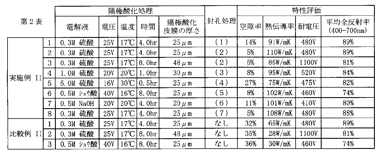
これに対し、封孔処理を施して、陽極酸化皮膜の空隙率が30%以下とした絶縁基板(実施例II-1~8)は、陽極酸化皮膜の厚くしても放熱性の低減を抑制することができ、絶縁性および放熱性のいずれにも優れることが分かった。
特に、陽極酸化皮膜の形成条件および膜厚が同じ値となる実施例II-1と比較例II-1とを対比すると、封孔処理を施して陽極酸化皮膜の空隙率を30%以下とすることにより、耐電圧と平均反射率を維持したまま、熱伝導率を向上できることが分かった。実施例II-3と比較例II-2との対比および実施例II-6と比較例II-3との対比からも同様のことが分かる。
実施例II-3で作製した絶縁基板(空隙率:5%)に対し、圧力を管理しながら酸素プラズマ処理を更に施し、実施例II-9の絶縁基板を作製した。
酸素プラズマ処理は、ヤマト科学社製のプラズマリアクターPR300を用い、80mL/分の酸素を流し、-0.1MPaになるように圧力を調整しながら、100Wの条件で4分間施した。
酸素プラズマ処理により、封孔処理によりマイクロポアの内部に封孔された水酸化アルミニウムの水酸基とイオン化した酸素とが反応して水として脱離され、表面層に存在していた水酸化アルミニウムは、酸化アルミニウムに変質し、体積収縮により除去された。
酸素プラズマ処理を施した後、絶縁基板表面をSEMで観察したところ、表面から2μm程度までの変質が観察され、次いで、AFMで5μm四方をタッピングモードで測定した結果、平均深さ1.8μmの凹部が平均ピッチ110nmの周期で存在していることが分かった。なお、実施例II-3で作製した絶縁基板表面をAFMで測定したところ、深さが0.3μmを超える凹部は観察されず、明確なピッチも検出できなかった。
また、上述した方法により酸素プラズマ処理後の陽極酸化皮膜の空隙率を算出したところ、空隙率は9%であった。
実施例II-3で作製した絶縁基板(空隙率:5%)に対し、更に1%NaOH溶液(液温:10℃)を用いてアルカリ処理を1分間施し、実施例II-10の絶縁基板を作製した。
アルカリ処理の後、10分間の水洗処理を施して乾燥させた後、絶縁基板表面をSEMで観察したところ、表面から約10μm程度までの変質が観察され、次いで、AFMで5μm四方をタッピングモードで測定した結果、平均深さ2μmの凹部が平均ピッチ100nmの周期で存在していることが分かった。
また、上述した方法によりアルカリ処理後の陽極酸化皮膜の空隙率を算出したところ、空隙率は12%であった。
(1)Niシード層の形成
まず、1000mLビーカーに硫酸ニッケル六水和物25gと純水500mLとを入れ、硫酸ニッケル六水和物を溶解させた後、次亜リン酸ナトリウム20g、酢酸ナトリウム10gおよびクエン酸ナトリウム10gを入れて撹拌した。
次いで、純水を加えて全量を1000mLとした後、硫酸でpHを5に調整し、撹拌しながら、浴温を83℃に保持した。
本溶液中に各絶縁基板を1分間浸漬させることで、Niシード層を形成した。
(2)Cuめっき層の形成
硫酸、硫酸銅、塩酸、ポリエチレングリコールおよびラウリル硫酸ナトリウムを調製した電解液中に、Niシード層を形成した上記基板を浸漬し、定電圧下で電解し、厚さ20μmのCuめっき層を形成した。
(3)金属配線の形成
Cuめっき層を形成した上記基板をレジスト液(DSR330P、タムラ化研社製)に25℃で浸漬時間5分の条件で浸漬させた後、乾燥温度80℃、乾燥時間10分にて乾燥させた。
次いで、FL-3S(ウシオライティング社製)を用いて、配線パターンを形成したマスクを用いて露光を行い、現像液1%炭酸ナトリウム水溶液を用いて30℃下で90秒間現像処理を施し、不要なレジスト層を除去した。
次いで、上記方法でパターンが形成された基板を過酸化水素溶液に浸漬し、エッチング処理を施すことで非配線部のCu層およびNiシード層を剥離した。
次いで、残りのレジスト層を除去し、Cu配線が形成された配線基板を作製した。
(4)Auめっき層の形成
Cu配線が形成された配線基板に対して、ワイアボンディング適性を付与するためにNiストライクめっきを行い、更にNiストライクめっき層の上層にAuめっき層を設けた。
Niストライクめっきは、Ni/塩酸混合液を用いて5分間処理した。
その後、プレシャスハブACG2000(田中貴金属社製)の基本液と還元液とを10:0.4の割合で調製した液中に、50℃の条件で10分間浸漬し、Auめっき層を形成した。
一方、実施例II-1~8で作製した絶縁基板を用いた場合、上記のような問題は発生しなかったが、形成したCu配線の細線部分との密着性がやや劣る結果が得られた。
また、実施例II-9および10で作製した絶縁基板を用いた場合、上記のような問題は発生せず、かつ、形成したCu配線の細線部分との密着性にも優れることが分かった。これは、実施例II-9および10で作製した絶縁基板の表面が有する凹凸形状により、Cu配線とのアンカー効果が生じているためと考えられる。
まず、比較例II-2で作製した絶縁基板(未封孔、空隙率:36%)に対して、撥水性材料(パーフルオロヘキシルエチルメトキシシラン[CF3(CF2)5CH2CH2Si(OCH3)3](Gelest社製))を精製せずにそのままインクジェット装置(DMT-2831、Dimatix社製)を用いて配線状に突出、付着させた後に乾燥させた。
その後、上述した封孔処理(1)と同様の封孔処理を施した。なお、上述した方法により陽極酸化皮膜の空隙率を算出したところ、空隙率は18%であった。
次いで、アルカリによる溶解処理(1%NaOH溶液、液温度:30℃、処理時間:20秒間)を施し、ほぼ単層のフッ素(フルオロアルキルシラン)皮膜を除去した。
この状態でNiを蒸着し、全面にNiシード層を形成した。
引き続き、上記(2)~(4)に示す工程と同様の方法で、Cu配線基板を作製した。
ここで、上記(3)に示す工程において、非配線部の封孔処理されていた部分はNiシード層の溶解が容易となり、かつ、上記(4)に示す工程で施されるNiストライクめっきおよびAuめっきにおいても非配線部への金属の析出は観察されなかった。
(実施例III-1~12、比較例III-1および2)
(1)アルミニウム基板の前処理工程(電解研磨処理)
高純度アルミニウム基板(住友軽金属社製、純度99.99質量%、厚み0.4mm)を、10cm四方の面積で陽極酸化処理できるようカットした後、以下組成の電解研磨液を用いて、電圧25V、液温度65℃、液流速3.0m/minの条件で電解研磨処理を施した。
陰極はカーボン電極とし、電源は、GP0110-30R(高砂製作所社製)を用いた。また、電解液の流速は渦式フローモニターFLM22-10PCW(AS ONE製)を用いて計測した。
なお、実施例III-8については、上記電解研磨処理を施さなかった。
・85質量%リン酸(和光純薬社製試薬) 660mL
・純水 160mL
・硫酸 150mL
・エチレングリコール 30mL
まず、電解研磨処理後のアルミニウム基板(実施例III-8については高純度アルミニウム基板)に、0.30mol/L硫酸の電解液で、電圧25V、液温度15℃、液流速3.0m/minの条件で1時間陽極酸化処理を施した。更に陽極酸化処理後のサンプルに、0.5mol/Lリン酸の混合水溶液を用いて40℃の条件で20分間浸漬して脱膜処理を施した。
次いで、これらと同様の処理をこの順に第3表記載の回数を繰り返した後、0.30mol/L硫酸の電解液で、電圧25V、液温度15℃、液流速3.0m/minの条件で、陽極酸化皮膜の厚み(TO)が第3表記載の厚さとなるよう陽極処理時間を設定して再陽極酸化処理を施し、更に、0.5mol/Lリン酸の混合水溶液を用いて40℃の条件で15分間浸漬させて脱膜処理を施すことにより、アルミニウム基板表面に、マイクロポアが直管状で且つハニカム状に配列された陽極酸化皮膜を形成させた。
なお、再陽極酸化処理の処理時間を決める基準とした陽極酸化皮膜の厚み(TO)は、再陽極酸化処理後に脱膜処理を施した後の最終的な陽極酸化皮膜の厚みのことをいう。
第1陽極酸化処理工程の後、濃度0.5mol/Lのホウ酸、濃度0.05mol/Lの四ホウ酸ナトリウムの混合水溶液にて、温度20℃で5分間処理し、マイクロポアが形成されていない部分の陽極酸化皮膜の厚み(TF)が第3表記載の厚さとなるよう電圧を設定して陽極酸化皮膜を形成し、絶縁基板を作製した。
なお、比較例III-2については、上記第2陽極酸化処理工程(陽極酸化処理)を施さなかった。
得られた絶縁基板について、絶縁基板の厚み(TA)、陽極酸化皮膜の厚み(TO)およびマイクロポアが形成されていない部分の上記陽極酸化皮膜の厚み(TF)を、それぞれ断面方向からのFE-SEMの観察により、10箇所の測定平均値から算出した。結果を第3表に示す。
得られた絶縁基板について、FE-SEMによる表面写真(倍率20000倍)の1μm×1μmの視野で任意のマイクロポア300個を用いて、上記式(i)で定義される規則化度を求めた。結果を第3表に示す。
得られた絶縁基板について、JISC2110規格の方法に従い、絶縁破壊電圧を計測した。結果を第3表に示す。
絶縁破壊電圧が150以上あれば、絶縁性に優れ、白色系の発光出力を向上させることができると評価できる。
得られた絶縁基板について、アルバック理工社製TC-9000/レーザーフラッシュ型熱拡散率測定装置を用い、t1/2法に従い熱伝導率を計測した。結果を第3表に示す。
熱伝導率が200程度以上あれば、放熱性に優れ、白色系の発光出力を向上させることができると評価できる。
得られた絶縁基板について、エックスライト社製SP64を用いて400~700nmの全反射率を計測した。結果を第3表に示す。
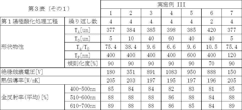
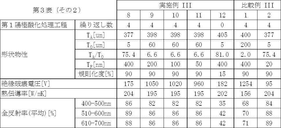
また、陽極酸化皮膜の深さ方向の厚みのうち上記マイクロポアが形成されていない部分の厚み(TF)が小さい比較例III-2で作製した絶縁基板は、絶縁破壊電圧が低く、絶縁性に劣ることが分かった。
一方、上記厚み(TA)、上記厚み(TO)およびこれらの比率(TA/TO)ならびに上記厚み(TF)の値がすべて所定範囲にある実施例III-1~12で作製した絶縁基板は、絶縁性および放熱性に優れ、白色系の発光出力を向上させた発光素子を提供できることが分かった。特に、マイクロポアの規則化度の高い実施例III-1~11で作製した絶縁基板は、全反射率も高く、発光素子の輝度を向上できることが分かった。また、上記陽極酸化皮膜の厚み(TO)が20~70μmの範囲にあり、かつ、上記陽極酸化皮膜の厚み(TO)に対する上記絶縁基板の厚み(TA)の比率(TA/TO)が8~12の範囲にある実施例III-3~6および9~11で作製した絶縁基材は、絶縁性が極めて高くなることが分かった。
2 アルミニウム基板
3 陽極酸化皮膜
4 スルーホール
5 銅配線
6 電極
7 導体金属
7a 残部
7b 不要部
8 金属箔層
9 チップ
10 連結部
11 切欠部
12 切離跡
13 配線パターン
14 陽極酸化皮膜
15、15a、15b マイクロポア
16 異なる物質
17 絶縁基板
18 アルミニウム基板
19 絶縁層
20 マイクロポア
22 青色LED
24 樹脂
26 蛍光発光ユニット
32 絶縁層
33 金属基板
34 金属配線層
35 スルーホール
37 青色LED
39 ヒートシンク
100 発光素子
101、102、104、105、107、108 マイクロポア
103、106、109 円
110 青色LED
120,130 金属配線層(電極)
140 配線基板
150 蛍光粒子
160 透明樹脂
200 発光素子
222 青色LED発光素子
224 樹脂
226 蛍光発光体
230 絶縁基板
232 絶縁層
233 アルミニウム基板
300 発光素子
310 青色LED
320,330 電極
340 基板
350 蛍光粒子
360 透明樹脂
410 陽極酸化処理装置
412 給電槽
414 電解処理槽
416 アルミニウム基板
418、426 電解液
420 給電電極
422、428 ローラ
424 ニップローラ
430 電解電極
432 槽壁
434 直流電源
Claims (35)
- アルミニウム基板と、
前記アルミニウム基板の全面を被覆する陽極酸化皮膜と、を備え、
前記陽極酸化皮膜中において、円相当直径1μm以上の金属間化合物が2000個/mm3以下である絶縁基板。 - さらに、前記アルミニウム基板の厚さ方向に貫通形成されたスルーホールを備え、
前記スルーホールの内壁面が前記陽極酸化皮膜で被覆されている、請求項1に記載の絶縁基板。 - 前記アルミニウム基板のアルミニウム純度が99.95質量%以上である、請求項1または2に記載の絶縁基板。
- LED用絶縁基板である、請求項1~3のいずれかに記載の絶縁基板。
- 請求項1に記載の絶縁基板を得る絶縁基板の製造方法であって、
アルミニウム基板に対して陽極酸化処理を施す陽極酸化処理工程を備え、前記アルミニウム基板の全面を被覆する陽極酸化皮膜中において円相当直径1μm以上の金属間化合物が2000個/mm3以下である絶縁基板を得る絶縁基板の製造方法。 - 請求項2に記載の絶縁基板を得る絶縁基板の製造方法であって、
前記陽極酸化処理工程の前に、前記アルミニウム基板の厚さ方向にスルーホールを貫通形成するスルーホール形成工程を備える、請求項5に記載の絶縁基板の製造方法。 - 前記陽極酸化処理工程の前に、前記アルミニウム基板に対して350~600℃での焼鈍処理を施す焼鈍処理工程を備える、請求項5または6に記載の絶縁基板の製造方法。
- 前記陽極酸化処理工程では、硫酸電解液を用いる、請求項5~7のいずれかに記載の絶縁基板の製造方法。
- 前記硫酸電解液の硫酸濃度が、10~60g/lである、請求項8に記載の絶縁基板の製造方法。
- 前記アルミニウム基板のアルミニウム純度が99.95質量%以上である、請求項5~9のいずれかに記載の絶縁基板の製造方法。
- 請求項1~3のいずれかに記載の絶縁基板が備える前記陽極酸化皮膜上の所望部位に配線を形成する配線の形成方法であって、前記所望部位にのみ前記配線となる導体金属を選択的に供給する供給工程を備える、配線の形成方法。
- 前記供給工程が、前記所望部位に前記導体金属を含む金属インクをインクジェット印刷法により供給する工程である、請求項11に記載の配線の形成方法。
- 前記供給工程が、前記所望部位に前記導体金属を含む金属インクをスクリーン印刷法により供給する工程である、請求項11に記載の配線の形成方法。
- 前記供給工程が、前記陽極酸化皮膜上の前記所望部位以外の部位にレジストを形成させた前記絶縁基板に対して、前記導体金属のイオンを含有する処理液を用いて無電解めっき処理および/または電解めっき処理を施す工程である、請求項11に記載の配線の形成方法。
- 前記供給工程が、前記所望部位に金属還元能を有する金属還元層を形成し、形成された前記金属還元層に対して前記導体金属のイオンを含有する処理液を接触させる工程である、請求項11に記載の配線の形成方法。
- 前記所望部位が前記絶縁基板の表裏両側に位置している、請求項11~15のいずれかに記載の配線の形成方法。
- 金属基板と、前記金属基板の表面に設けられる絶縁層とを有する絶縁基板であって、
前記金属基板が、バルブ金属基板であり、
前記絶縁層が、バルブ金属の陽極酸化皮膜であり、
前記陽極酸化皮膜の空隙率が、30%以下である絶縁基板。 - 前記陽極酸化皮膜の表面が、平均ピッチが0.5μm以下で、かつ、平均直径が1μm以上の凹凸を有する請求項17に記載の絶縁基板。
- 前記陽極酸化皮膜が、マイクロポアを有し、
前記マイクロポアの内部の少なくとも一部が、前記陽極酸化皮膜を構成する物質とは異なる物質によって封孔されている請求項17または18に記載の絶縁基板。 - 前記陽極酸化皮膜が、マイクロポアを有し、
前記マイクロポアが、その内部の少なくとも一部が前記陽極酸化皮膜を構成する物質とは異なる物質によって封孔されているマイクロポアと、その内部が前記異なる物質により封孔されていないマイクロポアとで構成されている請求項17~19のいずれかに記載の絶縁基板。 - 前記異なる物質が、絶縁性である請求項19または20に記載の絶縁基板。
- 前記バルブ金属が、アルミニウム、タンタル、ニオブ、チタン、ハフニウム、ジルコニウム、亜鉛、タングステン、ビスマスおよびアンチモンからなる群から選択される少なくとも1種の金属である請求項17~21のいずれかに記載の絶縁基板。
- 前記バルブ金属が、アルミニウムである請求項22に記載の絶縁基板。
- 前記絶縁基板が、LED発光素子の発光観測面側に設けられる基板である請求項17~23のいずれかに記載の絶縁基板。
- 請求項17~24のいずれかに記載の絶縁基板を製造する絶縁基板の製造方法であって、
バルブ金属基板の表面に陽極酸化処理を施して、バルブ金属の陽極酸化皮膜をバルブ金属基板上に形成させる陽極酸化処理工程と、
前記陽極酸化処理工程の後に、封孔処理を施して、前記陽極酸化皮膜の空隙率を30%以下とする封孔処理工程とを有する絶縁基板の製造方法。 - 前記陽極酸化処理により、マイクロポアを有する前記陽極酸化皮膜が形成され、
前記封孔処理により、前記マイクロポアの内部の少なくとも一部が前記陽極酸化皮膜を構成する物質とは異なる物質により封孔される、請求項25に記載の絶縁基板の製造方法。 - 前記バルブ金属基板の厚さ方向にスルーホールを貫通形成するスルーホール形成工程を有する、請求項25または26に記載の絶縁基板の製造方法。
- 前記スルーホール形成工程の後に、前記バルブ金属基板を所望の形状で個片化可能にする個片化工程を有する請求項27に記載の絶縁基板の製造方法。
- 請求項17~24のいずれかに記載の絶縁基板と、前記絶縁基板の前記絶縁層側の上部に設けられる金属配線層とを有する配線基板。
- 請求項29に記載の配線基板と、前記配線基板の前記金属配線層側の上部に設けられる青色LED発光素子と、前記青色LED発光素子の少なくとも上部に設けられる蛍光発光体とを具備する白色系LED発光素子。
- アルミニウム基板と、前記アルミニウム基板の表面に設けられる絶縁層とを有する絶縁基板であって、
前記絶縁層が、マイクロポアを有する、アルミニウムの陽極酸化皮膜であり、
前記絶縁基板の厚みが1500μm以下であり、
前記陽極酸化皮膜の厚みが5μm以上であり、
前記陽極酸化皮膜の厚み(TO)に対する前記絶縁基板の厚み(TA)の比率(TA/TO)が2.5~300であり、
前記陽極酸化皮膜の深さ方向の厚みのうち、前記マイクロポアが形成されていない部分の厚みが30nm以上である絶縁基板。 - 前記マイクロポアについて下記式(i)により定義される規則化度が20%以上である、請求項31に記載の絶縁基板。
規則化度(%)=B/A×100 (i)
前記式(i)中、Aは、測定範囲におけるマイクロポアの全数を表す。Bは、一のマイクロポアの重心を中心とし、他のマイクロポアの縁に内接する最も半径が短い円を描いた場合に、その円の内部に前記一のマイクロポア以外のマイクロポアの重心を6個含むことになる前記一のマイクロポアの測定範囲における数を表す。 - 前記絶縁基板が、LED発光素子の発光観測面側に設けられる基板である請求項31または32に記載の絶縁基板。
- 請求項31~33のいずれかに記載の絶縁基板を製造する絶縁基板の製造方法であって、
アルミニウム基板の一部に陽極酸化処理を施して、マイクロポアを有する、アルミニウムの陽極酸化皮膜をアルミニウム基板上に形成させる第1陽極酸化処理工程と、
前記第1陽極酸化処理工程の後に、pH2.5~11.5の電解液を用いて陽極酸化処理を施して、前記マイクロポアの内部の一部を底方向から酸化アルミニウムで封孔する第2陽極酸化処理工程とを有する絶縁基板の製造方法。 - 請求項31~33のいずれかに記載の絶縁基板と、前記絶縁基板の前記絶縁層側の上部に設けられる青色LED発光素子と、前記青色LED発光素子の少なくとも上部に設けられる蛍光発光体とを具備する白色系LED発光素子。
Priority Applications (3)
| Application Number | Priority Date | Filing Date | Title |
|---|---|---|---|
| US13/518,770 US20120256224A1 (en) | 2009-12-25 | 2010-12-14 | Insulated substrate, process for production of insulated substrate, process for formation of wiring line, wiring substrate, and light-emitting element |
| CN2010800592112A CN102666940A (zh) | 2009-12-25 | 2010-12-14 | 绝缘基板、绝缘基板制备方法、配线形成方法、配线基板、和发光器件 |
| EP10839243A EP2518190A1 (en) | 2009-12-25 | 2010-12-14 | Insulated substrate, process for production of insulated substrate, process for formation of wiring line, wiring substrate, and light-emitting element |
Applications Claiming Priority (10)
| Application Number | Priority Date | Filing Date | Title |
|---|---|---|---|
| JP2009295050A JP2011132586A (ja) | 2009-12-25 | 2009-12-25 | 絶縁基板および発光素子 |
| JP2009-295050 | 2009-12-25 | ||
| JP2010-009826 | 2010-01-20 | ||
| JP2010009826 | 2010-01-20 | ||
| JP2010-042287 | 2010-02-26 | ||
| JP2010042287 | 2010-02-26 | ||
| JP2010-064186 | 2010-03-19 | ||
| JP2010064186A JP2011171687A (ja) | 2010-01-20 | 2010-03-19 | 絶縁基板、その製造方法および配線の形成方法 |
| JP2010-097856 | 2010-04-21 | ||
| JP2010097856A JP2011199233A (ja) | 2010-02-26 | 2010-04-21 | 絶縁基板およびその製造方法 |
Publications (1)
| Publication Number | Publication Date |
|---|---|
| WO2011078010A1 true WO2011078010A1 (ja) | 2011-06-30 |
Family
ID=46774767
Family Applications (1)
| Application Number | Title | Priority Date | Filing Date |
|---|---|---|---|
| PCT/JP2010/072463 Ceased WO2011078010A1 (ja) | 2009-12-25 | 2010-12-14 | 絶縁基板、絶縁基板の製造方法、配線の形成方法、配線基板および発光素子 |
Country Status (5)
| Country | Link |
|---|---|
| US (1) | US20120256224A1 (ja) |
| EP (1) | EP2518190A1 (ja) |
| KR (1) | KR20120109573A (ja) |
| CN (1) | CN102666940A (ja) |
| WO (1) | WO2011078010A1 (ja) |
Cited By (7)
| Publication number | Priority date | Publication date | Assignee | Title |
|---|---|---|---|---|
| US20130337273A1 (en) * | 2012-06-13 | 2013-12-19 | International Business Machines Corporation | Thermal interface material (tim) with thermally conductive integrated release layer |
| CN103668381A (zh) * | 2012-09-04 | 2014-03-26 | 中国科学院宁波材料技术与工程研究所 | 一种绝缘基片上原位多孔氧化铝膜的制备方法 |
| US9186641B2 (en) | 2011-08-05 | 2015-11-17 | International Business Machines Corporation | Microcapsules adapted to rupture in a magnetic field to enable easy removal of one substrate from another for enhanced reworkability |
| US9283514B2 (en) | 2011-01-21 | 2016-03-15 | International Business Machines Corporation | Silicone-based chemical filter and silicone-based chemical bath for removing sulfur contaminants |
| US9303047B2 (en) | 2011-05-06 | 2016-04-05 | International Business Machines Corporation | Flame retardant filler |
| US9307692B2 (en) | 2011-10-28 | 2016-04-12 | International Business Machines Corporation | Microcapsules adapted to rupture in a magnetic field |
| JP2019147988A (ja) * | 2018-02-27 | 2019-09-05 | 富士フイルム株式会社 | 金属膜、構造体、複合材料、金属膜の製造方法、構造体の製造方法、および複合材料の製造方法 |
Families Citing this family (31)
| Publication number | Priority date | Publication date | Assignee | Title |
|---|---|---|---|---|
| CN203260631U (zh) * | 2010-07-01 | 2013-10-30 | 西铁城控股株式会社 | Led光源装置 |
| WO2013180119A1 (ja) * | 2012-05-30 | 2013-12-05 | 三菱レイヨン株式会社 | モールドの製造方法および微細凹凸構造を表面に有する成形体の製造方法 |
| JP5937937B2 (ja) * | 2012-09-26 | 2016-06-22 | 株式会社神戸製鋼所 | アルミニウム陽極酸化皮膜 |
| US9484621B2 (en) * | 2012-11-02 | 2016-11-01 | Nokia Technologies Oy | Portable electronic device body having laser perforation apertures and associated fabrication method |
| US20140209961A1 (en) * | 2013-01-30 | 2014-07-31 | Luxo-Led Co., Limited | Alternating current light emitting diode flip-chip |
| CN105518883B (zh) * | 2013-09-05 | 2018-09-14 | 夏普株式会社 | 发光装置用基板、发光装置、以及发光装置用基板的制造方法 |
| CN103742874A (zh) * | 2013-12-31 | 2014-04-23 | 河南云华灿光电科技有限公司 | 铝基板机构以及具有该铝基板机构的led球泡灯 |
| WO2015115531A1 (ja) * | 2014-01-31 | 2015-08-06 | 富士フイルム株式会社 | アルミニウム板の製造方法、アルミニウム板、蓄電デバイス用集電体および蓄電デバイス |
| US10351958B2 (en) * | 2014-06-20 | 2019-07-16 | Council On Postsecondary Education | Systems and methods for electroless plating of thin gold films directly onto silicon nitride and into pores in silicon nitride |
| KR101630769B1 (ko) * | 2014-06-24 | 2016-06-16 | 매그나칩 반도체 유한회사 | 방열 반도체 칩 패키지 및 그 제조 방법 |
| CN104157580B (zh) * | 2014-08-12 | 2017-06-06 | 上海航天电子通讯设备研究所 | 基于铝阳极氧化技术的埋置芯片互连封装方法及结构 |
| JP6328785B2 (ja) * | 2014-10-14 | 2018-05-23 | 富士フイルム株式会社 | アルミニウム板およびアルミニウム板の製造方法 |
| CN104451818A (zh) * | 2014-11-17 | 2015-03-25 | 中国人民解放军空军工程大学 | 一种绝缘金属板及其制作方法 |
| US10479894B2 (en) * | 2014-12-03 | 2019-11-19 | Sk Innovation Co., Ltd. | Solution for fabricating nano particles |
| US10269428B2 (en) | 2014-12-03 | 2019-04-23 | Sk Innovation Co., Ltd. | Nano structures, device using the same, and method for fabricating the nano structures |
| US20160159988A1 (en) * | 2014-12-03 | 2016-06-09 | Sk Innovation Co., Ltd. | Polymer solution for fabricating nano particles |
| DE102015108420A1 (de) * | 2015-05-28 | 2016-12-01 | Osram Opto Semiconductors Gmbh | Verfahren zur Herstellung eines Trägerelements, Trägerelement und elektronisches Bauelement mit einem Trägerelement |
| JP6450296B2 (ja) * | 2015-10-05 | 2019-01-09 | 浜松ホトニクス株式会社 | 配線構造体、及び配線構造体の製造方法 |
| CN105463549B (zh) * | 2015-12-03 | 2018-06-26 | 中国航空工业集团公司北京航空材料研究院 | 一种提高铝及铝合金防护性能的阳极化方法 |
| JP6759784B2 (ja) * | 2016-07-12 | 2020-09-23 | 三菱電機株式会社 | 半導体モジュール |
| JP6758387B2 (ja) * | 2016-09-02 | 2020-09-23 | 富士フイルム株式会社 | 蛍光体含有フィルムおよびバックライトユニット |
| AR106253A1 (es) * | 2016-10-04 | 2017-12-27 | Di Ciommo José Antonio | Cable aéreo para transporte de energía eléctrica en baja y media tensión y de señales digitales, de conductores concéntricos de aleación de aluminio conteniendo dentro un cable de fibra óptica y proceso de tratamiento de alambre trefilado |
| US10675797B2 (en) * | 2017-02-07 | 2020-06-09 | Dong Guan Qinde Metal Products Co., Ltd. | Stainless steel and synthetic resin composite molded body, and preparation method thereof |
| JP6515940B2 (ja) * | 2017-03-17 | 2019-05-22 | 日亜化学工業株式会社 | 発光装置及びその製造方法 |
| US10180247B1 (en) * | 2017-07-03 | 2019-01-15 | Valeo North America, Inc. | Device and method for placement of light source on a heat sink |
| US11312107B2 (en) * | 2018-09-27 | 2022-04-26 | Apple Inc. | Plugging anodic oxides for increased corrosion resistance |
| CN109112521A (zh) * | 2018-10-29 | 2019-01-01 | 重庆立道新材料科技有限公司 | 一种无铬钝化剂及其制备方法 |
| CN112712764B (zh) * | 2019-10-24 | 2022-09-02 | 深圳市百柔新材料技术有限公司 | 显示面板的制造方法 |
| CN114599167B (zh) * | 2021-08-23 | 2023-08-01 | 常州海弘电子有限公司 | 一种厚铜pcb板焊接面防耐擦花处理工艺 |
| KR102708646B1 (ko) * | 2022-03-11 | 2024-09-24 | (주)포인트엔지니어링 | 양극산화막 구조체 및 이를 포함하는 검사 장치 |
| KR20240050065A (ko) * | 2022-10-11 | 2024-04-18 | (주)포인트엔지니어링 | 가이드 플레이트 및 이를 포함하는 검사 장치 |
Citations (159)
| Publication number | Priority date | Publication date | Assignee | Title |
|---|---|---|---|---|
| US2708655A (en) | 1955-05-17 | Electrolytic polishing of aluminum | ||
| GB1222777A (en) | 1968-09-27 | 1971-02-17 | Leichtmetall Werke Gmbh Van | Printing plates for rotary offset printing machines |
| JPS4826638A (ja) | 1971-08-11 | 1973-04-07 | ||
| JPS4845303A (ja) | 1971-10-07 | 1973-06-28 | ||
| GB1421710A (en) | 1974-08-27 | 1976-01-21 | British Aluminium Co Ltd | Lithographic printing plate alloy |
| JPS5412853A (en) | 1977-06-30 | 1979-01-30 | Ricoh Co Ltd | Laser beam modulating system |
| JPS5481133A (en) | 1977-12-12 | 1979-06-28 | Fuji Photo Film Co Ltd | Anodic oxidation device |
| JPS5442284B2 (ja) | 1974-11-25 | 1979-12-13 | ||
| JPS5528874B2 (ja) | 1976-07-20 | 1980-07-30 | ||
| JPS55154564U (ja) | 1979-04-24 | 1980-11-07 | ||
| JPS5612518B2 (ja) | 1974-09-12 | 1981-03-23 | ||
| JPS5747894A (en) | 1980-09-05 | 1982-03-18 | Fuji Photo Film Co Ltd | Electrolytic treatment of strip-like metallic sheet |
| JPS5751289A (en) | 1980-09-10 | 1982-03-26 | Fuji Photo Film Co Ltd | Electrolytic treating device for belt-like metallic plate |
| JPS5751290A (en) | 1980-09-10 | 1982-03-26 | Fuji Photo Film Co Ltd | Electrolytic treatment of beltlike metallic plate |
| JPS5754300A (ja) | 1980-09-19 | 1982-03-31 | Fuji Photo Film Co Ltd | Obijokinzokubannodenkaisochi |
| JPS57136596A (en) | 1981-02-19 | 1982-08-23 | Toyama Chem Co Ltd | Carcinostatic substance tf-240, its preparation, and carcinostatic agent containing the same |
| JPS5811759A (ja) | 1981-07-14 | 1983-01-22 | Furukawa Alum Co Ltd | 印刷用アルミニウム素板 |
| JPS5842493A (ja) | 1981-09-07 | 1983-03-11 | Furukawa Alum Co Ltd | オフセツト印刷用アルミニウム合金板の製造方法 |
| JPS5824517B2 (ja) | 1980-04-02 | 1983-05-21 | 勝川工業株式会社 | 直流電解による連続コイルアルマイトの片面専用処理装置 |
| JPS58107498A (ja) | 1981-12-18 | 1983-06-27 | Fuji Photo Film Co Ltd | 帯状金属板の電解処理方法および装置 |
| JPS58221254A (ja) | 1982-06-18 | 1983-12-22 | Furukawa Alum Co Ltd | オフセツト印刷用アルミニウム素板 |
| JPS59107592A (ja) * | 1982-12-13 | 1984-06-21 | ティーディーケイ株式会社 | プリント配線用基板 |
| JPS59153861A (ja) | 1983-02-22 | 1984-09-01 | Fuji Photo Film Co Ltd | 平版印刷版用支持体 |
| JPS6063347A (ja) | 1983-09-16 | 1985-04-11 | Kobe Steel Ltd | 印刷版用高強度アルミニウム合金冷間圧延板 |
| JPS6063346A (ja) | 1983-09-16 | 1985-04-11 | Kobe Steel Ltd | 印刷版用高強度アルミニウム合金冷間圧延板 |
| JPS60200256A (ja) | 1984-03-23 | 1985-10-09 | Fuji Photo Film Co Ltd | 感光性平版印刷版の処理方法 |
| JPS60203497A (ja) | 1984-03-28 | 1985-10-15 | Fuji Photo Film Co Ltd | 平版印刷版用アルミニウム基材及び平版印刷版用アルミニウム支持体の製造方法 |
| JPS60203496A (ja) | 1984-03-28 | 1985-10-15 | Fuji Photo Film Co Ltd | 平版印刷版用アルミニウム基材及び平版印刷版用アルミニウム支持体の製造法 |
| JPS60215725A (ja) | 1984-04-06 | 1985-10-29 | Sukai Alum Kk | 印刷用アルミニウム合金素板 |
| JPS60215727A (ja) | 1984-04-06 | 1985-10-29 | Sukai Alum Kk | 印刷用アルミニウム合金素板 |
| JPS60215726A (ja) | 1984-04-06 | 1985-10-29 | Sukai Alum Kk | 印刷用アルミニウム合金素板 |
| JPS60216728A (ja) | 1984-04-09 | 1985-10-30 | 長野日本無線株式会社 | 無停電電源装置 |
| JPS60230951A (ja) | 1984-04-27 | 1985-11-16 | Fuji Photo Film Co Ltd | 平版印刷版用アルミニウム合金支持体 |
| JPS6135995A (ja) | 1984-07-13 | 1986-02-20 | ヘキスト・アクチエンゲゼルシヤフト | 印刷板用支持体および印刷板 |
| JPS6151395A (ja) | 1984-08-21 | 1986-03-13 | Fuji Photo Film Co Ltd | 平版印刷版用支持体の製造方法 |
| JPS61201747A (ja) | 1985-03-02 | 1986-09-06 | フエルアイニヒテ・アルミニウム‐ウエルケ・アクチエンゲゼルシヤフト | アルミニウム製オフセツト用ベルトおよびその製造方法 |
| JPS61272367A (ja) | 1985-05-28 | 1986-12-02 | Mitsubishi Electric Corp | 薄膜形成装置 |
| JPS61274993A (ja) | 1985-05-31 | 1986-12-05 | Nippon Light Metal Co Ltd | オフセツト印刷用アルミニウム合金支持体 |
| JPS6223794A (ja) | 1985-07-25 | 1987-01-31 | Nippon Light Metal Co Ltd | オフセツト印刷用アルミニウム合金支持体 |
| JPS625080B2 (ja) | 1981-09-03 | 1987-02-03 | Furukawa Aruminiumu Kogyo Kk | |
| JPS6286143A (ja) | 1985-10-11 | 1987-04-20 | Sky Alum Co Ltd | 印刷版支持体用アルミニウム合金素板 |
| JPS62136596A (ja) | 1985-12-09 | 1987-06-19 | Fuji Photo Film Co Ltd | 金属ウエブへの連続電解処理装置 |
| JPS62140894A (ja) | 1985-12-16 | 1987-06-24 | Sky Alum Co Ltd | 平版印刷版用アルミニウム合金支持体 |
| JPS62146694A (ja) | 1985-12-23 | 1987-06-30 | Nippon Light Metal Co Ltd | 平版印刷用アルミニウム合金支持体の製造法 |
| JPS62148295A (ja) | 1985-12-23 | 1987-07-02 | Furukawa Alum Co Ltd | 平版印刷版用アルミニウム合金支持体およびその製造方法 |
| JPS62149856A (ja) | 1985-12-23 | 1987-07-03 | Sky Alum Co Ltd | 平版印刷版用アルミニウム合金支持体の製造方法 |
| JPS62181191A (ja) | 1986-02-06 | 1987-08-08 | Furukawa Alum Co Ltd | 平版印刷原版の製造方法 |
| JPS6330294A (ja) | 1986-07-24 | 1988-02-08 | Fuji Photo Film Co Ltd | 平版印刷版用アルミニウム合金支持体およびその製造方法 |
| JPS6347349A (ja) | 1986-08-18 | 1988-02-29 | Sky Alum Co Ltd | 平版印刷版用アルミニウム合金支持体 |
| JPS6347347A (ja) | 1986-08-18 | 1988-02-29 | Sky Alum Co Ltd | 平版印刷版用アルミニウム合金支持体 |
| JPS6347348A (ja) | 1986-08-18 | 1988-02-29 | Sky Alum Co Ltd | 平版印刷版用アルミニウム合金支持体 |
| JPS6387288A (ja) | 1986-09-30 | 1988-04-18 | Fuji Photo Film Co Ltd | 平版印刷版用支持体の製造方法 |
| JPS63135294A (ja) | 1986-11-27 | 1988-06-07 | Furukawa Alum Co Ltd | 平版印刷版用アルミニウム合金支持体およびその製造方法 |
| JPS63143234A (ja) | 1986-12-06 | 1988-06-15 | Mitsubishi Alum Co Ltd | 印刷版用アルミニウム合金 |
| JPS63143235A (ja) | 1986-12-06 | 1988-06-15 | Mitsubishi Alum Co Ltd | 印刷版用アルミニウム合金 |
| JPS63176494A (ja) | 1987-01-16 | 1988-07-20 | Fuji Photo Film Co Ltd | 電解処理用通電ロ−ル |
| JPS6360824B2 (ja) | 1983-01-20 | 1988-11-25 | ||
| JPS6360823B2 (ja) | 1983-01-20 | 1988-11-25 | ||
| JPS641293A (en) | 1987-06-24 | 1989-01-05 | Hitachi Ltd | Aligner |
| JPS6451992A (en) | 1987-04-28 | 1989-02-28 | Vaw Ver Aluminium Werke Ag | Foundation material for offset printing block made of aluminum and manufacture thereof |
| US4818300A (en) | 1986-12-08 | 1989-04-04 | Aluminum Company Of America | Method for making lithoplate |
| JPH0135910B2 (ja) | 1982-10-12 | 1989-07-27 | Kobe Seikosho Kk | |
| JPH01293350A (ja) | 1988-05-23 | 1989-11-27 | Canon Inc | 電子写真感光体 |
| JPH01306288A (ja) | 1988-06-06 | 1989-12-11 | Fuji Photo Film Co Ltd | 平版印刷版用支持体 |
| EP0223737B1 (de) | 1985-10-30 | 1989-12-27 | Schweizerische Aluminium Ag | Träger für eine lithographische Druckplatte |
| JPH02215599A (ja) | 1989-02-17 | 1990-08-28 | Mitsubishi Alum Co Ltd | 平版印刷版用支持体 |
| JPH02293189A (ja) | 1989-05-09 | 1990-12-04 | Sumitomo Light Metal Ind Ltd | 平版印刷版用アルミニウム合金材料およびそれを用いた支持体の製造方法 |
| JPH0311635B2 (ja) | 1984-12-20 | 1991-02-18 | Furukawa Aruminiumu Kogyo Kk | |
| JPH0379798A (ja) | 1989-08-22 | 1991-04-04 | Fuji Photo Film Co Ltd | 平版印刷版用支持体の製造方法 |
| US5028276A (en) | 1990-02-16 | 1991-07-02 | Aluminum Company Of America | Method for making lithoplate having improved grainability |
| JPH03162530A (ja) | 1989-11-22 | 1991-07-12 | Nippon Light Metal Co Ltd | 金属溶湯の濾過方法 |
| JPH0361753B2 (ja) | 1983-06-22 | 1991-09-20 | Furukawa Aruminiumu Kogyo Kk | |
| JPH03222796A (ja) | 1990-01-30 | 1991-10-01 | Nippon Light Metal Co Ltd | 平版印刷版用アルミニウム支持体 |
| JPH03234594A (ja) | 1990-02-09 | 1991-10-18 | Sky Alum Co Ltd | 印刷版用アルミニウム合金支持体 |
| JPH0368939B2 (ja) | 1984-04-06 | 1991-10-30 | Sukai Aruminiumu Kk | |
| JPH044194A (ja) | 1990-04-20 | 1992-01-08 | Fuji Photo Film Co Ltd | 印刷版用支持体の表面処理装置 |
| JPH0419291B2 (ja) | 1983-09-16 | 1992-03-30 | Kobe Seikosho Kk | |
| JPH0419290B2 (ja) | 1983-09-16 | 1992-03-30 | Kobe Seikosho Kk | |
| JPH0419292B2 (ja) | 1983-09-16 | 1992-03-30 | Kobe Seikosho Kk | |
| JPH04165041A (ja) | 1990-10-26 | 1992-06-10 | Sky Alum Co Ltd | 印刷版支持体用アルミニウム合金素板およびその製造方法 |
| JPH04176897A (ja) | 1990-11-08 | 1992-06-24 | Riken Corp | 鋼製組合せオイルコントロールリングのレールリングのめっき処理方法 |
| JPH04231425A (ja) | 1990-12-27 | 1992-08-20 | Mitsui Mining & Smelting Co Ltd | 溶融アルミニウム濾過用セラミックスフィルター |
| JPH04254545A (ja) | 1991-02-01 | 1992-09-09 | Furukawa Alum Co Ltd | 平版印刷版用アルミニウム合金支持体 |
| JPH04276031A (ja) | 1991-03-05 | 1992-10-01 | Nippon Light Metal Co Ltd | アルミニウム中のリンの除去方法 |
| JPH04280997A (ja) | 1991-03-07 | 1992-10-06 | Fuji Photo Film Co Ltd | アルミニウム製品の連続電解処理装置 |
| JPH0473394B2 (ja) | 1986-02-06 | 1992-11-20 | Furukawa Aruminiumu Kogyo Kk | |
| JPH0473392B2 (ja) | 1985-09-30 | 1992-11-20 | Nippon Keikinzoku Kk | |
| JPH0524377A (ja) | 1991-07-26 | 1993-02-02 | Fuji Photo Film Co Ltd | 平版印刷版用支持体の陽極酸化方法 |
| JPH0532083A (ja) | 1991-07-29 | 1993-02-09 | Fuji Photo Film Co Ltd | 平版印刷版用支持体の陽極酸化方法 |
| JPH0551659A (ja) | 1991-08-21 | 1993-03-02 | Showa Alum Corp | アルミニウム溶湯中からの脱水素方法 |
| JPH05125597A (ja) | 1991-11-06 | 1993-05-21 | Fuji Photo Film Co Ltd | 平版印刷版用支持体の陽極酸化装置及び陽極酸化方法 |
| JPH05140659A (ja) | 1991-11-18 | 1993-06-08 | Mitsui Mining & Smelting Co Ltd | 傾斜出湯式濾過漕 |
| JPH05156414A (ja) | 1991-12-02 | 1993-06-22 | Fuji Photo Film Co Ltd | 平版印刷版用支持体の製造方法 |
| JPH0549148U (ja) | 1991-12-16 | 1993-06-29 | 日本重化学工業株式会社 | 金属溶湯脱ガス装置のガス噴射器 |
| JPH05179482A (ja) | 1991-11-05 | 1993-07-20 | Fuji Photo Film Co Ltd | 平版印刷版用支持体の封孔処理方法及び装置 |
| JPH05195291A (ja) | 1992-01-23 | 1993-08-03 | Fuji Photo Film Co Ltd | 陽極酸化処理方法及び装置 |
| JPH05201166A (ja) | 1992-01-23 | 1993-08-10 | Fuji Photo Film Co Ltd | 平版印刷版用支持体の製造方法 |
| JPH05202496A (ja) | 1992-01-27 | 1993-08-10 | Fuji Photo Film Co Ltd | 平版印刷版用支持体の封孔処理方法及び装置 |
| JPH0576530B2 (ja) | 1986-04-01 | 1993-10-22 | Furukawa Aluminium | |
| JPH05301478A (ja) | 1992-04-27 | 1993-11-16 | Fuji Photo Film Co Ltd | 平版印刷版支持体及びその製造方法 |
| JPH05304346A (ja) * | 1991-03-28 | 1993-11-16 | Sky Alum Co Ltd | アルミニウムベース回路基板 |
| JPH05311261A (ja) | 1992-05-13 | 1993-11-22 | Mitsui Mining & Smelting Co Ltd | 金属溶湯用濾過材 |
| JPH0626308A (ja) | 1992-07-09 | 1994-02-01 | Toshiba Corp | コンバインドサイクル発電プラント |
| JPH0635174A (ja) | 1992-07-16 | 1994-02-10 | Fuji Photo Film Co Ltd | 感光性平版印刷版およびその処理方法 |
| JPH0645515A (ja) | 1992-07-27 | 1994-02-18 | Sanyo Electric Co Ltd | 混成集積回路装置 |
| JPH0648058A (ja) | 1992-07-31 | 1994-02-22 | Fuji Photo Film Co Ltd | 平版印刷版用支持体の製造方法 |
| JPH0657432A (ja) | 1992-08-10 | 1994-03-01 | Matsushita Electric Ind Co Ltd | 酸化タンタル薄膜の形成方法 |
| JPH06122949A (ja) | 1992-10-08 | 1994-05-06 | Fuji Photo Film Co Ltd | 平版印刷版用支持体の製造方法 |
| JPH06136466A (ja) | 1992-10-26 | 1994-05-17 | Daido Steel Co Ltd | アルミニウム溶湯又はアルミニウム合金溶湯の処理方法 |
| JPH0637116B2 (ja) | 1987-09-02 | 1994-05-18 | スカイアルミニウム株式会社 | 平版印刷版用アルミニウム合金支持体 |
| JPH06207299A (ja) | 1991-07-26 | 1994-07-26 | Fuji Photo Film Co Ltd | 平版印刷版用支持体の陽極酸化装置 |
| JPH06210406A (ja) | 1993-01-14 | 1994-08-02 | Fuji Photo Film Co Ltd | 平版印刷版用支持体の製造方法 |
| JPH06210308A (ja) | 1992-11-20 | 1994-08-02 | Fuji Photo Film Co Ltd | 平版印刷版用支持体の製造方法 |
| JPH06220593A (ja) | 1992-12-02 | 1994-08-09 | Fuji Photo Film Co Ltd | 平版印刷版用支持体の製造方法 |
| JPH06218495A (ja) | 1992-09-03 | 1994-08-09 | Fuji Photo Film Co Ltd | 平版印刷版用支持体の製造方法 |
| JPH06262203A (ja) | 1993-03-09 | 1994-09-20 | Fuji Photo Film Co Ltd | 平版印刷版用支持体の製造方法 |
| JPH0714938A (ja) | 1993-06-15 | 1995-01-17 | Sanyo Electric Co Ltd | 混成集積回路装置 |
| JPH0740017A (ja) | 1993-07-29 | 1995-02-10 | Fuji Photo Film Co Ltd | 平版印刷版用支持体の製造方法 |
| JPH0739906A (ja) | 1993-07-26 | 1995-02-10 | Fuji Photo Film Co Ltd | 平版印刷版支持体 |
| JPH0754111A (ja) | 1993-08-12 | 1995-02-28 | Fuji Photo Film Co Ltd | 平版印刷版用支持体の製造方法 |
| JPH0781264A (ja) | 1993-09-09 | 1995-03-28 | Riso Kagaku Corp | 孔版印刷用原紙の製造法 |
| JPH07124609A (ja) | 1993-10-29 | 1995-05-16 | Fuji Photo Film Co Ltd | 平版印刷版用支持体の製造方法 |
| JPH07132689A (ja) | 1993-11-09 | 1995-05-23 | Fuji Photo Film Co Ltd | 平版印刷版用アルミニウム合金基材 |
| JPH07138687A (ja) | 1993-11-15 | 1995-05-30 | Fuji Photo Film Co Ltd | 平版印刷版用アルミニウム合金基材 |
| JPH07100844B2 (ja) | 1985-10-04 | 1995-11-01 | 日本軽金属株式会社 | オフセツト印刷用アルミニウム合金支持体の製造方法 |
| JPH07305133A (ja) | 1994-03-17 | 1995-11-21 | Fuji Photo Film Co Ltd | 平版印刷版用支持体、及びその製造方法 |
| JPH0849034A (ja) | 1994-08-05 | 1996-02-20 | Fuji Photo Film Co Ltd | 平版印刷版用アルミニウム合金支持体 |
| JPH0873974A (ja) | 1994-09-06 | 1996-03-19 | Fuji Photo Film Co Ltd | 平版印刷版用アルミニウム合金支持体 |
| JPH0892679A (ja) | 1994-09-21 | 1996-04-09 | Fuji Photo Film Co Ltd | 平版印刷版用アルミニウム合金支持体 |
| JPH0892709A (ja) | 1994-09-29 | 1996-04-09 | Fuji Photo Film Co Ltd | 平版印刷版用支持体の製造方法 |
| JPH08108659A (ja) | 1994-10-07 | 1996-04-30 | Fuji Photo Film Co Ltd | 平版印刷版用支持体の製造方法 |
| JPH10121292A (ja) | 1996-08-26 | 1998-05-12 | Nippon Telegr & Teleph Corp <Ntt> | 多孔性陽極酸化アルミナ膜の作製方法 |
| JPH1187784A (ja) | 1997-07-07 | 1999-03-30 | Asahi Rubber:Kk | 発光ダイオード用透光性被覆材及び蛍光カラー光源 |
| JPH11504387A (ja) | 1995-04-26 | 1999-04-20 | オリン コーポレイション | 高い破壊電圧を有する陽極酸化アルミニウム基板 |
| JP2998696B2 (ja) | 1997-05-17 | 2000-01-11 | 日亜化学工業株式会社 | 発光ダイオード |
| JP3031363B1 (ja) * | 1998-10-19 | 2000-04-10 | 住友金属工業株式会社 | 金属ベース基板および半導体装置とその製造方法 |
| JP2000150718A (ja) * | 1998-11-09 | 2000-05-30 | Sumitomo Metal Ind Ltd | スルーホール付き金属ベース配線基板および製造方法 |
| JP2000349320A (ja) * | 1999-06-08 | 2000-12-15 | Kobe Steel Ltd | 耐電圧特性に優れたAl合金製絶縁材料およびその製造方法 |
| JP2001105400A (ja) | 1998-12-25 | 2001-04-17 | Canon Inc | 細孔の製造方法、並びに該製造方法により製造された細孔および該細孔を有する構造体 |
| JP2002285382A (ja) | 2001-03-23 | 2002-10-03 | Hitachi Maxell Ltd | 陽極酸化ポーラスアルミナ及びその製造方法 |
| JP2003129288A (ja) | 2001-10-16 | 2003-05-08 | Canon Inc | 細孔構造体及びその製造方法 |
| JP2003272960A (ja) * | 2002-03-19 | 2003-09-26 | Mitsubishi Alum Co Ltd | アルミニウム電解コンデンサ電極用箔および該電極用箔の製造方法 |
| JP2006124827A (ja) | 2004-10-01 | 2006-05-18 | Canon Inc | ナノ構造体の製造方法 |
| JP2006244828A (ja) | 2005-03-02 | 2006-09-14 | Sharp Corp | 有機薄膜パターニング用基板及び有機el素子の製造方法 |
| JP2006344978A (ja) | 2005-06-10 | 2006-12-21 | Samsung Electronics Co Ltd | Ledパッケージ及びその製造方法、並びにそれを利用したledアレイモジュール |
| JP2007231339A (ja) | 2006-02-28 | 2007-09-13 | Fujifilm Corp | 微細構造体の製造方法および微細構造体 |
| JP2007231340A (ja) | 2006-02-28 | 2007-09-13 | Fujifilm Corp | ナノ構造体の製造方法 |
| JP2007231405A (ja) | 2006-03-03 | 2007-09-13 | Osaka Industrial Promotion Organization | 規則化ナノホール構造を有するアルミニウムの製造方法 |
| JP2007238988A (ja) | 2006-03-07 | 2007-09-20 | Fujifilm Corp | 微細構造体の製造方法および微細構造体 |
| JP2007250315A (ja) | 2006-03-15 | 2007-09-27 | Fujifilm Corp | 有機エレクトロルミネッセンス素子 |
| JP2007245116A (ja) | 2006-03-20 | 2007-09-27 | Fujifilm Corp | 触媒担持体 |
| JP2008063643A (ja) | 2006-09-11 | 2008-03-21 | Fujifilm Corp | 微細構造体の製造方法および微細構造体 |
| JP2008093652A (ja) | 2006-09-15 | 2008-04-24 | Fujifilm Corp | 微細構造体および製造方法 |
| JP2008156716A (ja) | 2006-12-25 | 2008-07-10 | Fujifilm Corp | 微細構造体の製造方法および微細構造体 |
| JP2008156705A (ja) | 2006-12-25 | 2008-07-10 | Fujifilm Corp | 微細構造体の製造方法および微細構造体 |
| JP2009068076A (ja) | 2007-09-13 | 2009-04-02 | Fujifilm Corp | 微細構造体および製造方法 |
| JP2009134007A (ja) | 2007-11-29 | 2009-06-18 | Sharp Corp | トナーおよびそのトナーの製造方法、二成分現像剤、現像装置ならびに画像形成装置 |
| JP2009139261A (ja) | 2007-12-07 | 2009-06-25 | Denso Corp | 走行案内装置 |
| JP2009164583A (ja) | 2007-12-28 | 2009-07-23 | Samsung Electro-Mechanics Co Ltd | 高出力ledパッケージ及びその製造方法 |
Family Cites Families (6)
| Publication number | Priority date | Publication date | Assignee | Title |
|---|---|---|---|---|
| JPH11115333A (ja) * | 1997-10-17 | 1999-04-27 | Kobe Steel Ltd | 印刷版用アルミニウム合金板及びその製造方法 |
| WO2002010478A1 (en) * | 2000-07-31 | 2002-02-07 | Mitsubishi Plastics, Inc. | Aluminum plate with thermoplastic resin coating and formed article comprising the same |
| JP4359001B2 (ja) * | 2001-03-02 | 2009-11-04 | 本田技研工業株式会社 | 陽極酸化膜改質方法、陽極酸化膜構造及びアルミニウム合金製船外機 |
| JP2007224364A (ja) * | 2006-02-23 | 2007-09-06 | Fujifilm Corp | 微細構造体およびその製造方法 |
| KR20100125805A (ko) * | 2009-05-21 | 2010-12-01 | 삼성전기주식회사 | 방열기판 및 그 제조방법 |
| CN101586749A (zh) * | 2009-06-11 | 2009-11-25 | 浙江西子光电科技有限公司 | Led照明装置及其散热结构 |
-
2010
- 2010-12-14 EP EP10839243A patent/EP2518190A1/en not_active Withdrawn
- 2010-12-14 KR KR1020127019458A patent/KR20120109573A/ko not_active Withdrawn
- 2010-12-14 WO PCT/JP2010/072463 patent/WO2011078010A1/ja not_active Ceased
- 2010-12-14 CN CN2010800592112A patent/CN102666940A/zh active Pending
- 2010-12-14 US US13/518,770 patent/US20120256224A1/en not_active Abandoned
Patent Citations (164)
| Publication number | Priority date | Publication date | Assignee | Title |
|---|---|---|---|---|
| US2708655A (en) | 1955-05-17 | Electrolytic polishing of aluminum | ||
| GB1222777A (en) | 1968-09-27 | 1971-02-17 | Leichtmetall Werke Gmbh Van | Printing plates for rotary offset printing machines |
| JPS4826638A (ja) | 1971-08-11 | 1973-04-07 | ||
| JPS4845303A (ja) | 1971-10-07 | 1973-06-28 | ||
| GB1421710A (en) | 1974-08-27 | 1976-01-21 | British Aluminium Co Ltd | Lithographic printing plate alloy |
| JPS5612518B2 (ja) | 1974-09-12 | 1981-03-23 | ||
| JPS5442284B2 (ja) | 1974-11-25 | 1979-12-13 | ||
| JPS5528874B2 (ja) | 1976-07-20 | 1980-07-30 | ||
| JPS5412853A (en) | 1977-06-30 | 1979-01-30 | Ricoh Co Ltd | Laser beam modulating system |
| JPS5481133A (en) | 1977-12-12 | 1979-06-28 | Fuji Photo Film Co Ltd | Anodic oxidation device |
| JPS55154564U (ja) | 1979-04-24 | 1980-11-07 | ||
| JPS5824517B2 (ja) | 1980-04-02 | 1983-05-21 | 勝川工業株式会社 | 直流電解による連続コイルアルマイトの片面専用処理装置 |
| JPS5747894A (en) | 1980-09-05 | 1982-03-18 | Fuji Photo Film Co Ltd | Electrolytic treatment of strip-like metallic sheet |
| JPS5751289A (en) | 1980-09-10 | 1982-03-26 | Fuji Photo Film Co Ltd | Electrolytic treating device for belt-like metallic plate |
| JPS5751290A (en) | 1980-09-10 | 1982-03-26 | Fuji Photo Film Co Ltd | Electrolytic treatment of beltlike metallic plate |
| JPS5754300A (ja) | 1980-09-19 | 1982-03-31 | Fuji Photo Film Co Ltd | Obijokinzokubannodenkaisochi |
| JPS57136596A (en) | 1981-02-19 | 1982-08-23 | Toyama Chem Co Ltd | Carcinostatic substance tf-240, its preparation, and carcinostatic agent containing the same |
| JPS5811759A (ja) | 1981-07-14 | 1983-01-22 | Furukawa Alum Co Ltd | 印刷用アルミニウム素板 |
| JPS625080B2 (ja) | 1981-09-03 | 1987-02-03 | Furukawa Aruminiumu Kogyo Kk | |
| JPS5842493A (ja) | 1981-09-07 | 1983-03-11 | Furukawa Alum Co Ltd | オフセツト印刷用アルミニウム合金板の製造方法 |
| JPS58107498A (ja) | 1981-12-18 | 1983-06-27 | Fuji Photo Film Co Ltd | 帯状金属板の電解処理方法および装置 |
| JPS58221254A (ja) | 1982-06-18 | 1983-12-22 | Furukawa Alum Co Ltd | オフセツト印刷用アルミニウム素板 |
| JPH0147545B2 (ja) | 1982-06-18 | 1989-10-16 | Furukawa Aruminiumu Kogyo Kk | |
| JPH0135910B2 (ja) | 1982-10-12 | 1989-07-27 | Kobe Seikosho Kk | |
| JPS59107592A (ja) * | 1982-12-13 | 1984-06-21 | ティーディーケイ株式会社 | プリント配線用基板 |
| JPS6360823B2 (ja) | 1983-01-20 | 1988-11-25 | ||
| JPS6360824B2 (ja) | 1983-01-20 | 1988-11-25 | ||
| JPS59153861A (ja) | 1983-02-22 | 1984-09-01 | Fuji Photo Film Co Ltd | 平版印刷版用支持体 |
| JPS6315978B2 (ja) | 1983-02-22 | 1988-04-07 | Fuji Shashin Fuirumu Kk | |
| JPH0361753B2 (ja) | 1983-06-22 | 1991-09-20 | Furukawa Aruminiumu Kogyo Kk | |
| JPS6063346A (ja) | 1983-09-16 | 1985-04-11 | Kobe Steel Ltd | 印刷版用高強度アルミニウム合金冷間圧延板 |
| JPS6063347A (ja) | 1983-09-16 | 1985-04-11 | Kobe Steel Ltd | 印刷版用高強度アルミニウム合金冷間圧延板 |
| JPH0419291B2 (ja) | 1983-09-16 | 1992-03-30 | Kobe Seikosho Kk | |
| JPH0419290B2 (ja) | 1983-09-16 | 1992-03-30 | Kobe Seikosho Kk | |
| JPH0419292B2 (ja) | 1983-09-16 | 1992-03-30 | Kobe Seikosho Kk | |
| JPS60200256A (ja) | 1984-03-23 | 1985-10-09 | Fuji Photo Film Co Ltd | 感光性平版印刷版の処理方法 |
| JPS60203496A (ja) | 1984-03-28 | 1985-10-15 | Fuji Photo Film Co Ltd | 平版印刷版用アルミニウム基材及び平版印刷版用アルミニウム支持体の製造法 |
| JPS60203497A (ja) | 1984-03-28 | 1985-10-15 | Fuji Photo Film Co Ltd | 平版印刷版用アルミニウム基材及び平版印刷版用アルミニウム支持体の製造方法 |
| JPS60215725A (ja) | 1984-04-06 | 1985-10-29 | Sukai Alum Kk | 印刷用アルミニウム合金素板 |
| JPS60215727A (ja) | 1984-04-06 | 1985-10-29 | Sukai Alum Kk | 印刷用アルミニウム合金素板 |
| JPS60215726A (ja) | 1984-04-06 | 1985-10-29 | Sukai Alum Kk | 印刷用アルミニウム合金素板 |
| JPH0368939B2 (ja) | 1984-04-06 | 1991-10-30 | Sukai Aruminiumu Kk | |
| JPS60216728A (ja) | 1984-04-09 | 1985-10-30 | 長野日本無線株式会社 | 無停電電源装置 |
| JPS60230951A (ja) | 1984-04-27 | 1985-11-16 | Fuji Photo Film Co Ltd | 平版印刷版用アルミニウム合金支持体 |
| JPS6135995A (ja) | 1984-07-13 | 1986-02-20 | ヘキスト・アクチエンゲゼルシヤフト | 印刷板用支持体および印刷板 |
| JPS6151395A (ja) | 1984-08-21 | 1986-03-13 | Fuji Photo Film Co Ltd | 平版印刷版用支持体の製造方法 |
| JPH0311635B2 (ja) | 1984-12-20 | 1991-02-18 | Furukawa Aruminiumu Kogyo Kk | |
| JPS61201747A (ja) | 1985-03-02 | 1986-09-06 | フエルアイニヒテ・アルミニウム‐ウエルケ・アクチエンゲゼルシヤフト | アルミニウム製オフセツト用ベルトおよびその製造方法 |
| JPS61272367A (ja) | 1985-05-28 | 1986-12-02 | Mitsubishi Electric Corp | 薄膜形成装置 |
| JPS61274993A (ja) | 1985-05-31 | 1986-12-05 | Nippon Light Metal Co Ltd | オフセツト印刷用アルミニウム合金支持体 |
| JPS6223794A (ja) | 1985-07-25 | 1987-01-31 | Nippon Light Metal Co Ltd | オフセツト印刷用アルミニウム合金支持体 |
| JPH0473392B2 (ja) | 1985-09-30 | 1992-11-20 | Nippon Keikinzoku Kk | |
| JPH07100844B2 (ja) | 1985-10-04 | 1995-11-01 | 日本軽金属株式会社 | オフセツト印刷用アルミニウム合金支持体の製造方法 |
| JPS6286143A (ja) | 1985-10-11 | 1987-04-20 | Sky Alum Co Ltd | 印刷版支持体用アルミニウム合金素板 |
| EP0223737B1 (de) | 1985-10-30 | 1989-12-27 | Schweizerische Aluminium Ag | Träger für eine lithographische Druckplatte |
| JPS62136596A (ja) | 1985-12-09 | 1987-06-19 | Fuji Photo Film Co Ltd | 金属ウエブへの連続電解処理装置 |
| JPS62140894A (ja) | 1985-12-16 | 1987-06-24 | Sky Alum Co Ltd | 平版印刷版用アルミニウム合金支持体 |
| JPS62148295A (ja) | 1985-12-23 | 1987-07-02 | Furukawa Alum Co Ltd | 平版印刷版用アルミニウム合金支持体およびその製造方法 |
| JPS62146694A (ja) | 1985-12-23 | 1987-06-30 | Nippon Light Metal Co Ltd | 平版印刷用アルミニウム合金支持体の製造法 |
| JPS62149856A (ja) | 1985-12-23 | 1987-07-03 | Sky Alum Co Ltd | 平版印刷版用アルミニウム合金支持体の製造方法 |
| JPS62181191A (ja) | 1986-02-06 | 1987-08-08 | Furukawa Alum Co Ltd | 平版印刷原版の製造方法 |
| JPH0473394B2 (ja) | 1986-02-06 | 1992-11-20 | Furukawa Aruminiumu Kogyo Kk | |
| JPH0576530B2 (ja) | 1986-04-01 | 1993-10-22 | Furukawa Aluminium | |
| JPS6330294A (ja) | 1986-07-24 | 1988-02-08 | Fuji Photo Film Co Ltd | 平版印刷版用アルミニウム合金支持体およびその製造方法 |
| JPS6347349A (ja) | 1986-08-18 | 1988-02-29 | Sky Alum Co Ltd | 平版印刷版用アルミニウム合金支持体 |
| JPS6347347A (ja) | 1986-08-18 | 1988-02-29 | Sky Alum Co Ltd | 平版印刷版用アルミニウム合金支持体 |
| JPS6347348A (ja) | 1986-08-18 | 1988-02-29 | Sky Alum Co Ltd | 平版印刷版用アルミニウム合金支持体 |
| JPS6387288A (ja) | 1986-09-30 | 1988-04-18 | Fuji Photo Film Co Ltd | 平版印刷版用支持体の製造方法 |
| JPS63135294A (ja) | 1986-11-27 | 1988-06-07 | Furukawa Alum Co Ltd | 平版印刷版用アルミニウム合金支持体およびその製造方法 |
| JPS63143235A (ja) | 1986-12-06 | 1988-06-15 | Mitsubishi Alum Co Ltd | 印刷版用アルミニウム合金 |
| JPS63143234A (ja) | 1986-12-06 | 1988-06-15 | Mitsubishi Alum Co Ltd | 印刷版用アルミニウム合金 |
| US4818300A (en) | 1986-12-08 | 1989-04-04 | Aluminum Company Of America | Method for making lithoplate |
| JPS63176494A (ja) | 1987-01-16 | 1988-07-20 | Fuji Photo Film Co Ltd | 電解処理用通電ロ−ル |
| US5009722A (en) | 1987-04-28 | 1991-04-23 | Hoechst Ag | Process for producing base material for an aluminum offset printing plate |
| JPS6451992A (en) | 1987-04-28 | 1989-02-28 | Vaw Ver Aluminium Werke Ag | Foundation material for offset printing block made of aluminum and manufacture thereof |
| JPS641293A (en) | 1987-06-24 | 1989-01-05 | Hitachi Ltd | Aligner |
| JPH0637116B2 (ja) | 1987-09-02 | 1994-05-18 | スカイアルミニウム株式会社 | 平版印刷版用アルミニウム合金支持体 |
| JPH01293350A (ja) | 1988-05-23 | 1989-11-27 | Canon Inc | 電子写真感光体 |
| JPH01306288A (ja) | 1988-06-06 | 1989-12-11 | Fuji Photo Film Co Ltd | 平版印刷版用支持体 |
| JPH02215599A (ja) | 1989-02-17 | 1990-08-28 | Mitsubishi Alum Co Ltd | 平版印刷版用支持体 |
| JPH02293189A (ja) | 1989-05-09 | 1990-12-04 | Sumitomo Light Metal Ind Ltd | 平版印刷版用アルミニウム合金材料およびそれを用いた支持体の製造方法 |
| JPH0379798A (ja) | 1989-08-22 | 1991-04-04 | Fuji Photo Film Co Ltd | 平版印刷版用支持体の製造方法 |
| JPH03162530A (ja) | 1989-11-22 | 1991-07-12 | Nippon Light Metal Co Ltd | 金属溶湯の濾過方法 |
| JPH03222796A (ja) | 1990-01-30 | 1991-10-01 | Nippon Light Metal Co Ltd | 平版印刷版用アルミニウム支持体 |
| JPH03234594A (ja) | 1990-02-09 | 1991-10-18 | Sky Alum Co Ltd | 印刷版用アルミニウム合金支持体 |
| US5028276A (en) | 1990-02-16 | 1991-07-02 | Aluminum Company Of America | Method for making lithoplate having improved grainability |
| JPH04226394A (ja) | 1990-02-16 | 1992-08-17 | Aluminum Co Of America <Alcoa> | アルミニウム刷版の製造方法 |
| JPH044194A (ja) | 1990-04-20 | 1992-01-08 | Fuji Photo Film Co Ltd | 印刷版用支持体の表面処理装置 |
| JPH04165041A (ja) | 1990-10-26 | 1992-06-10 | Sky Alum Co Ltd | 印刷版支持体用アルミニウム合金素板およびその製造方法 |
| JPH04176897A (ja) | 1990-11-08 | 1992-06-24 | Riken Corp | 鋼製組合せオイルコントロールリングのレールリングのめっき処理方法 |
| JPH04231425A (ja) | 1990-12-27 | 1992-08-20 | Mitsui Mining & Smelting Co Ltd | 溶融アルミニウム濾過用セラミックスフィルター |
| JPH04254545A (ja) | 1991-02-01 | 1992-09-09 | Furukawa Alum Co Ltd | 平版印刷版用アルミニウム合金支持体 |
| JPH04276031A (ja) | 1991-03-05 | 1992-10-01 | Nippon Light Metal Co Ltd | アルミニウム中のリンの除去方法 |
| JPH04280997A (ja) | 1991-03-07 | 1992-10-06 | Fuji Photo Film Co Ltd | アルミニウム製品の連続電解処理装置 |
| JPH05304346A (ja) * | 1991-03-28 | 1993-11-16 | Sky Alum Co Ltd | アルミニウムベース回路基板 |
| JPH0524377A (ja) | 1991-07-26 | 1993-02-02 | Fuji Photo Film Co Ltd | 平版印刷版用支持体の陽極酸化方法 |
| JPH06207299A (ja) | 1991-07-26 | 1994-07-26 | Fuji Photo Film Co Ltd | 平版印刷版用支持体の陽極酸化装置 |
| JPH0532083A (ja) | 1991-07-29 | 1993-02-09 | Fuji Photo Film Co Ltd | 平版印刷版用支持体の陽極酸化方法 |
| JPH0551659A (ja) | 1991-08-21 | 1993-03-02 | Showa Alum Corp | アルミニウム溶湯中からの脱水素方法 |
| JPH05179482A (ja) | 1991-11-05 | 1993-07-20 | Fuji Photo Film Co Ltd | 平版印刷版用支持体の封孔処理方法及び装置 |
| JPH05125597A (ja) | 1991-11-06 | 1993-05-21 | Fuji Photo Film Co Ltd | 平版印刷版用支持体の陽極酸化装置及び陽極酸化方法 |
| JPH05140659A (ja) | 1991-11-18 | 1993-06-08 | Mitsui Mining & Smelting Co Ltd | 傾斜出湯式濾過漕 |
| JPH05156414A (ja) | 1991-12-02 | 1993-06-22 | Fuji Photo Film Co Ltd | 平版印刷版用支持体の製造方法 |
| JPH0549148U (ja) | 1991-12-16 | 1993-06-29 | 日本重化学工業株式会社 | 金属溶湯脱ガス装置のガス噴射器 |
| JPH05195291A (ja) | 1992-01-23 | 1993-08-03 | Fuji Photo Film Co Ltd | 陽極酸化処理方法及び装置 |
| JPH05201166A (ja) | 1992-01-23 | 1993-08-10 | Fuji Photo Film Co Ltd | 平版印刷版用支持体の製造方法 |
| JPH05202496A (ja) | 1992-01-27 | 1993-08-10 | Fuji Photo Film Co Ltd | 平版印刷版用支持体の封孔処理方法及び装置 |
| JPH05301478A (ja) | 1992-04-27 | 1993-11-16 | Fuji Photo Film Co Ltd | 平版印刷版支持体及びその製造方法 |
| JPH05311261A (ja) | 1992-05-13 | 1993-11-22 | Mitsui Mining & Smelting Co Ltd | 金属溶湯用濾過材 |
| JPH0626308A (ja) | 1992-07-09 | 1994-02-01 | Toshiba Corp | コンバインドサイクル発電プラント |
| JPH0635174A (ja) | 1992-07-16 | 1994-02-10 | Fuji Photo Film Co Ltd | 感光性平版印刷版およびその処理方法 |
| JPH0645515A (ja) | 1992-07-27 | 1994-02-18 | Sanyo Electric Co Ltd | 混成集積回路装置 |
| JPH0648058A (ja) | 1992-07-31 | 1994-02-22 | Fuji Photo Film Co Ltd | 平版印刷版用支持体の製造方法 |
| JPH0657432A (ja) | 1992-08-10 | 1994-03-01 | Matsushita Electric Ind Co Ltd | 酸化タンタル薄膜の形成方法 |
| JPH06218495A (ja) | 1992-09-03 | 1994-08-09 | Fuji Photo Film Co Ltd | 平版印刷版用支持体の製造方法 |
| JPH06122949A (ja) | 1992-10-08 | 1994-05-06 | Fuji Photo Film Co Ltd | 平版印刷版用支持体の製造方法 |
| JPH06136466A (ja) | 1992-10-26 | 1994-05-17 | Daido Steel Co Ltd | アルミニウム溶湯又はアルミニウム合金溶湯の処理方法 |
| JPH06210308A (ja) | 1992-11-20 | 1994-08-02 | Fuji Photo Film Co Ltd | 平版印刷版用支持体の製造方法 |
| JPH06220593A (ja) | 1992-12-02 | 1994-08-09 | Fuji Photo Film Co Ltd | 平版印刷版用支持体の製造方法 |
| JPH06210406A (ja) | 1993-01-14 | 1994-08-02 | Fuji Photo Film Co Ltd | 平版印刷版用支持体の製造方法 |
| JPH06262203A (ja) | 1993-03-09 | 1994-09-20 | Fuji Photo Film Co Ltd | 平版印刷版用支持体の製造方法 |
| JPH0714938A (ja) | 1993-06-15 | 1995-01-17 | Sanyo Electric Co Ltd | 混成集積回路装置 |
| JPH0739906A (ja) | 1993-07-26 | 1995-02-10 | Fuji Photo Film Co Ltd | 平版印刷版支持体 |
| JPH0740017A (ja) | 1993-07-29 | 1995-02-10 | Fuji Photo Film Co Ltd | 平版印刷版用支持体の製造方法 |
| JPH0754111A (ja) | 1993-08-12 | 1995-02-28 | Fuji Photo Film Co Ltd | 平版印刷版用支持体の製造方法 |
| JPH0781264A (ja) | 1993-09-09 | 1995-03-28 | Riso Kagaku Corp | 孔版印刷用原紙の製造法 |
| JPH07124609A (ja) | 1993-10-29 | 1995-05-16 | Fuji Photo Film Co Ltd | 平版印刷版用支持体の製造方法 |
| JPH07132689A (ja) | 1993-11-09 | 1995-05-23 | Fuji Photo Film Co Ltd | 平版印刷版用アルミニウム合金基材 |
| JPH07138687A (ja) | 1993-11-15 | 1995-05-30 | Fuji Photo Film Co Ltd | 平版印刷版用アルミニウム合金基材 |
| JPH07305133A (ja) | 1994-03-17 | 1995-11-21 | Fuji Photo Film Co Ltd | 平版印刷版用支持体、及びその製造方法 |
| JPH0849034A (ja) | 1994-08-05 | 1996-02-20 | Fuji Photo Film Co Ltd | 平版印刷版用アルミニウム合金支持体 |
| JPH0873974A (ja) | 1994-09-06 | 1996-03-19 | Fuji Photo Film Co Ltd | 平版印刷版用アルミニウム合金支持体 |
| JPH0892679A (ja) | 1994-09-21 | 1996-04-09 | Fuji Photo Film Co Ltd | 平版印刷版用アルミニウム合金支持体 |
| JPH0892709A (ja) | 1994-09-29 | 1996-04-09 | Fuji Photo Film Co Ltd | 平版印刷版用支持体の製造方法 |
| JPH08108659A (ja) | 1994-10-07 | 1996-04-30 | Fuji Photo Film Co Ltd | 平版印刷版用支持体の製造方法 |
| JPH11504387A (ja) | 1995-04-26 | 1999-04-20 | オリン コーポレイション | 高い破壊電圧を有する陽極酸化アルミニウム基板 |
| JPH10121292A (ja) | 1996-08-26 | 1998-05-12 | Nippon Telegr & Teleph Corp <Ntt> | 多孔性陽極酸化アルミナ膜の作製方法 |
| JP3714507B2 (ja) | 1996-08-26 | 2005-11-09 | 日本電信電話株式会社 | 多孔性陽極酸化アルミナ膜の作製方法 |
| JP2998696B2 (ja) | 1997-05-17 | 2000-01-11 | 日亜化学工業株式会社 | 発光ダイオード |
| JPH1187784A (ja) | 1997-07-07 | 1999-03-30 | Asahi Rubber:Kk | 発光ダイオード用透光性被覆材及び蛍光カラー光源 |
| JP3031363B1 (ja) * | 1998-10-19 | 2000-04-10 | 住友金属工業株式会社 | 金属ベース基板および半導体装置とその製造方法 |
| JP2000150718A (ja) * | 1998-11-09 | 2000-05-30 | Sumitomo Metal Ind Ltd | スルーホール付き金属ベース配線基板および製造方法 |
| JP2001105400A (ja) | 1998-12-25 | 2001-04-17 | Canon Inc | 細孔の製造方法、並びに該製造方法により製造された細孔および該細孔を有する構造体 |
| JP2000349320A (ja) * | 1999-06-08 | 2000-12-15 | Kobe Steel Ltd | 耐電圧特性に優れたAl合金製絶縁材料およびその製造方法 |
| JP2002285382A (ja) | 2001-03-23 | 2002-10-03 | Hitachi Maxell Ltd | 陽極酸化ポーラスアルミナ及びその製造方法 |
| JP2003129288A (ja) | 2001-10-16 | 2003-05-08 | Canon Inc | 細孔構造体及びその製造方法 |
| JP2003272960A (ja) * | 2002-03-19 | 2003-09-26 | Mitsubishi Alum Co Ltd | アルミニウム電解コンデンサ電極用箔および該電極用箔の製造方法 |
| JP2006124827A (ja) | 2004-10-01 | 2006-05-18 | Canon Inc | ナノ構造体の製造方法 |
| JP2006244828A (ja) | 2005-03-02 | 2006-09-14 | Sharp Corp | 有機薄膜パターニング用基板及び有機el素子の製造方法 |
| JP2006344978A (ja) | 2005-06-10 | 2006-12-21 | Samsung Electronics Co Ltd | Ledパッケージ及びその製造方法、並びにそれを利用したledアレイモジュール |
| JP2007231339A (ja) | 2006-02-28 | 2007-09-13 | Fujifilm Corp | 微細構造体の製造方法および微細構造体 |
| JP2007231340A (ja) | 2006-02-28 | 2007-09-13 | Fujifilm Corp | ナノ構造体の製造方法 |
| JP2007231405A (ja) | 2006-03-03 | 2007-09-13 | Osaka Industrial Promotion Organization | 規則化ナノホール構造を有するアルミニウムの製造方法 |
| JP2007238988A (ja) | 2006-03-07 | 2007-09-20 | Fujifilm Corp | 微細構造体の製造方法および微細構造体 |
| JP2007250315A (ja) | 2006-03-15 | 2007-09-27 | Fujifilm Corp | 有機エレクトロルミネッセンス素子 |
| JP2007245116A (ja) | 2006-03-20 | 2007-09-27 | Fujifilm Corp | 触媒担持体 |
| JP2008063643A (ja) | 2006-09-11 | 2008-03-21 | Fujifilm Corp | 微細構造体の製造方法および微細構造体 |
| JP2008093652A (ja) | 2006-09-15 | 2008-04-24 | Fujifilm Corp | 微細構造体および製造方法 |
| JP2008156716A (ja) | 2006-12-25 | 2008-07-10 | Fujifilm Corp | 微細構造体の製造方法および微細構造体 |
| JP2008156705A (ja) | 2006-12-25 | 2008-07-10 | Fujifilm Corp | 微細構造体の製造方法および微細構造体 |
| JP2009068076A (ja) | 2007-09-13 | 2009-04-02 | Fujifilm Corp | 微細構造体および製造方法 |
| JP2009134007A (ja) | 2007-11-29 | 2009-06-18 | Sharp Corp | トナーおよびそのトナーの製造方法、二成分現像剤、現像装置ならびに画像形成装置 |
| JP2009139261A (ja) | 2007-12-07 | 2009-06-25 | Denso Corp | 走行案内装置 |
| JP2009164583A (ja) | 2007-12-28 | 2009-07-23 | Samsung Electro-Mechanics Co Ltd | 高出力ledパッケージ及びその製造方法 |
Non-Patent Citations (8)
| Title |
|---|
| "Aluminum Handbook", 1990, JAPAN LIGHT METAL ASSOCIATION |
| "Aluminum Handbook", 2001, JAPAN ALUMINUM ASSOCIATION, pages: 164 - 165 |
| "Shin Arumaito Riron", 1997, KALLOS PUBLISHING CO., LTD., pages: 95 - 96 |
| "Yokyoku Sanka", 1969, METAL FINISHING COURSE B, pages: 195 - 207 |
| JITSUMU HYOMEN GIJUTSU, vol. 33, no. 3, 1986, pages 32 - 38 |
| RICKEY D.BADLEY ET AL., LANG MUIR, vol. 6, 1990, pages 792 - 801 |
| SHIKIZAI KYOKAI-SHI, JOURNAL OF THE JAPAN SOCIETY OF COLOUR MATERIAL, vol. 61, no. 9, 1988, pages 488 - 493 |
| WERNER STOBER ET AL., J. COLLOID AND INTERFACE SCI., vol. 26, 1968, pages 62 - 69 |
Cited By (20)
| Publication number | Priority date | Publication date | Assignee | Title |
|---|---|---|---|---|
| US10124302B2 (en) | 2011-01-21 | 2018-11-13 | International Business Machines Corporation | Removing sulfur contaminants from water using a silicone-based chemical filter |
| US10112155B2 (en) | 2011-01-21 | 2018-10-30 | International Business Machines Corporation | Removing sulfur contaminants from a fluid using a silicone-based chemical filter |
| US9283514B2 (en) | 2011-01-21 | 2016-03-15 | International Business Machines Corporation | Silicone-based chemical filter and silicone-based chemical bath for removing sulfur contaminants |
| US9333454B2 (en) | 2011-01-21 | 2016-05-10 | International Business Machines Corporation | Silicone-based chemical filter and silicone-based chemical bath for removing sulfur contaminants |
| US9908902B2 (en) | 2011-05-06 | 2018-03-06 | International Business Machines Corporation | Flame retardant filler |
| US9303047B2 (en) | 2011-05-06 | 2016-04-05 | International Business Machines Corporation | Flame retardant filler |
| US10059727B2 (en) | 2011-05-06 | 2018-08-28 | International Business Machines Corporation | Flame retardant filler |
| US10053473B2 (en) | 2011-05-06 | 2018-08-21 | International Business Machines Corporation | Flame retardant filler |
| US10040807B2 (en) | 2011-05-06 | 2018-08-07 | International Business Machines Corporation | Flame retardant filler |
| US9694337B2 (en) | 2011-08-05 | 2017-07-04 | International Business Machines Corporation | Microcapsules adapted to rupture in a magnetic field to enable easy removal of one substrate from another for enhanced reworkability |
| US9434133B2 (en) | 2011-08-05 | 2016-09-06 | International Business Machines Corporation | Microcapsules adapted to rupture in a magnetic field to enable easy removal of one substrate from another for enhanced reworkability |
| US9186641B2 (en) | 2011-08-05 | 2015-11-17 | International Business Machines Corporation | Microcapsules adapted to rupture in a magnetic field to enable easy removal of one substrate from another for enhanced reworkability |
| US9313946B2 (en) | 2011-10-28 | 2016-04-19 | International Business Machines Corporation | Microcapsules adapted to rupture in a magnetic field |
| US9307693B2 (en) | 2011-10-28 | 2016-04-12 | International Business Machines Corporation | Microcapsules adapted to rupture in a magnetic field |
| US9307692B2 (en) | 2011-10-28 | 2016-04-12 | International Business Machines Corporation | Microcapsules adapted to rupture in a magnetic field |
| US20130337273A1 (en) * | 2012-06-13 | 2013-12-19 | International Business Machines Corporation | Thermal interface material (tim) with thermally conductive integrated release layer |
| US9716055B2 (en) * | 2012-06-13 | 2017-07-25 | International Business Machines Corporation | Thermal interface material (TIM) with thermally conductive integrated release layer |
| US11621210B2 (en) | 2012-06-13 | 2023-04-04 | International Business Machines Corporation | Thermal interface material (TIM) with thermally conductive integrated release layer |
| CN103668381A (zh) * | 2012-09-04 | 2014-03-26 | 中国科学院宁波材料技术与工程研究所 | 一种绝缘基片上原位多孔氧化铝膜的制备方法 |
| JP2019147988A (ja) * | 2018-02-27 | 2019-09-05 | 富士フイルム株式会社 | 金属膜、構造体、複合材料、金属膜の製造方法、構造体の製造方法、および複合材料の製造方法 |
Also Published As
| Publication number | Publication date |
|---|---|
| US20120256224A1 (en) | 2012-10-11 |
| CN102666940A (zh) | 2012-09-12 |
| EP2518190A1 (en) | 2012-10-31 |
| KR20120109573A (ko) | 2012-10-08 |
Similar Documents
| Publication | Publication Date | Title |
|---|---|---|
| US20120256224A1 (en) | Insulated substrate, process for production of insulated substrate, process for formation of wiring line, wiring substrate, and light-emitting element | |
| JP2012033853A (ja) | 絶縁性光反射基板 | |
| JP2012064931A (ja) | Led用放熱反射板 | |
| WO2010150810A1 (ja) | 光反射基板およびその製造方法 | |
| CN102844897B (zh) | 光半导体装置用引线框架、光半导体装置用引线框架的制造方法以及光半导体装置 | |
| WO2012133173A1 (ja) | 発光素子用反射基板およびその製造方法 | |
| WO2012090824A1 (ja) | 光反射基板 | |
| US20140117840A1 (en) | Insulating reflective substrate and method for producing same | |
| JP2012201891A (ja) | 絶縁基板ならびにそれを用いた配線基板、半導体パッケージおよびledパッケージ | |
| JP2012089481A (ja) | 異方導電性部材 | |
| JP4981979B2 (ja) | 高反射率化させためっき皮膜を有するled用部品材料およびled用部品 | |
| JP2011233395A (ja) | バックライトユニットおよび液晶表示装置 | |
| JP2011171687A (ja) | 絶縁基板、その製造方法および配線の形成方法 | |
| JP2011199233A (ja) | 絶縁基板およびその製造方法 | |
| WO2011077899A1 (ja) | 絶縁基板および発光素子 | |
| JP2010283057A (ja) | 微細構造体および該微細構造体を用いた発光素子 | |
| JP2011132586A (ja) | 絶縁基板および発光素子 | |
| WO2012073875A1 (ja) | 絶縁基板およびその製造方法 | |
| TWI437740B (zh) | 發光二極體散熱基板及其製造方法 | |
| JP2015012133A (ja) | 発光素子用反射基板および白色系発光ダイオード装置 |
Legal Events
| Date | Code | Title | Description |
|---|---|---|---|
| 121 | Ep: the epo has been informed by wipo that ep was designated in this application |
Ref document number: 10839243 Country of ref document: EP Kind code of ref document: A1 |
|
| WWE | Wipo information: entry into national phase |
Ref document number: 13518770 Country of ref document: US |
|
| NENP | Non-entry into the national phase |
Ref country code: DE |
|
| ENP | Entry into the national phase |
Ref document number: 20127019458 Country of ref document: KR Kind code of ref document: A |
|
| WWE | Wipo information: entry into national phase |
Ref document number: 2010839243 Country of ref document: EP |